Embed Size (px)
Citation preview

© 2015 Fairchild Semiconductor Corporation 1 FEBFAN7688SJXA_CP14U306 • Rev. 1.1
User Guide for
FEBFAN7688SJXA_CP14U306
Evaluation Board
306 W/12 V PC Application
with 12 VSB
Module
Evaluation Board
Featured Fairchild Product:
FAN7688
Direct questions or comments about this evaluation board to:
“Worldwide Direct Support”
Fairchild Semiconductor.com
© 2015 Fairchild Semiconductor Corporation 2 FEBFAN7688SJXA_CP14U306 • Rev. 1.1
Table of Contents
1. Introduction ............................................................................................................................... 3
1.1. Features ............................................................................................................................ 3
2. Evaluation Board Specifications ............................................................................................... 4
3. Photograph ................................................................................................................................ 4
4. Printed Circuit Board (PCB) ..................................................................................................... 5
5. Schematic .................................................................................................................................. 6
6. Bill of Materials ........................................................................................................................ 7
7. Transformer and Winding Specifications ............................................................................... 12
7.1. Main Transformer (TX1) ............................................................................................... 12 7.2. Resonant Inductor (L4) .................................................................................................. 13
7.3. Pulse Transformer (TX2) ............................................................................................... 14 7.4. Current Transformer (TX4) ............................................................................................ 15
7.5. PFC Inductor (L3) .......................................................................................................... 16 7.6. 12 V Standby Transformer (TX3) .................................................................................. 17 7.7. EMI Choke (L1, L2)....................................................................................................... 18
8. Test Conditions & Test Equipment......................................................................................... 19
8.1. Features .......................................................................................................................... 19
9. Performance of Evaluation Board ........................................................................................... 20
9.1. Current Harmonic Test: .................................................................................................. 20
9.2. AC Trim Up & Trim Down............................................................................................ 23 9.3. Efficiency ....................................................................................................................... 23
9.4. Output Transient Response ............................................................................................ 24 9.5. 390 V to 358 V && 358 V to 390 V at Loading ............................................................ 25
9.6. 390 V to 358 V && 358 V to 390 V at Vrms ................................................................ 25 9.7. Hold up Time ................................................................................................................. 25 9.8. AC Cycle Drop ............................................................................................................... 26 9.9. AC Transient .................................................................................................................. 26 9.10. Surge & ESD .................................................................................................................. 27
9.11. EMI Conduction ............................................................................................................. 27
10. Revision History ..................................................................................................................... 28

© 2015 Fairchild Semiconductor Corporation 3 FEBFAN7688SJXA_CP14U306 • Rev. 1.1
This user guide supports the 306 W evaluation board for the 80Plus Platinum solution
based on a Continuous Conduction Mode (CCM) PFC and LLC convertor using the
FAN6982 with the FAN7688. It should be used in conjunction with the FAN7688
datasheet as well as Fairchild’s application notes and technical support team. Please visit
Fairchild’s website at www.fairchildsemi.com.
1. Introduction
The LLC converter in this Evaluation Board (EVB) is controlled by the FAN7688; it’s a
16-pin controller and locates in secondary side. The FAN7688 includes PFM and PWM
controls to optimization efficiency for all loading, its combine advantage SR control
improves efficiency. It employs a current mode control technique based on charge
control; this provides a better control-to-output and line-to-output transfer function of the
power stage, simplifying the feedback loop design while allowing true input power limit
capability. The PFC is controlled by the FAN6982, based on Continuous Conduction
Mode (CCM), which employs leading edge modulation for average current control and
has a number of advanced features for better performance and reliability.
1.1. Features
LLC:
Secondary Side PFM Controller with Synchronous Rectifier Control
Charge Current Control for better Transient Response and Simplified Feedback Loop
Design
Adaptive Synchronous Rectification Control with Dual Edge Tracking
Closed Loop Soft-Start
Green Functions to Improve Light Load Efficiency
- Symmetric PWM Control at Light Load to Limit the Switching Frequency while
Reducing Switching Losses
- Disabling SR During Light Load Operation
Complete Protection Functions with Auto-Restart
PFC:
Continuous Conduction Mode and Average-Current-Mode Control
Power-On Sequence Control
Brownout Protection
Fulfills Class-D Requirements of IEC 61000-3-2
Universal AC Input Voltage
Efficiency Optimization by External Output Voltage Adjustable Circuit

© 2015 Fairchild Semiconductor Corporation 4 FEBFAN7688SJXA_CP14U306 • Rev. 1.1
2. Evaluation Board Specifications
All data for this table was measured at an ambient temperature of 25°C.
Table 1. Summary of Features and Performance
Description Symbol Value Comments
Output Power PO 306 W
Efficiency Eff, η Meet 80PLUS Platinum
Input Voltage VAC 90~264 V
Input Frequency 47~63 Hz
PFC Output Voltage VPFC 356 V / 392 V
Output Voltage VOUT 12 V 100% Load = 300 W
12 V Standby Output V12VSB 12 V 100% Load = 6 W
Brown-In / Out Voltage VAC 85 V / 73 V
PFC Frequency fSW 65 kHz
LLC Frequency fLLC 39 k~150 kHz
EVB Size L * W * H 145 mm*122 mm*48 mm Does not include the
metal case
3. Photograph
Figure 1. Top View of Evaluation Board (EVB does not include the metal case)
PFC LLC
Standby
AC Input
DC Ounput

© 2015 Fairchild Semiconductor Corporation 5 FEBFAN7688SJXA_CP14U306 • Rev. 1.1
4. Printed Circuit Board (PCB)
Figure 2. Top Side of Evaluation Board
Figure 3. Bottom Side of Evaluation Board

© 2015 Fairchild Semiconductor Corporation 6 FEBFAN7688SJXA_CP14U306 • Rev. 1.1
5. Schematic
Figure 4. Evaluation Board Schematic

© 2015 Fairchild Semiconductor Corporation 7 FEBFAN7688SJXA_CP14U306 • Rev. 1.1
6. Bill of Materials
FEBFAN7688SJXA_CP14U306 BOM (PLM0320 REV.3)
Item Reference Qty. Part No. Value Description Manufacturer
1 JP 1 JUMPER WIRE 0.6ψ
2 C13 1 47 pF C0603 X7R ±10% 50 V
3 C42 1 100 pF C0603 X7R ±10% 50 V
4 C38 1 470 pF C0603 X7R ±10% 50 V
5 C51 1 680 pF C0603 X7R ±10% 50 V
6 C21, C35, C46, C50, C64, C65, C66, C67, C73
9 1 nF C0603 X7R ±10% 50 V
7 C24 1 2.2 nF C0603 X7R ±10% 50 V
8 C40, C41 2 3.3 nF C0603 X7R ±10% 50 V
9 C47 1 4.7 nF C0603 X7R ±10% 50 V
10 C31, C52 2 47 nF C0603 X7R ±10% 50 V
11 C33, C34 2 10 nF C0603 X7R ±10% 50 V
12 C39 1 22 nF C0603 X7R ±10% 50 V
13 C20, C36, C37 3 100 nF C0603 X7R ±10% 50 V
14 C48 1 220 nF C0603 X7R ±10% 50 V
15 C32, C49 2 470 nF C0603 X7R ±10% 16 V
16
C57, C58, C59, C60, C61, C62, C63, C68, C69, C70, C71, C72,
C74
13 1 μF C0603 X7R ±10% 50 V
17 C8 1 1 μF C0805 X7R ±10% 50 V
18 C23 1 10 μF C0805 X7R ±10% 25 V
19 C43 1 22 μF C0805 X7R ±10% 25 V
20 R11, R16, R21 3 0 Ω R0603 ±1%
21 R30, R31 2 2.2 Ω R0603 ±1%
22 R10, R15, R20,
R58 4 10 Ω R0603 ±1%
23 R26 1 17.4 Ω R0603 ±1%
24 R25 1 42.2 Ω R0603 ±1%
25 R8 1 51 Ω R0805 ±1%
26 R69, R70, R71,
R72 4 100 Ω R0603 ±1%
27 R19, R24, R112 3 220 Ω R0603 ±1%
28 R107 1 330 Ω R0603 ±1%
29 R41 1 1.24 KΩ R0603 ±1%
30 R63 1 1.5 KΩ R0603 ±1%
31 R90, R93 2 2 KΩ R0603 ±1%
32 R111 1 2.2 KΩ R0603 ±1%
33 R34 1 3 KΩ R0603 ±1%

© 2015 Fairchild Semiconductor Corporation 8 FEBFAN7688SJXA_CP14U306 • Rev. 1.1
FEBFAN7688SJXA_CP14U306 BOM (PLM0320 REV.3)
Item Reference Qty. Part No. Value Description Manufacturer
34 R64 1 3.3 KΩ R0603 ±1%
35 R60, R105 2 4.7 KΩ R0603 ±1%
36 R95, R96 2 4.99 KΩ R0603 ±1%
37 R40 1 5.1 KΩ R0603 ±1%
38 R55 1 6.98 KΩ R0603 ±1%
39 R92, R94 2 8.25 KΩ R0603 ±1%
40 R38, R65, R87,
R108, R117, R118
6 10 KΩ R0603 ±1%
41 R89 1 12 KΩ R0603 ±1%
42 R120 1 12.4 KΩ R0603 ±1%
43 R115 1 13.3 KΩ R0603 ±1%
44 R88, R106, R114 3 15 KΩ R0603 ±1%
45
R12, R17, R22, R32, R33, R39,
R54, R57, R102, R104, R110
11 20 KΩ R0603 ±1%
46 R68, R101 2 24.9 KΩ R0603 ±1%
47 R59, R119 2 27 KΩ R0603 ±1%
48 R52 1 27.4 KΩ R0603 ±1%
49 R51 1 36 KΩ R0603 ±1%
50 R37 1 38.3 KΩ R0603 ±1%
51 R44 1 43.2 KΩ R0603 ±1%
52 R103 1 47 KΩ R0603 ±1%
53 R66 1 51 KΩ R0603 ±1%
54 R129 1 73.2 KΩ R0603 ±1%
55 R122, R126 2 75 KΩ R0603 ±1%
56 R125 1 91 KΩ R0603 ±1%
57 R99 1 147 KΩ R0603 ±1%
58 R67, R97, R98,
R127 4 200 KΩ R0603 ±1%
59 R56 1 357 KΩ R0603 ±1%
60 R130 (Parallel
with R55) 1 1 MΩ R0603 ±5%
61 R113, R116, R121, R128
4 4.3 MΩ R0603 ±5%
62 R47 1 0 Ω R0805 ±1%
63 R61 1 10 KΩ R0805 ±1%
64 R50 1 200 KΩ R0805 ±1%
65 R49 1 3 KΩ R1206 ±1%
66 R45, R46 2 100 KΩ R1206 ±1%
67 R1, R2 2 470 KΩ R1206 ±1%

© 2015 Fairchild Semiconductor Corporation 9 FEBFAN7688SJXA_CP14U306 • Rev. 1.1
FEBFAN7688SJXA_CP14U306 BOM (PLM0320 REV.3)
Item Reference Qty. Part No. Value Description Manufacturer
68 R13, R14 2 499 KΩ R1206 ±1%
69 R3, R4, R123,
R124 4 1 MΩ R1206 ±5%
70 R5, R6 2 3 MΩ R1206 ±5%
71 R9A, R9B 2 0.15 Ω R2512 ±1% 2 W
72 R100 1 10 KΩ VR
73 C1 1 0.68 μF X2 Capacitor 275 V ±10%
(11.5*19.5*17.5 mm Pitch=15 mm)
74 C2 1 0.47 μF X2 Capacitor 275 V ±10%
(18*8.5*16.5 mm, Pitch=15 mm)
75 C53, C54 2 CD12-E2GA222MYASA 2.2 pF Y1 Capacitor 250 V ±20% UNIVERSE
CONDENSER
76 C3, C4 2 0.22 pF Y1 Capacitor 250 V ±20%
77 C9 1 4.7 pF Y1 Capacitor 250 V ±20%
(19x8x10 mm)
78 C10 1 MP3S104J0630DB1151H 0.1 μF MP3S Capacitor DC630V FUH BANG
79 C25 1 22 μF Electrolytic Capacitor 50 V
105°C 5*11 mm LHK HONJU
80 C29 1 220 μF Electrolytic Capacitor 16 V
105°C 6.3*11 mm GF SAMXON
81 C7 1 270 μF Electrolytic Capacitor
450 V 105°C 25*45 mm LP SAMXON
82 C27 1 470 μF Solid Capacitor 16 V
8*11.5 mm ULR HE SHEN TANG
83 C28 1 1000 μF Electrolytic Capacitor 16 V
105°C 8*18 mm
84 C17, C18, C19 3 2200 μF Electrolytic Capacitor 16 V
105°C 10*25 mm
85 C16 1 470 μF Solid Capacitor 16 V
10*11.5 mm PSF HE SHEN TANG
86 C5 1 TF105K2Y159L270D9R 1 μF MTF Capacitor 450 V
±10% KENJET
TECHNOLOGY
87 BD1 1 DFB2560 Bridge 25 A/600 V
TS-6P Fairchild
88 D1 1 ISL9R860P2 Diode 8 A/600 V TO-220 Fairchild
89 D10 1 UF4007 Diode 1 A/1000 V DO-41 Fairchild
90 D12 1 1N4935 Diode 1 A/200 V DO-41 Fairchild
91 D14 1 EGP30D Diode 3 A/200 V Fairchild
92 D19, D20, D21,
D22 4 1N4148WS Diode SOD-32F Fairchild
93 D2 1 S3J Diode 3 A/600 V SMC Fairchild
94 D3, D4, D5, D11, D15, D16, D17,
D18 8 LL4148
Diode 200 mA/100 V SOD80
Fairchild

© 2015 Fairchild Semiconductor Corporation 10 FEBFAN7688SJXA_CP14U306 • Rev. 1.1
FEBFAN7688SJXA_CP14U306 BOM (PLM0320 REV.3)
Item Reference Qty. Part No. Value Description Manufacturer
95 D9 1 P6KE200A TVS Fairchild
96 Q1, Q6, Q7 3 FCP170N60 MOS 22 A/ 600 V TO-220 Fairchild
97 Q13, Q14, Q27,
Q28, Q29 5 2N7002 SOT-23 Fairchild
98 Q15, Q17, Q19,
Q21, Q25 5 MMBT2222A SOT-23 Fairchild
99 Q24 1 NDS0605 -0.18 A/ -60 V SOT-23 Fairchild
100 Q3, Q4, Q5, Q12, Q16, Q18, Q20, Q22, Q23, Q26
10 MMBT2907A SOT-23 Fairchild
101 Q8, Q9 2 FDMS8320L 100 A /40 V, Power56 Fairchild
102 U1 1 FAN6982MY IC SO-14L Fairchild
103 U2 1 FAN7688SJX IC Fairchild
104 U3 1 FSL137MRIN MDIP 8L Fairchild
105 U4, U6 2 FODM121C MFP 4L Fairchild
106 U5 1 KA431LZTA TO-92R Fairchild
107 U8, U9, U10 3 LM358M SO-8L Fairchild
108 L1, L2 2 SN20128A EMI Choke FORMOSA SHING GA
109 L3 1 Inductor QP2920H 420 μH YUJING
110 L4 1 102Q553 Inductor EQ20 120 μH SUMIDA
111 L5 1 Inductor 0.75 μH SHOWWELL
112 TX1 1 FPQ032014175V-PF Transformer
PQ3230 (PC44) SHOWWELL
113 TX2 1 750342754 Transformer EE13 Würth Elektronik
114 TX3 1 078Q561 Transformer EQ20 SUMIDA
115 TX4 1 750342753 Transformer EE8.3 Würth Elektronik
116 L6 1 TRN-00199
117 TR 1 TTC104 100 KΩ NTC 5ψ
118 FAN 1 Connect WAFER
(2530HHS) 2P 2.5 mm 180°
119 F1 1 FUSE GLASS 7 A/250 V
QUICK 5*20 mm
120 MOV1 1 TVR10471KSY Varistor ATOM MOV
121 NTC1 1 SCK132R56MYS NTC 13ψ SCK2R56
122 HS1 1 MCH0146 Heat Sink
123 HS2, HS3 2 Heat Sink
124 2 Power Cable
1007#16AWG +3.2ψ HOOK
YIYI
125 12VSB, GND 2 Test Pin

© 2015 Fairchild Semiconductor Corporation 11 FEBFAN7688SJXA_CP14U306 • Rev. 1.1
FEBFAN7688SJXA_CP14U306 BOM (PLM0320 REV.3)
Item Reference Qty. Part No. Value Description Manufacturer
126 1 Heat Shrinkable Tubing
3*15 mm
127 1 Heat Shrinkable Tubing
6*20 mm
128 3 MCH0040 Bead Core C8B
3.5*3.2*1.0
129 4 Bushing TO220 602M
130 4 Silicone Sheet TO-220
131 2 Screws 3ψ12 mm
132 6 Nut 3ψ
133 4 Copper Tube M3
6.5*6 mm
134 1 CANADA Silicone ES2482W 333 ml
135 2 Heat Shrinkable Tubing 3*7.5 mm (for YS-201M)
136 SPG1, SPG2 2 Surge Absorber
YS-201M

© 2015 Fairchild Semiconductor Corporation 12 FEBFAN7688SJXA_CP14U306 • Rev. 1.1
7. Transformer and Winding Specifications
7.1. Main Transformer (TX1)
Core: PQ3230 (PC44)
Bobbin: 12 Pins
Figure 5. Transformer Specifications of TX1
Table 2. Winding Specifications
No. Winding Pin (S → F) Wire Turns Winding Method
1 N1 5 → 4 0.7φ×1 20 Solenoid Winding
2 Insulation: Polyester Tape t = 0.025 mm, 3-Layer
3 N2 10 → 9 Copper foil 0.3 mm (3T), W=15 mm Copper Foil to Pin, 0.7φ*2
3 N2, N3 are the same
copper foil 4 N3 9 → 11, 12 3
5 Insulation: Polyester Tape t = 0.025 mm, 3-Layer
6 N4 4 → 3 0.7φ×1 20 Solenoid Winding
7 Insulation: Polyester Tape t = 0.025 mm, 3-Layer
8 0.8T Open loop shielding to PIN2
9 Insulation: Polyester Tape t = 0.025 mm, 3-Layer
10 1.2T Close loop shielding on outside to PIN2
11 Insulation: Polyester Tape t = 0.025 mm, 3-Layer
Table 3. Electrical Characteristics
Pins Specifications
Inductance 3 - 5 1.75 mH ±5%
10 5
3 11, 12
N2 N1
N4
4
N3
9

© 2015 Fairchild Semiconductor Corporation 13 FEBFAN7688SJXA_CP14U306 • Rev. 1.1
7.2. Resonant Inductor (L4)
Core: EQ20 (TP5)
Bobbin: 10 Pins
Figure 6. Transformer Specifications of L4
Table 4. Winding Specifications
No. Winding Pin (S → F) Wire Turns Winding Method
1 N1 1 → 5 0.1φ×40 24 Solenoid Winding
Table 5. Electrical Characteristics
Pins Specifications
Inductance 1 - 5 120 μH ±5%
1
Top View
Cut off
N1
12345
109876
5

© 2015 Fairchild Semiconductor Corporation 14 FEBFAN7688SJXA_CP14U306 • Rev. 1.1
7.3. Pulse Transformer (TX2)
Core: EE13 (3C90)
Bobbin: 10 Pins
Figure 7. Transformer Specifications of TX2
Table 6. Winding Specifications
No. Winding Pin (S → F) Wire Turns Winding Method
1 N1 3 → 5 0.2φ×1 15 Solenoid Winding
2 Insulation: Polyester Tape t = 0.025 mm, 3-Layer
3 N2 9 → 10 0.15φ×1 18 Solenoid Winding Transformer Triple
Wire
4 Insulation: Polyester Tape t = 0.025 mm, 3-Layer
5 N2 7 → 6 0.2φ×1 18 Solenoid Winding
6 Insulation: Polyester Tape t = 0.025 mm, 3-Layer
Table 7. Electrical Characteristics
Pins Specifications
Inductance 3 – 5 >200 μH
9 3
6
N2 N1
5
N3
10
7
Top View
Cut off
12345
109876

© 2015 Fairchild Semiconductor Corporation 15 FEBFAN7688SJXA_CP14U306 • Rev. 1.1
7.4. Current Transformer (TX4)
Core: EE8.3 (3C90)
Bobbin: 4 Pins
Figure 8. Transformer Specifications of TX4
Table 8. Winding Specifications
No. Winding Pin (S → F) Wire Turns Winding Method
1 N1 4 → 3 0.1φ×50 0.75 Solenoid Winding
2 Insulation: Polyester Tape t = 0.025 mm, 3-Layer
3 N2 2 → 1 0.15φ×1 80 Solenoid Winding
4 Insulation: Polyester Tape t = 0.025 mm, 3-Layer
Table 9. Electrical Characteristics
Pins Specifications
Inductance 1 – 2 > 4 mH
2 4
N2 N1
3
1
Top View
Cut off
12
43

© 2015 Fairchild Semiconductor Corporation 16 FEBFAN7688SJXA_CP14U306 • Rev. 1.1
7.5. PFC Inductor (L3)
Core: QP2920H (3C94)
Bobbin: 4 Pins
Figure 9. Transformer Specifications of L3
Table 10. Winding Specifications
No. Winding Pin (S → F) Wire Turns Winding Method
1 N1 1 → 3 0.1φ×50 40 Solenoid Winding
2 Insulation: Polyester Tape t = 0.025 mm, 3-Layer
Table 11. Electrical Characteristics
Pins Specifications
Inductance 1 – 2 420 μH ± 5%
1
N1
3
Bottom View

© 2015 Fairchild Semiconductor Corporation 17 FEBFAN7688SJXA_CP14U306 • Rev. 1.1
7.6. 12 V Standby Transformer (TX3)
Core: EQ20 (TP5)
Bobbin: 10 Pins
Figure 10. Transformer Specifications of TX3
Table 12. Winding Specifications
No. Winding Pin (S → F) Wire Turns Winding Method
1 N1 10 → 8 0.2φ×1 49 Solenoid Winding
2 Insulation: Polyester Tape t = 0.025 mm, 2-Layer
3 N2 6 → 7 0.25φ×2 11 Solenoid Winding Transformer Triple
Wire
4 Insulation: Polyester Tape t = 0.025 mm, 2-Layer
5 N2 8 → 9 0.2φ×1 22 Solenoid Winding
6 Insulation: Polyester Tape t = 0.025 mm, 2-Layer
7 N2 2 → 1 0.15φ×1 15 Solenoid Winding
8 Insulation: Polyester Tape t = 0.025 mm, 2-Layer
9 N2 5 → 4 0.2φ×1 16 Solenoid Winding
10 Insulation: Polyester Tape t = 0.025 mm, 2-Layer
11 1.2T Close loop shielding on outside to PIN1
12 Insulation: Polyester Tape t = 0.025 mm, 3-Layer
Table 13. Electrical Characteristics
Pins Specifications
Inductance 10 – 9 820 μH ± 5%
9
1
Bottom View N4
2
7
N2
N1
12345
109876
N3
8
N5
5
4
Cut off
10
6

© 2015 Fairchild Semiconductor Corporation 18 FEBFAN7688SJXA_CP14U306 • Rev. 1.1
7.7. EMI Choke (L1, L2)
Figure 11. Transformer Specifications of L1 and L2

© 2015 Fairchild Semiconductor Corporation 19 FEBFAN7688SJXA_CP14U306 • Rev. 1.1
8. Test Conditions & Test Equipment
8.1. Features
Table 14. Test Conditions & Test Equipment
Test Mode FEBFAN7688SJXA_CP14U306
Test Date May 29, 2015
Test Temperature Ambient 25ºC
Test Equipment
AC Source: EXTECH 6800
AC/DC Electronic Load: Chroma 63030
Power Meter: Chroma 6630
Oscilloscope: Lecroy 24MXs-B
Test Items
1. Current Harmonic 2. AC Trim up & Trim down 3. Efficiency 4. Output Transient Response 5. 392 V to 354 V && 354 V to 392 V @Loading 6. 392 V to 354 V && 354 V to 392 V @Vrms
7. Hold-up time 8. AC Cycle Drop 9. AC Transient 10. SURGE & ESD 11. EMI
Test Loading
306 W (Loading shown in Amps)
Loading 12V1 12V2 12Vsb
100% 12.5 12.5 0.5
50% 6.25 6.25 0.25
20% 2.5 2.5 0.1
Min. 1.25 1.25 0.05

© 2015 Fairchild Semiconductor Corporation 20 FEBFAN7688SJXA_CP14U306 • Rev. 1.1
9. Performance of Evaluation Board
9.1. Current Harmonic Test:
Test Condition:
Measure input current power factor (PF) and total harmonic distortion (THD, IEC61000-
3-2, Class D) at various line and output loading.
A PF less than 0.95 in 230 V/50 Hz can cause a fast response of PFC voltage loop in
some test requirement; it can be fine tuned to meet PF > 0.95 when it is needed.
Test Results:
Figure 12. Input Current Waveform and THD Test Result in 115 VAC
75 W Load, 100 V/50 Hz
Figure 13. Input Current Waveform and THD Test Result in 115 VAC, Mid. Load
Input Voltage Condition PF THD (%) Class D
100 V/50 Hz
Input 75 W 0.983 14.170 Pass
Mid. Load 0.980 13.390 Pass
100% Load 0.992 8.310 Pass
230 V/50 Hz
Input 75 W 0.879 17.330 Pass
Mid. Load 0.939 16.410 Pass
100% Load 0.976 11.560 Pass

© 2015 Fairchild Semiconductor Corporation 21 FEBFAN7688SJXA_CP14U306 • Rev. 1.1
Figure 14. Input Current Waveform and THD Test Result in 115 VAC, 100% Load
Figure 15. Input Current Waveform and THD Test Result in 230 VAC, 75 W Load, 230 V/50 Hz

© 2015 Fairchild Semiconductor Corporation 22 FEBFAN7688SJXA_CP14U306 • Rev. 1.1
Figure 16. Input Current Waveform and THD Test Result in 230 VAC, Mid. Load
Figure 17. Input Current Waveform and THD Test Result in 230 VAC, 100% Load

© 2015 Fairchild Semiconductor Corporation 23 FEBFAN7688SJXA_CP14U306 • Rev. 1.1
9.2. AC Trim Up & Trim Down
Test Condition:
Switch the input voltage from 90 V to 264 V or from 264 V to 90 V. The output voltages
should be normal and the output of PFC bus should be less than 450 V.
Test Results:
90 V264 V 264 V 90 V
50% Load 50% Load
Pass Pass
Ch1:12Vo, Ch2: Iin, Ch3: VAC, Ch4:Vbulk
90 V264 V 264 V90 V
Figure 18. Test Waveform of AC Trim Up & Trim Down
9.3. Efficiency
Test Condition:
Measure input current Power Factor (PF) and Total Harmonic Distortion (THD, Class D)
at various line and output loading.
Test Results:
Input Watts (W)
Output Watts (W) 12V FAN
Efficiency Standard 12V1 12V2 12Vsb
When VIN= 115 V, at 100% Load
344.00 152.31 152.28 6.00 ON 90.28% > 89%
When VIN= 115 V, at 50% Load
167.30 76.37 76.39 3.01 OFF 93.10% > 92%
When VIN= 115 V, at 20% Load
69.00 30.63 30.67 1.21 OFF 90.59% > 90%
When VIN= 230 V, at 100% Load
336.80 152.31 152.31 6.00 ON 92.22% > 91%
When VIN= 230 V, at 50% Load
165.30 76.37 76.39 3.01 OFF 94.23% > 94%
When VIN= 230 V, at 20% Load
68.50 30.63 30.66 1.21 OFF 91.24% > 90%

© 2015 Fairchild Semiconductor Corporation 24 FEBFAN7688SJXA_CP14U306 • Rev. 1.1
9.4. Output Transient Response
Test Condition:
Figure 19 summarizes the expected output transient step sizes for each output. Input
=115 VAC; IO= 0~7.2 A or IO= 4.8~12 A. The transient load slew rate is = 1.0 A/µS.
Test Result:
VIN=115 V 0~7.2 A (mV) 4.8~12 A (mV)
12V1 448 462
12V2 452 465
12V1, 0~7.2 A 12V1, 4.8~12 A
12V2, 0~7.2 A 12V2, 4.8~12 A
Figure 19. Test Waveform of Output Transient Response

© 2015 Fairchild Semiconductor Corporation 25 FEBFAN7688SJXA_CP14U306 • Rev. 1.1
9.5. 390 V to 358 V && 358 V to 390 V at Loading
Test Condition: Load: 100% load, during the loading-point to change, the PFC bulk voltage steps up to
390 V from 358 V or steps down to 358 V from 390 V.
Test Results:
Input Voltage Loading (A) Loading (%)
115 V / 60 Hz 390 V to 358 V 15.37 61.5
230 V / 60 Hz 390 V to 358 V 16.09 64.4
115 V / 60 Hz 358 V to 390 V 17.9 71.6
230 V / 60 Hz 358 V to 390 V 18.7 74.8
9.6. 390 V to 358 V && 358 V to 390 V at Vrms
Test Condition:
Load: 100%. Load, during the AC input to change, the PFC bulk voltage steps up to
390 V from 358 V or steps down to 358 V from 390 V.
Test Results:
Loading & Bulk Voltage Input Voltage
Loading = 100% 390 V to 358 V 235 V
Loading = 100% 358 V to 390 V 253 V
9.7. Hold up Time
Test Condition:
After AC power off, the output voltages should stay at nominal value for at least 17 ms.
Test Results:
Hold up Time
90 V/60 Hz 264 V/50 Hz
100% Load 50% Load 20% Load 100% Load 50% Load 20% Load
17.09 ms 23.56 ms 66.51 ms 17.61 ms 68.59 ms 134.68 ms
Vbulk 395 V Vbulk 352 V Vbulk 352 V Vbulk 395 V Vbulk 395 V Vbulk 395 V
Ch2: VAC, Ch3:12Vo, Ch4:Vbulk
90 V / 60 Hz, 100% Load 264 V / 50 Hz, 100% Load
Figure 20. Test Waveform of Hold up Time

© 2015 Fairchild Semiconductor Corporation 26 FEBFAN7688SJXA_CP14U306 • Rev. 1.1
9.8. AC Cycle Drop
Test Condition:
After AC input drop 0.5 cycle, check system to ensure that no damage occurred and
behavior is correct. If the AC drop time increases to 1 cycle, the Vbulk will drop too
much to make the 12 V VO also drop. So, it’s also about min. frequency of controller.
Test Results:
115 V0 V115 V 230 V0 V230 V
100% Load 100% Load
Pass Pass
Ch1: 12Vo, Ch2: Iin, Ch3: VAC, Ch4: Vbulk
115 V0 V115 V, Max. Load 230 V0 V230 V, Max. Load
Figure 21. Test Waveform of AC Cycle Drop
9.9. AC Transient
Test Condition:
AC Transient in 115 V80 V115 V and 230 V160 V230 V conditions, check
system to ensure that no damage occurred and behavior is correct.
Test Results:
115 V80 V115 V 230 V160 V230 V
100% Load 100% Load
Pass Pass
Ch1: 12VO, Ch2: Iin, Ch3: VAC, Ch4: Vbulk
115 V80V115 V, Max. Load 230 V160 V230 V, Max. Load
Figure 22. Test Waveform of AC Transient
© 2015 Fairchild Semiconductor Corporation 27 FEBFAN7688SJXA_CP14U306 • Rev. 1.1
9.10. Surge & ESD
L-PE ±3k V N-PE ±3k V L-N ±1k V AIR ±16k V Contact ±8k V
Pass Pass Pass Pass Pass
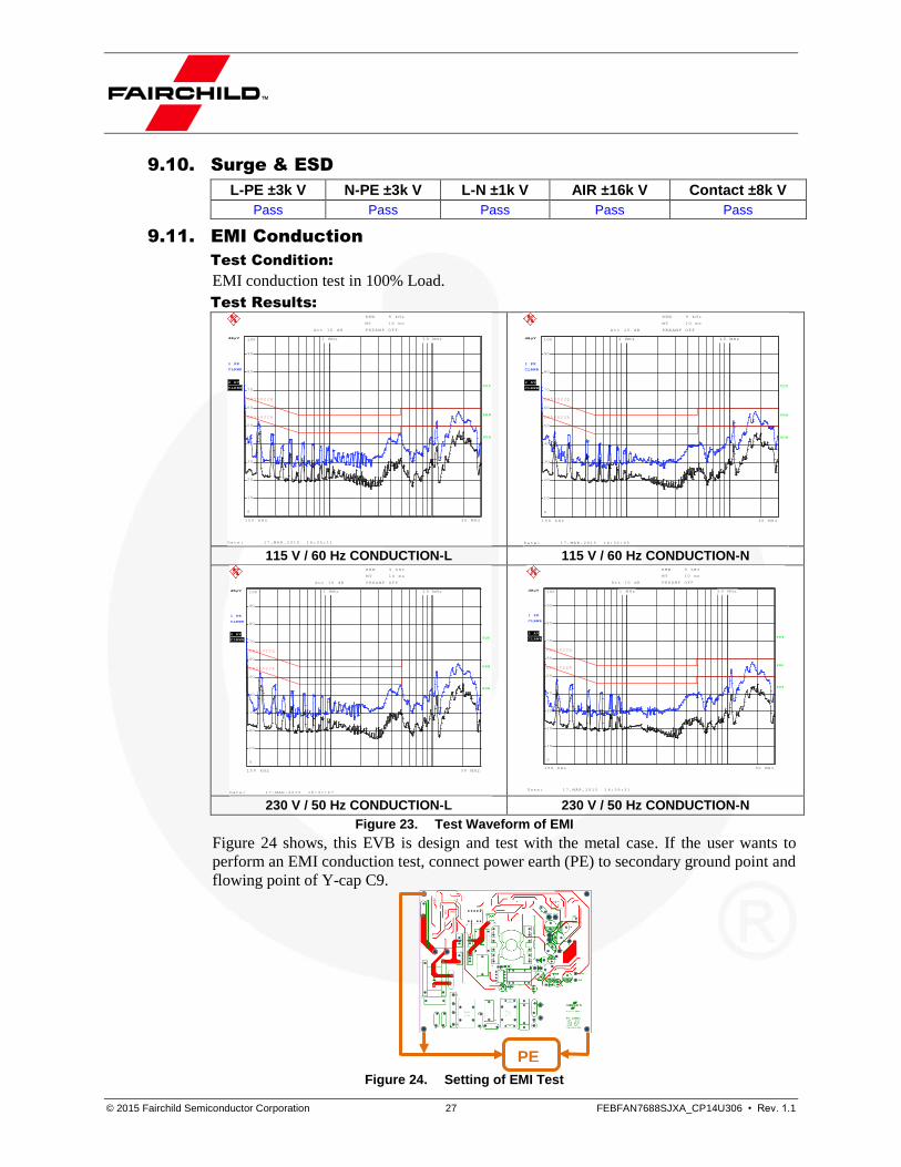
9.11. EMI Conduction
Test Condition:
EMI conduction test in 100% Load.
Test Results:
115 V / 60 Hz CONDUCTION-L 115 V / 60 Hz CONDUCTION-N
230 V / 50 Hz CONDUCTION-L 230 V / 50 Hz CONDUCTION-N
Figure 23. Test Waveform of EMI
Figure 24 shows, this EVB is design and test with the metal case. If the user wants to
perform an EMI conduction test, connect power earth (PE) to secondary ground point and
flowing point of Y-cap C9.
Figure 24. Setting of EMI Test
1 PK
CLRWR
2 AV
CLRWRTDF
6DB
dBµV
dBµV
150 kHz 30 MHz
MT 10 ms
RBW 9 kHz
PREAMP OFFAtt 10 dB
PRN
1 MHz 10 MHz
0
10
20
30
40
50
60
70
80
90
100
EN55022A
EN55022Q
Date: 17.MAR.2015 16:35:11
1 PK
CLRWR
2 AV
CLRWRTDF
6DB
dBµV
dBµV
150 kHz 30 MHz
MT 10 ms
RBW 9 kHz
PREAMP OFFAtt 10 dB
PRN
1 MHz 10 MHz
0
10
20
30
40
50
60
70
80
90
100
EN55022A
EN55022Q
Date: 17.MAR.2015 16:32:05
1 PK
CLRWR
2 AV
CLRWRTDF
6DB
dBµV
dBµV
150 kHz 30 MHz
MT 10 ms
RBW 9 kHz
PREAMP OFFAtt 10 dB
PRN
1 MHz 10 MHz
0
10
20
30
40
50
60
70
80
90
100
EN55022A
EN55022Q
Date: 17.MAR.2015 16:37:27
1 PK
CLRWR
2 AV
CLRWRTDF
6DB
dBµV
dBµV
150 kHz 30 MHz
MT 10 ms
RBW 9 kHz
PREAMP OFFAtt 10 dB
PRN
1 MHz 10 MHz
0
10
20
30
40
50
60
70
80
90
100
EN55022A
EN55022Q
Date: 17.MAR.2015 16:39:31
PE

© 2015 Fairchild Semiconductor Corporation 28 FEBFAN7688SJXA_CP14U306 • Rev. 1.1
10. Revision History
Rev. Date Description
1.0.0 May 2015 Initial release
1.1 September 2015 Correct Output power, page 4 306 kW to 306 W
WARNING AND DISCLAIMER
Replace components on the Evaluation Board only with those parts shown on the parts list (or Bill of Materials) in the Users’ Guide. Contact an authorized Fairchild representative with any questions.
This board is intended to be used by certified professionals, in a lab environment, following proper safety procedures. Use at your own risk. The Evaluation board (or kit) is for demonstration purposes only and neither the Board nor this User’s Guide constitute a sales contract or create any kind of warranty, whether express or implied, as to the applications or products involved. Fairchild warrantees that its products meet Fairchild’s published specifications, but does not guarantee that its products work in any specific application. Fairchild reserves the right to make changes without notice to any products described herein to improve reliability, function, or design. Either the applicable sales contract signed by Fairchild and Buyer or, if no contract exists, Fairchild’s standard Terms and Conditions on the back of Fairchild invoices, govern the terms of sale of the products described herein.
DISCLAIMER
FAIRCHILD SEMICONDUCTOR RESERVES THE RIGHT TO MAKE CHANGES WITHOUT FURTHER NOTICE TO ANY PRODUCTS HEREIN TO IMPROVE RELIABILITY, FUNCTION, OR DESIGN. FAIRCHILD DOES NOT ASSUME ANY LIABILITY ARISING OUT OF THE APPLICATION OR USE OF ANY PRODUCT OR CIRCUIT DESCRIBED HEREIN; NEITHER DOES IT CONVEY ANY LICENSE UNDER ITS PATENT RIGHTS, NOR THE RIGHTS OF OTHERS.
LIFE SUPPORT POLICY
FAIRCHILD’S PRODUCTS ARE NOT AUTHORIZED FOR USE AS CRITICAL COMPONENTS IN LIFE SUPPORT DEVICES OR SYSTEMS WITHOUT THE EXPRESS WRITTEN APPROVAL OF THE PRESIDENT OF FAIRCHILD SEMICONDUCTOR CORPORATION.
As used herein:
1. Life support devices or systems are devices or systems which, (a) are intended for surgical implant into the body, or (b) support or sustain life, or (c) whose failure to perform when properly used in accordance with instructions for use provided in the labeling, can be reasonably expected to result in significant injury to the user.
2. A critical component is any component of a life support device or system whose failure to perform can be reasonably expected to cause the failure of the life support device or system, or to affect its safety or effectiveness.
ANTI-COUNTERFEITING POLICY
Fairchild Semiconductor Corporation's Anti-Counterfeiting Policy. Fairchild's Anti-Counterfeiting Policy is also stated on our external website, www.fairchildsemi.com, under Sales Support.
Counterfeiting of semiconductor parts is a growing problem in the industry. All manufacturers of semiconductor products are experiencing counterfeiting of their parts. Customers who inadvertently purchase counterfeit parts experience many problems such as loss of brand reputation, substandard performance, failed applications, and increased cost of production and manufacturing delays. Fairchild is taking strong measures to protect ourselves and our customers from the proliferation of counterfeit parts. Fairchild strongly encourages customers to purchase Fairchild parts either directly from Fairchild or from Authorized Fairchild Distributors who are listed by country on our web page cited above. Products customers buy either from Fairchild directly or from Authorized Fairchild Distributors are genuine parts, have full traceability, meet Fairchild's quality standards for handling and storage and provide access to Fairchild's full range of up-to-date technical and product information. Fairchild and our Authorized Distributors will stand behind all warranties and will appropriately address any warranty issues that may arise. Fairchild will not provide any warranty coverage or other assistance for parts bought from Unauthorized Sources. Fairchild is committed to combat this global problem and encourage our customers to do their part in stopping this practice by buying direct or from authorized distributors.
EXPORT COMPLIANCE STATEMENT
These commodities, technology, or software were exported from the United States in accordance with the Export Administration Regulations for the ultimate destination listed on the commercial invoice. Diversion contrary to U.S. law is prohibited.
U.S. origin products and products made with U.S. origin technology are subject to U.S Re-export laws. In the event of re-export, the user will be responsible to ensure the appropriate U.S. export regulations are followed.