Embed Size (px)
Citation preview
100 N(1%)
6 x 100 N(optional)
2.9 V ± 5.5V
Control Signals
Auxiliary PowerPower SwitchStatus Signals
Type- C DFPStatus Signals
US
B T
ype-C
Co
nn
ector
VBUSIN1
IN2
EN
CHG
CHG_HI
REF
GND
OUT
FAULT
LD_DET
CC1
CC2
UFP
POL
AUDIO
DEBUG
Power Pad
TPS25810
AUX
CC Power 4.5 V ± 5.5V
120PF
6.8PFREF_RTN
4.5 V ± 6.5VBus Power
Copyright © 2016, Texas Instruments IncorporatedCopyright © 2016, Texas Instruments Incorporated
Product
Folder
Order
Now
Technical
Documents
Tools &
Software
Support &Community
An IMPORTANT NOTICE at the end of this data sheet addresses availability, warranty, changes, use in safety-critical applications,intellectual property matters and other important disclaimers. PRODUCTION DATA.
TPS25810SLVSCR1C –SEPTEMBER 2015–REVISED JULY 2017
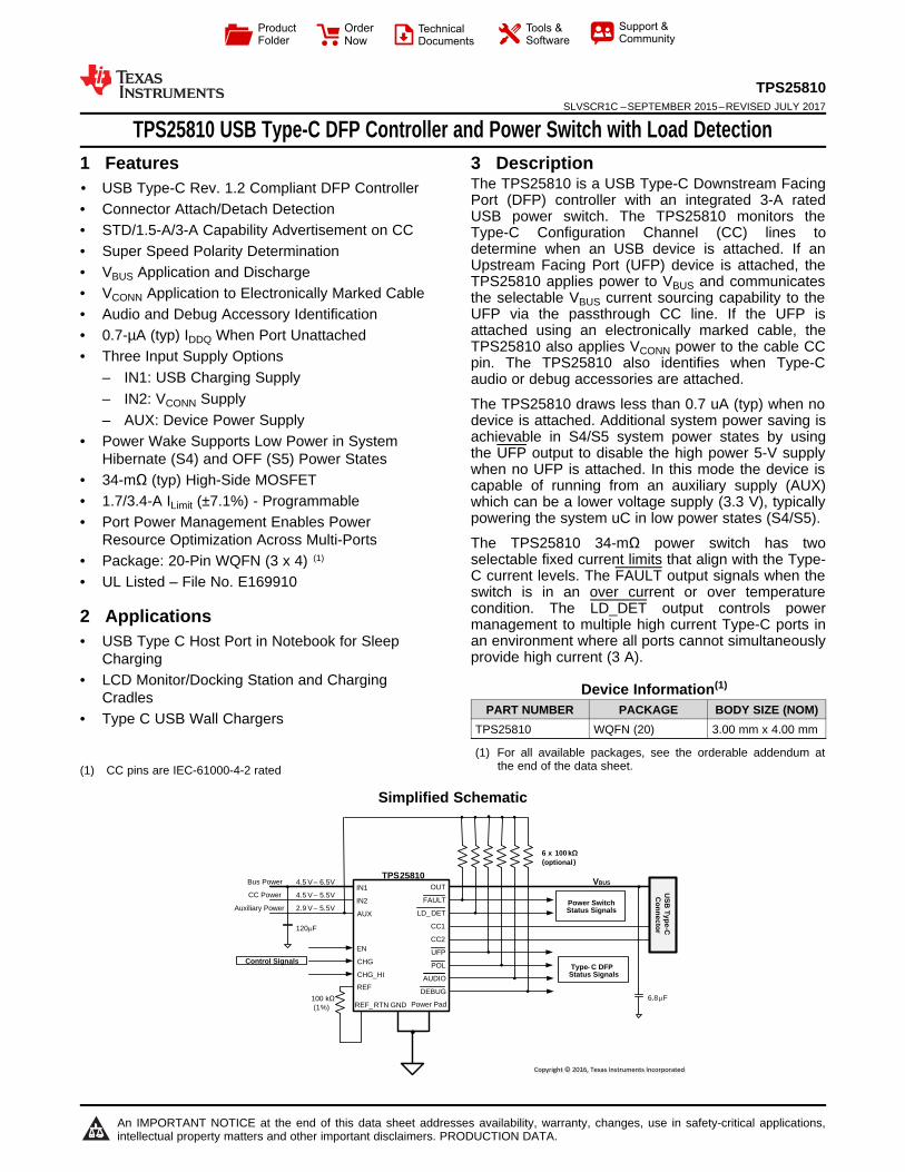
TPS25810 USB Type-C DFP Controller and Power Switch with Load Detection
1
(1) CC pins are IEC-61000-4-2 rated
1 Features1• USB Type-C Rev. 1.2 Compliant DFP Controller• Connector Attach/Detach Detection• STD/1.5-A/3-A Capability Advertisement on CC• Super Speed Polarity Determination• VBUS Application and Discharge• VCONN Application to Electronically Marked Cable• Audio and Debug Accessory Identification• 0.7-µA (typ) IDDQ When Port Unattached• Three Input Supply Options
– IN1: USB Charging Supply– IN2: VCONN Supply– AUX: Device Power Supply
• Power Wake Supports Low Power in SystemHibernate (S4) and OFF (S5) Power States
• 34-mΩ (typ) High-Side MOSFET• 1.7/3.4-A ILimit (±7.1%) - Programmable• Port Power Management Enables Power
Resource Optimization Across Multi-Ports• Package: 20-Pin WQFN (3 x 4) (1)
• UL Listed – File No. E169910
2 Applications• USB Type C Host Port in Notebook for Sleep
Charging• LCD Monitor/Docking Station and Charging
Cradles• Type C USB Wall Chargers
3 DescriptionThe TPS25810 is a USB Type-C Downstream FacingPort (DFP) controller with an integrated 3-A ratedUSB power switch. The TPS25810 monitors theType-C Configuration Channel (CC) lines todetermine when an USB device is attached. If anUpstream Facing Port (UFP) device is attached, theTPS25810 applies power to VBUS and communicatesthe selectable VBUS current sourcing capability to theUFP via the passthrough CC line. If the UFP isattached using an electronically marked cable, theTPS25810 also applies VCONN power to the cable CCpin. The TPS25810 also identifies when Type-Caudio or debug accessories are attached.
The TPS25810 draws less than 0.7 uA (typ) when nodevice is attached. Additional system power saving isachievable in S4/S5 system power states by usingthe UFP output to disable the high power 5-V supplywhen no UFP is attached. In this mode the device iscapable of running from an auxiliary supply (AUX)which can be a lower voltage supply (3.3 V), typicallypowering the system uC in low power states (S4/S5).
The TPS25810 34-mΩ power switch has twoselectable fixed current limits that align with the Type-C current levels. The FAULT output signals when theswitch is in an over current or over temperaturecondition. The LD_DET output controls powermanagement to multiple high current Type-C ports inan environment where all ports cannot simultaneouslyprovide high current (3 A).
Device Information(1)
PART NUMBER PACKAGE BODY SIZE (NOM)TPS25810 WQFN (20) 3.00 mm x 4.00 mm
(1) For all available packages, see the orderable addendum atthe end of the data sheet.
Simplified Schematic

2
TPS25810SLVSCR1C –SEPTEMBER 2015–REVISED JULY 2017 www.ti.com
Product Folder Links: TPS25810
Submit Documentation Feedback Copyright © 2015–2017, Texas Instruments Incorporated
Table of Contents1 Features .................................................................. 12 Applications ........................................................... 13 Description ............................................................. 14 Revision History..................................................... 25 Pin Configuration and Functions ......................... 36 Specifications......................................................... 4
6.1 Absolute Maximum Ratings ...................................... 46.2 ESD Ratings ............................................................ 46.3 Recommended Operating Conditions....................... 46.4 Thermal Information .................................................. 56.5 Electrical Characteristics........................................... 56.6 Switching Characteristics .......................................... 76.7 Typical Characteristics .............................................. 9
7 Detailed Description ............................................ 117.1 Overview ................................................................. 117.2 Functional Block Diagram ....................................... 137.3 Feature Description................................................. 13
7.4 Device Functional Modes........................................ 218 Application and Implementation ........................ 22
8.1 Application Information............................................ 228.2 Typical Applications ................................................ 22
9 Power Supply Recommendations ...................... 2710 Layout................................................................... 28
10.1 Layout Guidelines ................................................. 2810.2 Layout Example .................................................... 29
11 Device and Documentation Support ................. 3011.1 Device Support .................................................... 3011.2 Documentation Support ....................................... 3011.3 Receiving Notification of Documentation Updates 3011.4 Community Resources.......................................... 3011.5 Trademarks ........................................................... 3011.6 Electrostatic Discharge Caution............................ 3011.7 Glossary ................................................................ 30
12 Mechanical, Packaging, and OrderableInformation ........................................................... 30
4 Revision History
Changes from Revision B (May 2016) to Revision C Page
• Changed Feature From: USB Type-C Rev. 1.1 Compliant DFP Controller To: USB Type-C Rev. 1.2 Compliant DFPController ............................................................................................................................................................................... 1
• Changed text From: Type-C spec revision 1.1 To: Type-C spec revision 1.2 in the Overview section............................... 11• Replaced Figure 15 ............................................................................................................................................................. 18
Changes from Revision A (September 2015) to Revision B Page
• Added CC pins IEC-61000-4-2 rated footnote ....................................................................................................................... 1• Changed from UL and CB Tests Underway to UL Listed – File No. E169910 in Features ................................................... 1• Changed 10µF to 6.8µF in Simplified Schematic ................................................................................................................... 1• Added text to REF description ............................................................................................................................................... 3• Added IEC information to ESD Ratings ................................................................................................................................. 4• Changed IN2 II parameter description in Electrical Characteristics ...................................................................................... 7• Changed tres to tios in Switching Characteristics .................................................................................................................... 8• Added text to Detecting a Connection section .................................................................................................................... 12• Changed Rp to Rds in Figure 12 ......................................................................................................................................... 12• Changed loss to drop in Figure 14 ...................................................................................................................................... 16• Added text and Figure 15 to Plug Polarity Detection ........................................................................................................... 18• Added last sentence to Input and Output Capacitance ....................................................................................................... 23• Added ESD Considerations to Layout Guidelines................................................................................................................ 28• Added Protecting the TPS25810 from High Voltage DFPs to Related Documentation ....................................................... 30
Changes from Original (September 2015) to Revision A Page
• Changed from Product Preview to Production Data............................................................................................................... 1
Thermal Pad
7
2
3
6
8 9 10
11
12
13
14
20
1
19 18 17
15
16
4
5
FAULT
IN1
IN1
IN2
AUX
ENC
HG
CH
G_
HI
RE
F
CC1
CC2
GND
OUT
OUT
DEBUG
AU
DIO
PO
L
UF
P
LD_
DE
T
RE
F_
RT
N
3
TPS25810www.ti.com SLVSCR1C –SEPTEMBER 2015–REVISED JULY 2017
Product Folder Links: TPS25810
Submit Documentation FeedbackCopyright © 2015–2017, Texas Instruments Incorporated
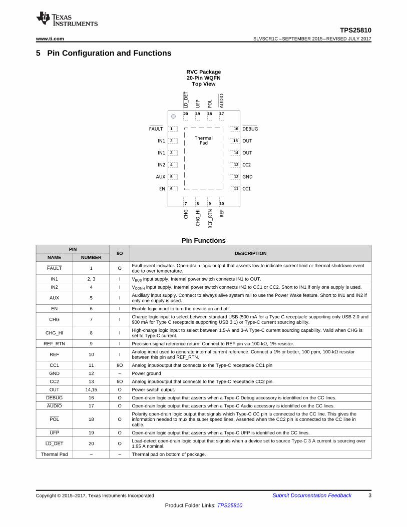
5 Pin Configuration and Functions
RVC Package20-Pin WQFN
Top View
Pin FunctionsPIN
I/O DESCRIPTIONNAME NUMBER
FAULT 1 O Fault event indicator. Open-drain logic output that asserts low to indicate current limit or thermal shutdown eventdue to over temperature.
IN1 2, 3 I VBUS input supply. Internal power switch connects IN1 to OUT.
IN2 4 I VCONN input supply. Internal power switch connects IN2 to CC1 or CC2. Short to IN1 if only one supply is used.
AUX 5 I Auxiliary input supply. Connect to always alive system rail to use the Power Wake feature. Short to IN1 and IN2 ifonly one supply is used.
EN 6 I Enable logic input to turn the device on and off.
CHG 7 I Charge logic input to select between standard USB (500 mA for a Type C receptacle supporting only USB 2.0 and900 mA for Type C receptacle supporting USB 3.1) or Type-C current sourcing ability.
CHG_HI 8 I High-charge logic input to select between 1.5-A and 3-A Type-C current sourcing capability. Valid when CHG isset to Type-C current.
REF_RTN 9 I Precision signal reference return. Connect to REF pin via 100-kΩ, 1% resistor.
REF 10 I Analog input used to generate internal current reference. Connect a 1% or better, 100 ppm, 100-kΩ resistorbetween this pin and REF_RTN.
CC1 11 I/O Analog input/output that connects to the Type-C receptacle CC1 pin
GND 12 – Power ground
CC2 13 I/O Analog input/output that connects to the Type-C receptacle CC2 pin.
OUT 14,15 O Power switch output.
DEBUG 16 O Open-drain logic output that asserts when a Type-C Debug accessory is identified on the CC lines.
AUDIO 17 O Open-drain logic output that asserts when a Type-C Audio accessory is identified on the CC lines.
POL 18 OPolarity open-drain logic output that signals which Type-C CC pin is connected to the CC line. This gives theinformation needed to mux the super speed lines. Asserted when the CC2 pin is connected to the CC line incable.
UFP 19 O Open-drain logic output that asserts when a Type-C UFP is identified on the CC lines.
LD_DET 20 O Load-detect open-drain logic output that signals when a device set to source Type-C 3 A current is sourcing over1.95 A nominal.
Thermal Pad – – Thermal pad on bottom of package.

4
TPS25810SLVSCR1C –SEPTEMBER 2015–REVISED JULY 2017 www.ti.com
Product Folder Links: TPS25810
Submit Documentation Feedback Copyright © 2015–2017, Texas Instruments Incorporated
(1) Stresses beyond those listed under Absolute Maximum Ratings may cause permanent damage to the device. These are stress ratingsonly, which do not imply functional operation of the device at these or any other conditions beyond those indicated under RecommendedOperating Conditions. Exposure to absolute-maximum-rated conditions for extended periods may affect device reliability.
6 Specifications
6.1 Absolute Maximum Ratingsover operating free-air temperature range, voltages are respect to GND (unless otherwise noted) (1)
MIN MAX UNIT
Pin voltage, V
IN1, IN2, AUX, EN, CHG, CHG_HI, REF, OUT, LD_DET,FAULT, CC1, CC2, UFP, POL, AUDIO, DEBUG –0.3 7 V
REF_RTNInternallyconnected
to GNDV
Pin positive source current, ISRC OUT, REF, CC1, CC2 Internallylimited A
Pin positive sink current, ISNK
OUT (while applying VBUS) 5 ACC1, CC2 (while applying VCONN) 1 A
LD_DET, FAULT, UFP, POL, AUDIO, DEBUG Internallylimited mA
Operating junction temperature, TJ –40 180 °CStorage temperature range, Tstg –65 150 °C
(1) Electrostatic discharge (ESD) to measure device sensitivity/immunity to damage caused by assembly line electrostatic discharges intothe device.
(2) JEDEC document JEP155 states that 500-V HBM allows safe manufacturing with a standard ESD control process.(3) JEDEC document JEP157 states that 250-V CDM allows safe manufacturing with a standard ESD control process.(4) Surges per IEC61000-402, 1999 applied between CC1/CC2 and output ground of the TPS25810EVM-745.
6.2 ESD RatingsVALUE UNIT
V(ESD)(1) Electrostatic
discharge
Human-body model (HBM), per ANSI/ESDA/JEDEC JS-001 (2) ±2000
VCharged-device model (CDM), per JEDEC specification JESD22-C101 (3) ±500
IEC (4) IEC61000-4-2 contact discharge, CC1 and CC2 ±8000IEC61000-4-2 air discharge, CC1 and CC2 ±15000
6.3 Recommended Operating ConditionsVoltages are with respect to GND (unless otherwise noted)
MIN NOM MAX UNIT
VI Supply voltageIN1 4.5 6.5
VIN2 4.5 5.5AUX 2.9 5.5
VI Input voltage EN, CHG, CHG_HI 0 5.5 VVIH High-level input voltage EN, CHG, CHG_HI 1.17 VVIL Low-level voltage EN, CHG, CHG_HI 0.63 V
VPU Pull-up voltage Used on LD_DET, FAULT, UFP, POL, AUDIO,DEBUG 0 5.5 V
ISRC Positive source currentOUT 3 ACC1 or CC2 when supplying VCONN 250 mA
ISNKPositive sink current (10 ms movingaverage) LD_DET, FAULT, UFP, POL, AUDIO, DEBUG 10 mA
ISNK_PULSE Positive repetitive pulse sink current LD_DET, FAULT, UFP, POL, AUDIO, DEBUG InternallyLimited mA
RREF Reference Resistor 98 100 102 kΩTJ Operating junction temperature –40 125 °C
5
TPS25810www.ti.com SLVSCR1C –SEPTEMBER 2015–REVISED JULY 2017
Product Folder Links: TPS25810
Submit Documentation FeedbackCopyright © 2015–2017, Texas Instruments Incorporated
(1) For more information about traditional and new thermal metrics, see the Semiconductor and IC Package Thermal Metrics applicationreport.
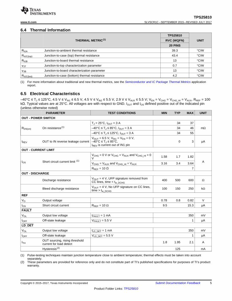
6.4 Thermal Information
THERMAL METRIC (1)TPS25810
UNITRVC (WQFN)20 PINS
RθJA Junction-to-ambient thermal resistance 39.3 °C/WRθJC(top) Junction-to-case (top) thermal resistance 43.4 °C/WRθJB Junction-to-board thermal resistance 13 °C/WψJT Junction-to-top characterization parameter 0.7 °C/WψJB Junction-to-board characterization parameter 13 °C/WRθJC(bot) Junction-to-case (bottom) thermal resistance 4.2 °C/W
(1) Pulse-testing techniques maintain junction temperature close to ambient temperature; thermal effects must be taken into accountseparately.
(2) These parameters are provided for reference only and do not constitute part of TI’s published specifications for purposes of TI’s productwarranty.
6.5 Electrical Characteristics–40°C ≤ TJ ≤ 125°C, 4.5 V ≤ VIN1 ≤ 6.5 V, 4.5 V ≤ VIN2 ≤ 5.5 V, 2.9 V ≤ VAUX ≤ 5.5 V; VEN = VCHG = VCHG_HI = VAUX, RREF = 100kΩ. Typical values are at 25°C. All voltages are with respect to GND. IOUT and IOS defined positive out of the indicated pin(unless otherwise noted)
PARAMETER TEST CONDITIONS MIN TYP MAX UNITOUT - POWER SWITCH
RDS(on) On resistance (1)
TJ = 25°C, IOUT = 3 A 34 37mΩ–40°C ≤ TJ ≤ 85°C, IOUT = 3 A 34 46
–40°C ≤ TJ ≤ 125°C, IOUT = 3 A 34 55
IREV OUT to IN reverse leakage currentVOUT = 6.5 V, VIN1 = VEN = 0 V,–40°C ≤ TJ ≤ 85°C,IREV is current out of IN1 pin
0 3 µA
OUT - CURRENT LIMIT
IOS Short circuit current limit (1)
VCHG = 0 V or VCHG = VAUX and VCHG_HI = 0V 1.58 1.7 1.82
AVCHG = VAUX and VCHG_HI = VAUX 3.16 3.4 3.64RREF = 10 Ω 7
OUT - DISCHARGE
Discharge resistance VOUT = 4 V, UFP signature removed fromCC lines, time < tw_DCHG
400 500 600 Ω
Bleed discharge resistance VOUT = 4 V, No UFP signature on CC lines,time > tw_DCHG
100 150 250 kΩ
REFVO Output voltage 0.78 0.8 0.82 VIOS Short circuit current RREF = 10 Ω 9.5 15.3 µAFAULTVOL Output low voltage IFAULT = 1 mA 350 mVIOFF Off-state leakage VFAULT = 5.5 V 1 µALD_DETVOL Output low voltage ILD_DET = 1 mA 350 mVIOFF Off-state leakage VLD_DET = 5.5 V 1 µA
ITHOUT sourcing, rising thresholdcurrent for load detect 1.8 1.95 2.1 A
Hysteresis (2) 125 mA

6
TPS25810SLVSCR1C –SEPTEMBER 2015–REVISED JULY 2017 www.ti.com
Product Folder Links: TPS25810
Submit Documentation Feedback Copyright © 2015–2017, Texas Instruments Incorporated
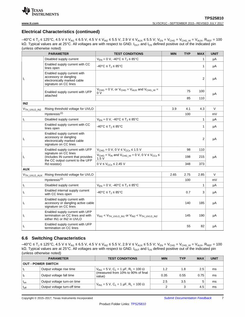
Electrical Characteristics (continued)–40°C ≤ TJ ≤ 125°C, 4.5 V ≤ VIN1 ≤ 6.5 V, 4.5 V ≤ VIN2 ≤ 5.5 V, 2.9 V ≤ VAUX ≤ 5.5 V; VEN = VCHG = VCHG_HI = VAUX, RREF = 100kΩ. Typical values are at 25°C. All voltages are with respect to GND. IOUT and IOS defined positive out of the indicated pin(unless otherwise noted)
PARAMETER TEST CONDITIONS MIN TYP MAX UNITCC1/CC2 - VCONN POWER SWITCH
RDS(on) On resistanceTJ = 25°C, IOUT = 250 mA 365 420
mΩ-40°C ≤ TJ ≤ 85°C, IOUT = 250 mA 365 530-40°C ≤ TJ ≤ 125°C, IOUT = 250 mA 365 600
CC1/CC2 - VCONN POWER SWITCH - CURRENT LIMIT
IOS Short circuit current limit (1) 300 355 410mA
RREF = 10 Ω 800CC1/CC2 – CONNECT MANAGEMENT – DANGLING ELECTRONICALLY MARKED CABLE MODE
ISRC
Sourcing current on the pass-through CC Line 0 V ≤ VCCx ≤ 1.5 V 64 80 96 µA
Sourcing current on the Ra CCline 0 V ≤ VCCx ≤ 1.5 V 64 80 96 µA
CC1/CC2 – CONNECT MANAGEMENT – ACCESSORY MODE
ISRC
CCx Sourcing current(CC2- Audio, CC1-Debug) 0 V ≤ VCCx ≤ 1.5 V 64 80 96 µA
CCx Sourcing current(CC1- Audio, CC2-Debug) (2) 0 V ≤ VCCx ≤ 1.5 V 0 µA
CC1/CC2 – CONNECT MANAGEMENT – UFP MODE
ISRCSourcing current with either IN1 orIN2 in UVLO
0 V ≤ VCCx ≤ 1.5 VVIN1 < VTH_UVLO_IN1 or VIN2 < VTH_UVLO_IN2
64 80 96 µA
ISRC Sourcing current
VCHG = 0 V and VCHG_HI = 0 V0 V ≤ VCCx ≤ 1.5 V 75 80 85
µAVCHG = VAUX and VCHG_HI = 0 V0 V ≤ VCCx ≤ 1.5 V 170 180 190
VCHG = VAUX and VCHG_HI = VAUX0 V ≤ VCCx ≤ 2.45 V 312 330 348
UFP, POL, AUDIO, DEBUGVOL Output low voltage ISNK_PIN = 1 mA 250 mVIOFF Off-state leakage VPIN = 5.5 V 1 µAEN, CHG, CHG_HI - LOGIC INPUTSVTH Rising threshold voltage 0.925 1.15 VVTH Falling threshold voltage 0.65 0.875 V
Hysteresis (2) 50 mVIIN Input current VEN = 0 V or 6.5 V –0.5 0.5 µAOVER TEMPERATURE SHUT DOWN
TTH_OTSD2Rising threshold temperature fordevice shutdown 155 °C
Hysteresis (2) 20 °C
TTH_OTSD1
Rising threshold temperature forOUT/ VCONN switch shutdown incurrent limit
135 °C
Hysteresis (2) 20 °CIN1VTH_UVLO_IN1 Rising threshold voltage for UVLO 3.9 4.1 4.3 V
Hysteresis (2) 100 mV
7
TPS25810www.ti.com SLVSCR1C –SEPTEMBER 2015–REVISED JULY 2017
Product Folder Links: TPS25810
Submit Documentation FeedbackCopyright © 2015–2017, Texas Instruments Incorporated
Electrical Characteristics (continued)–40°C ≤ TJ ≤ 125°C, 4.5 V ≤ VIN1 ≤ 6.5 V, 4.5 V ≤ VIN2 ≤ 5.5 V, 2.9 V ≤ VAUX ≤ 5.5 V; VEN = VCHG = VCHG_HI = VAUX, RREF = 100kΩ. Typical values are at 25°C. All voltages are with respect to GND. IOUT and IOS defined positive out of the indicated pin(unless otherwise noted)
PARAMETER TEST CONDITIONS MIN TYP MAX UNIT
II
Disabled supply current VEN = 0 V, -40°C ≤ TJ ≤ 85°C 1 µAEnabled supply current with CClines open -40°C ≤ TJ ≤ 85°C 1 µA
Enabled supply current withaccessory or danglingelectronically marked cablesignature on CC lines
2 µA
Enabled supply current with UFPattached
VCHG = 0 V, or VCHG = VAUX and VCHG_HI =0 V 75 100
µA85 110
IN2VTH_UVLO_IN2 Rising threshold voltage for UVLO 3.9 4.1 4.3 V
Hysteresis (2) 100 mVII Disabled supply current VEN = 0 V, -40°C ≤ TJ ≤ 85°C 1 µA
Enabled supply current with CClines open -40°C ≤ TJ ≤ 85°C 1 µA
II
Enabled supply current withaccessory or danglingelectronically marked cablesignature on CC lines
2 µA
II
Enabled supply current with UFPsignature on CC lines(Includes IN current that providesthe CC output current to the UFPRd resistor)
VCHG = 0 V, 0 V ≤ VCCx ≤ 1.5 V 98 110
µAVCHG = VIN and VCHG_HI = 0 V, 0 V ≤ VCCx ≤1.5 V 198 215
0 V ≤ VCCx ≤ 2.45 V 348 373
AUXVTH_UVLO_AUX Rising threshold voltage for UVLO 2.65 2.75 2.85 V
Hysteresis (2) 100 mVII Disabled supply current VEN = 0 V, -40°C ≤ TJ ≤ 85°C 1 µA
IIEnabled internal supply currentwith CC lines open -40°C ≤ TJ ≤ 85°C 0.7 3 µA
IIEnabled supply current withaccessory or dangling active cablesignature on CC lines
140 185 µA
IIEnabled supply current with UFPtermination on CC lines and witheither IN1 or IN2 in UVLO
VIN1 < VTH_UVLO_IN1 or VIN2 < VTH_UVLO_IN2 145 190 µA
IIEnabled supply current with UFPtermination on CC lines 55 82 µA
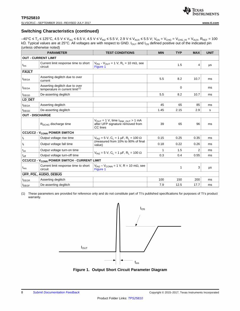
6.6 Switching Characteristics–40°C ≤ TJ ≤ 125°C, 4.5 V ≤ VIN1 ≤ 6.5 V, 4.5 V ≤ VIN2 ≤ 5.5 V, 2.9 V ≤ VAUX ≤ 5.5 V; VEN = VCHG = VCHG_HI = VAUX, RREF = 100kΩ. Typical values are at 25°C. All voltages are with respect to GND. IOUT and IOS defined positive out of the indicated pin(unless otherwise noted)
PARAMETER TEST CONDITIONS MIN TYP MAX UNITOUT - POWER SWITCHtr Output voltage rise time VIN1 = 5 V, CL = 1 µF, RL = 100 Ω
(measured from 10% to 90% of finalvalue)
1.2 1.8 2.5 ms
tf Output voltage fall time 0.35 0.55 0.75 ms
ton Output voltage turn-on timeVIN1 = 5 V, CL = 1 µF, RL = 100 Ω
2.5 3.5 5 mstoff Output voltage turn-off time 2 3 4.5 ms
tios
IOS
IOUT
8
TPS25810SLVSCR1C –SEPTEMBER 2015–REVISED JULY 2017 www.ti.com
Product Folder Links: TPS25810
Submit Documentation Feedback Copyright © 2015–2017, Texas Instruments Incorporated
Switching Characteristics (continued)–40°C ≤ TJ ≤ 125°C, 4.5 V ≤ VIN1 ≤ 6.5 V, 4.5 V ≤ VIN2 ≤ 5.5 V, 2.9 V ≤ VAUX ≤ 5.5 V; VEN = VCHG = VCHG_HI = VAUX, RREF = 100kΩ. Typical values are at 25°C. All voltages are with respect to GND. IOUT and IOS defined positive out of the indicated pin(unless otherwise noted)
PARAMETER TEST CONDITIONS MIN TYP MAX UNIT
(1) These parameters are provided for reference only and do not constitute part of TI’s published specifications for purposes of TI’s productwarranty.
OUT - CURRENT LIMIT
tiosCurrent limit response time to shortcircuit
VIN1 - VOUT = 1 V, RL = 10 mΩ, seeFigure 1 1.5 4 µs
FAULT
tDEGAAsserting deglitch due to overcurrent 5.5 8.2 10.7 ms
tDEGAAsserting deglitch due to overtemperature in current limit (1) 0 ms
tDEGD De-asserting deglitch 5.5 8.2 10.7 msLD_DETtDEGA Asserting deglitch 45 65 85 mstDEGD De-asserting deglitch 1.45 2.15 2.9 sOUT - DISCHARGE
RDCHG discharge timeVOUT = 1 V, time ISNK_OUT > 1 mAafter UFP signature removed fromCC lines
39 65 96 ms
CC1/CC2 - VCONN POWER SWITCHtr Output voltage rise time VIN2 = 5 V, CL = 1 µF, RL = 100 Ω
(measured from 10% to 90% of finalvalue)
0.15 0.25 0.35 ms
tf Output voltage fall time 0.18 0.22 0.26 ms
ton Output voltage turn-on timeVIN2 = 5 V, CL = 1 µF, RL = 100 Ω
1 1.5 2 mstoff Output voltage turn-off time 0.3 0.4 0.55 msCC1/CC2 - VCONN POWER SWITCH - CURRENT LIMIT
tresCurrent limit response time to shortcircuit
VIN2 – VCONN = 1 V, R = 10 mΩ, seeFigure 1 1 3 µs
UFP, POL, AUDIO, DEBUGtDEGR Asserting deglitch 100 150 200 mstDEGF De-asserting deglitch 7.9 12.5 17.7 ms
Figure 1. Output Short Circuit Parameter Diagram
TJ - Junction Temperature (oC)
LD_D
ET
Thr
esho
ld (
mA
)
-40 -25 -10 5 20 35 50 65 80 95 110 1251750
1770
1790
1810
1830
1850
1870
1890
1910
1930
1950
1970
1990
2010
D001
LD_DET Threshold RisingLD_DET Threshold Falling
TJ - Junction Temperature (oC)
Sou
rcin
g C
urre
nt (P
A)
-40 -25 -10 5 20 35 50 65 80 95 110 12550
100
150
200
250
300
350
D001
UFP 3 AUFP 1.5 AUFP 0.5 A/0.9 A
TJ - Junction Temperature (oC)
I RE
V -
Rev
erse
Lea
kage
Cur
rent
(µ
A)
-40 -25 -10 5 20 35 50 65 80 95 110 1250
0.05
0.1
0.15
0.2
0.25
D001TJ - Junction Temperature (oC)
I LIM
- L
imit
Cur
rent
(m
A)
-40 -25 -10 5 20 35 50 65 80 95 110 1250
500
1000
1500
2000
2500
3000
3500
4000
D001
VBUS ILIM 3 AVBUS ILIM 1.5 AVCONN_ILIM
TJ - Junction Temperature (oC)
RD
S(O
N) -
On
Res
ista
nce
(m:
)
-40 -25 -10 5 20 35 50 65 80 95 110 1250
10
20
30
40
50
D001TJ - Junction Temperature (oC)
RD
S(O
N) -
On
Res
ista
nce
(m:
)
-40 -25 -10 5 20 35 50 65 80 95 110 125250
300
350
400
450
500
D001
9
TPS25810www.ti.com SLVSCR1C –SEPTEMBER 2015–REVISED JULY 2017
Product Folder Links: TPS25810
Submit Documentation FeedbackCopyright © 2015–2017, Texas Instruments Incorporated
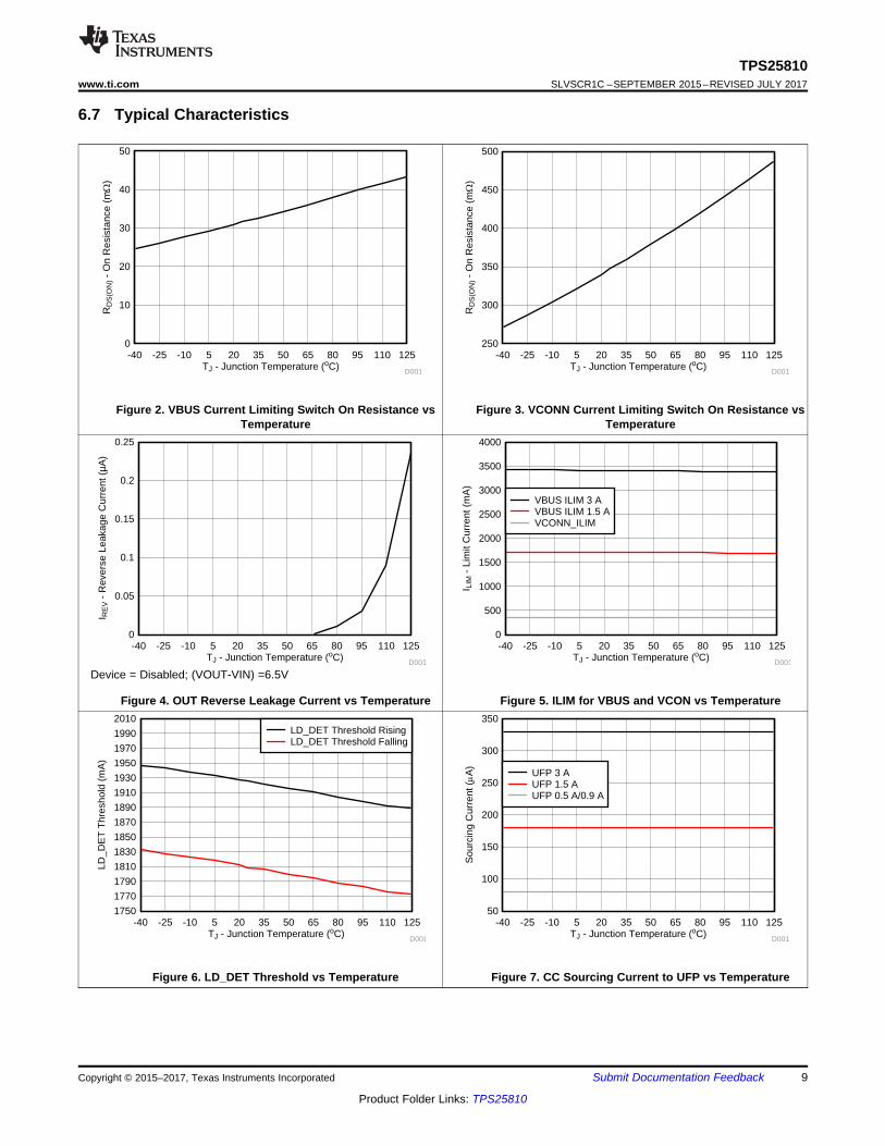
6.7 Typical Characteristics
Figure 2. VBUS Current Limiting Switch On Resistance vsTemperature
Figure 3. VCONN Current Limiting Switch On Resistance vsTemperature
Device = Disabled; (VOUT-VIN) =6.5V
Figure 4. OUT Reverse Leakage Current vs Temperature Figure 5. ILIM for VBUS and VCON vs Temperature
Figure 6. LD_DET Threshold vs Temperature Figure 7. CC Sourcing Current to UFP vs Temperature

TJ - Junction Temperature (oC)
I IN_O
N -
Ena
bled
IN S
uppl
y C
urre
nt (
µA
)
-40 -25 -10 5 20 35 50 65 80 95 110 12540
45
50
55
60
65
70
D001
TJ - Junction Temperature (oC)
I IN_O
N -
Ena
bled
IN S
uppl
y C
urre
nt (P
A)
-40 -25 -10 5 20 35 50 65 80 95 110 12570
75
80
85
90
95
100
D001
IN1 UFP 3 AIN1 UFP 0.5 A/1.5 A
TJ - Junction Temperature (oC)
I IN_O
N -
Ena
bled
IN S
uppl
y C
urre
nt (P
A)
-40 -25 -10 5 20 35 50 65 80 95 110 12550
100
150
200
250
300
350
400
D001
IN2 UFP 3 AIN2 UFP 1.5 AIN2 UFP 0.5 A
10
TPS25810SLVSCR1C –SEPTEMBER 2015–REVISED JULY 2017 www.ti.com
Product Folder Links: TPS25810
Submit Documentation Feedback Copyright © 2015–2017, Texas Instruments Incorporated
Typical Characteristics (continued)
Figure 8. IN1 Current with UFP vs Temperature Figure 9. IN2 Current with UFP vs Temperature
VAUX = 5 V
Figure 10. AUX Current with UFP vs Temperature
11
TPS25810www.ti.com SLVSCR1C –SEPTEMBER 2015–REVISED JULY 2017
Product Folder Links: TPS25810
Submit Documentation FeedbackCopyright © 2015–2017, Texas Instruments Incorporated
(1) This may be automatic or manually driven.
7 Detailed Description
7.1 OverviewThe TPS25810 is a highly integrated USB Type-C Downstream Facing Port (DFP) controller with built-in powerswitch developed for the new USB Type-C connector and cable. The part provides all functionality needed tosupport a USB Type C DFP in a system where USB power delivery (PD) source capabilities (for example, VBUS> 5 V) are not implemented. The device is designed to be compliant to Type-C spec revision 1.2.
7.1.1 USB Type C BasicFor a detailed description of the Type-C spec refer to the USB-IF website to download the latest releasedversion. Some of the basic concepts of the Type-C spec that pertains to understanding the operation of theTPS25810 (a DFP device) are described as follows.
USB Type-C removes the need for different plug and receptacle types for host and device functionality. TheType-C receptacle replaces both Type-A and Type-B receptacle since the Type-C cable is plug-able in eitherdirection between host and device. A host-to-device logical relationship is maintained via the configurationchannel (CC). Optionally hosts and devices can be either providers or consumers of power when USB PDcommunication is used to swap roles.
All USB Type-C ports operate in one of below three data modes:• Host mode: the port can only be host (provider of power)• Device mode: the port can only be device (consumer of power)• Dual-Role mode: the port can be either host or device
Port types:• DFP (Downstream Facing Port): Host• UFP (Upstream Facing Port): Device• DRP (Dual-Role Port): Host or Device
Valid DFP-to-UFP connections:• Table 1 describes valid DFP-to-UFP connections• Host to Host or Device to Device have no functions
Table 1. DFP-to-UFP Connections
HOST-MODE PORT DEVICE-MODEPORT DUAL-ROLE PORT
Host-Mode Port No Function Works WorksDevice-Mode Port Works No Function Works
Dual-Role Port Works Works Works (1)
7.1.2 Configuration ChannelThe function of the configuration channel is to detect connections and configure the interface across the USBType-C cables and connectors.
Functionally the Configuration Channel (CC) is used to serve the following purposes:• Detect connect to the USB ports• Resolve cable orientation and twist connections to establish USB data bus routing• Establish DFP and UFP roles between two connected ports• Discover and configure power: USB Type-C current modes or USB Power Delivery• Discovery and configure optional Alternate and Accessory modes• Enhances flexibility and ease of use
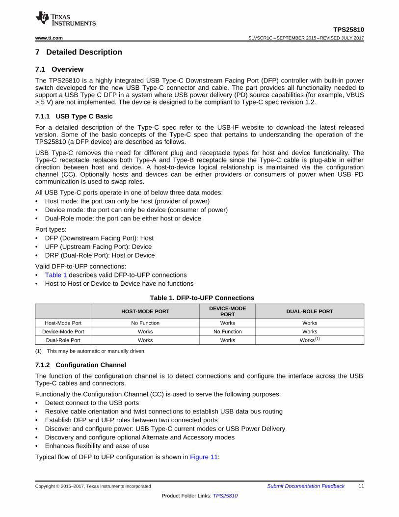
Typical flow of DFP to UFP configuration is shown in Figure 11:
Rp
Rp
CCRds
RdsRaRa
Cable
DFP monitors for connection
DFP monitors for connection
UFP monitors for connection
UFP monitors for connection
12
TPS25810SLVSCR1C –SEPTEMBER 2015–REVISED JULY 2017 www.ti.com
Product Folder Links: TPS25810
Submit Documentation Feedback Copyright © 2015–2017, Texas Instruments Incorporated
Figure 11. Flow of DFP to UFP Configuration
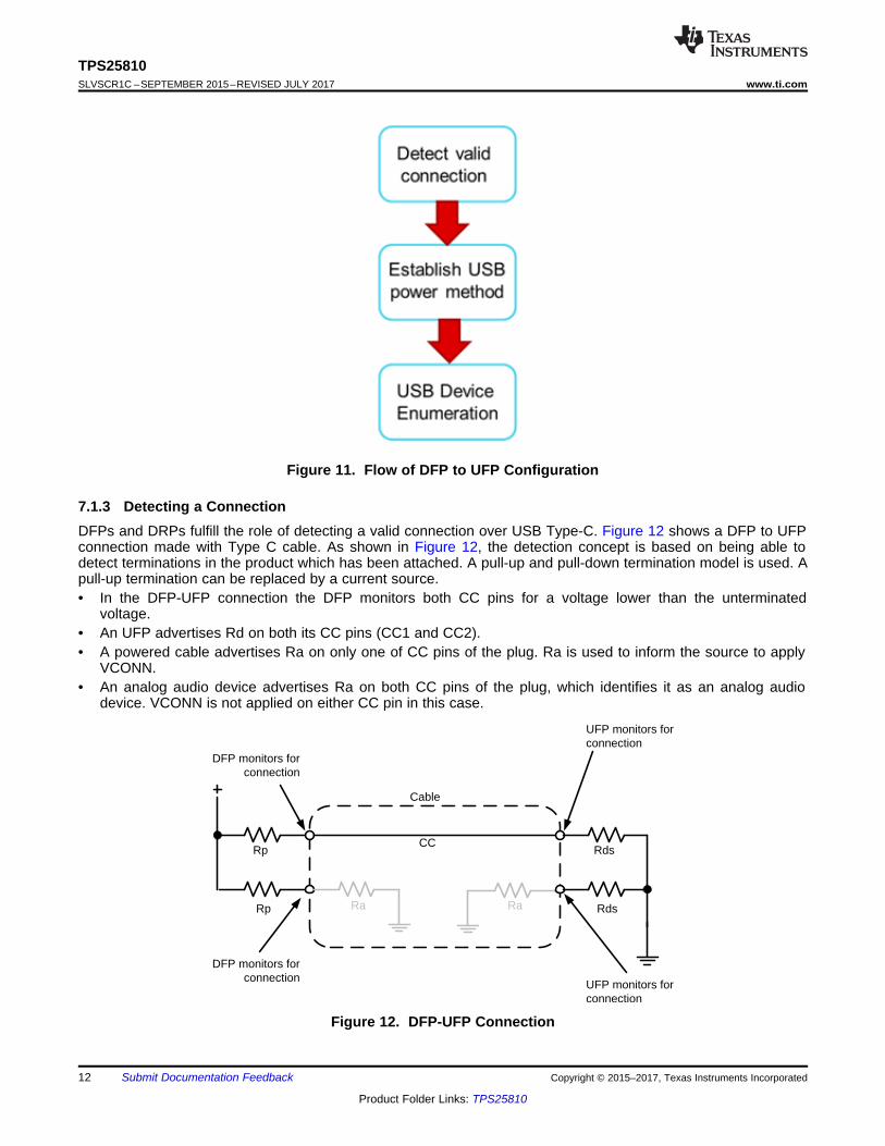
7.1.3 Detecting a ConnectionDFPs and DRPs fulfill the role of detecting a valid connection over USB Type-C. Figure 12 shows a DFP to UFPconnection made with Type C cable. As shown in Figure 12, the detection concept is based on being able todetect terminations in the product which has been attached. A pull-up and pull-down termination model is used. Apull-up termination can be replaced by a current source.• In the DFP-UFP connection the DFP monitors both CC pins for a voltage lower than the unterminated
voltage.• An UFP advertises Rd on both its CC pins (CC1 and CC2).• A powered cable advertises Ra on only one of CC pins of the plug. Ra is used to inform the source to apply
VCONN.• An analog audio device advertises Ra on both CC pins of the plug, which identifies it as an analog audio
device. VCONN is not applied on either CC pin in this case.
Figure 12. DFP-UFP Connection
Charge
PumpCurrent
Limit
OTSD
Thermal
Sense
IN1 Current Sense
IN2 Current Sense
Current Sense
AUX
EN
OUT
CC1
CC2
Gate
Control
LD_DET
FAULT
UFP
POL
AUDIO
DEBUG
Control
Logic
CC
Monitor
CHG
CHG_HI
REF_RTN
REF
UVLO
UVLO
UVLO
Copyright © 2016, Texas Instruments Incorporated
13
TPS25810www.ti.com SLVSCR1C –SEPTEMBER 2015–REVISED JULY 2017
Product Folder Links: TPS25810
Submit Documentation FeedbackCopyright © 2015–2017, Texas Instruments Incorporated
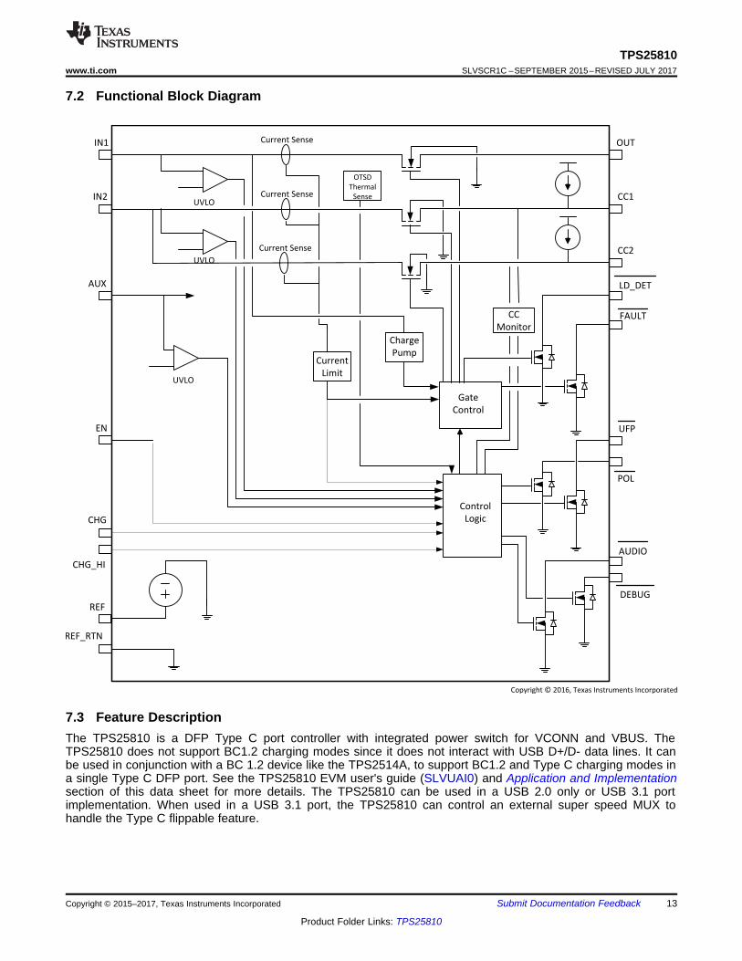
7.2 Functional Block Diagram
7.3 Feature DescriptionThe TPS25810 is a DFP Type C port controller with integrated power switch for VCONN and VBUS. TheTPS25810 does not support BC1.2 charging modes since it does not interact with USB D+/D- data lines. It canbe used in conjunction with a BC 1.2 device like the TPS2514A, to support BC1.2 and Type C charging modes ina single Type C DFP port. See the TPS25810 EVM user's guide (SLVUAI0) and Application and Implementationsection of this data sheet for more details. The TPS25810 can be used in a USB 2.0 only or USB 3.1 portimplementation. When used in a USB 3.1 port, the TPS25810 can control an external super speed MUX tohandle the Type C flippable feature.
14
TPS25810SLVSCR1C –SEPTEMBER 2015–REVISED JULY 2017 www.ti.com
Product Folder Links: TPS25810
Submit Documentation Feedback Copyright © 2015–2017, Texas Instruments Incorporated
Feature Description (continued)
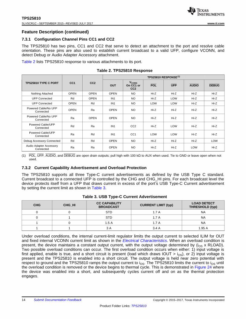
(1) POL, UFP, AUDIO, and DEBUG are open drain outputs; pull high with 100 kΩ to AUX when used. Tie to GND or leave open when notused.
7.3.1 Configuration Channel Pins CC1 and CC2The TPS25810 has two pins, CC1 and CC2 that serve to detect an attachment to the port and resolve cableorientation. These pins are also used to establish current broadcast to a valid UFP, configure VCONN, anddetect Debug or Audio Adapter Accessory attachment.
Table 2 lists TPS25810 response to various attachments to its port.
Table 2. TPS25810 Response
TPS25810 TYPE C PORT CC1 CC2
TPS25810 RESPONSE (1)
OUTVCONN
On CC1 orCC2
POL UFP AUDIO DEBUG
Nothing Attached OPEN OPEN OPEN NO Hi-Z Hi-Z Hi-Z Hi-Z
UFP Connected Rd OPEN IN1 NO Hi-Z LOW Hi-Z Hi-Z
UFP Connected OPEN Rd IN1 NO LOW LOW Hi-Z Hi-Z
Powered Cable/No UFPConnected OPEN Ra OPEN NO Hi-Z Hi-Z Hi-Z Hi-Z
Powered Cable/No UFPConnected Ra OPEN OPEN NO Hi-Z Hi-Z Hi-Z Hi-Z
Powered Cable/UFPConnected Rd Ra IN1 CC2 Hi-Z LOW Hi-Z Hi-Z
Powered Cable/UFPConnected Ra Rd IN1 CC1 LOW LOW Hi-Z Hi-Z
Debug Accessory Connected Rd Rd OPEN NO Hi-Z Hi-Z Hi-Z LOW
Audio Adapter AccessoryConnected Ra Ra OPEN NO Hi-Z Hi-Z LOW Hi-Z
7.3.2 Current Capability Advertisement and Overload ProtectionThe TPS25810 supports all three Type-C current advertisements as defined by the USB Type C standard.Current broadcast to a connected UFP is controlled by the CHG and CHG_HI pins. For each broadcast level thedevice protects itself from a UFP that draws current in excess of the port’s USB Type-C Current advertisementby setting the current limit as shown in Table 3.
Table 3. USB Type-C Current Advertisement
CHG CHG_HI CC CAPABILITYBROADCAST CURRENT LIMIT (typ) LOAD DETECT
THRESHOLD (typ)0 0 STD 1.7 A NA0 1 STD 1.7 A NA1 0 1.5 A 1.7 A NA1 1 3 A 3.4 A 1.95 A
Under overload conditions, the internal current-limit regulator limits the output current to selected ILIM for OUTand fixed internal VCONN current limit as shown in the Electrical Characteristics. When an overload condition ispresent, the device maintains a constant output current, with the output voltage determined by (iOS x RLOAD).Two possible overload conditions can occur. The first overload condition occurs when either: 1) input voltage isfirst applied, enable is true, and a short circuit is present (load which draws IOUT > iOS), or 2) input voltage ispresent and the TPS25810 is enabled into a short circuit. The output voltage is held near zero potential withrespect to ground and the TPS25810 ramps the output current to iOS. The TPS25810 limits the current to iOS untilthe overload condition is removed or the device begins to thermal cycle. This is demonstrated in Figure 24 wherethe device was enabled into a short, and subsequently cycles current off and on as the thermal protectionengages.

VIN
0 V0 A
IOUT
VOUT
Slope = -rDSON
IOS
15
TPS25810www.ti.com SLVSCR1C –SEPTEMBER 2015–REVISED JULY 2017
Product Folder Links: TPS25810
Submit Documentation FeedbackCopyright © 2015–2017, Texas Instruments Incorporated
The second condition is when an overload occurs while the device is enabled and fully turned on. The deviceresponds to the overload condition within time iOS (see Figure 1) when the specified overload (per ElectricalCharacteristics) is applied. The response speed and shape vary with the overload level, input circuit, and rate ofapplication. The current-limit response varies between simply settling to iOS or turnoff and controlled return to iOS.Similar to the previous case, the TPS25810 limits the current to iOS until the overload condition is removed or thedevice begins to thermal cycle.
The TPS25810 thermal cycles if an overload condition is present long enough to activate thermal limiting in anyof the above cases. This is due to the relatively large power dissipation [(VIN – VOUT) x iOS] driving the junctiontemperature up. The device turns off when the junction temperature exceeds 135°C (min) while in current limit.The device remains off until the junction temperature cools 20°C and then restarts. The TPS25810 current limitprofile is shown in Figure 13.
Figure 13. Current Limit Profile
7.3.3 Undervoltage Lockout (UVLO)The undervoltage lockout (UVLO) circuit disables the power switch until the input voltage reaches the UVLO turn-on threshold. Built-in hysteresis prevents unwanted on/off cycling due to input voltage droop during turn on.
7.3.3.1 Device Power Pins (IN1, IN2, AUX, OUT, and GND)The device has multiple input power pins; IN1, IN2 and AUX. IN1 is connected to OUT by the internal power FETand serves the supply for the Type-C charging current. IN2 is the supply for VCONN and ties directly betweenthe VCONN power switch on its input and CC1 or CC2 on its output. AUX or auxiliary input supply providespower to the chip. Refer to Functional Block Diagram.
In the simplest implementation where multiple supplies are not available; IN1, IN2, and AUX can be tied together.However in mobile systems (battery powered) where system power savings is paramount, IN1 and IN2 can bepowered by the high power DC-DC supply (>3-A capability) while AUX can be connected to the low power supplythat typically powers the system uC when the system is in hibernate or sleep power state. Unlike IN1 and IN2,AUX can operate directly from a 3.3-V supply commonly used to power the uC when the system is put in lowpower mode. A ceramic bypass capacitor close to the device from IN/AUX to GND is recommended to alleviatebus transients.
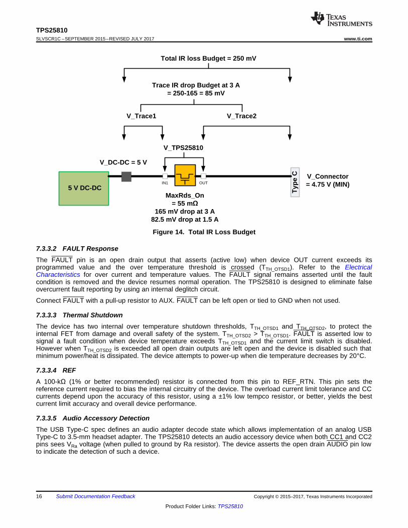
The recommended operating voltage range for IN1/IN2 is 4.5 V to 5.5 V while AUX can be operated from 2.9 Vto 5.5 V. However IN1, the high power supply, can operate up to 6.5 V. This higher input voltage affords a largerIR drop budget in systems where a long cable harness is used and results in high IR drops with 3-A chargingcurrent. Increasing IN1 beyond 5.5 V enables longer cable/board trace lengths between the device and Type Creceptacle while meeting the USB spec for VBUS at connector ≥ 4.75 V.
Figure 14 illustrates the point. In this example IN1 is at 5 V which restricts the IR drop budget from DC-DC toconnector to 250 mV.
V_TPS25810
5 V DC-DC Typ
e C
MaxRds_On= 55 m
165 mV drop at 3 A82.5 mV drop at 1.5 A
V_DC-DC = 5 V
V_Connector= 4.75 V (MIN)
V_Trace1 V_Trace2
IN1 OUT
Total IR loss Budget = 250 mV
Trace IR drop Budget at 3 A = 250-165 = 85 mV
16
TPS25810SLVSCR1C –SEPTEMBER 2015–REVISED JULY 2017 www.ti.com
Product Folder Links: TPS25810
Submit Documentation Feedback Copyright © 2015–2017, Texas Instruments Incorporated
Figure 14. Total IR Loss Budget
7.3.3.2 FAULT ResponseThe FAULT pin is an open drain output that asserts (active low) when device OUT current exceeds itsprogrammed value and the over temperature threshold is crossed (TTH_OTSD1). Refer to the ElectricalCharacteristics for over current and temperature values. The FAULT signal remains asserted until the faultcondition is removed and the device resumes normal operation. The TPS25810 is designed to eliminate falseovercurrent fault reporting by using an internal deglitch circuit.
Connect FAULT with a pull-up resistor to AUX. FAULT can be left open or tied to GND when not used.
7.3.3.3 Thermal ShutdownThe device has two internal over temperature shutdown thresholds, TTH_OTSD1 and TTH_OTSD2, to protect theinternal FET from damage and overall safety of the system. TTH_OTSD2 > TTH_OTSD1. FAULT is asserted low tosignal a fault condition when device temperature exceeds TTH_OTSD1 and the current limit switch is disabled.However when TTH_OTSD2 is exceeded all open drain outputs are left open and the device is disabled such thatminimum power/heat is dissipated. The device attempts to power-up when die temperature decreases by 20°C.
7.3.3.4 REFA 100-kΩ (1% or better recommended) resistor is connected from this pin to REF_RTN. This pin sets thereference current required to bias the internal circuitry of the device. The overload current limit tolerance and CCcurrents depend upon the accuracy of this resistor, using a ±1% low tempco resistor, or better, yields the bestcurrent limit accuracy and overall device performance.
7.3.3.5 Audio Accessory DetectionThe USB Type-C spec defines an audio adapter decode state which allows implementation of an analog USBType-C to 3.5-mm headset adapter. The TPS25810 detects an audio accessory device when both CC1 and CC2pins sees VRa voltage (when pulled to ground by Ra resistor). The device asserts the open drain AUDIO pin lowto indicate the detection of such a device.
17
TPS25810www.ti.com SLVSCR1C –SEPTEMBER 2015–REVISED JULY 2017
Product Folder Links: TPS25810
Submit Documentation FeedbackCopyright © 2015–2017, Texas Instruments Incorporated
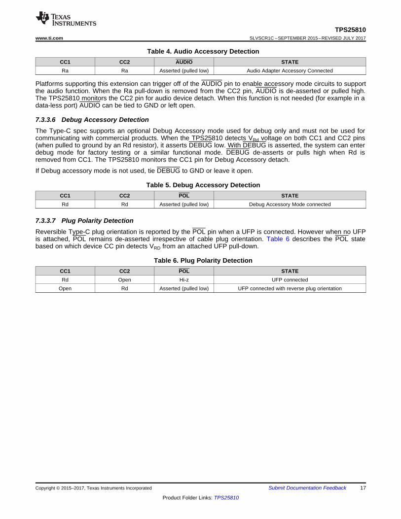
Table 4. Audio Accessory DetectionCC1 CC2 AUDIO STATERa Ra Asserted (pulled low) Audio Adapter Accessory Connected
Platforms supporting this extension can trigger off of the AUDIO pin to enable accessory mode circuits to supportthe audio function. When the Ra pull-down is removed from the CC2 pin, AUDIO is de-asserted or pulled high.The TPS25810 monitors the CC2 pin for audio device detach. When this function is not needed (for example in adata-less port) AUDIO can be tied to GND or left open.
7.3.3.6 Debug Accessory DetectionThe Type-C spec supports an optional Debug Accessory mode used for debug only and must not be used forcommunicating with commercial products. When the TPS25810 detects VRd voltage on both CC1 and CC2 pins(when pulled to ground by an Rd resistor), it asserts DEBUG low. With DEBUG is asserted, the system can enterdebug mode for factory testing or a similar functional mode. DEBUG de-asserts or pulls high when Rd isremoved from CC1. The TPS25810 monitors the CC1 pin for Debug Accessory detach.
If Debug accessory mode is not used, tie DEBUG to GND or leave it open.
Table 5. Debug Accessory DetectionCC1 CC2 POL STATERd Rd Asserted (pulled low) Debug Accessory Mode connected
7.3.3.7 Plug Polarity DetectionReversible Type-C plug orientation is reported by the POL pin when a UFP is connected. However when no UFPis attached, POL remains de-asserted irrespective of cable plug orientation. Table 6 describes the POL statebased on which device CC pin detects VRD from an attached UFP pull-down.
Table 6. Plug Polarity DetectionCC1 CC2 POL STATERd Open Hi-z UFP connected
Open Rd Asserted (pulled low) UFP connected with reverse plug orientation

USB Host
SSTXp
SSTXn
SSRXp
SSRXn
SSRXn1
SSRXp2
SSRXn2
SSTXp1
SSTXn1
SSTXp2
SSTXn2
GND
GND
GND
GND
USB C
SSRXp1
IN1
IN2
AUX
EN
CHG
CHG _HI
REF
OUT
OUT
FAULT
LD_DET
CC1
CC2
UFP
POL
Thermal Pad
GND
REF_RTN
IN1
DEBUG
VB
US
CC
1
CC
2
TPS25810
3.3 V
3.3 V
5 V
5 V
Dp
Dm
Dp
Dm
Dp2
Dm1
Dp
Dm
Dm2
Dp1
AUDIO
A0–
A1+
A1–
OEn
SEL
B0+
B0–
C0+
C0–
B1+
B1–
C1+
C1–
GND
GND
GND
VCC
A0+
HD3SS32120.1 µF
0.1 µF
0.1 µF
0.1 µF
Copyright © 2016, Texas Instruments Incorporated
18
TPS25810SLVSCR1C –SEPTEMBER 2015–REVISED JULY 2017 www.ti.com
Product Folder Links: TPS25810
Submit Documentation Feedback Copyright © 2015–2017, Texas Instruments Incorporated
Figure 15 shows an example implementation which utilizes the POL terminal to control the SEL terminal on theHD3SS3212. The HD3SS3212 provides switching on the differential channels between Port B and Port C to PortA depending on cable orientation.
Figure 15. Example Implementation
7.3.3.8 Device Enable ControlThe logic enable pin controls the power switch and device supply current. The supply current is reduced to lessthan 1 μA when a logic low is present on EN. The EN pin provides a convenient way to turn on or turn off thedevice while it is powered. The enable input threshold has hysteresis built-in. When this pin is pulled high, thedevice is turned on or enabled. When the device is disabled (EN pulled low) the internal FETs tied to IN1 andIN2 are disconnected, all open drain outputs are left open (Hi-Z), and the CC1/CC2 monitor block is turned off.The EN terminal should not be left floating.
7.3.3.9 Load DetectThe load detect function in the device is enabled when it is set to broadcast high current VBUS charging (CHG =CHG_HI = High) on the CC pin. In this mode the device monitors the current to a UFP; if the current exceeds1.95 A (TYP) the LD_DET pin asserts. Since LD_DET is an open drain output, pull it high with 100 kΩ to AUXwhen used; tie it to GND or leave open when not used.
TPS54620Buck
Converter TPS25810#1
LP2950-33LDO
US
B T
ype-
C
Con
nect
or
CHG
CHG_HI
IN1 OUTCC1CC2
/UFP_1
AUX
TPS25810#2 U
SB
Typ
e-C
C
onne
ctor
CHG
CHG_HI
IN1 OUTCC1CC2
/UFP_2
AUX
12V
/UFP_1(High)
/UFP_2(High)
EN
IN2
IN2
No UFP Attached
No UFP Attached
Both /UFP High Converter Disabled
TPS54620Buck
Converter TPS25810#1
LP2950-33LDO
US
B T
ype-
C
Con
nect
or
CHG
CHG_HI
IN1 OUTCC1CC2
/UFP_1
AUX
TPS25810#2 U
SB
Typ
e-C
C
onne
ctor
CHG
CHG_HI
IN1 OUTCC1CC2
/UFP_2
AUX
12V
/UFP_1(Low)
/UFP_2(High)
EN
IN2
IN2
UFPAttached
No UFP Attached
One /UFP Low Converter Enabled
Copyright © 2016, Texas Instruments Incorporated
19
TPS25810www.ti.com SLVSCR1C –SEPTEMBER 2015–REVISED JULY 2017
Product Folder Links: TPS25810
Submit Documentation FeedbackCopyright © 2015–2017, Texas Instruments Incorporated
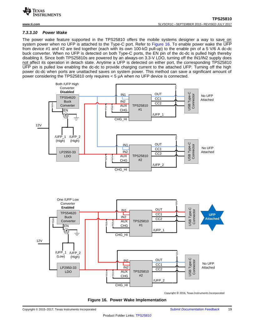
7.3.3.10 Power WakeThe power wake feature supported in the TPS25810 offers the mobile systems designer a way to save onsystem power when no UFP is attached to the Type-C port. Refer to Figure 16. To enable power wake the UFPfrom device #1 and #2 are tied together (each with its own 100-kΩ pull-up) to the enable pin of a 5 V/6 A dc-dcbuck converter. When no UFP is detected on both Type-C ports, the EN pin of the dc-dc is pulled high therebydisabling it. Since both TPS25810s are powered by an always-on 3.3-V LDO, turning off the IN1/IN2 supply doesnot affect its operation in detach state. Anytime a UFP is detected on either port, the corresponding TPS25810UFP pin is pulled low enabling the dc-dc to provide charging current to the attached UFP. Turning off the highpower dc-dc when ports are unattached saves on system power. This method can save a significant amount ofpower considering the TPS25810 only requires < 5 µA when no UFP device is connected.
Figure 16. Power Wake Implementation
TPS54620Buck
Converter TPS25810#1
LP2950-33LDO
US
B T
ype-
C
Con
nect
or
CHG
CHG_HI
IN1 OUTCC1CC2
/LD_DET_1/UFP_1
AUX
TPS25810#2 U
SB
Typ
e-C
C
onne
ctor
CHG
CHG_HI
IN1 OUTCC1CC2
/LD_DET_2/UFP_2
AUX
/UFP_1 /UFP_2
12V
3.0A Broadcast
EN
IN2
IN2
Copyright © 2016, Texas Instruments Incorporated
20
TPS25810SLVSCR1C –SEPTEMBER 2015–REVISED JULY 2017 www.ti.com
Product Folder Links: TPS25810
Submit Documentation Feedback Copyright © 2015–2017, Texas Instruments Incorporated
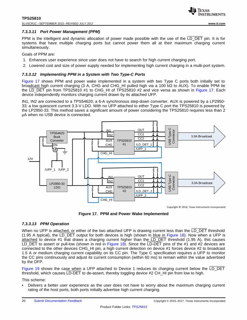
7.3.3.11 Port Power Management (PPM)PPM is the intelligent and dynamic allocation of power made possible with the use of the LD_DET pin. It is forsystems that have multiple charging ports but cannot power them all at their maximum charging currentsimultaneously.
Goals of PPM are:1. Enhances user experience since user does not have to search for high current charging port.2. Lowered cost and size of power supply needed for implementing high current charging in a multi-port system.
7.3.3.12 Implementing PPM in a System with Two Type-C PortsFigure 17 shows PPM and power wake implemented in a system with two Type C ports both initially set tobroadcast high current charging (3 A, CHG and CHG_HI pulled high via a 100 kΩ to AUX). To enable PPM tiethe LD_DET pin from TPS25810 #1 to CHG_HI of TPS25810 #2 and vice versa as shown in Figure 17. Eachdevice independently monitors charging current drawn by its attached UFP.
IN1, IN2 are connected to a TPS54620; a 6-A synchronous step-down converter. AUX is powered by a LP2950-33; a low quiescent current 3.3-V LDO. With no UFP attached to either Type C port the TPS25810 is powered bythe LP2950-33. This method saves a significant amount of power considering the TPS25810 requires less than 2µA when no USB device is connected.
Figure 17. PPM and Power Wake Implemented
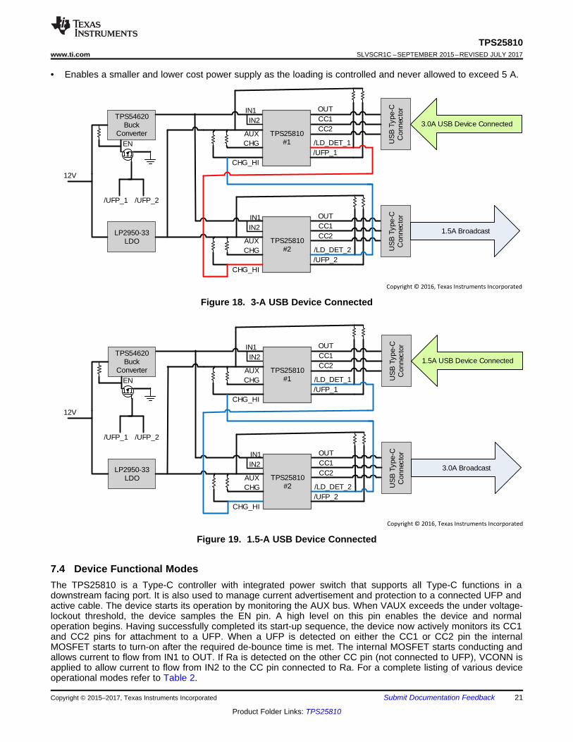
7.3.3.13 PPM OperationWhen no UFP is attached, or either of the two attached UFP is drawing current less than the LD_DET threshold(1.95 A typical), the LD_DET output for both devices is high (shown in blue in Figure 18). Now when a UFP isattached to device #1 that draws a charging current higher than the LD_DET threshold (1.95 A), this causesLD_DET to assert or pull-low (shown in red in Figure 18). Since the LD-DET pins of the #1 and #2 devices areconnected to the other devices CHG_HI pin, a high current detection on device #1 forces device #2 to broadcast1.5 A or medium charging current capability on its CC pin. The Type C specification requires a UFP to monitorthe CC pins continuously and adjust its current consumption (within 60 ms) to remain within the value advertisedby the DFP.
Figure 19 shows the case when a UFP attached to Device 1 reduces its charging current below the LD_DETthreshold, which causes LD-DET to de-assert, thereby toggling device #2 CH_HI pin from low to high.
This scheme:• Delivers a better user experience as the user does not have to worry about the maximum charging current
rating of the host ports, both ports initially advertise high current charging.
TPS54620Buck
Converter TPS25810#1
LP2950-33LDO
US
B T
ype-
C
Con
nect
or
CHG
CHG_HI
IN1 OUTCC1CC2
/LD_DET_1/UFP_1
AUX
TPS25810#2 U
SB
Typ
e-C
C
onne
ctor
CHG
CHG_HI
IN1 OUTCC1CC2
/LD_DET_2/UFP_2
AUX
12V
3.0A Broadcast
1.5A USB Device Connected
/UFP_1 /UFP_2
EN
IN2
IN2
Copyright © 2016, Texas Instruments Incorporated
TPS54620Buck
Converter TPS25810#1
LP2950-33LDO
US
B T
ype-
C
Con
nect
or
CHG
CHG_HI
IN1 OUTCC1CC2
/LD_DET_1/UFP_1
AUX
TPS25810#2 U
SB
Typ
e-C
C
onne
ctor
CHG
CHG_HI
IN1 OUTCC1CC2
/LD_DET_2/UFP_2
AUX
12V
1.5A Broadcast
3.0A USB Device Connected
/UFP_1 /UFP_2
EN
IN2
IN2
Copyright © 2016, Texas Instruments Incorporated
21
TPS25810www.ti.com SLVSCR1C –SEPTEMBER 2015–REVISED JULY 2017
Product Folder Links: TPS25810
Submit Documentation FeedbackCopyright © 2015–2017, Texas Instruments Incorporated
• Enables a smaller and lower cost power supply as the loading is controlled and never allowed to exceed 5 A.
Figure 18. 3-A USB Device Connected
Figure 19. 1.5-A USB Device Connected
7.4 Device Functional ModesThe TPS25810 is a Type-C controller with integrated power switch that supports all Type-C functions in adownstream facing port. It is also used to manage current advertisement and protection to a connected UFP andactive cable. The device starts its operation by monitoring the AUX bus. When VAUX exceeds the under voltage-lockout threshold, the device samples the EN pin. A high level on this pin enables the device and normaloperation begins. Having successfully completed its start-up sequence, the device now actively monitors its CC1and CC2 pins for attachment to a UFP. When a UFP is detected on either the CC1 or CC2 pin the internalMOSFET starts to turn-on after the required de-bounce time is met. The internal MOSFET starts conducting andallows current to flow from IN1 to OUT. If Ra is detected on the other CC pin (not connected to UFP), VCONN isapplied to allow current to flow from IN2 to the CC pin connected to Ra. For a complete listing of various deviceoperational modes refer to Table 2.
IN1
IN2
AUX
EN
CHGCHG_HI
REF
REF_RTN PAD
GND
DEBUGAUDIO
POLUFP
LD_DETFAULT
CC2
CC1
OUT
OUT
2
3
4
5
6
78
10
9 21
12
16
171819201
1113
15
14
TPS25810RVC
100 N(1%)
USB Type CReceptacle
47uF
10uF
5VVBUS
47uF
47uF
0.1u
F
IN1
Copyright © 2016, Texas Instruments Incorporated
22
TPS25810SLVSCR1C –SEPTEMBER 2015–REVISED JULY 2017 www.ti.com
Product Folder Links: TPS25810
Submit Documentation Feedback Copyright © 2015–2017, Texas Instruments Incorporated
8 Application and Implementation
NOTEInformation in the following applications sections is not part of the TI componentspecification, and TI does not warrant its accuracy or completeness. TI’s customers areresponsible for determining suitability of components for their purposes. Customers shouldvalidate and test their design implementation to confirm system functionality.
8.1 Application InformationThe TPS25810 is a Type-C DFP controller that supports all Type-C DFP required functions. The TPS25810 onlyapplies power to VBUS when it detects that a UFP is attached and removes power when it detects the UFP isdetached. The device exposes its identity via its CC pin advertising its current capability based on CHG andCHG_HI pin settings. The TPS25810 also limits its advertised current internally and provides robust protection toa fault on the system VBUS power rail.
After a connection is established by the TPS25810, the device is capable of providing VCONN to power circuits inthe cable plug on the CC pin that is not connected to the CC wire in the cable. VCONN is internally current limitedand has its own supply pin IN2. Apart from providing charging current to a UFP, the TPS25810 also supportsAudio and Debug accessory modes.
The following design procedure can be used to implement a full featured Type-C DFP.
NOTEBC 1.2 is not supported in the TPS25810. To support BC1.2 with Type-C charging modesin a single C connector, a device like a TPS2514A will need to be used.
8.2 Typical Applications
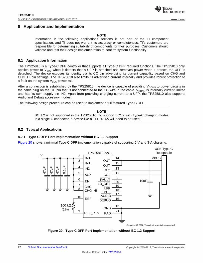
8.2.1 Type C DFP Port Implementation without BC 1.2 SupportFigure 20 shows a minimal Type-C DFP implementation capable of supporting 5-V and 3-A charging.
Figure 20. Type-C DFP Port Implementation without BC 1.2 Support

23
TPS25810www.ti.com SLVSCR1C –SEPTEMBER 2015–REVISED JULY 2017
Product Folder Links: TPS25810
Submit Documentation FeedbackCopyright © 2015–2017, Texas Instruments Incorporated
Typical Applications (continued)8.2.1.1 Design Requirements
8.2.1.1.1 Input and Output Capacitance
Input and output capacitance improves the performance of the device. The actual capacitance should beoptimized for the particular application. For all applications, a 0.1-μF or greater ceramic bypass capacitorbetween IN and GND is recommended as close to the device as possible for local noise de-coupling.
All protection circuits such as the TPS25810 have the potential for input voltage overshoots and output voltageundershoots. Input voltage overshoots can be caused by either of two effects. The first cause is an abruptapplication of input voltage in conjunction with input power bus inductance and input capacitance when the INterminal is high impedance (before turn on). Theoretically, the peak voltage is 2 times the applied. The secondcause is due to the abrupt reduction of output short circuit current when the TPS25810 turns off and energystored in the input inductance drives the input voltage high. Input voltage droops may also occur with large loadsteps and as the TPS25810 output is shorted. Applications with large input inductance (for instance connectingthe evaluation board to the bench power-supply through long cables) may require large input capacitance toreduce the voltage overshoot from exceeding the absolute maximum voltage of the device.
The fast current-limit speed of the TPS25810 to hard output short circuits isolate the input bus form faults.However, ceramic input capacitance in the range of 1 μF to 22 μF adjacent to the TPS25810 input aids in bothresponse time and limiting the transient seen on the input power bus. Momentary input transients to 6.5 V arepermitted. Output voltage undershoot is caused by the inductance of the output power bus just after a short hasoccurred and the TPS25810 has abruptly reduced OUT current. Energy stored in the inductance drives the OUTvoltage down and potentially negative as it discharges. An application with large output inductance (such as froma cable) benefits from use of a high-value output capacitor to control voltage undershoot.
When implementing a USB standard application, 120 μF minimum output capacitance is required. Typically a150-μF electrolytic capacitor is used, which is sufficient to control voltage undershoots. Since in Type-C DFP is acold socket when no UFP is attached, the output capacitance should be placed at the IN pin versus OUT as isused in USB Type A ports. It is also recommended to put a 10-μF ceramic capacitor on the OUT pin for bettervoltage bypass.
8.2.1.2 Detailed Design ProcedureThe TPS25810 device supports three different input voltages based on the application. In the simplestimplementation all input supplies are tied to a single voltage source as shown in Figure 20 which is set to 5 V.However, it is recommended to set a slightly higher (100 mV to 200 mV) input voltage, when possible, tocompensate for IR drop from the source to the Type C connector.
Other design considerations are listed below:• Place at least 120 µF of bypass capacitance close to the IN pins versus OUT as Type C is a cold socket
connector.• A 10-µF bypass capacitor is recommended placed near a Type-C receptacle VBUS pin to handle load
transients.• Depending on the max current level advertisement supported by the Type-C port in the system, set CHG and
CHG_HI levels accordingly. 3 A advertisement is shown in Figure 20.• EN, CHG, and CHG_HI pins can be tied directly to GND or VAUX without a pull-up resistor.
– CHG and CHG_HI can also be dynamically controlled by a µC to change the current advertisement levelto the UFP.
• When an open drain output of the TPS25810 is not used, it can be left as NC or tied to GND.• Use a 1% 100-kΩ resistor to connect between the REF and REF_RTN pins placing it close to the device pin
and isolated from switching noise on the board.
Time 20 ms/div
2A
/div
2 V
/div
2 V
/div
2 V
/div
VBUS
CC1
VIN
IN
Time 20 ms/div
2 V
/div
2 V
/div
2 V
/div
2 V
/div
VOUT
CC1
VIN
CC2
Time 200 s/divm
50
0 m
A/d
iv2
V/d
iv2
V/d
iv
2 V
/div
VBUS
CC1
VIN
IN
Time 50 ms/div
2A
/div
2 V
/div
2 V
/div
2 V
/div
VBUS
CC1
VIN
IN
Time 50 ms/div
2 V
/div
2 V
/div
2 V
/div
2 V
/div
VBUS
CC1
VIN
CC2
Time 20 ms/div
2 V
/div
2 V
/div
2 V
/div
2A
/divIN
VBUS
CC1
VIN
24
TPS25810SLVSCR1C –SEPTEMBER 2015–REVISED JULY 2017 www.ti.com
Product Folder Links: TPS25810
Submit Documentation Feedback Copyright © 2015–2017, Texas Instruments Incorporated
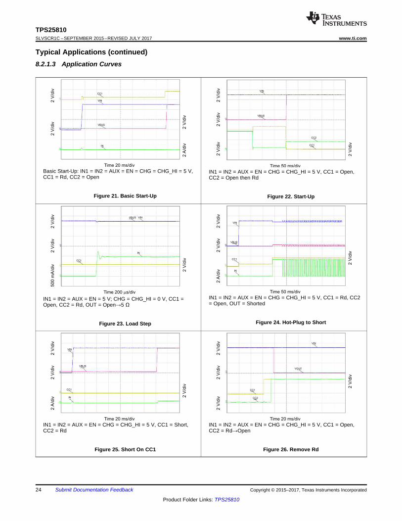
Typical Applications (continued)8.2.1.3 Application Curves
Basic Start-Up: IN1 = IN2 = AUX = EN = CHG = CHG_HI = 5 V,CC1 = Rd, CC2 = Open
Figure 21. Basic Start-Up
IN1 = IN2 = AUX = EN = CHG = CHG_HI = 5 V, CC1 = Open,CC2 = Open then Rd
Figure 22. Start-Up
IN1 = IN2 = AUX = EN = 5 V; CHG = CHG_HI = 0 V, CC1 =Open, CC2 = Rd, OUT = Open→5 Ω
Figure 23. Load Step
IN1 = IN2 = AUX = EN = CHG = CHG_HI = 5 V, CC1 = Rd, CC2= Open, OUT = Shorted
Figure 24. Hot-Plug to Short
IN1 = IN2 = AUX = EN = CHG = CHG_HI = 5 V, CC1 = Short,CC2 = Rd
Figure 25. Short On CC1
IN1 = IN2 = AUX = EN = CHG = CHG_HI = 5 V, CC1 = Open,CC2 = Rd→Open
Figure 26. Remove Rd
Time 50 ms/div
2 V
/div
2 V
/div
2 V
/div
2 V
/div
VBUS
CC1
VIN
CC2
25
TPS25810www.ti.com SLVSCR1C –SEPTEMBER 2015–REVISED JULY 2017
Product Folder Links: TPS25810
Submit Documentation FeedbackCopyright © 2015–2017, Texas Instruments Incorporated
Typical Applications (continued)
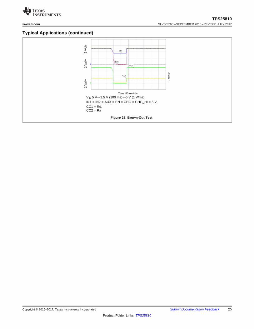
VIN 5 V→3.5 V (100 ms)→5 V (1 V/ms),IN1 = IN2 = AUX = EN = CHG = CHG_HI = 5 V,CC1 = Rd,CC2 = Ra
Figure 27. Brown-Out Test
IN1
IN1
IN2
AUX
EN
CHGCHG_HI
REF
REF_RTN PAD
GND
DEBUGAUDIO
POLUFP
LD_DETFAULT
CC2
CC1
OUT
OUT
2
3
4
5
6
78
10
9 21
12
16
171819201
1113
15
14
TPS25810RVC
100 N(1%)
USB Type CReceptacle
47uF
10uF
5VVBUS
DM1
DP1
IN
GNDNCNC
TPS2514ADBV
0.1uF
DnDp
47uF
47uF
0.1u
F
Copyright © 2016, Texas Instruments Incorporated
26
TPS25810SLVSCR1C –SEPTEMBER 2015–REVISED JULY 2017 www.ti.com
Product Folder Links: TPS25810
Submit Documentation Feedback Copyright © 2015–2017, Texas Instruments Incorporated
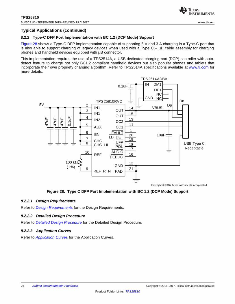
Typical Applications (continued)8.2.2 Type-C DFP Port Implementation with BC 1.2 (DCP Mode) SupportFigure 28 shows a Type-C DFP implementation capable of supporting 5 V and 3 A charging in a Type-C port thatis also able to support charging of legacy devices when used with a Type C – µB cable assembly for chargingphones and handheld devices equipped with µB connector.
This implementation requires the use of a TPS2514A, a USB dedicated charging port (DCP) controller with auto-detect feature to charge not only BC1.2 compliant handheld devices but also popular phones and tablets thatincorporate their own propriety charging algorithm. Refer to TPS2514A specifications available at www.ti.com formore details.
Figure 28. Type C DFP Port Implementation with BC 1.2 (DCP Mode) Support
8.2.2.1 Design RequirementsRefer to Design Requirements for the Design Requirements.
8.2.2.2 Detailed Design ProcedureRefer to Detailed Design Procedure for the Detailed Design Procedure.
8.2.2.3 Application CurvesRefer to Application Curves for the Application Curves.

27
TPS25810www.ti.com SLVSCR1C –SEPTEMBER 2015–REVISED JULY 2017
Product Folder Links: TPS25810
Submit Documentation FeedbackCopyright © 2015–2017, Texas Instruments Incorporated
9 Power Supply RecommendationsThe device has three power supply inputs; IN1, which is directly connected to OUT via the power MOSFET, istied to the VBUS pin in the Type-C receptacle. IN2 also has a current limiting switch and is MUXed either to theCC1 or CC2 pin in the Type-C receptacle depending on cable plug polarity. AUX is the chip supply. In mostapplications all three supplies are tied together. In a special implementation like power wake IN1/IN2 are tied to asingle supply while AUX is powered by a supply that is always ON and can be as low as 2.9 V.
USB Specification Revisions 2.0 and 3.1 require VBUS voltage at the connector to be between 4.75 V to 5.5 V.Depending on layout and routing from supply to the connector the voltage droop on VBUS has to be tightlycontrolled. Locate the input supply close to the device. For all applications, a 10-μF or greater ceramic bypasscapacitor between OUT and GND is recommended as close to the Type-C connector of the device as possiblefor local noise decoupling. The power supply should be rated higher than the current limit set to avoid voltagedroops during over current and short-circuit conditions.
28
TPS25810SLVSCR1C –SEPTEMBER 2015–REVISED JULY 2017 www.ti.com
Product Folder Links: TPS25810
Submit Documentation Feedback Copyright © 2015–2017, Texas Instruments Incorporated
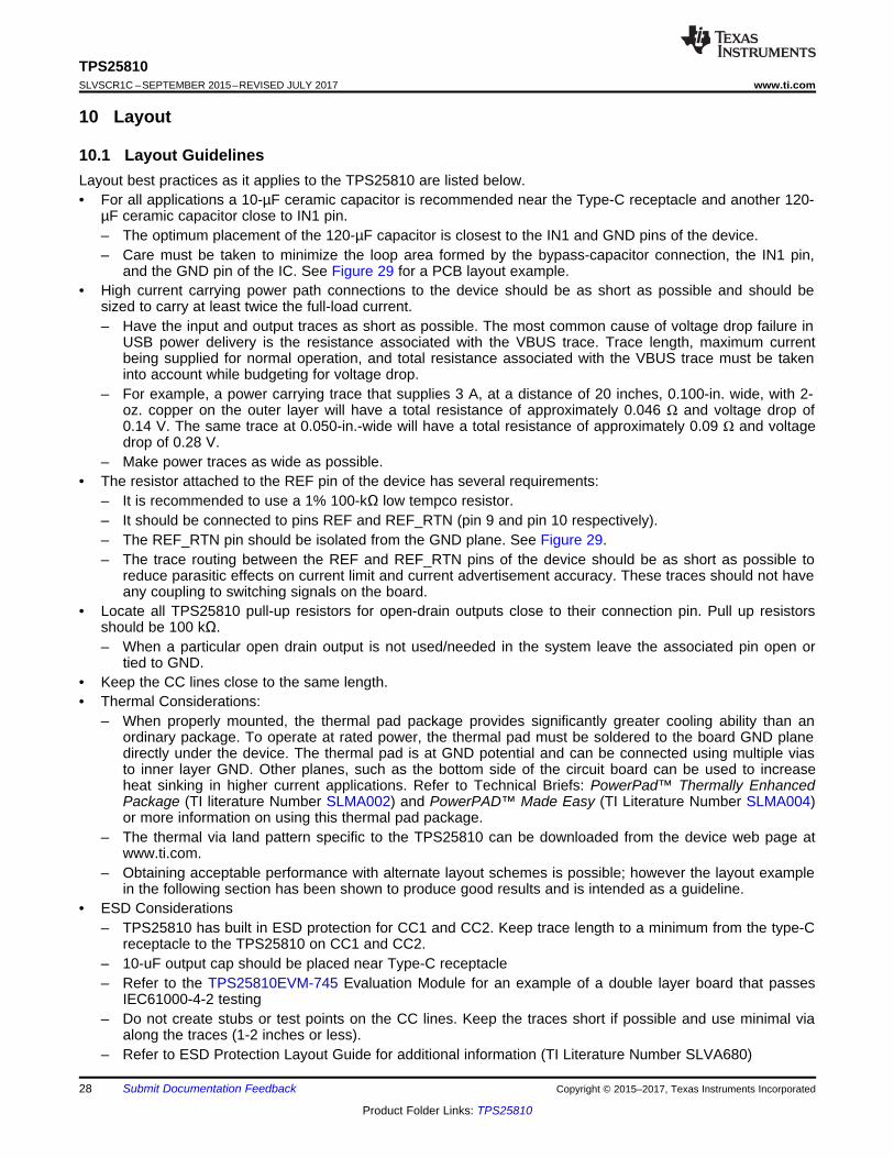
10 Layout
10.1 Layout GuidelinesLayout best practices as it applies to the TPS25810 are listed below.• For all applications a 10-µF ceramic capacitor is recommended near the Type-C receptacle and another 120-
µF ceramic capacitor close to IN1 pin.– The optimum placement of the 120-µF capacitor is closest to the IN1 and GND pins of the device.– Care must be taken to minimize the loop area formed by the bypass-capacitor connection, the IN1 pin,
and the GND pin of the IC. See Figure 29 for a PCB layout example.• High current carrying power path connections to the device should be as short as possible and should be
sized to carry at least twice the full-load current.– Have the input and output traces as short as possible. The most common cause of voltage drop failure in
USB power delivery is the resistance associated with the VBUS trace. Trace length, maximum currentbeing supplied for normal operation, and total resistance associated with the VBUS trace must be takeninto account while budgeting for voltage drop.
– For example, a power carrying trace that supplies 3 A, at a distance of 20 inches, 0.100-in. wide, with 2-oz. copper on the outer layer will have a total resistance of approximately 0.046 Ω and voltage drop of0.14 V. The same trace at 0.050-in.-wide will have a total resistance of approximately 0.09 Ω and voltagedrop of 0.28 V.
– Make power traces as wide as possible.• The resistor attached to the REF pin of the device has several requirements:
– It is recommended to use a 1% 100-kΩ low tempco resistor.– It should be connected to pins REF and REF_RTN (pin 9 and pin 10 respectively).– The REF_RTN pin should be isolated from the GND plane. See Figure 29.– The trace routing between the REF and REF_RTN pins of the device should be as short as possible to
reduce parasitic effects on current limit and current advertisement accuracy. These traces should not haveany coupling to switching signals on the board.
• Locate all TPS25810 pull-up resistors for open-drain outputs close to their connection pin. Pull up resistorsshould be 100 kΩ.– When a particular open drain output is not used/needed in the system leave the associated pin open or
tied to GND.• Keep the CC lines close to the same length.• Thermal Considerations:
– When properly mounted, the thermal pad package provides significantly greater cooling ability than anordinary package. To operate at rated power, the thermal pad must be soldered to the board GND planedirectly under the device. The thermal pad is at GND potential and can be connected using multiple viasto inner layer GND. Other planes, such as the bottom side of the circuit board can be used to increaseheat sinking in higher current applications. Refer to Technical Briefs: PowerPad™ Thermally EnhancedPackage (TI literature Number SLMA002) and PowerPAD™ Made Easy (TI Literature Number SLMA004)or more information on using this thermal pad package.
– The thermal via land pattern specific to the TPS25810 can be downloaded from the device web page atwww.ti.com.
– Obtaining acceptable performance with alternate layout schemes is possible; however the layout examplein the following section has been shown to produce good results and is intended as a guideline.
• ESD Considerations– TPS25810 has built in ESD protection for CC1 and CC2. Keep trace length to a minimum from the type-C
receptacle to the TPS25810 on CC1 and CC2.– 10-uF output cap should be placed near Type-C receptacle– Refer to the TPS25810EVM-745 Evaluation Module for an example of a double layer board that passes
IEC61000-4-2 testing– Do not create stubs or test points on the CC lines. Keep the traces short if possible and use minimal via
along the traces (1-2 inches or less).– Refer to ESD Protection Layout Guide for additional information (TI Literature Number SLVA680)
1
2
3
4
5
6
7 8 9 10
11
12
13
14
15
16
17181920
xxxxxxxxxxxxxxxxxxxxxxxxxxxxxxxxxxxx
xxxxxxxxxxxxxxxxxxxxxxxxxxxxxx
xxxxxxxxxxxxxxxxxxxxxxxxxxxxxx
xxxxxxxxxxxxxxxxxxxxxxxxxxxxxxxxxxxx
xxxxxxxxxxxxxxxxxxxxxxxxxxxxxxxxxxxx
IN1
IN2
AUX
AUX
EN
CH
G
CH
G_H
I
RE
F_RTN
RE
F
CC1
CC2
GND
ThermalPad
OUT
/DE
BU
G
/AU
DIO
/PO
L
/UFP
/LD_D
ET
/FA
ULT
Signal GroundTop Layer
Signal GroundBottom Layer
Bottom Layer Signal Trace
Top Layer Signal Trace
Top Layer Signal Ground Plane
Bottom Layer Signal Ground Plane
Via to Bottom Layer Signal Ground Plane
xxxxxxxxxxxxxxxxxxxxxxxxxxxxxxxxxxxx Via to Bottom Layer Signal
xxxxxxxxxxxxxxxxxxxxxxxxxxxxxxxxxxxx
xxxxxxxxxxxxxxxxxxxxxxxxxxxxxxxxxxxx
xxxxxxxxxxxxxxxxxxxxxxxxxxxxxx
xxxxxxxxxxxxxxxxxxxxxxxxxxxxxxxxxxxx
xxxxxxxxxxxxxxxxxxxxxxxxxxxxxxxxxxxx
xxxxxxxxxxxxxxxxxxxxxxxxxxxxxxxxxxxx
29
TPS25810www.ti.com SLVSCR1C –SEPTEMBER 2015–REVISED JULY 2017
Product Folder Links: TPS25810
Submit Documentation FeedbackCopyright © 2015–2017, Texas Instruments Incorporated
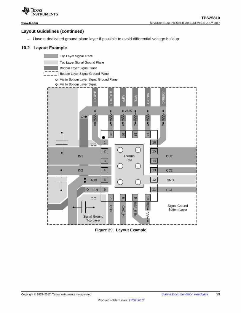
Layout Guidelines (continued)– Have a dedicated ground plane layer if possible to avoid differential voltage buildup
10.2 Layout Example
Figure 29. Layout Example
30
TPS25810SLVSCR1C –SEPTEMBER 2015–REVISED JULY 2017 www.ti.com
Product Folder Links: TPS25810
Submit Documentation Feedback Copyright © 2015–2017, Texas Instruments Incorporated
11 Device and Documentation Support
11.1 Device Support
11.1.1 Third-Party Products DisclaimerTI'S PUBLICATION OF INFORMATION REGARDING THIRD-PARTY PRODUCTS OR SERVICES DOES NOTCONSTITUTE AN ENDORSEMENT REGARDING THE SUITABILITY OF SUCH PRODUCTS OR SERVICESOR A WARRANTY, REPRESENTATION OR ENDORSEMENT OF SUCH PRODUCTS OR SERVICES, EITHERALONE OR IN COMBINATION WITH ANY TI PRODUCT OR SERVICE.
11.2 Documentation Support
11.2.1 Related DocumentationPowerPad™ Thermally Enhanced Package (TI literature Number SLMA002)
PowerPAD™ Made Easy (TI Literature Number SLMA004)
TPS25810EVM-745 User's Guide (SLVUAI0)
Protecting the TPS25810 from High Voltage DFPs (SLVA751)
11.3 Receiving Notification of Documentation UpdatesTo receive notification of documentation updates, navigate to the device product folder on ti.com. In the upperright corner, click on Alert me to register and receive a weekly digest of any product information that haschanged. For change details, review the revision history included in any revised document.
11.4 Community ResourcesThe following links connect to TI community resources. Linked contents are provided "AS IS" by the respectivecontributors. They do not constitute TI specifications and do not necessarily reflect TI's views; see TI's Terms ofUse.
TI E2E™ Online Community TI's Engineer-to-Engineer (E2E) Community. Created to foster collaborationamong engineers. At e2e.ti.com, you can ask questions, share knowledge, explore ideas and helpsolve problems with fellow engineers.
Design Support TI's Design Support Quickly find helpful E2E forums along with design support tools andcontact information for technical support.
11.5 TrademarksE2E is a trademark of Texas Instruments.All other trademarks are the property of their respective owners.
11.6 Electrostatic Discharge CautionThese devices have limited built-in ESD protection. The leads should be shorted together or the device placed in conductive foamduring storage or handling to prevent electrostatic damage to the MOS gates.
11.7 GlossarySLYZ022 — TI Glossary.
This glossary lists and explains terms, acronyms, and definitions.
12 Mechanical, Packaging, and Orderable InformationThe following pages include mechanical, packaging, and orderable information. This information is the mostcurrent data available for the designated devices. This data is subject to change without notice and revision ofthis document. For browser-based versions of this data sheet, refer to the left-hand navigation.
PACKAGE OPTION ADDENDUM
www.ti.com 22-Nov-2016
Addendum-Page 1
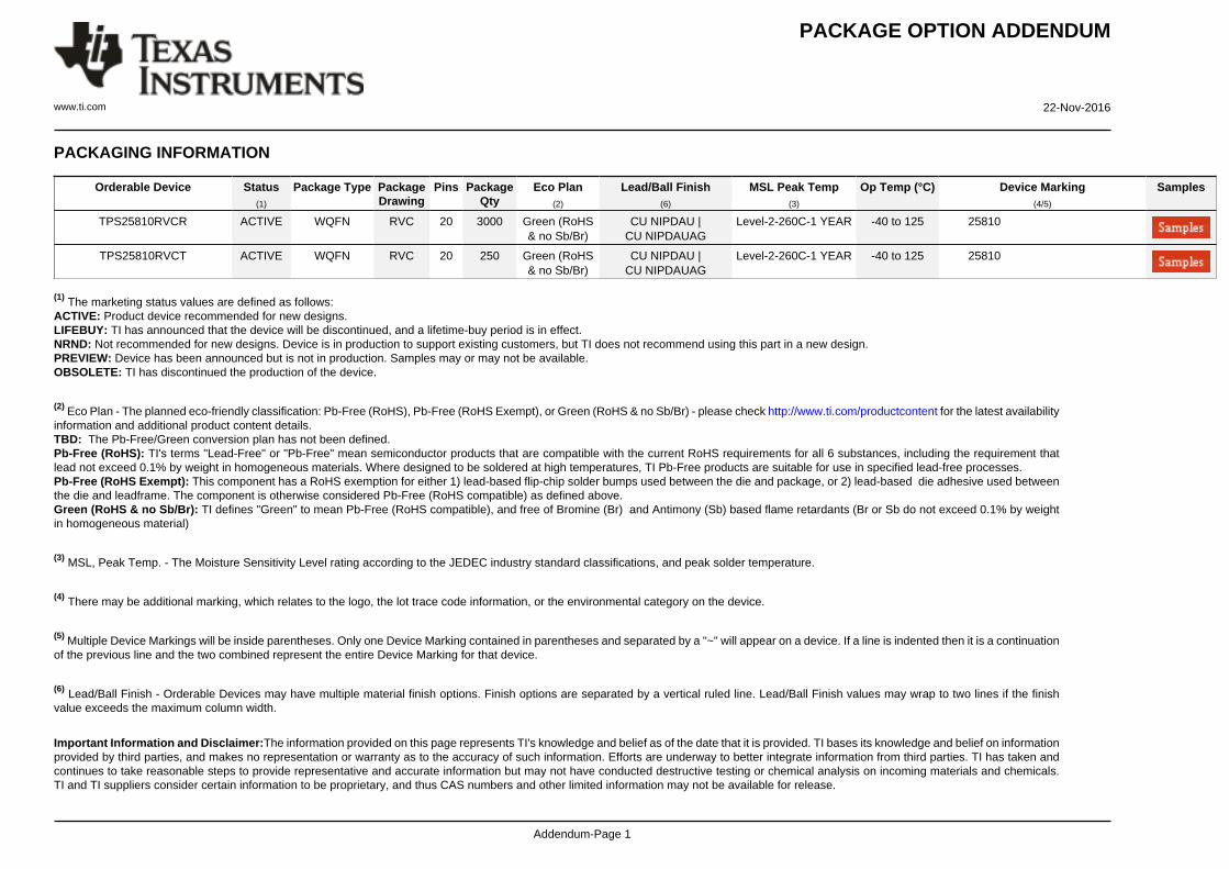
PACKAGING INFORMATION
Orderable Device Status(1)
Package Type PackageDrawing
Pins PackageQty
Eco Plan(2)
Lead/Ball Finish(6)
MSL Peak Temp(3)
Op Temp (°C) Device Marking(4/5)
Samples
TPS25810RVCR ACTIVE WQFN RVC 20 3000 Green (RoHS& no Sb/Br)
CU NIPDAU |CU NIPDAUAG
Level-2-260C-1 YEAR -40 to 125 25810
TPS25810RVCT ACTIVE WQFN RVC 20 250 Green (RoHS& no Sb/Br)
CU NIPDAU |CU NIPDAUAG
Level-2-260C-1 YEAR -40 to 125 25810
(1) The marketing status values are defined as follows:ACTIVE: Product device recommended for new designs.LIFEBUY: TI has announced that the device will be discontinued, and a lifetime-buy period is in effect.NRND: Not recommended for new designs. Device is in production to support existing customers, but TI does not recommend using this part in a new design.PREVIEW: Device has been announced but is not in production. Samples may or may not be available.OBSOLETE: TI has discontinued the production of the device.
(2) Eco Plan - The planned eco-friendly classification: Pb-Free (RoHS), Pb-Free (RoHS Exempt), or Green (RoHS & no Sb/Br) - please check http://www.ti.com/productcontent for the latest availabilityinformation and additional product content details.TBD: The Pb-Free/Green conversion plan has not been defined.Pb-Free (RoHS): TI's terms "Lead-Free" or "Pb-Free" mean semiconductor products that are compatible with the current RoHS requirements for all 6 substances, including the requirement thatlead not exceed 0.1% by weight in homogeneous materials. Where designed to be soldered at high temperatures, TI Pb-Free products are suitable for use in specified lead-free processes.Pb-Free (RoHS Exempt): This component has a RoHS exemption for either 1) lead-based flip-chip solder bumps used between the die and package, or 2) lead-based die adhesive used betweenthe die and leadframe. The component is otherwise considered Pb-Free (RoHS compatible) as defined above.Green (RoHS & no Sb/Br): TI defines "Green" to mean Pb-Free (RoHS compatible), and free of Bromine (Br) and Antimony (Sb) based flame retardants (Br or Sb do not exceed 0.1% by weightin homogeneous material)
(3) MSL, Peak Temp. - The Moisture Sensitivity Level rating according to the JEDEC industry standard classifications, and peak solder temperature.
(4) There may be additional marking, which relates to the logo, the lot trace code information, or the environmental category on the device.
(5) Multiple Device Markings will be inside parentheses. Only one Device Marking contained in parentheses and separated by a "~" will appear on a device. If a line is indented then it is a continuationof the previous line and the two combined represent the entire Device Marking for that device.
(6) Lead/Ball Finish - Orderable Devices may have multiple material finish options. Finish options are separated by a vertical ruled line. Lead/Ball Finish values may wrap to two lines if the finishvalue exceeds the maximum column width.
Important Information and Disclaimer:The information provided on this page represents TI's knowledge and belief as of the date that it is provided. TI bases its knowledge and belief on informationprovided by third parties, and makes no representation or warranty as to the accuracy of such information. Efforts are underway to better integrate information from third parties. TI has taken andcontinues to take reasonable steps to provide representative and accurate information but may not have conducted destructive testing or chemical analysis on incoming materials and chemicals.TI and TI suppliers consider certain information to be proprietary, and thus CAS numbers and other limited information may not be available for release.
PACKAGE OPTION ADDENDUM
www.ti.com 22-Nov-2016
Addendum-Page 2
In no event shall TI's liability arising out of such information exceed the total purchase price of the TI part(s) at issue in this document sold by TI to Customer on an annual basis.
OTHER QUALIFIED VERSIONS OF TPS25810 :
• Automotive: TPS25810-Q1
NOTE: Qualified Version Definitions:
• Automotive - Q100 devices qualified for high-reliability automotive applications targeting zero defects
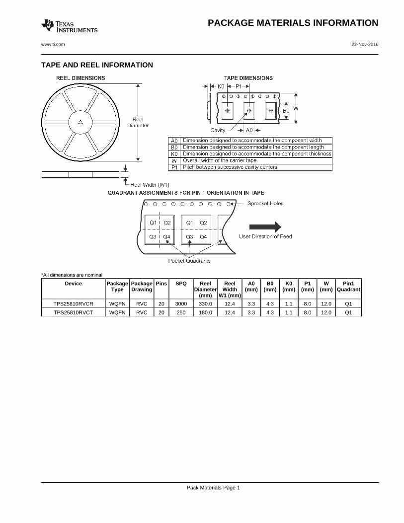
TAPE AND REEL INFORMATION
*All dimensions are nominal
Device PackageType
PackageDrawing
Pins SPQ ReelDiameter
(mm)
ReelWidth
W1 (mm)
A0(mm)
B0(mm)
K0(mm)
P1(mm)
W(mm)
Pin1Quadrant
TPS25810RVCR WQFN RVC 20 3000 330.0 12.4 3.3 4.3 1.1 8.0 12.0 Q1
TPS25810RVCT WQFN RVC 20 250 180.0 12.4 3.3 4.3 1.1 8.0 12.0 Q1
PACKAGE MATERIALS INFORMATION
www.ti.com 22-Nov-2016
Pack Materials-Page 1
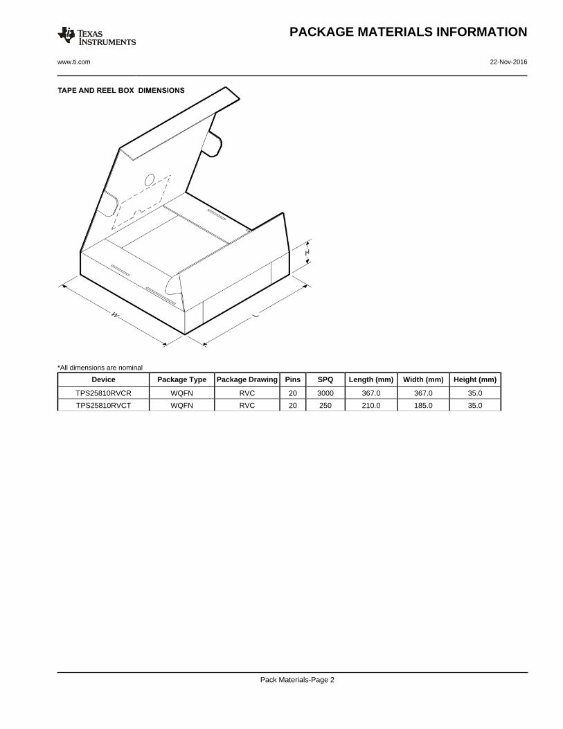
*All dimensions are nominal
Device Package Type Package Drawing Pins SPQ Length (mm) Width (mm) Height (mm)
TPS25810RVCR WQFN RVC 20 3000 367.0 367.0 35.0
TPS25810RVCT WQFN RVC 20 250 210.0 185.0 35.0
PACKAGE MATERIALS INFORMATION
www.ti.com 22-Nov-2016
Pack Materials-Page 2


www.ti.com
PACKAGE OUTLINE
C
SEE TERMINALDETAIL
20X 0.250.15
1.6 0.1
20X 0.450.35
0.8 MAX
(0.2) TYP
0.050.00
16X 0.5
2X2.5
2X 1.5
2.6 0.1
B 3.12.9
A
4.13.9
0.250.15
0.450.35
WQFN - 0.8 mm max heightRVC0020APLASTIC QUAD FLATPACK - NO LEAD
4219150/B 03/2017
PIN 1 INDEX AREA
0.08
SEATING PLANE
1
6 11
16
7 10
20 17(OPTIONAL)
PIN 1 ID 0.1 C A B0.05
EXPOSEDTHERMAL PAD
21 SYMM
SYMM
NOTES: 1. All linear dimensions are in millimeters. Any dimensions in parenthesis are for reference only. Dimensioning and tolerancing per ASME Y14.5M. 2. This drawing is subject to change without notice. 3. The package thermal pad must be soldered to the printed circuit board for optimal thermal and mechanical performance.
SCALE 3.700
DETAILOPTIONAL TERMINAL
TYPICAL
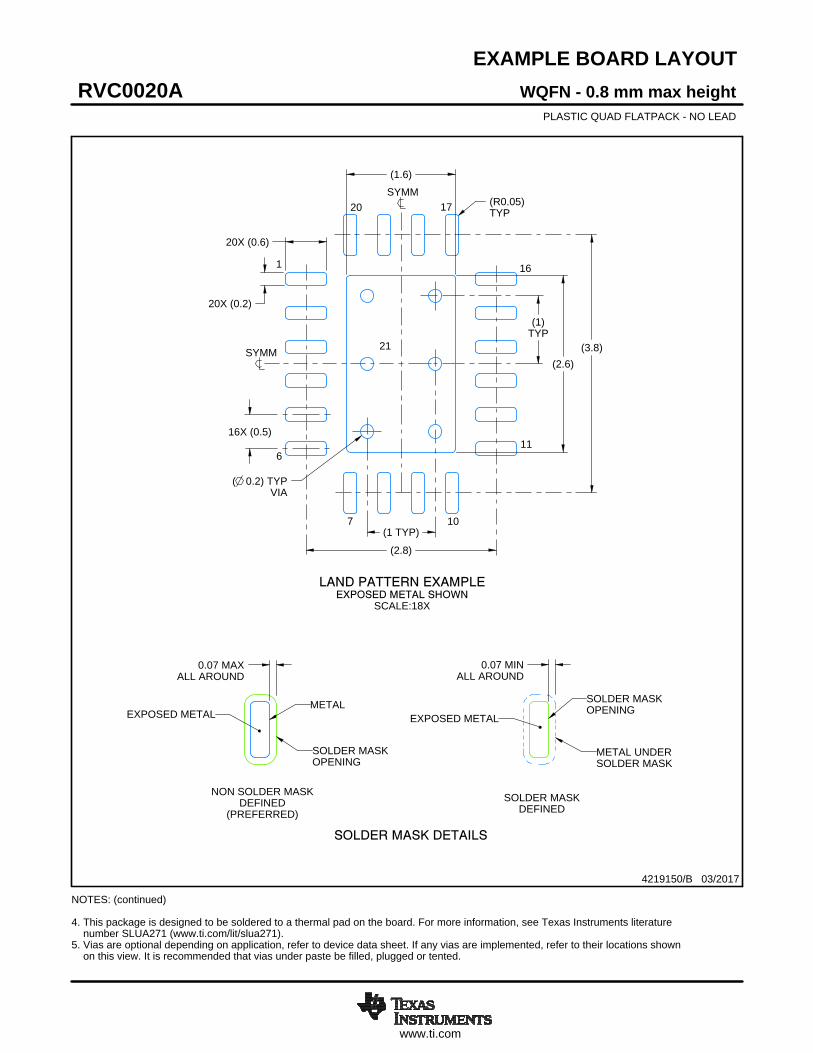
www.ti.com
EXAMPLE BOARD LAYOUT
0.07 MINALL AROUND
0.07 MAXALL AROUND
20X (0.2)
20X (0.6)
( 0.2) TYPVIA
16X (0.5)
(3.8)
(2.8)
(1)TYP
(1.6)
(R0.05)TYP
(2.6)
(1 TYP)
WQFN - 0.8 mm max heightRVC0020APLASTIC QUAD FLATPACK - NO LEAD
4219150/B 03/2017
SYMM
1
6
7 10
11
16
1720
SYMM
LAND PATTERN EXAMPLEEXPOSED METAL SHOWN
SCALE:18X
21
NOTES: (continued) 4. This package is designed to be soldered to a thermal pad on the board. For more information, see Texas Instruments literature number SLUA271 (www.ti.com/lit/slua271).5. Vias are optional depending on application, refer to device data sheet. If any vias are implemented, refer to their locations shown on this view. It is recommended that vias under paste be filled, plugged or tented.
SOLDER MASKOPENING
METAL UNDERSOLDER MASK
SOLDER MASKDEFINED
EXPOSED METALMETAL
SOLDER MASKOPENING
SOLDER MASK DETAILS
NON SOLDER MASKDEFINED
(PREFERRED)
EXPOSED METAL
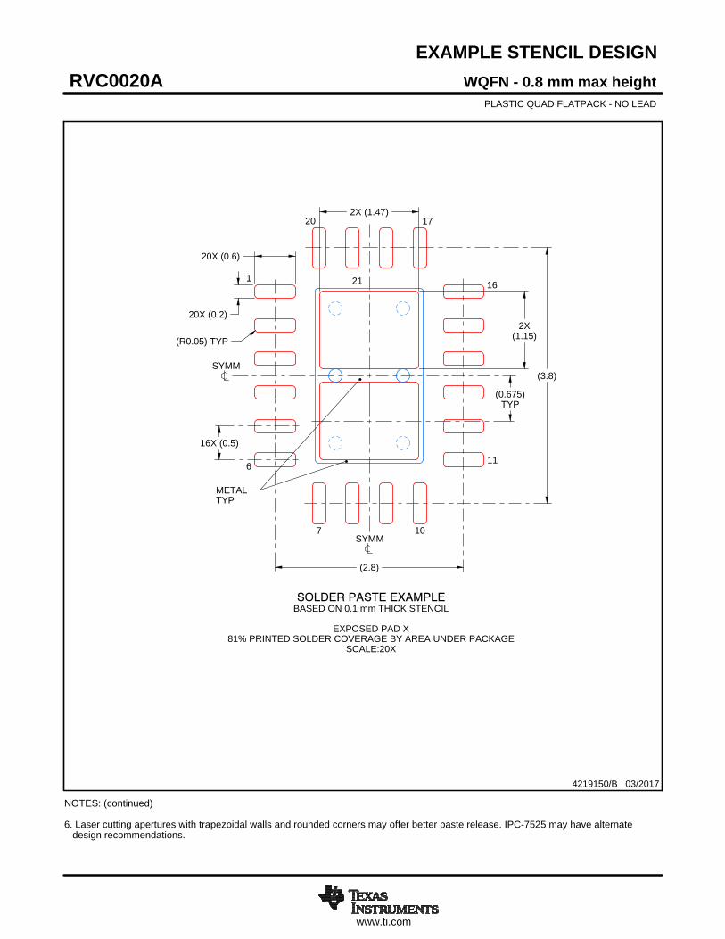
www.ti.com
EXAMPLE STENCIL DESIGN
20X (0.6)
20X (0.2)
16X (0.5)
(2.8)
(3.8)
2X (1.47)
(0.675)TYP
(R0.05) TYP2X
(1.15)
WQFN - 0.8 mm max heightRVC0020APLASTIC QUAD FLATPACK - NO LEAD
4219150/B 03/2017
NOTES: (continued) 6. Laser cutting apertures with trapezoidal walls and rounded corners may offer better paste release. IPC-7525 may have alternate design recommendations.
SYMM
METALTYP
SOLDER PASTE EXAMPLEBASED ON 0.1 mm THICK STENCIL
EXPOSED PAD X
81% PRINTED SOLDER COVERAGE BY AREA UNDER PACKAGESCALE:20X
SYMM
1
6
7 10
11
16
1720
21
IMPORTANT NOTICE
Texas Instruments Incorporated (TI) reserves the right to make corrections, enhancements, improvements and other changes to itssemiconductor products and services per JESD46, latest issue, and to discontinue any product or service per JESD48, latest issue. Buyersshould obtain the latest relevant information before placing orders and should verify that such information is current and complete.TI’s published terms of sale for semiconductor products (http://www.ti.com/sc/docs/stdterms.htm) apply to the sale of packaged integratedcircuit products that TI has qualified and released to market. Additional terms may apply to the use or sale of other types of TI products andservices.Reproduction of significant portions of TI information in TI data sheets is permissible only if reproduction is without alteration and isaccompanied by all associated warranties, conditions, limitations, and notices. TI is not responsible or liable for such reproduceddocumentation. Information of third parties may be subject to additional restrictions. Resale of TI products or services with statementsdifferent from or beyond the parameters stated by TI for that product or service voids all express and any implied warranties for theassociated TI product or service and is an unfair and deceptive business practice. TI is not responsible or liable for any such statements.Buyers and others who are developing systems that incorporate TI products (collectively, “Designers”) understand and agree that Designersremain responsible for using their independent analysis, evaluation and judgment in designing their applications and that Designers havefull and exclusive responsibility to assure the safety of Designers' applications and compliance of their applications (and of all TI productsused in or for Designers’ applications) with all applicable regulations, laws and other applicable requirements. Designer represents that, withrespect to their applications, Designer has all the necessary expertise to create and implement safeguards that (1) anticipate dangerousconsequences of failures, (2) monitor failures and their consequences, and (3) lessen the likelihood of failures that might cause harm andtake appropriate actions. Designer agrees that prior to using or distributing any applications that include TI products, Designer willthoroughly test such applications and the functionality of such TI products as used in such applications.TI’s provision of technical, application or other design advice, quality characterization, reliability data or other services or information,including, but not limited to, reference designs and materials relating to evaluation modules, (collectively, “TI Resources”) are intended toassist designers who are developing applications that incorporate TI products; by downloading, accessing or using TI Resources in anyway, Designer (individually or, if Designer is acting on behalf of a company, Designer’s company) agrees to use any particular TI Resourcesolely for this purpose and subject to the terms of this Notice.TI’s provision of TI Resources does not expand or otherwise alter TI’s applicable published warranties or warranty disclaimers for TIproducts, and no additional obligations or liabilities arise from TI providing such TI Resources. TI reserves the right to make corrections,enhancements, improvements and other changes to its TI Resources. TI has not conducted any testing other than that specificallydescribed in the published documentation for a particular TI Resource.Designer is authorized to use, copy and modify any individual TI Resource only in connection with the development of applications thatinclude the TI product(s) identified in such TI Resource. NO OTHER LICENSE, EXPRESS OR IMPLIED, BY ESTOPPEL OR OTHERWISETO ANY OTHER TI INTELLECTUAL PROPERTY RIGHT, AND NO LICENSE TO ANY TECHNOLOGY OR INTELLECTUAL PROPERTYRIGHT OF TI OR ANY THIRD PARTY IS GRANTED HEREIN, including but not limited to any patent right, copyright, mask work right, orother intellectual property right relating to any combination, machine, or process in which TI products or services are used. Informationregarding or referencing third-party products or services does not constitute a license to use such products or services, or a warranty orendorsement thereof. Use of TI Resources may require a license from a third party under the patents or other intellectual property of thethird party, or a license from TI under the patents or other intellectual property of TI.TI RESOURCES ARE PROVIDED “AS IS” AND WITH ALL FAULTS. TI DISCLAIMS ALL OTHER WARRANTIES ORREPRESENTATIONS, EXPRESS OR IMPLIED, REGARDING RESOURCES OR USE THEREOF, INCLUDING BUT NOT LIMITED TOACCURACY OR COMPLETENESS, TITLE, ANY EPIDEMIC FAILURE WARRANTY AND ANY IMPLIED WARRANTIES OFMERCHANTABILITY, FITNESS FOR A PARTICULAR PURPOSE, AND NON-INFRINGEMENT OF ANY THIRD PARTY INTELLECTUALPROPERTY RIGHTS. TI SHALL NOT BE LIABLE FOR AND SHALL NOT DEFEND OR INDEMNIFY DESIGNER AGAINST ANY CLAIM,INCLUDING BUT NOT LIMITED TO ANY INFRINGEMENT CLAIM THAT RELATES TO OR IS BASED ON ANY COMBINATION OFPRODUCTS EVEN IF DESCRIBED IN TI RESOURCES OR OTHERWISE. IN NO EVENT SHALL TI BE LIABLE FOR ANY ACTUAL,DIRECT, SPECIAL, COLLATERAL, INDIRECT, PUNITIVE, INCIDENTAL, CONSEQUENTIAL OR EXEMPLARY DAMAGES INCONNECTION WITH OR ARISING OUT OF TI RESOURCES OR USE THEREOF, AND REGARDLESS OF WHETHER TI HAS BEENADVISED OF THE POSSIBILITY OF SUCH DAMAGES.Unless TI has explicitly designated an individual product as meeting the requirements of a particular industry standard (e.g., ISO/TS 16949and ISO 26262), TI is not responsible for any failure to meet such industry standard requirements.Where TI specifically promotes products as facilitating functional safety or as compliant with industry functional safety standards, suchproducts are intended to help enable customers to design and create their own applications that meet applicable functional safety standardsand requirements. Using products in an application does not by itself establish any safety features in the application. Designers mustensure compliance with safety-related requirements and standards applicable to their applications. Designer may not use any TI products inlife-critical medical equipment unless authorized officers of the parties have executed a special contract specifically governing such use.Life-critical medical equipment is medical equipment where failure of such equipment would cause serious bodily injury or death (e.g., lifesupport, pacemakers, defibrillators, heart pumps, neurostimulators, and implantables). Such equipment includes, without limitation, allmedical devices identified by the U.S. Food and Drug Administration as Class III devices and equivalent classifications outside the U.S.TI may expressly designate certain products as completing a particular qualification (e.g., Q100, Military Grade, or Enhanced Product).Designers agree that it has the necessary expertise to select the product with the appropriate qualification designation for their applicationsand that proper product selection is at Designers’ own risk. Designers are solely responsible for compliance with all legal and regulatoryrequirements in connection with such selection.Designer will fully indemnify TI and its representatives against any damages, costs, losses, and/or liabilities arising out of Designer’s non-compliance with the terms and provisions of this Notice.
Mailing Address: Texas Instruments, Post Office Box 655303, Dallas, Texas 75265Copyright © 2018, Texas Instruments Incorporated


![[PPT]Rigging, Signals, Power Line Safety & Assembly ...lni.wa.gov/Safety/Topics/AtoZ/Cranes/files/Construction... · Web viewTitle Rigging, Signals, Power Line Safety & Assembly](https://img.pdfslide.us/doc/110x75/5af7d12a7f8b9aac248c4b9e/pptrigging-signals-power-line-safety-assembly-lniwagovsafetytopicsatozcranesfilesconstructionweb.jpg)