Embed Size (px)
Citation preview
TUSB9260USB 3.0 TO SATA BRIDGE
Data Manual
PRODUCTION DATA information is current as of publication date.Products conform to specifications per the terms of the TexasInstruments standard warranty. Production processing does notnecessarily include testing of all parameters.
Literature Number: SLLS962D
December 2009–Revised May 2011
TUSB9260
SLLS962D–DECEMBER 2009–REVISED MAY 2011 www.ti.com
Contents1 MAIN FEATURES ................................................................................................................ 5
1.1 TUSB9260 Features ........................................................................................................ 5
1.2 Target Applications ......................................................................................................... 52 INTRODUCTION .................................................................................................................. 6
2.1 System Overview ........................................................................................................... 6
2.2 Device Block Diagram ...................................................................................................... 63 OPERATION ....................................................................................................................... 8
3.1 General Functionality ....................................................................................................... 8
3.2 Firmware Support ........................................................................................................... 9
3.3 GPIO/PWM LED Designations ............................................................................................ 9
3.4 Power Up and Reset Sequence ......................................................................................... 10
4 SIGNAL DESCRIPTIONS ..................................................................................................... 115 CLOCK CONNECTIONS ...................................................................................................... 15
5.1 Clock Source Requirements ............................................................................................. 15
5.2 Clock Source Selection Guide ........................................................................................... 15
5.3 Oscillator .................................................................................................................... 16
5.4 Crystal ....................................................................................................................... 166 ELECTRICAL SPECIFICATIONS .......................................................................................... 17
6.1 Absolute Maximum Ratings .............................................................................................. 17
6.2 Recommended Operating Conditions .................................................................................. 17
6.3 DC Electrical Characteristics for 3.3-V Digital I/O ..................................................................... 177 POWER CONSUMPTION ..................................................................................................... 18
2 Contents Copyright © 2009–2011, Texas Instruments Incorporated
TUSB9260
www.ti.com SLLS962D–DECEMBER 2009–REVISED MAY 2011
List of Figures2-1 Device Block Diagram............................................................................................................. 7
5-1 Typical Crystal Connections .................................................................................................... 15
Copyright © 2009–2011, Texas Instruments Incorporated List of Figures 3
TUSB9260
SLLS962D–DECEMBER 2009–REVISED MAY 2011 www.ti.com
List of Tables3-1 GPIO/PWM LED Designations................................................................................................... 9
4-1 I/O Definitions..................................................................................................................... 11
4-2 Clock and Reset Signals ........................................................................................................ 11
4-3 SATA Interface Signals.......................................................................................................... 11
4-4 USB Interface Signals ........................................................................................................... 12
4-5 Serial Peripheral Interface (SPI) Signals ...................................................................................... 12
4-6 JTAG, GPIO, and PWM Signals ............................................................................................... 13
4-7 Power and Ground Signals ..................................................................................................... 14
5-1 Oscillator Specification .......................................................................................................... 16
5-2 Crystal Specification ............................................................................................................. 16
7-1 SuperSpeed USB Power Consumption ....................................................................................... 18
7-2 High Speed USB Power Consumption ........................................................................................ 18
4 List of Tables Copyright © 2009–2011, Texas Instruments Incorporated
TUSB9260
www.ti.com SLLS962D–DECEMBER 2009–REVISED MAY 2011
USB 3.0 TO SATA BRIDGECheck for Samples: TUSB9260
1 MAIN FEATURES
1.1 TUSB9260 Features1• Universal Serial Bus (USB)
– SuperSpeed USB 3.0 Compliant - TID 340000007• Integrated Transceiver Supports SS/HS/FS Signaling
– Best in Class Adaptive Equalizer• Allows for Greater Jitter Tolerance in the Receiver
– USB Class Support• USB Attached SCSI Protocol (UASP)• USB Mass Storage Class Bulk-Only Transport (BOT)• Support for Error Conditions Per the 13 Cases (Defined in the BOT Specification)• USB Bootability Support• USB Human Interface Device (HID)
– Supports Firmware Update Via USB, Using a TI Provided Application• SATA Interface
– Serial ATA Specification Revision 2.6• gen1i, gen1m, gen2i, and gen2m
– Support for Mass-Storage Devices Compatible With the ATA/ATAPI-8 Specification• Integrated ARM Cortex M3 Core
– Customizable Application Code Loaded From EEPROM Via SPI Interface– Two Additional SPI Port Chip Selects for Peripheral Connection– Up to 12 GPIOs for End-User Configuration
• 2 GPIOs Have PWM Functionality for LED Blink Speed Control– Serial Communications Interface for Debug (UART)
• General Features– Can Operate from Either a Single Low Cost Crystal or Clock Oscillator
• Supports 40 MHz– A JTAG Interface is Used for IEEE1149.1 and IEEE1149.6 Boundary Scan– Available in a Fully RoHS Compliant Package
1.2 Target Applications• External HDD/SSD• External DVD• External CD• HDD-Based Portable Media Player
1
Please be aware that an important notice concerning availability, standard warranty, and use in critical applications of TexasInstruments semiconductor products and disclaimers thereto appears at the end of this data sheet.
PRODUCTION DATA information is current as of publication date. Copyright © 2009–2011, Texas Instruments IncorporatedProducts conform to specifications per the terms of the TexasInstruments standard warranty. Production processing does notnecessarily include testing of all parameters.

SATAGen1/2
TUSB9260
HDD
USB 3.0SuperSpeed
(1)
USB 2.0High-speed
(1)
PCwith
USB 3.0Support
(1) USB connection is made at either SuperSpeed or High-Speed depending on the upstream connection support.
TUSB9260
SLLS962D–DECEMBER 2009–REVISED MAY 2011 www.ti.com
2 INTRODUCTION
2.1 System Overview
The TUSB9260 is an ARM cortex M3 microcontroller based USB 3.0 to serial ATA bridge. It provides thenecessary hardware and firmware to implement a USB attached SCSI protocol (UASP) compliant massstorage device suitable for bridging hard disk drives (HDD), solid state disk drives (SSD), optical drivesand other compatible SATA 1.5-Gbps or SATA 3.0-Gbps devices to a USB 3.0 bus. In addition to UASPsupport, the firmware implements the mass storage class bulk-only transport (BOT), and USB humanin-terface device (HID) interfaces.
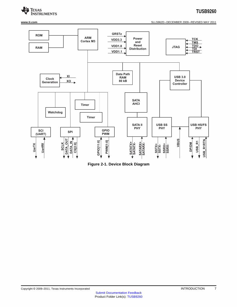
2.2 Device Block Diagram
The major functional blocks are as follows:• Cortex M3 microcontroller subsystem including the following peripherals:
– Time interrupt modules, including watchdog timer– Universal asynchronous receive/transmit (SCI)– Serial peripheral interface (SPI)– General purpose input/output (GPIO)– PWM for support of PWM outputs (PWM)
• USB 3.0 core (endpoint controller) and integrated SuperSpeed PHY• AHCI compliant SATA controller and integrated SATA PHY
– Supporting gen1i, gen1m, gen2i, and gen2m• Chip level clock generation and distribution• Support for JTAG 1149.1 and 1149.6
6 INTRODUCTION Copyright © 2009–2011, Texas Instruments Incorporated
Submit Documentation FeedbackProduct Folder Link(s): TUSB9260
ROM
RAM
ARMCortex M3
Powerand
ResetDistribution
JTAG
ClockGeneration
TCKTMSTDOTDITRST
XI
XO
SCI(UART)
Watchdog
SPI
Timer
GPIOPWM
Ua
rtR
X
Ua
rTX
SC
LK
Timer
Data PathRAM80 kB
SA
TA
TX
+S
ATA
TX
-
SA
TA
RX
+S
ATA
RX
-
SATA IIPHY
USB SSPHY
USB HS/FSPHY
SATAAHCI
USB 3.0Device
Controller
SS
TX
+S
ST
X-
SS
RX
+S
SR
X-
VB
US
VDD3.3
VDD1.8
VDD1.1
DA
TA
_O
UT
DA
TA
_IN
CS
[2:0
]
GP
IO[1
1:0
]
PW
M[1
:0]
DP
/DM
US
B_
R1
US
B_
R1
RT
N
GRSTz
TUSB9260
www.ti.com SLLS962D–DECEMBER 2009–REVISED MAY 2011
Figure 2-1. Device Block Diagram
Copyright © 2009–2011, Texas Instruments Incorporated INTRODUCTION 7Submit Documentation FeedbackProduct Folder Link(s): TUSB9260
TUSB9260
SLLS962D–DECEMBER 2009–REVISED MAY 2011 www.ti.com
3 OPERATION
3.1 General Functionality
The TUSB9260 ROM contains boot code that executes after a global reset which performs the initialcon-figuration required to load a firmware image from an attached SPI flash memory to local RAM. In theab-sence of an attached SPI flash memory or a valid image in the SPI flash memory, the firmware will idleand wait for a connection from a USB host through its HID interface which is also configured from the bootcode. The latter can be accomplished using a custom application or driver to load the firmware from a fileresident on the host system.
Once the firmware is loaded it configures the SATA advanced host controller interface host bus adapter(AHCI) and the USB device controller. In addition, the configuration of the AHCI includes a port resetwhich initiates an out of band (OOB) TX sequence from the AHCI link layer to determine if a device isconnected, and if so negotiate the connection speed with the device (3.0 Gbps or 1.5 Gbps).
The configuration of the USB device controller includes creation of the descriptors and configuration of thedevice endpoints for support of UASP and USB mass storage class bulk-only transport (BOT). In addition,the firmware provides any other custom configuration required for application specific implementation, forexample a HID interface for user initiated backup.
After USB device controller configuration is complete, if a SATA device was detected during the AHCIcon-figuration the firmware connects the device to the USB bus when VBUS is detected. According to theUSB 3.0 specification, the TUSB9260 will initially try to connect at SuperSpeed, if successful it will enterU0; otherwise, after the training time out it will enable the DP pull up and connect as a USB 2.0high-speed or full-speed device depending on the speed supported by host or hub port.
When connected, the firmware presents the BOT interface as the primary interface and the UASPinter-face as the secondary interface. If the host stack is UASP aware, it can enable the UASP interfaceusing a SET_INTERFACE request for alternate interface 1.
Following speed negotiation, the device should transmit a device to host (D2H) FIS with the devicesignature. This first D2H FIS is received by the link layer and copied to the port signature register. Whenfirmware is notified of the device connection it queries the device for capabilities using the IDENTIFYDEVICE command. Firmware then configures the device as appropriate for its interface and featuressupported, for example an HDD that supports native command queuing (NCQ).
The configuration of the USB device controller includes creation of the descriptors, configuration of thedevice endpoints for support of UASP and USB mass storage class bulk-only transport (BOT), allocationof memory for the transmit request blocks (TRBs), and creation of the TRBs necessary to transmit andreceive packet data over the USB. In addition, the firmware provides any other custom configurationrequired for application specific implementation, for example a HID interface for user initiated backup.
After USB device controller configuration is complete, if a SATA device was detected during the AHCIconfiguration the firmware connects the device to the USB bus when VBUS is detected. According to theUSB 3.0 specification, the TUSB9260 will initially try to connect at SuperSpeed, if successful it will enterU0; otherwise, after the training time out it will enable the DP pull up and connect as a USB 2.0high-speed or full-speed device depending on the speed supported by host or hub port.
When connected as a SuperSpeed device, the firmware presents the UASP interface as the primaryinterface, and the BOT interface as a secondary interface. If the host stack is not UASP aware, it canenable the BOT interface using a SET_INTERFACE request for alternate interface 1.
8 OPERATION Copyright © 2009–2011, Texas Instruments Incorporated
Submit Documentation FeedbackProduct Folder Link(s): TUSB9260
TUSB9260
www.ti.com SLLS962D–DECEMBER 2009–REVISED MAY 2011
3.2 Firmware Support
Default firmware support is provided for the following:• USB 3.0 SuperSpeed and USB 2.0 High-Speed and Full-Speed• USB Attached SCSI Protocol (UASP)• USB Mass Storage Class (MSC) Bulk-Only Transport (BOT)
– Including the 13 Error Cases• USB Mass Storage Specification for Bootability• USB Device Class Definition for Human Interface Devices (HID)
– Firmware Update and Custom Functionality (e.g. One-Touch Backup)• Serial ATA Advanced Host Controller Interface (AHCI)• General Purpose Input/Output (GPIO)
– LED Control and Custom Functions (e.g. One-Touch Backup Control)• Pulse Width Modulation (PWM)
– LED Dimming Control• Serial Peripheral Interface (SPI)
– Firmware storage and storing Custom Device Descriptors• Serial Communications Interface (SCI)
– Debug Output Only
3.3 GPIO/PWM LED Designations
The default firmware provided by TI drives the GPIO and PWM outputs as listed in the table below.
Table 3-1. GPIO/PWM LED Designations
GPIO0 SW heartbeat
00: U3 state or default
01: U2 stateGPIO1/GPIO5 USB3 power state (U0-U3)
10: U1 state
11: U0 state
GPIO2 HS/FS suspend
GPIO3 Push button input on customer board
GPIO4 Not used
GPIO6 FS/HS connected
GPIO7 SS connected
PWM0 Disk activity
PWM1 U3 or HS/FS suspend state (fades high and low)
GPIO10 Not used(SPICS1)
GPIO11 Not used(SPICS2)
The LED’s on the TUSB9260 Product Development Kit (PDK) board are connected as in the table above.Please see the TUSB9260 PDK Guide (SLLA303) for more information on GPIO LED connection andusage. This EVM is available for purchase, contact TI for ordering information.
Copyright © 2009–2011, Texas Instruments Incorporated OPERATION 9Submit Documentation FeedbackProduct Folder Link(s): TUSB9260
TUSB9260
SLLS962D–DECEMBER 2009–REVISED MAY 2011 www.ti.com
3.4 Power Up and Reset Sequence
The TUSB9260 does not have specific power sequencing requirements with respect to the core power(VDD), I/O power (VDD33), or analog power (VDDA11, VDDA33, VDDA18, and VDDR18). The corepower (VDD) or IO power (VDD33) may be powered up for an indefinite period of time while others are notpowered up if all of these constraints are met:• All maximum ratings and recommended operating conditions are observed.• All warnings about exposure to maximum rated and recommended conditions are observed,
par-ticularly junction temperature. These apply to power transitions as well as normal operation.• Bus contention while VDD33 is powered up must be limited to 100 hours over the projected life-time of
the device.• Bus contention while VDD33 is powered down may violate the absolute maximum ratings.
A supply bus is powered up when the voltage is within the recommended operating range. It is powereddown when it is below that range, either stable or in transition.
A minimum reset duration of 1 ms is required. This is defined as the time when the power supplies are inthe recommended operating range to the de-assertion of GRSTz.
10 OPERATION Copyright © 2009–2011, Texas Instruments Incorporated
Submit Documentation FeedbackProduct Folder Link(s): TUSB9260
TUSB9260
www.ti.com SLLS962D–DECEMBER 2009–REVISED MAY 2011
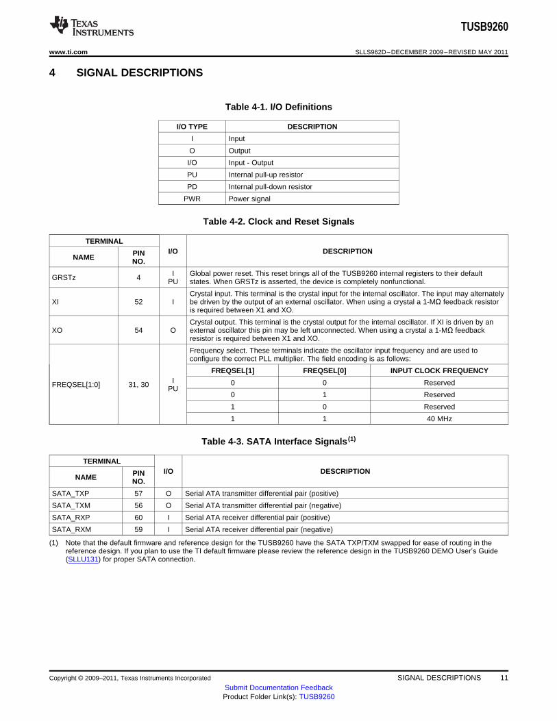
4 SIGNAL DESCRIPTIONS
Table 4-1. I/O Definitions
I/O TYPE DESCRIPTION
I Input
O Output
I/O Input - Output
PU Internal pull-up resistor
PD Internal pull-down resistor
PWR Power signal
Table 4-2. Clock and Reset Signals
TERMINALI/O DESCRIPTIONPINNAME NO.
I Global power reset. This reset brings all of the TUSB9260 internal registers to their defaultGRSTz 4 PU states. When GRSTz is asserted, the device is completely nonfunctional.
Crystal input. This terminal is the crystal input for the internal oscillator. The input may alternatelyXI 52 I be driven by the output of an external oscillator. When using a crystal a 1-MΩ feedback resistor
is required between X1 and XO.
Crystal output. This terminal is the crystal output for the internal oscillator. If XI is driven by anXO 54 O external oscillator this pin may be left unconnected. When using a crystal a 1-MΩ feedback
resistor is required between X1 and XO.
Frequency select. These terminals indicate the oscillator input frequency and are used toconfigure the correct PLL multiplier. The field encoding is as follows:
FREQSEL[1] FREQSEL[0] INPUT CLOCK FREQUENCYI 0 0 ReservedFREQSEL[1:0] 31, 30 PU
0 1 Reserved
1 0 Reserved
1 1 40 MHz
Table 4-3. SATA Interface Signals (1)
TERMINALI/O DESCRIPTIONPINNAME NO.
SATA_TXP 57 O Serial ATA transmitter differential pair (positive)
SATA_TXM 56 O Serial ATA transmitter differential pair (negative)
SATA_RXP 60 I Serial ATA receiver differential pair (positive)
SATA_RXM 59 I Serial ATA receiver differential pair (negative)
(1) Note that the default firmware and reference design for the TUSB9260 have the SATA TXP/TXM swapped for ease of routing in thereference design. If you plan to use the TI default firmware please review the reference design in the TUSB9260 DEMO User’s Guide(SLLU131) for proper SATA connection.
Copyright © 2009–2011, Texas Instruments Incorporated SIGNAL DESCRIPTIONS 11Submit Documentation FeedbackProduct Folder Link(s): TUSB9260
TUSB9260
SLLS962D–DECEMBER 2009–REVISED MAY 2011 www.ti.com
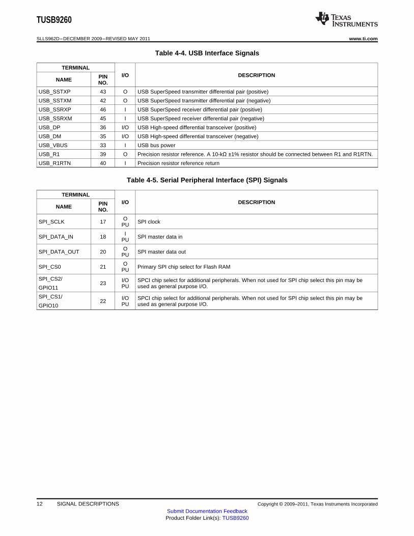
Table 4-4. USB Interface Signals
TERMINALI/O DESCRIPTIONPINNAME NO.
USB_SSTXP 43 O USB SuperSpeed transmitter differential pair (positive)
USB_SSTXM 42 O USB SuperSpeed transmitter differential pair (negative)
USB_SSRXP 46 I USB SuperSpeed receiver differential pair (positive)
USB_SSRXM 45 I USB SuperSpeed receiver differential pair (negative)
USB_DP 36 I/O USB High-speed differential transceiver (positive)
USB_DM 35 I/O USB High-speed differential transceiver (negative)
USB_VBUS 33 I USB bus power
USB_R1 39 O Precision resistor reference. A 10-kΩ ±1% resistor should be connected between R1 and R1RTN.
USB_R1RTN 40 I Precision resistor reference return
Table 4-5. Serial Peripheral Interface (SPI) Signals
TERMINALI/O DESCRIPTIONPINNAME NO.
OSPI_SCLK 17 SPI clockPU
ISPI_DATA_IN 18 SPI master data inPU
OSPI_DATA_OUT 20 SPI master data outPU
OSPI_CS0 21 Primary SPI chip select for Flash RAMPU
SPI_CS2/ I/O SPCI chip select for additional peripherals. When not used for SPI chip select this pin may be23 PU used as general purpose I/O.GPIO11
SPI_CS1/ I/O SPCI chip select for additional peripherals. When not used for SPI chip select this pin may be22 PU used as general purpose I/O.GPIO10
12 SIGNAL DESCRIPTIONS Copyright © 2009–2011, Texas Instruments Incorporated
Submit Documentation FeedbackProduct Folder Link(s): TUSB9260

TUSB9260
www.ti.com SLLS962D–DECEMBER 2009–REVISED MAY 2011
Table 4-6. JTAG, GPIO, and PWM Signals
TERMINALI/O DESCRIPTIONPINNAME NO.
IJTAG_TCK 25 JTAG test clockPD
IJTAG_TDI 26 JTAG test data inPU
OJTAG_TDO 27 JTAG test data outPD
IJTAG_TMS 28 JTAG test mode selectPU
IJTAG_TRSTz 29 JTAG test resetPD
I/O GPIO/UART transmitter. This terminal can be configured as a GPIO or as the transmitter for aGPIO9/UART_TX 6 PU UART channel. This pin defaults to a general purpose output.
I/O GPIO/UART receiver. This terminal can be configured as a GPIO or as the receiver for a UARTGPIO8/UART_RX 5 PU channel. This pin defaults to a general purpose output.
I/OGPIO7 16 PD
I/OGPIO6 15 PD
I/OGPIO5 14 PD
I/OGPIO4 13 PDConfigurable as general purpose input/outputs
I/OGPIO3 11 PD
I/OGPIO2 10 PD
I/OGPIO1 9 PD
I/OGPIO0 8 PD
OPWM0 2 PD (1)
Pulse Width Modulation (PWM). Can be used to drive status LED's.OPWM1 3 PD (1)
(1) PWM pull down resistors are disabled by default. A firmware modification is required to turn them on. All other internal pull up/downresistors are enabled by default.
Copyright © 2009–2011, Texas Instruments Incorporated SIGNAL DESCRIPTIONS 13Submit Documentation FeedbackProduct Folder Link(s): TUSB9260
TUSB9260
SLLS962D–DECEMBER 2009–REVISED MAY 2011 www.ti.com
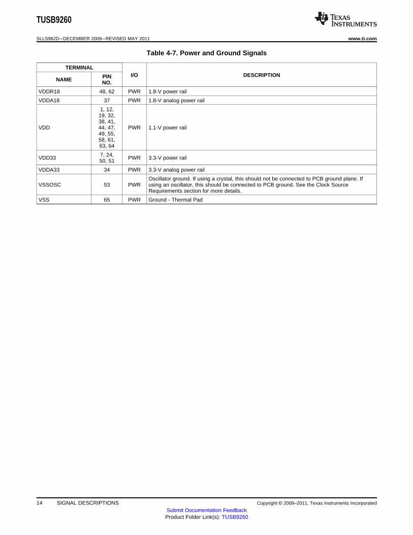
Table 4-7. Power and Ground Signals
TERMINALI/O DESCRIPTIONPINNAME NO.
VDDR18 48, 62 PWR 1.8-V power rail
VDDA18 37 PWR 1.8-V analog power rail
1, 12,19, 32,38, 41,
VDD 44, 47, PWR 1.1-V power rail49, 55,58, 61,63, 64
7, 24,VDD33 PWR 3.3-V power rail50, 51
VDDA33 34 PWR 3.3-V analog power rail
Oscillator ground. If using a crystal, this should not be connected to PCB ground plane. IfVSSOSC 53 PWR using an oscillator, this should be connected to PCB ground. See the Clock Source
Requirements section for more details.
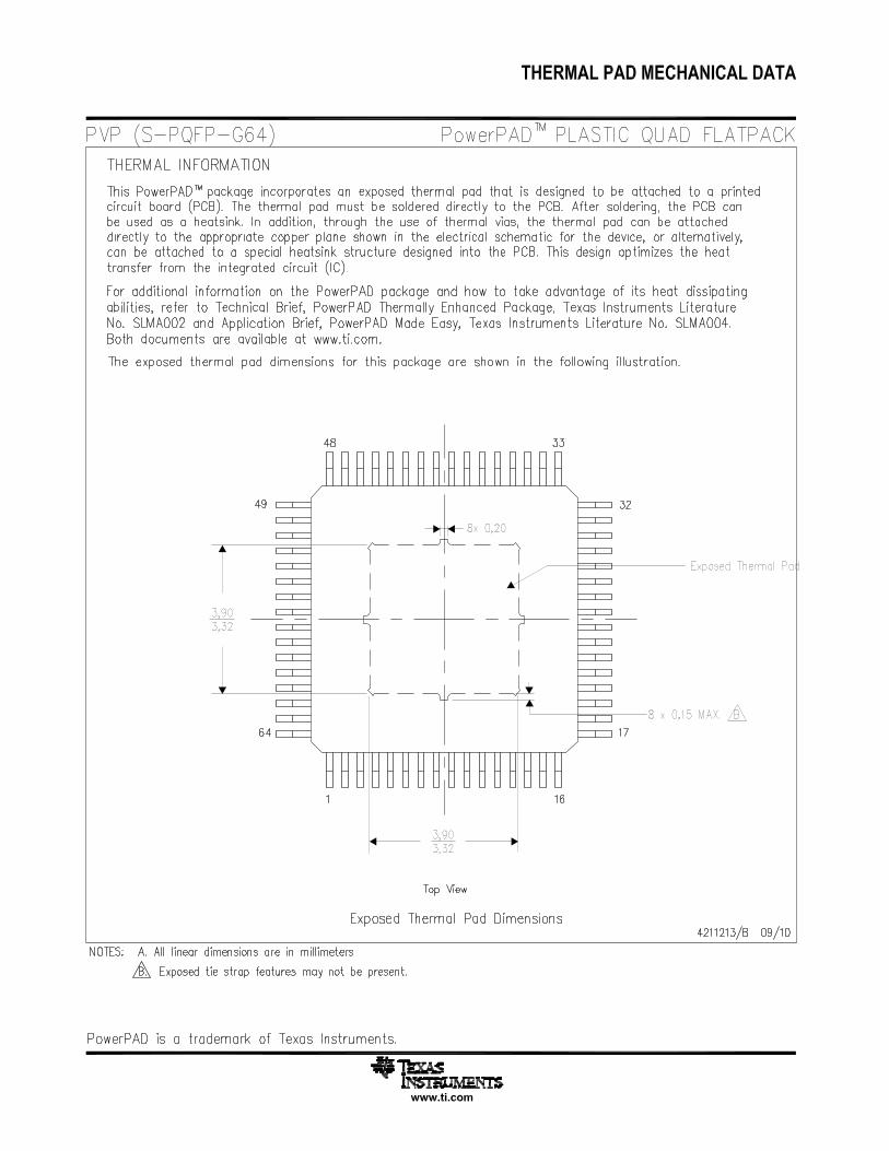
VSS 65 PWR Ground - Thermal Pad
14 SIGNAL DESCRIPTIONS Copyright © 2009–2011, Texas Instruments Incorporated
Submit Documentation FeedbackProduct Folder Link(s): TUSB9260
TUSB9260
www.ti.com SLLS962D–DECEMBER 2009–REVISED MAY 2011
5 CLOCK CONNECTIONS
5.1 Clock Source Requirements
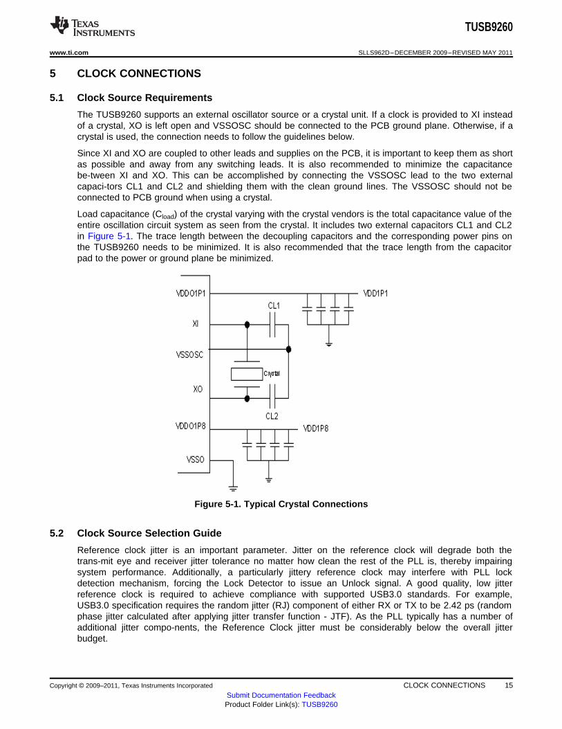
The TUSB9260 supports an external oscillator source or a crystal unit. If a clock is provided to XI insteadof a crystal, XO is left open and VSSOSC should be connected to the PCB ground plane. Otherwise, if acrystal is used, the connection needs to follow the guidelines below.
Since XI and XO are coupled to other leads and supplies on the PCB, it is important to keep them as shortas possible and away from any switching leads. It is also recommended to minimize the capacitancebe-tween XI and XO. This can be accomplished by connecting the VSSOSC lead to the two externalcapaci-tors CL1 and CL2 and shielding them with the clean ground lines. The VSSOSC should not beconnected to PCB ground when using a crystal.
Load capacitance (Cload) of the crystal varying with the crystal vendors is the total capacitance value of theentire oscillation circuit system as seen from the crystal. It includes two external capacitors CL1 and CL2in Figure 5-1. The trace length between the decoupling capacitors and the corresponding power pins onthe TUSB9260 needs to be minimized. It is also recommended that the trace length from the capacitorpad to the power or ground plane be minimized.
Figure 5-1. Typical Crystal Connections
5.2 Clock Source Selection Guide
Reference clock jitter is an important parameter. Jitter on the reference clock will degrade both thetrans-mit eye and receiver jitter tolerance no matter how clean the rest of the PLL is, thereby impairingsystem performance. Additionally, a particularly jittery reference clock may interfere with PLL lockdetection mechanism, forcing the Lock Detector to issue an Unlock signal. A good quality, low jitterreference clock is required to achieve compliance with supported USB3.0 standards. For example,USB3.0 specification requires the random jitter (RJ) component of either RX or TX to be 2.42 ps (randomphase jitter calculated after applying jitter transfer function - JTF). As the PLL typically has a number ofadditional jitter compo-nents, the Reference Clock jitter must be considerably below the overall jitterbudget.
Copyright © 2009–2011, Texas Instruments Incorporated CLOCK CONNECTIONS 15Submit Documentation FeedbackProduct Folder Link(s): TUSB9260

TUSB9260
SLLS962D–DECEMBER 2009–REVISED MAY 2011 www.ti.com
5.3 Oscillator
XI should be tied to the 1.8-V clock source and XO should be left floating.
VSSOSC should be connected to the PCB ground plane.
A 40-MHz clock can be used.
Table 5-1. Oscillator Specification
PARAMETER CONDITIONS MIN TYP MAX UNIT
VDDIO = 1.8 V,CXI XI input capacitance 0.414 pFTJ = 25°CVIL Low-level input voltage 0.35 x VDDR18 V
VIH High-level input voltage 0.65 x VDDR18 V
Ttosc_i Frequency tolerance Operational temperature –50 50 ppm
Tduty Duty cycle 45 50 55 %
TR/TF Rise/Fall time 20% - 80 % 6 ns
RJ Reference clock RJ JTF (1 sigma) (1) (2) 0.8 ps
TJ Reference clock TJ JTF (total p-p) (2) (3) 25 ps
Tp-p Reference clock jitter (absolute p-p) (4) 50 ps
(1) Sigma value assuming Gaussian distribution(2) After application of JTF(3) Calculated as 14.1 x RJ + DJ(4) Absolute phase jitter (p-p)
5.4 Crystal
A parallel, 20-pF load capacitor should be used if a crystal source is used.
VSSOSC should not be connected to the PCB ground plane.
A 40-MHz crystal can be used.
Table 5-2. Crystal Specification
PARAMETER CONDITIONS MIN TYP MAX UNIT
Ttosc_i Frequency tolerance Operational temperature –50 50 ppm
Frequency stability 1 year aging –50 50 ppm
CL Load capacitance 12 20 24 pF
16 CLOCK CONNECTIONS Copyright © 2009–2011, Texas Instruments Incorporated
Submit Documentation FeedbackProduct Folder Link(s): TUSB9260
TUSB9260
www.ti.com SLLS962D–DECEMBER 2009–REVISED MAY 2011
6 ELECTRICAL SPECIFICATIONS
6.1 Absolute Maximum Ratingsover operating free-air temperature range (unless otherwise noted)
VALUE UNIT
VDDR18/ Steady-state supply voltage –0.3 to 2.45 VVDDA18
VDD Steady-state supply voltage –0.3 to 1.4 V
VDD33/ Steady-state supply voltage –0.3 to 3.8 VVDDA33
6.2 Recommended Operating Conditionsover operating free-air temperature range (unless otherwise noted)
MIN NOM MAX UNIT
VDDR18 Digital 1.8 supply voltage 1.71 1.8 1.89 V
VDDA18 Analog 1.8 supply voltage 1.62 1.8 1.89 V
VDD Digital 1.1 supply voltage 1.045 1.1 1.155 V
VDD33 Digital 3.3 supply voltage 3 3.3 3.6 V
VDDA33 Analog 3.3 supply voltage 3 3.3 3.6 V
VBUS Voltage at VBUS PAD 0 1.155 V
TA Operating free-air temperature range 0 70 °CTJ Operating junction temperature range 0 105 °C
HBM ESD 1000 V
CDM ESD 500 V
6.3 DC Electrical Characteristics for 3.3-V Digital I/Oover operating free-air temperature range (unless otherwise noted)
PARAMETER TEST CONDITIONS MIN TYP MAX UNIT
DRIVER
TR Rise time 5 pF 1.5 ns
TF Fall time 5 pF 1.53 ns
IOL Low-level output current VDD33 = 3.3 V, TJ = 25°C 6 mA
IOH High-level output current VDD33 = 3.3 V, TJ = 25°C –6 mA
VOL Low-level output voltage IOL = 2 mA 0.4 V
VOH High-level output voltage IOL = –2 mA 2.4 V
VO Output voltage 0 VDD33 V
RECEIVER
VI Input voltage 0 VDD33 V
VIL Low-level input voltage 0 0.8 V
VIH High-level input voltage 2 V
Vhys Input hysteresis 200 mV
tT Input transition time (TR and TF) 10 ns
II Input current VI = 0 V to VDD33 12 µA
CI Input capacitance VDD33 = 3.3 V, TJ = 25°C 0.384 pF
Copyright © 2009–2011, Texas Instruments Incorporated ELECTRICAL SPECIFICATIONS 17Submit Documentation FeedbackProduct Folder Link(s): TUSB9260

TUSB9260
SLLS962D–DECEMBER 2009–REVISED MAY 2011 www.ti.com
7 POWER CONSUMPTION
All transfers are to a SATA Gen II SSD. A SATA Gen I target yields an approximate 10-mA power savingson the 1.1-V rail.
Table 7-1. SuperSpeed USB Power Consumption
TYPICAL IDLE CURRENTPOWER RAIL TYPICAL ACTIVE CURRENT (mA) (1)(mA) (2)
VDD11 (3) 319 308
VDD18 (4) 58 58
VDD33 (5) 6 6
(1) Transferring data via SS USB to a SSD SATA Gen II device. No SATA power management, U0 only.(2) SATA Gen II SSD attached no active transfer. No SATA power management, U0 only.(3) All 1.1-V power rails connected together.(4) All 1.8-V power rails connected together.(5) All 3.3-V power rails connected together.
Table 7-2. High Speed USB Power Consumption
TYPICAL IDLE CURRENTPOWER RAIL TYPICAL ACTIVE CURRENT (mA) (1)(mA) (2)
VDD11 (3) 197 193
VDD18 (4) 45 36
VDD33 (5) 14 14
(1) Transferring data via HS USB to a SSD SATA Gen II device. No SATA power management.(2) SATA Gen II SSD attached no active transfer. No SATA power management.(3) All 1.1-V power rails connected together.(4) All 1.8-V power rails connected together.(5) All 3.3-V power rails connected together.
18 POWER CONSUMPTION Copyright © 2009–2011, Texas Instruments Incorporated
Submit Documentation FeedbackProduct Folder Link(s): TUSB9260

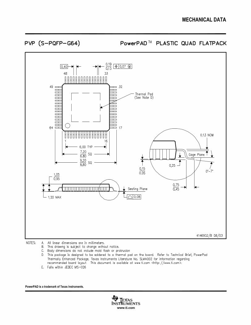
PACKAGE OPTION ADDENDUM
www.ti.com 18-May-2018
Addendum-Page 1
PACKAGING INFORMATION
Orderable Device Status(1)
Package Type PackageDrawing
Pins PackageQty
Eco Plan(2)
Lead/Ball Finish(6)
MSL Peak Temp(3)
Op Temp (°C) Device Marking(4/5)
Samples
TUSB9260PVP NRND HTQFP PVP 64 250 Green (RoHS& no Sb/Br)
CU NIPDAU Level-3-260C-168 HR 0 to 70 TUSB9260
(1) The marketing status values are defined as follows:ACTIVE: Product device recommended for new designs.LIFEBUY: TI has announced that the device will be discontinued, and a lifetime-buy period is in effect.NRND: Not recommended for new designs. Device is in production to support existing customers, but TI does not recommend using this part in a new design.PREVIEW: Device has been announced but is not in production. Samples may or may not be available.OBSOLETE: TI has discontinued the production of the device.
(2) RoHS: TI defines "RoHS" to mean semiconductor products that are compliant with the current EU RoHS requirements for all 10 RoHS substances, including the requirement that RoHS substancedo not exceed 0.1% by weight in homogeneous materials. Where designed to be soldered at high temperatures, "RoHS" products are suitable for use in specified lead-free processes. TI mayreference these types of products as "Pb-Free".RoHS Exempt: TI defines "RoHS Exempt" to mean products that contain lead but are compliant with EU RoHS pursuant to a specific EU RoHS exemption.Green: TI defines "Green" to mean the content of Chlorine (Cl) and Bromine (Br) based flame retardants meet JS709B low halogen requirements of <=1000ppm threshold. Antimony trioxide basedflame retardants must also meet the <=1000ppm threshold requirement.
(3) MSL, Peak Temp. - The Moisture Sensitivity Level rating according to the JEDEC industry standard classifications, and peak solder temperature.
(4) There may be additional marking, which relates to the logo, the lot trace code information, or the environmental category on the device.
(5) Multiple Device Markings will be inside parentheses. Only one Device Marking contained in parentheses and separated by a "~" will appear on a device. If a line is indented then it is a continuationof the previous line and the two combined represent the entire Device Marking for that device.
(6) Lead/Ball Finish - Orderable Devices may have multiple material finish options. Finish options are separated by a vertical ruled line. Lead/Ball Finish values may wrap to two lines if the finishvalue exceeds the maximum column width.
Important Information and Disclaimer:The information provided on this page represents TI's knowledge and belief as of the date that it is provided. TI bases its knowledge and belief on informationprovided by third parties, and makes no representation or warranty as to the accuracy of such information. Efforts are underway to better integrate information from third parties. TI has taken andcontinues to take reasonable steps to provide representative and accurate information but may not have conducted destructive testing or chemical analysis on incoming materials and chemicals.TI and TI suppliers consider certain information to be proprietary, and thus CAS numbers and other limited information may not be available for release.
In no event shall TI's liability arising out of such information exceed the total purchase price of the TI part(s) at issue in this document sold by TI to Customer on an annual basis.
IMPORTANT NOTICE
Texas Instruments Incorporated (TI) reserves the right to make corrections, enhancements, improvements and other changes to itssemiconductor products and services per JESD46, latest issue, and to discontinue any product or service per JESD48, latest issue. Buyersshould obtain the latest relevant information before placing orders and should verify that such information is current and complete.TI’s published terms of sale for semiconductor products (http://www.ti.com/sc/docs/stdterms.htm) apply to the sale of packaged integratedcircuit products that TI has qualified and released to market. Additional terms may apply to the use or sale of other types of TI products andservices.Reproduction of significant portions of TI information in TI data sheets is permissible only if reproduction is without alteration and isaccompanied by all associated warranties, conditions, limitations, and notices. TI is not responsible or liable for such reproduceddocumentation. Information of third parties may be subject to additional restrictions. Resale of TI products or services with statementsdifferent from or beyond the parameters stated by TI for that product or service voids all express and any implied warranties for theassociated TI product or service and is an unfair and deceptive business practice. TI is not responsible or liable for any such statements.Buyers and others who are developing systems that incorporate TI products (collectively, “Designers”) understand and agree that Designersremain responsible for using their independent analysis, evaluation and judgment in designing their applications and that Designers havefull and exclusive responsibility to assure the safety of Designers' applications and compliance of their applications (and of all TI productsused in or for Designers’ applications) with all applicable regulations, laws and other applicable requirements. Designer represents that, withrespect to their applications, Designer has all the necessary expertise to create and implement safeguards that (1) anticipate dangerousconsequences of failures, (2) monitor failures and their consequences, and (3) lessen the likelihood of failures that might cause harm andtake appropriate actions. Designer agrees that prior to using or distributing any applications that include TI products, Designer willthoroughly test such applications and the functionality of such TI products as used in such applications.TI’s provision of technical, application or other design advice, quality characterization, reliability data or other services or information,including, but not limited to, reference designs and materials relating to evaluation modules, (collectively, “TI Resources”) are intended toassist designers who are developing applications that incorporate TI products; by downloading, accessing or using TI Resources in anyway, Designer (individually or, if Designer is acting on behalf of a company, Designer’s company) agrees to use any particular TI Resourcesolely for this purpose and subject to the terms of this Notice.TI’s provision of TI Resources does not expand or otherwise alter TI’s applicable published warranties or warranty disclaimers for TIproducts, and no additional obligations or liabilities arise from TI providing such TI Resources. TI reserves the right to make corrections,enhancements, improvements and other changes to its TI Resources. TI has not conducted any testing other than that specificallydescribed in the published documentation for a particular TI Resource.Designer is authorized to use, copy and modify any individual TI Resource only in connection with the development of applications thatinclude the TI product(s) identified in such TI Resource. NO OTHER LICENSE, EXPRESS OR IMPLIED, BY ESTOPPEL OR OTHERWISETO ANY OTHER TI INTELLECTUAL PROPERTY RIGHT, AND NO LICENSE TO ANY TECHNOLOGY OR INTELLECTUAL PROPERTYRIGHT OF TI OR ANY THIRD PARTY IS GRANTED HEREIN, including but not limited to any patent right, copyright, mask work right, orother intellectual property right relating to any combination, machine, or process in which TI products or services are used. Informationregarding or referencing third-party products or services does not constitute a license to use such products or services, or a warranty orendorsement thereof. Use of TI Resources may require a license from a third party under the patents or other intellectual property of thethird party, or a license from TI under the patents or other intellectual property of TI.TI RESOURCES ARE PROVIDED “AS IS” AND WITH ALL FAULTS. TI DISCLAIMS ALL OTHER WARRANTIES ORREPRESENTATIONS, EXPRESS OR IMPLIED, REGARDING RESOURCES OR USE THEREOF, INCLUDING BUT NOT LIMITED TOACCURACY OR COMPLETENESS, TITLE, ANY EPIDEMIC FAILURE WARRANTY AND ANY IMPLIED WARRANTIES OFMERCHANTABILITY, FITNESS FOR A PARTICULAR PURPOSE, AND NON-INFRINGEMENT OF ANY THIRD PARTY INTELLECTUALPROPERTY RIGHTS. TI SHALL NOT BE LIABLE FOR AND SHALL NOT DEFEND OR INDEMNIFY DESIGNER AGAINST ANY CLAIM,INCLUDING BUT NOT LIMITED TO ANY INFRINGEMENT CLAIM THAT RELATES TO OR IS BASED ON ANY COMBINATION OFPRODUCTS EVEN IF DESCRIBED IN TI RESOURCES OR OTHERWISE. IN NO EVENT SHALL TI BE LIABLE FOR ANY ACTUAL,DIRECT, SPECIAL, COLLATERAL, INDIRECT, PUNITIVE, INCIDENTAL, CONSEQUENTIAL OR EXEMPLARY DAMAGES INCONNECTION WITH OR ARISING OUT OF TI RESOURCES OR USE THEREOF, AND REGARDLESS OF WHETHER TI HAS BEENADVISED OF THE POSSIBILITY OF SUCH DAMAGES.Unless TI has explicitly designated an individual product as meeting the requirements of a particular industry standard (e.g., ISO/TS 16949and ISO 26262), TI is not responsible for any failure to meet such industry standard requirements.Where TI specifically promotes products as facilitating functional safety or as compliant with industry functional safety standards, suchproducts are intended to help enable customers to design and create their own applications that meet applicable functional safety standardsand requirements. Using products in an application does not by itself establish any safety features in the application. Designers mustensure compliance with safety-related requirements and standards applicable to their applications. Designer may not use any TI products inlife-critical medical equipment unless authorized officers of the parties have executed a special contract specifically governing such use.Life-critical medical equipment is medical equipment where failure of such equipment would cause serious bodily injury or death (e.g., lifesupport, pacemakers, defibrillators, heart pumps, neurostimulators, and implantables). Such equipment includes, without limitation, allmedical devices identified by the U.S. Food and Drug Administration as Class III devices and equivalent classifications outside the U.S.TI may expressly designate certain products as completing a particular qualification (e.g., Q100, Military Grade, or Enhanced Product).Designers agree that it has the necessary expertise to select the product with the appropriate qualification designation for their applicationsand that proper product selection is at Designers’ own risk. Designers are solely responsible for compliance with all legal and regulatoryrequirements in connection with such selection.Designer will fully indemnify TI and its representatives against any damages, costs, losses, and/or liabilities arising out of Designer’s non-compliance with the terms and provisions of this Notice.
Mailing Address: Texas Instruments, Post Office Box 655303, Dallas, Texas 75265Copyright © 2018, Texas Instruments Incorporated

Mouser Electronics
Authorized Distributor
Click to View Pricing, Inventory, Delivery & Lifecycle Information: Texas Instruments:
TUSB9260PVP TUSB9260DEMO