Embed Size (px)
Citation preview
DOI 10.1140/epja/i2007-10606-0
Special Article – Tools for Experiment and Theory
Eur. Phys. J. A 37, 129–137 (2008) THE EUROPEAN
PHYSICAL JOURNAL A
Upgrade of the Glasgow photon tagging spectrometer for MainzMAMI-C
J.C. McGeorge1,a, J.D. Kellie1, J.R.M. Annand1, J. Ahrens2, I. Anthony1, A. Clarkson1, D.J. Hamilton1,P.S. Lumsden1, E.F. McNicoll1, R.O. Owens1, G. Rosner1, and A. Thomas2
1 Department of Physics and Astronomy, University of Glasgow, Glasgow G12 8QQ, Scotland, UK2 Institut fur Kernphysik, Universitat Mainz, D-55099 Mainz, Germany
Received: 15 November 2007 / Revised: 27 May 2008Published online: 30 June 2008 – c© Societa Italiana di Fisica / Springer-Verlag 2008Communicated by E. De Sanctis
Abstract. The Glasgow photon tagging spectrometer at Mainz has been upgraded so that it can be usedwith the 1500 MeV electron beam now available from the Mainz microtron MAMI-C. The changes madeand the resulting properties of the spectrometer are discussed.
PACS. 29.40.Mc Scintillation detectors – 29.30.Dn Electron spectroscopy
1 Introduction
The Glasgow photon tagging spectrometer [1,2] installedat the MAMI-B 883MeV electron microtron [3–5] atMainz, Germany, in 1991 has been used in many suc-cessful photonuclear experiments. The main focal-planedetector [2] consisting of 353 plastic scintillators covereda tagged photon energy range of ∼ 40–820MeV at fullMAMI-B energy and allowed a maximum tagged pho-ton flux of ∼ 5 × 10⁵ per MeV · s. Although the intrin-sic resolution of the spectrometer was ∼ 0.1MeV [1] theeffective resolution was ∼ 2 MeV due to the widths ofthe detectors. Improved resolution over part of the en-ergy range was provided by a 96-element focal-plane mi-croscope [6]. Using an aligned diamond radiator taggedphotons with linear polarisation greater than 45% havebeen produced [7–11] over an adjustable part of the en-ergy range up to ∼ 400MeV. Circularly polarised taggedphotons were also generated using polarised electrons fromMAMI-B [12]. Several powerful detector systems such asDaphne [13], CATS [14], PIP/TOF [15], TAPS [16] andmost recently the Crystal Ball [17] have been used in con-junction with MAMI-B and the Glasgow tagger to makemeasurements on meson photoproduction and to studyphotonuclear reactions. Examples include studies of theGerasimov-Drell-Hearn sum rule [18], the E2/M1 ratio inthe N → Δ transition [19] and two-nucleon knockout withlinearly polarised photons [20].
The recent upgrade of the MAMI accelerator to1500MeV, in principle, gives access to interesting taggedphoton experiments at higher energy. The photon linear
a e-mail: [email protected]
polarisation can also be improved to > 60% up to∼ 800 MeV by using the tighter collimation allowed bythe smaller opening angles in the Bremsstrahlung processat higher energy. Examples of such experiments are thedetailed study of the second resonance region with com-plete measurements on pseudoscalar meson production,rare η decay modes to look for physics beyond the stan-dard model and strangeness production near threshold totest chiral perturbation theory. But, as the maximum at-tainable magnetic field in the original spectrometer wasnot sufficient to handle an electron energy of 1500MeV,major modifications were necessary. This paper describesthese modifications and the resulting properties of the up-graded spectrometer.
2 Aims of the upgrade
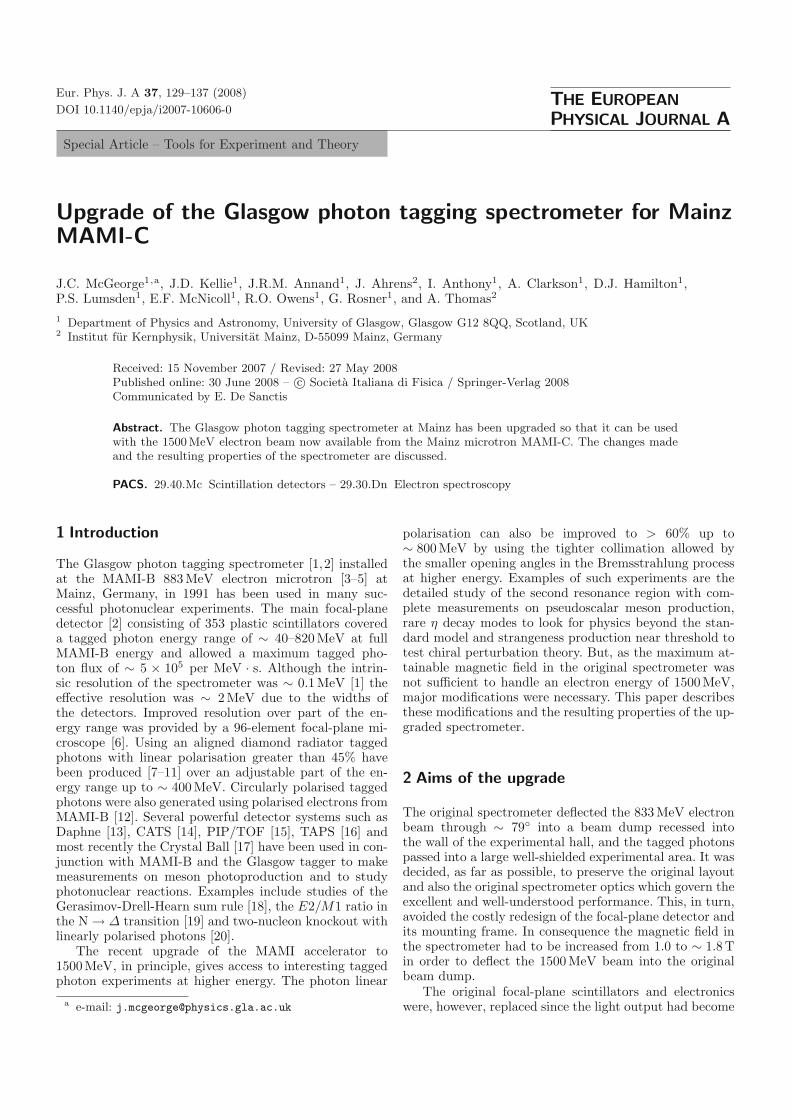
The original spectrometer deflected the 833MeV electronbeam through ∼ 79◦ into a beam dump recessed intothe wall of the experimental hall, and the tagged photonspassed into a large well-shielded experimental area. It wasdecided, as far as possible, to preserve the original layoutand also the original spectrometer optics which govern theexcellent and well-understood performance. This, in turn,avoided the costly redesign of the focal-plane detector andits mounting frame. In consequence the magnetic field inthe spectrometer had to be increased from 1.0 to ∼ 1.8Tin order to deflect the 1500MeV beam into the originalbeam dump.
The original focal-plane scintillators and electronicswere, however, replaced since the light output had become
130 The European Physical Journal A
Fig. 1. The upgraded photon tagging spectrometer: 3D view(upper part) and cross-section (lower part).
reduced, typically by a factor greater than 10, due to ra-diation damage and the original electronics had becomeobsolete and incompatible with the CATCH [21] electron-ics used with the Crystal Ball detector system. As the de-tector geometry was not changed the effective resolutionbecomes ∼ 4MeV when tagging at 1500MeV.
3 Upgrade of the spectrometer magnet
The existing power supply and cooling arrangements forthe magnet coils allowed for a current up to 440A whichproduced a field of 1.4T [1]. Simple estimates suggestedthat 1.8T could be obtained by reducing the pole gap aslong as the iron in the return yoke was increased in thick-ness to prevent saturation. Reducing the pole gap is per-missible since angles associated with the Bremsstrahlungprocess scale approximately as 1/energy, and a reduc-tion from 50mm (for 883MeV) to 25mm (for 1500MeV)does not appreciably increase the fraction of the post-Bremsstrahlung electrons (tagging electrons) which hitthe pole faces of the magnet. With a 25mm pole gap and110mm extra return yoke thickness (fig. 1), calculationsusing the finite element code TOSCA [22] showed that anaverage field of ∼ 1.96T would be reached with a currentof 440A. Therefore new additional top, bottom and backyokes were fabricated, each of thickness 110mm.
Measurements [1] had shown that the maximum polegap distortion in the original spectrometer was 0.14mm ata field of 1.0T, and this could be expected to increase to∼ 0.54mm at 1.96T. Some estimates of the stresses anddistortions involved were made by finite element modelling(FEM) of the original and upgraded spectrometers as solidstructures using the IDEAS [23] and ABAQUS [24] pro-grams. The upgraded spectrometer was strengthened by
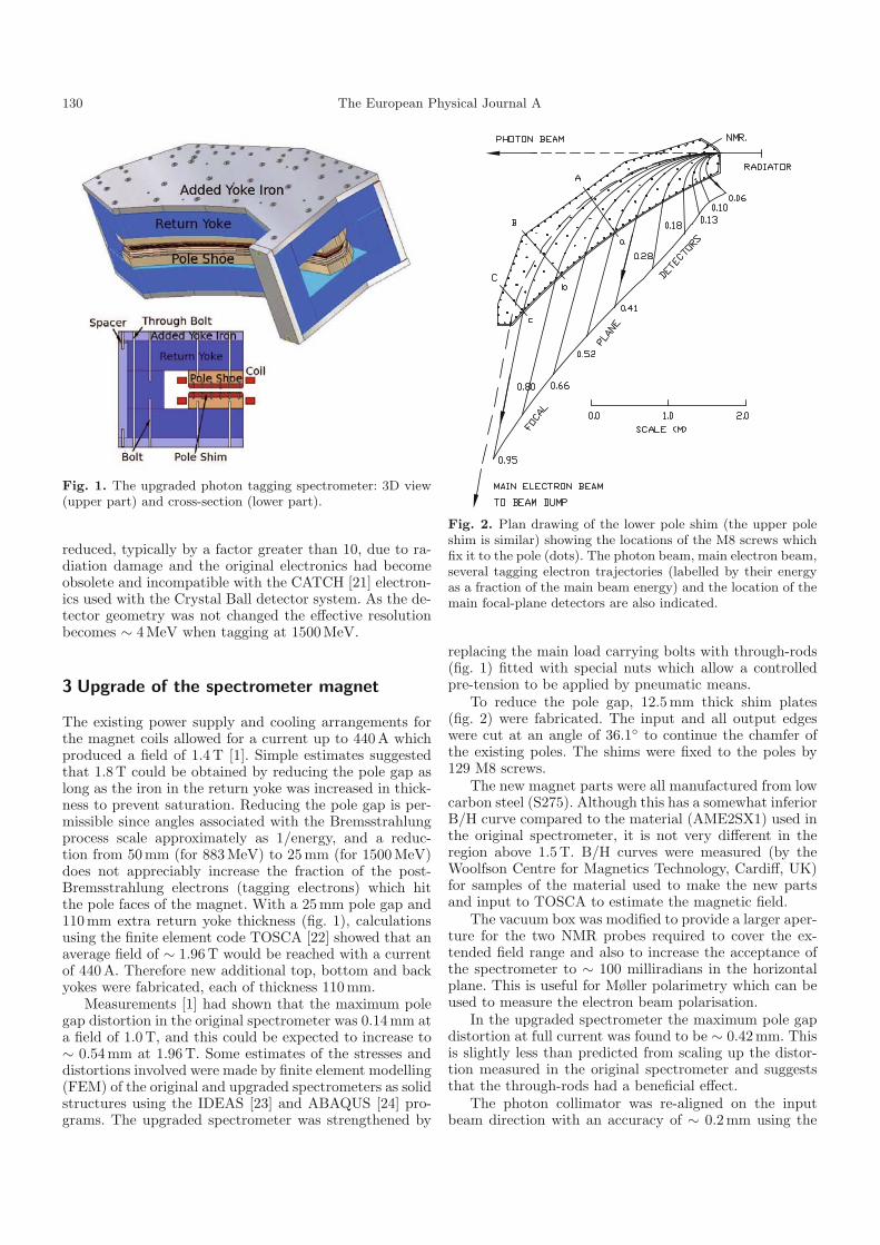
Fig. 2. Plan drawing of the lower pole shim (the upper poleshim is similar) showing the locations of the M8 screws whichfix it to the pole (dots). The photon beam, main electron beam,several tagging electron trajectories (labelled by their energyas a fraction of the main beam energy) and the location of themain focal-plane detectors are also indicated.
replacing the main load carrying bolts with through-rods(fig. 1) fitted with special nuts which allow a controlledpre-tension to be applied by pneumatic means.
To reduce the pole gap, 12.5mm thick shim plates(fig. 2) were fabricated. The input and all output edgeswere cut at an angle of 36.1◦ to continue the chamfer ofthe existing poles. The shims were fixed to the poles by129 M8 screws.
The new magnet parts were all manufactured from lowcarbon steel (S275). Although this has a somewhat inferiorB/H curve compared to the material (AME2SX1) used inthe original spectrometer, it is not very different in theregion above 1.5T. B/H curves were measured (by theWoolfson Centre for Magnetics Technology, Cardiff, UK)for samples of the material used to make the new partsand input to TOSCA to estimate the magnetic field.
The vacuum box was modified to provide a larger aper-ture for the two NMR probes required to cover the ex-tended field range and also to increase the acceptance ofthe spectrometer to ∼ 100 milliradians in the horizontalplane. This is useful for Møller polarimetry which can beused to measure the electron beam polarisation.
In the upgraded spectrometer the maximum pole gapdistortion at full current was found to be ∼ 0.42mm. Thisis slightly less than predicted from scaling up the distor-tion measured in the original spectrometer and suggeststhat the through-rods had a beneficial effect.
The photon collimator was re-aligned on the inputbeam direction with an accuracy of ∼ 0.2mm using the
J.C. McGeorge et al.: Tagger upgrade 131
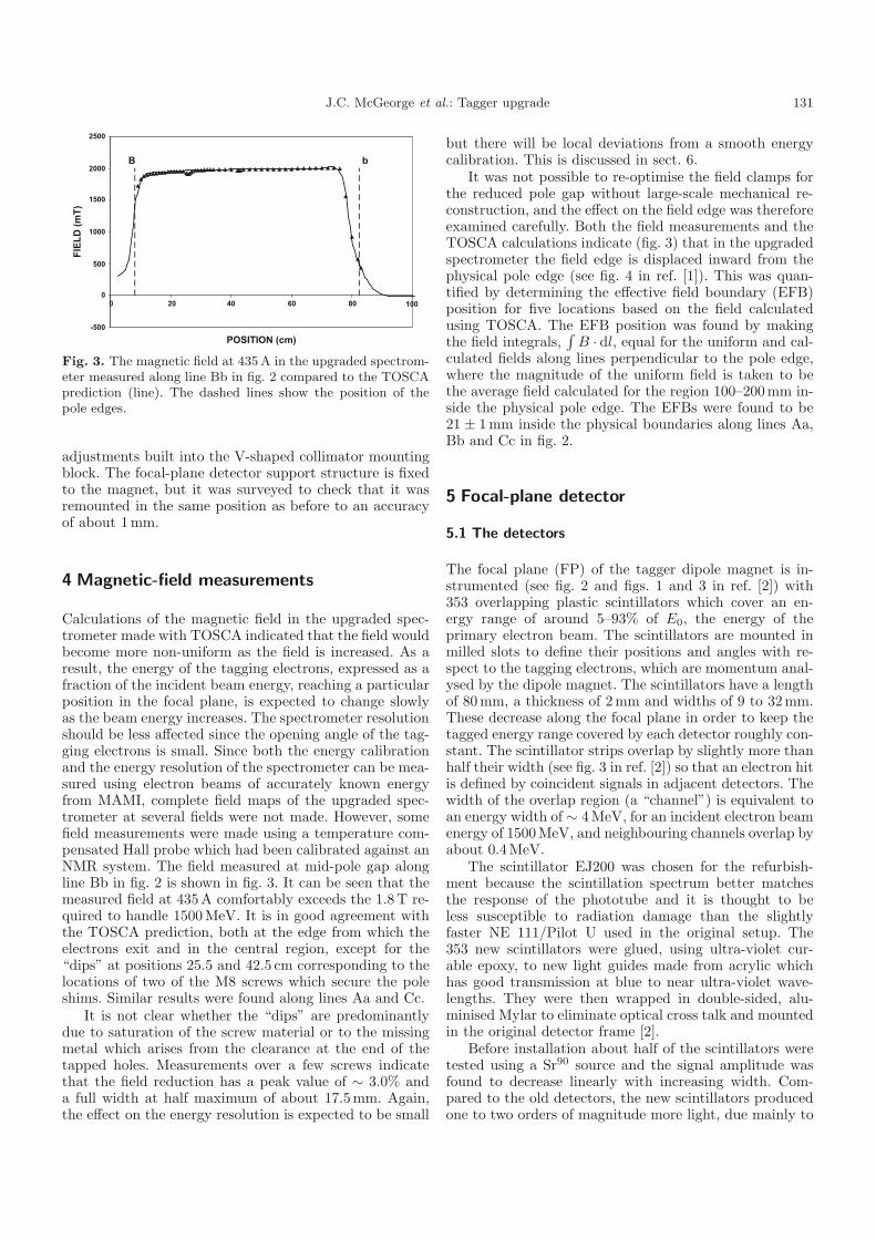
Fig. 3. The magnetic field at 435 A in the upgraded spectrom-eter measured along line Bb in fig. 2 compared to the TOSCAprediction (line). The dashed lines show the position of thepole edges.
adjustments built into the V-shaped collimator mountingblock. The focal-plane detector support structure is fixedto the magnet, but it was surveyed to check that it wasremounted in the same position as before to an accuracyof about 1mm.
4 Magnetic-field measurements
Calculations of the magnetic field in the upgraded spec-trometer made with TOSCA indicated that the field wouldbecome more non-uniform as the field is increased. As aresult, the energy of the tagging electrons, expressed as afraction of the incident beam energy, reaching a particularposition in the focal plane, is expected to change slowlyas the beam energy increases. The spectrometer resolutionshould be less affected since the opening angle of the tag-ging electrons is small. Since both the energy calibrationand the energy resolution of the spectrometer can be mea-sured using electron beams of accurately known energyfrom MAMI, complete field maps of the upgraded spec-trometer at several fields were not made. However, somefield measurements were made using a temperature com-pensated Hall probe which had been calibrated against anNMR system. The field measured at mid-pole gap alongline Bb in fig. 2 is shown in fig. 3. It can be seen that themeasured field at 435A comfortably exceeds the 1.8T re-quired to handle 1500MeV. It is in good agreement withthe TOSCA prediction, both at the edge from which theelectrons exit and in the central region, except for the“dips” at positions 25.5 and 42.5 cm corresponding to thelocations of two of the M8 screws which secure the poleshims. Similar results were found along lines Aa and Cc.
It is not clear whether the “dips” are predominantlydue to saturation of the screw material or to the missingmetal which arises from the clearance at the end of thetapped holes. Measurements over a few screws indicatethat the field reduction has a peak value of ∼ 3.0% anda full width at half maximum of about 17.5mm. Again,the effect on the energy resolution is expected to be small
but there will be local deviations from a smooth energycalibration. This is discussed in sect. 6.
It was not possible to re-optimise the field clamps forthe reduced pole gap without large-scale mechanical re-construction, and the effect on the field edge was thereforeexamined carefully. Both the field measurements and theTOSCA calculations indicate (fig. 3) that in the upgradedspectrometer the field edge is displaced inward from thephysical pole edge (see fig. 4 in ref. [1]). This was quan-tified by determining the effective field boundary (EFB)position for five locations based on the field calculatedusing TOSCA. The EFB position was found by makingthe field integrals,
∫B · dl, equal for the uniform and cal-
culated fields along lines perpendicular to the pole edge,where the magnitude of the uniform field is taken to bethe average field calculated for the region 100–200mm in-side the physical pole edge. The EFBs were found to be21 ± 1mm inside the physical boundaries along lines Aa,Bb and Cc in fig. 2.
5 Focal-plane detector
5.1 The detectors
The focal plane (FP) of the tagger dipole magnet is in-strumented (see fig. 2 and figs. 1 and 3 in ref. [2]) with353 overlapping plastic scintillators which cover an en-ergy range of around 5–93% of E0, the energy of theprimary electron beam. The scintillators are mounted inmilled slots to define their positions and angles with re-spect to the tagging electrons, which are momentum anal-ysed by the dipole magnet. The scintillators have a lengthof 80mm, a thickness of 2mm and widths of 9 to 32mm.These decrease along the focal plane in order to keep thetagged energy range covered by each detector roughly con-stant. The scintillator strips overlap by slightly more thanhalf their width (see fig. 3 in ref. [2]) so that an electron hitis defined by coincident signals in adjacent detectors. Thewidth of the overlap region (a “channel”) is equivalent toan energy width of ∼ 4MeV, for an incident electron beamenergy of 1500MeV, and neighbouring channels overlap byabout 0.4MeV.
The scintillator EJ200 was chosen for the refurbish-ment because the scintillation spectrum better matchesthe response of the phototube and it is thought to beless susceptible to radiation damage than the slightlyfaster NE 111/Pilot U used in the original setup. The353 new scintillators were glued, using ultra-violet cur-able epoxy, to new light guides made from acrylic whichhas good transmission at blue to near ultra-violet wave-lengths. They were then wrapped in double-sided, alu-minised Mylar to eliminate optical cross talk and mountedin the original detector frame [2].
Before installation about half of the scintillators weretested using a Sr90 source and the signal amplitude wasfound to decrease linearly with increasing width. Com-pared to the old detectors, the new scintillators producedone to two orders of magnitude more light, due mainly to
132 The European Physical Journal A
A A A
−
−B
B
D
D
D
C C
C
Voltage divider for R1635 10mm PM
+
−
660k 330k
+
−
+
−
Vmax −1.5kV
3301k330150330150
−5−5
+5 +5+5
−5
−1.1 kV
To QDC
4.7
+
+
1k
1.2k1k 1k
LE1k
Clk
R
SD Q
QClk
R
SD Q
Q
Clk
R
SD Q
Q
51R1k
1k 1k8
FP channel n
To FP n+1
5ns
5ns
5ns
LVDS
100 n
4.7
1.2k
51
51
+5
+3.
3
4.7
−5
−5
+3.3
+3.3 +1.3
+1.3 1k
51
+3.3
100 n
330
330
100 n+1.3
5151
51
+3.3 +1.3
51
+3.3 47
82 47
+3.3
10 n
10 n
High Threshold
Low Threshold
−551
100 n
51
Voltage Comparators
NIM
Cable
10ns
+1.3
+5LE
−5From FP n−1
( n, n−1 coincidence )
82
0.05" Pitch
10n 10n
D1 D8D7D6D5D4D3 AD3D2K
10M
125V
250 V
10n
330k 330k 330k 330k 330k
330k
10k
51 5151
FP scintillator HV/Discriminator Circuit
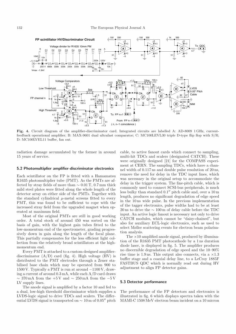
Fig. 4. Circuit diagram of the amplifier-discriminator card. Integrated circuits are labelled A: AD-8009 1 GHz, current-feedback operational amplifier; B: MAX-9601 dual ultrafast comparator; C: MC100LEVL30 triple D-type flip flop with S/R;D: MC100LVEL11 buffer, fan out.
radiation damage accumulated by the former in around15 years of service.
5.2 Photomultiplier amplifier-discriminator electronics
Each scintillator on the FP is fitted with a HamamatsuR1635 photomultiplier tube (PMT). As the PMTs are af-fected by stray fields of more than ∼ 0.01T, 0.7mm thickmild steel plates were fitted along the whole length of thedetector array on either side of the PMTs. Together withthe standard cylindrical μ-metal screens fitted to everyPMT, this was found to be sufficient to cope with theincreased stray field from the upgraded magnet when op-erated at maximum field.
Most of the original PMTs are still in good workingorder. A total stock of around 450 was sorted on thebasis of gain, with the highest gain tubes fitted to thelow-momentum end of the spectrometer, grading progres-sively down in gain along the length of the focal plane.This partially compensates for the less efficient light col-lection from the relatively broad scintillators at the high-momentum end.
Every PMT is attached to a custom designed amplifier-discriminator (A/D) card (fig. 4). High voltage (HV) isdistributed to the PMT electrodes through a Zener sta-bilised base chain which may be operated from 900 to1500 V. Typically a PMT is run at around −1100V, draw-ing a current of around 0.3mA, while each A/D card draws∼ 370mA from the +5V and ∼ 250mA from the −5VLV supply lines.
The anode signal is amplified by a factor 10 and fed toa dual, low-high threshold discriminator which supplies aLVDS-logic signal to drive TDCs and scalers. The differ-ential LVDS signal is transported on ∼ 10m of 0.05′′ pitch
cable, to active fanout cards which connect to sampling,multi-hit TDCs and scalers (designated CATCH). Thesewere originally designed [21] for the COMPASS experi-ment at CERN. The sampling TDCs, which have a chan-nel width of 0.117 ns and double pulse resolution of 20 ns,remove the need for delay in the TDC input lines, whichwas necessary in the original setup to accommodate thedelay in the trigger system. The fine-pitch cable, which iscommonly used to connect SCSI-bus peripherals, is muchless bulky than standard 0.1′′ pitch cable and, over a 10mlength, produces no significant degradation of edge speedin the 10 ns wide pulse. In the previous implementationof the tagger electronics, pulse widths had to be at least20 ns to drive the ∼ 100m of delay cable before the TDCinput. An active logic fanout is necessary not only to driveCATCH modules, which cannot be “daisy-chained”, butalso for auxiliary ECL-logic electronics, such as used toselect Møller scattering events for electron beam polarisa-tion analysis.
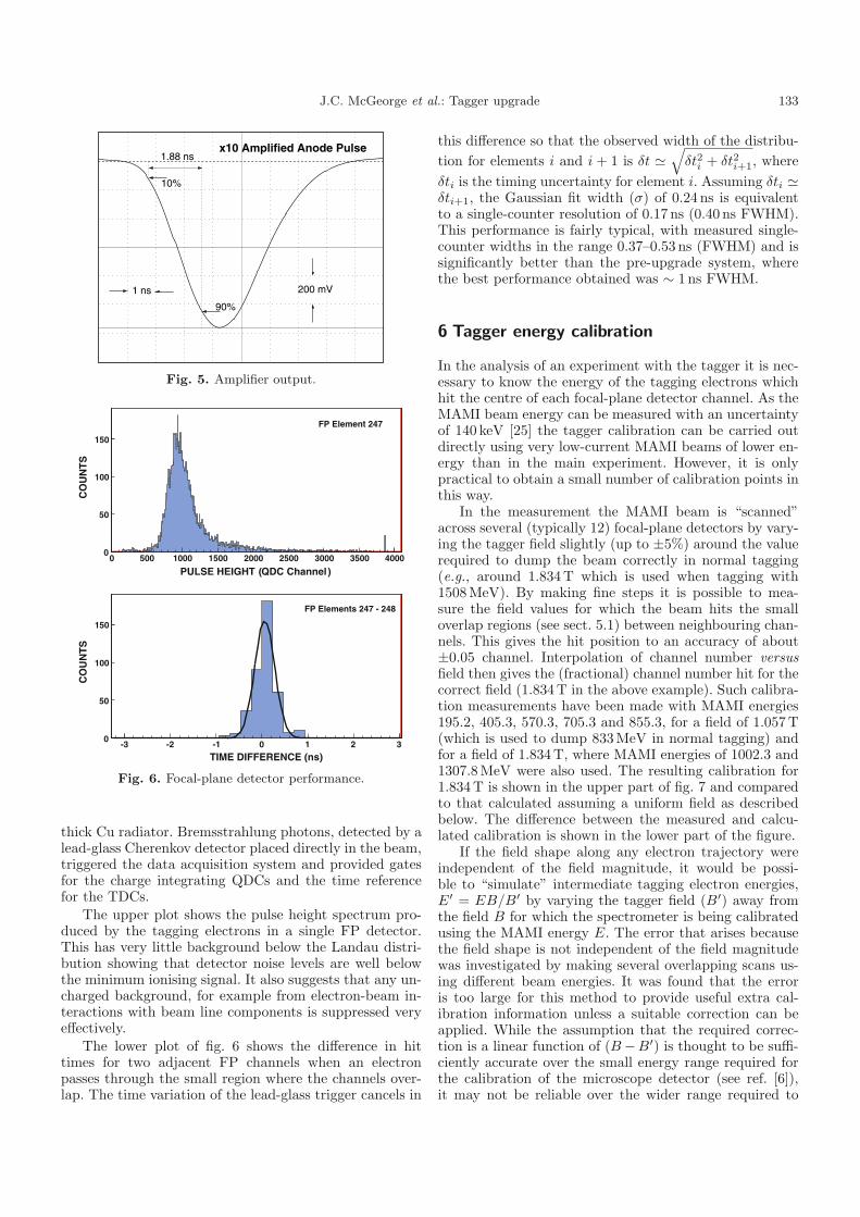
The ×10 amplified anode signal, produced by illumina-tion of the R1635 PMT photocathode by a 1 ns durationdiode laser, is displayed in fig. 5. The amplifier producesno discernible degradation of edge speed and the 10–90%rise time is 1.9 ns. This output also connects, via a ×1.3buffer stage and a coaxial delay line, to a LeCroy 1885FFASTBUS QDC which is normally read out during HVadjustment to align FP detector gains.
5.3 Detector performance
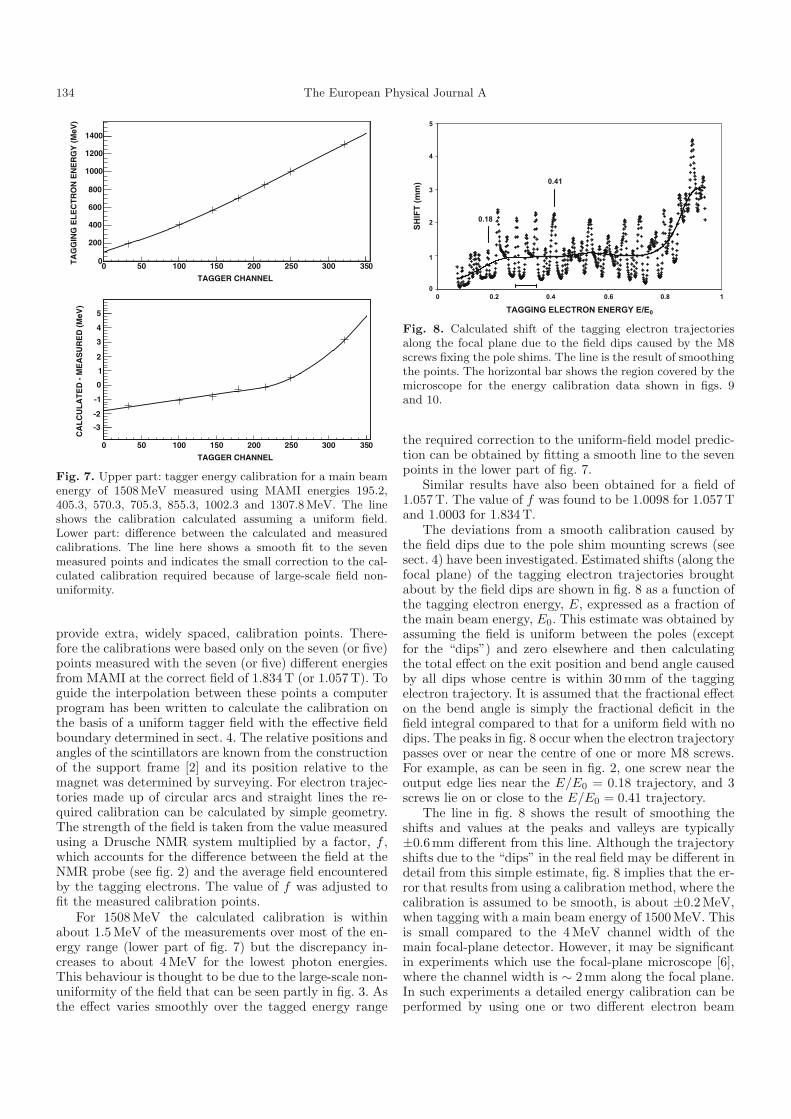
The performance of the FP detectors and electronics isillustrated in fig. 6 which displays spectra taken with theMAMI-C 1508MeV electron beam incident on a 10 micron
J.C. McGeorge et al.: Tagger upgrade 133
1 ns 200 mV
1.88 ns
90%
10%
x10 Amplified Anode Pulse
Fig. 5. Amplifier output.
PULSE HEIGHT (QDC Channel)0 500 1000 1500 2000 2500 3000 3500 4000
CO
UN
TS
0
50
100
150
FP Element 247
TIME DIFFERENCE (ns)-3 -2 -1 0 1 2 3
CO
UN
TS
0
50
100
150
FP Elements 247 - 248
Fig. 6. Focal-plane detector performance.
thick Cu radiator. Bremsstrahlung photons, detected by alead-glass Cherenkov detector placed directly in the beam,triggered the data acquisition system and provided gatesfor the charge integrating QDCs and the time referencefor the TDCs.
The upper plot shows the pulse height spectrum pro-duced by the tagging electrons in a single FP detector.This has very little background below the Landau distri-bution showing that detector noise levels are well belowthe minimum ionising signal. It also suggests that any un-charged background, for example from electron-beam in-teractions with beam line components is suppressed veryeffectively.
The lower plot of fig. 6 shows the difference in hittimes for two adjacent FP channels when an electronpasses through the small region where the channels over-lap. The time variation of the lead-glass trigger cancels in
this difference so that the observed width of the distribu-
tion for elements i and i + 1 is δt �√
δt2i + δt2i+1, where
δti is the timing uncertainty for element i. Assuming δti �δti+1, the Gaussian fit width (σ) of 0.24 ns is equivalentto a single-counter resolution of 0.17 ns (0.40 ns FWHM).This performance is fairly typical, with measured single-counter widths in the range 0.37–0.53 ns (FWHM) and issignificantly better than the pre-upgrade system, wherethe best performance obtained was ∼ 1 ns FWHM.
6 Tagger energy calibration
In the analysis of an experiment with the tagger it is nec-essary to know the energy of the tagging electrons whichhit the centre of each focal-plane detector channel. As theMAMI beam energy can be measured with an uncertaintyof 140 keV [25] the tagger calibration can be carried outdirectly using very low-current MAMI beams of lower en-ergy than in the main experiment. However, it is onlypractical to obtain a small number of calibration points inthis way.
In the measurement the MAMI beam is “scanned”across several (typically 12) focal-plane detectors by vary-ing the tagger field slightly (up to ±5%) around the valuerequired to dump the beam correctly in normal tagging(e.g., around 1.834T which is used when tagging with1508MeV). By making fine steps it is possible to mea-sure the field values for which the beam hits the smalloverlap regions (see sect. 5.1) between neighbouring chan-nels. This gives the hit position to an accuracy of about±0.05 channel. Interpolation of channel number versus
field then gives the (fractional) channel number hit for thecorrect field (1.834T in the above example). Such calibra-tion measurements have been made with MAMI energies195.2, 405.3, 570.3, 705.3 and 855.3, for a field of 1.057T(which is used to dump 833MeV in normal tagging) andfor a field of 1.834T, where MAMI energies of 1002.3 and1307.8MeV were also used. The resulting calibration for1.834T is shown in the upper part of fig. 7 and comparedto that calculated assuming a uniform field as describedbelow. The difference between the measured and calcu-lated calibration is shown in the lower part of the figure.
If the field shape along any electron trajectory wereindependent of the field magnitude, it would be possi-ble to “simulate” intermediate tagging electron energies,E′ = EB/B′ by varying the tagger field (B′) away fromthe field B for which the spectrometer is being calibratedusing the MAMI energy E. The error that arises becausethe field shape is not independent of the field magnitudewas investigated by making several overlapping scans us-ing different beam energies. It was found that the erroris too large for this method to provide useful extra cal-ibration information unless a suitable correction can beapplied. While the assumption that the required correc-tion is a linear function of (B−B′) is thought to be suffi-ciently accurate over the small energy range required forthe calibration of the microscope detector (see ref. [6]),it may not be reliable over the wider range required to
134 The European Physical Journal A
TAGGER CHANNEL
0 50 100 150 200 250 300 350TA
GG
ING
EL
EC
TR
ON
EN
ER
GY
(M
eV)
0
200
400
600
800
1000
1200
1400
CA
LC
UL
AT
ED
- M
EA
SU
RE
D (
MeV
)
-3
-2
-1
0
1
2
3
4
5
TAGGER CHANNEL
0 50 100 150 200 250 300 350
Fig. 7. Upper part: tagger energy calibration for a main beamenergy of 1508 MeV measured using MAMI energies 195.2,405.3, 570.3, 705.3, 855.3, 1002.3 and 1307.8 MeV. The lineshows the calibration calculated assuming a uniform field.Lower part: difference between the calculated and measuredcalibrations. The line here shows a smooth fit to the sevenmeasured points and indicates the small correction to the cal-culated calibration required because of large-scale field non-uniformity.
provide extra, widely spaced, calibration points. There-fore the calibrations were based only on the seven (or five)points measured with the seven (or five) different energiesfrom MAMI at the correct field of 1.834T (or 1.057T). Toguide the interpolation between these points a computerprogram has been written to calculate the calibration onthe basis of a uniform tagger field with the effective fieldboundary determined in sect. 4. The relative positions andangles of the scintillators are known from the constructionof the support frame [2] and its position relative to themagnet was determined by surveying. For electron trajec-tories made up of circular arcs and straight lines the re-quired calibration can be calculated by simple geometry.The strength of the field is taken from the value measuredusing a Drusche NMR system multiplied by a factor, f ,which accounts for the difference between the field at theNMR probe (see fig. 2) and the average field encounteredby the tagging electrons. The value of f was adjusted tofit the measured calibration points.
For 1508MeV the calculated calibration is withinabout 1.5MeV of the measurements over most of the en-ergy range (lower part of fig. 7) but the discrepancy in-creases to about 4MeV for the lowest photon energies.This behaviour is thought to be due to the large-scale non-uniformity of the field that can be seen partly in fig. 3. Asthe effect varies smoothly over the tagged energy range
Fig. 8. Calculated shift of the tagging electron trajectoriesalong the focal plane due to the field dips caused by the M8screws fixing the pole shims. The line is the result of smoothingthe points. The horizontal bar shows the region covered by themicroscope for the energy calibration data shown in figs. 9and 10.
the required correction to the uniform-field model predic-tion can be obtained by fitting a smooth line to the sevenpoints in the lower part of fig. 7.
Similar results have also been obtained for a field of1.057T. The value of f was found to be 1.0098 for 1.057Tand 1.0003 for 1.834T.
The deviations from a smooth calibration caused bythe field dips due to the pole shim mounting screws (seesect. 4) have been investigated. Estimated shifts (along thefocal plane) of the tagging electron trajectories broughtabout by the field dips are shown in fig. 8 as a function ofthe tagging electron energy, E, expressed as a fraction ofthe main beam energy, E0. This estimate was obtained byassuming the field is uniform between the poles (exceptfor the “dips”) and zero elsewhere and then calculatingthe total effect on the exit position and bend angle causedby all dips whose centre is within 30mm of the taggingelectron trajectory. It is assumed that the fractional effecton the bend angle is simply the fractional deficit in thefield integral compared to that for a uniform field with nodips. The peaks in fig. 8 occur when the electron trajectorypasses over or near the centre of one or more M8 screws.For example, as can be seen in fig. 2, one screw near theoutput edge lies near the E/E0 = 0.18 trajectory, and 3screws lie on or close to the E/E0 = 0.41 trajectory.
The line in fig. 8 shows the result of smoothing theshifts and values at the peaks and valleys are typically±0.6mm different from this line. Although the trajectoryshifts due to the “dips” in the real field may be different indetail from this simple estimate, fig. 8 implies that the er-ror that results from using a calibration method, where thecalibration is assumed to be smooth, is about ±0.2MeV,when tagging with a main beam energy of 1500MeV. Thisis small compared to the 4MeV channel width of themain focal-plane detector. However, it may be significantin experiments which use the focal-plane microscope [6],where the channel width is ∼ 2mm along the focal plane.In such experiments a detailed energy calibration can beperformed by using one or two different electron beam
J.C. McGeorge et al.: Tagger upgrade 135
Fig. 9. Energy calibration in the region E/E0 = 0.27–0.35 (forE0 = 883 MeV) obtained from scanning a 270.17 MeV beamfrom MAMI across the microscope by varying the tagger field.The line shows the result of a calculation assuming a uniformfield.
Fig. 10. Difference between the measured and calculated mi-croscope calibrations shown in fig. 9. The line shows the cal-culated difference (see text) based on the appropriate sectionof fig. 8.
energies from MAMI and “scanning” them across the mi-croscope by making small variations in the magnetic fieldin the spectrometer (see ref. [6]).
Such a scan can also be used to look for the effects ofthe shifts predicted in fig. 8 over the small range coveredby the microscope detector. This has been done with themicroscope covering the range E/E0 = 0.27–0.35 (indi-cated by the horizontal bar in fig. 8). In fig. 9 the mea-sured microscope calibration points are compared to thecalibration calculated assuming a uniform field and usingthe known microscope geometry. As the microscope po-sition and angle were not known with sufficient precisionthese were adjusted in the calculation to fit the measuredpoints. The difference between the measured points andthe calculation is shown in detail in fig. 10. The line in thisfigure shows the difference between the original points andsmoothed line in the relevant section of fig. 8. The agree-ment in fig. 10 is good enough to give some confidencein the estimate, made above, of the energy calibration er-ror arising from the assumption that the calibration issmooth.
Including the uncertainty in the MAMI beam energy,the uncertainty in the seven calibration points (measuredfor tagging at a main beam energy of 1508MeV) is esti-mated to be about ±0.3MeV. Measurements of the poleshim thicknesses suggest that small variations in the polegap could cause slight structure in the calibration betweenthe measured points. Including this, it is estimated thatthe error in the calculated calibration, after correction forlarge-scale field non-uniformity using the fit shown in thelower part of fig. 7, is about ±0.5MeV for channels up to∼ 270. It could be significantly larger for lower tagged pho-ton energies where the shape of the correction is less welldefined. There is also an additional uncertainty caused bythe field dips. From fig. 8, this is estimated to be typicallyabout ±0.2MeV.
7 The performance of the upgraded
spectrometer
The intrinsic resolution of the upgraded spectrometer wasmeasured at a field of 1.95T which made an 855MeVbeam from MAMI hit the microscope detector placed nearthe middle of the focal plane. Multiple scattering in a2mm thick Al sheet placed in the beam at the radiator po-sition was used to simulate the opening-angle distributionof tagging electrons. From the distribution of electrons hit-ting a small number of microscope channels the resolutionwas found to be ∼ 0.4MeV FWHM. This is an overesti-mate because the opening angles in this test were about3 times bigger than is the case for the tagging electronsfrom a typical radiator at 1508MeV main beam energy.It shows that when the main focal-plane detector is usedits channel width (∼ 4MeV) dominates the tagged energyresolution. For some experiments which make use of thefocal-plane microscope, however, it may be necessary tomake more careful measurements of the resolution.
Measurements of the “tagging efficiency”, that is thefraction of the tagged photons which pass through thecollimator, were made at reduced beam current using a25 cm3 lead-glass Cherenkov detector placed on the pho-ton beam line. The results from a measurement using a10 micron thick Cu radiator and a 4mm diameter collima-tor are shown in fig. 11. The measured tagging efficiencywas found to be significantly smaller than predicted by aMonte Carlo calculation which includes the input beamdivergence and diameter, multiple scattering in the radi-ator, the Bremsstrahlung photon opening-angle distribu-tion and the effect of Møller electron scattering. A similardiscrepancy was also found using a collimator diameterof 3mm and a 6 micron thick Ta radiator. Although notfully understood, much of the discrepancy may be due toslight misalignment of the collimator. The measured tag-ging efficiency is, however, stable and reproducible. Mea-surements made several months apart averaged over alltagger channels agree to better than 1%.
As a test of the focal-plane detector background, thecount rate was measured with no radiator in the beam. Itwas found to be about 5 × 10⁻⁵ times smaller than therate with a 10 micron thick Cu radiator in the beam.
136 The European Physical Journal A
Fig. 11. Tagging efficiency measured at a main beam energyof 1508 MeV using a 10 micron thick Cu radiator and a 4 mmdiameter collimator. The line shows the result of a Monte Carlocalculation.
TAGGER CHANNEL0 50 100 150 200 250 300 350
CO
UN
TS
0
0.5
1
1.5
2
2.5
3
3.5310×
PHOTON ENERGY (MeV)1000 500 2507501250
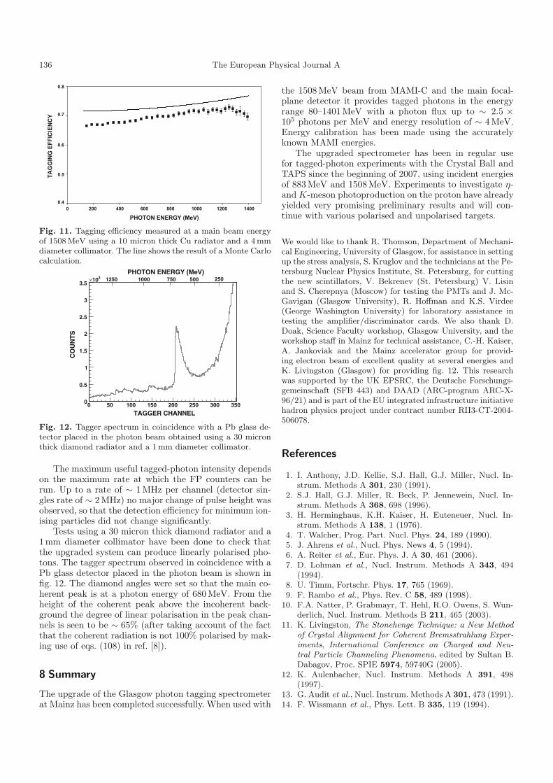
Fig. 12. Tagger spectrum in coincidence with a Pb glass de-tector placed in the photon beam obtained using a 30 micronthick diamond radiator and a 1 mm diameter collimator.
The maximum useful tagged-photon intensity dependson the maximum rate at which the FP counters can berun. Up to a rate of ∼ 1MHz per channel (detector sin-gles rate of ∼ 2MHz) no major change of pulse height wasobserved, so that the detection efficiency for minimum ion-ising particles did not change significantly.
Tests using a 30 micron thick diamond radiator and a1mm diameter collimator have been done to check thatthe upgraded system can produce linearly polarised pho-tons. The tagger spectrum observed in coincidence with aPb glass detector placed in the photon beam is shown infig. 12. The diamond angles were set so that the main co-herent peak is at a photon energy of 680MeV. From theheight of the coherent peak above the incoherent back-ground the degree of linear polarisation in the peak chan-nels is seen to be ∼ 65% (after taking account of the factthat the coherent radiation is not 100% polarised by mak-ing use of eqs. (108) in ref. [8]).
8 Summary
The upgrade of the Glasgow photon tagging spectrometerat Mainz has been completed successfully. When used with
the 1508MeV beam from MAMI-C and the main focal-plane detector it provides tagged photons in the energyrange 80–1401MeV with a photon flux up to ∼ 2.5 ×10⁵ photons per MeV and energy resolution of ∼ 4MeV.Energy calibration has been made using the accuratelyknown MAMI energies.
The upgraded spectrometer has been in regular usefor tagged-photon experiments with the Crystal Ball andTAPS since the beginning of 2007, using incident energiesof 883MeV and 1508MeV. Experiments to investigate η-and K-meson photoproduction on the proton have alreadyyielded very promising preliminary results and will con-tinue with various polarised and unpolarised targets.
We would like to thank R. Thomson, Department of Mechani-cal Engineering, University of Glasgow, for assistance in settingup the stress analysis, S. Kruglov and the technicians at the Pe-tersburg Nuclear Physics Institute, St. Petersburg, for cuttingthe new scintillators, V. Bekrenev (St. Petersburg) V. Lisinand S. Cherepnya (Moscow) for testing the PMTs and J. Mc-Gavigan (Glasgow University), R. Hoffman and K.S. Virdee(George Washington University) for laboratory assistance intesting the amplifier/discriminator cards. We also thank D.Doak, Science Faculty workshop, Glasgow University, and theworkshop staff in Mainz for technical assistance, C.-H. Kaiser,A. Jankoviak and the Mainz accelerator group for provid-ing electron beam of excellent quality at several energies andK. Livingston (Glasgow) for providing fig. 12. This researchwas supported by the UK EPSRC, the Deutsche Forschungs-gemeinschaft (SFB 443) and DAAD (ARC-program ARC-X-96/21) and is part of the EU integrated infrastructure initiativehadron physics project under contract number RII3-CT-2004-506078.
References
1. I. Anthony, J.D. Kellie, S.J. Hall, G.J. Miller, Nucl. In-strum. Methods A 301, 230 (1991).
2. S.J. Hall, G.J. Miller, R. Beck, P. Jennewein, Nucl. In-strum. Methods A 368, 698 (1996).
3. H. Herminghaus, K.H. Kaiser, H. Euteneuer, Nucl. In-strum. Methods A 138, 1 (1976).
4. T. Walcher, Prog. Part. Nucl. Phys. 24, 189 (1990).5. J. Ahrens et al., Nucl. Phys. News 4, 5 (1994).6. A. Reiter et al., Eur. Phys. J. A 30, 461 (2006).7. D. Lohman et al., Nucl. Instrum. Methods A 343, 494
(1994).8. U. Timm, Fortschr. Phys. 17, 765 (1969).9. F. Rambo et al., Phys. Rev. C 58, 489 (1998).
10. F.A. Natter, P. Grabmayr, T. Hehl, R.O. Owens, S. Wun-derlich, Nucl. Instrum. Methods B 211, 465 (2003).
11. K. Livingston, The Stonehenge Technique: a New Method
of Crystal Alignment for Coherent Bremsstrahlung Exper-
iments, International Conference on Charged and Neu-
tral Particle Channeling Phenomena, edited by Sultan B.Dabagov, Proc. SPIE 5974, 59740G (2005).
12. K. Aulenbacher, Nucl. Instrum. Methods A 391, 498(1997).
13. G. Audit et al., Nucl. Instrum. Methods A 301, 473 (1991).14. F. Wissmann et al., Phys. Lett. B 335, 119 (1994).

J.C. McGeorge et al.: Tagger upgrade 137
15. I.J.D. MacGregor et al., Nucl. Instrum. Methods A 382,479 (1996); P. Grabmayr et al., Nucl. Instrum. Methods A402, 85 (1998).
16. R. Novotny, IEEE Trans. Nucl. Science, 38, 379 (1991).17. M. Oreglia et al., Phys. Rev. D 25, 2259 (1982); S.
Starostin et al., Phys. Rev. C 64, 055205 (2001).18. J. Ahrens et al., Phys. Rev. Lett. 87, 02203 (2001).19. R. Beck et al., Phys. Rev. Lett. 78, 606 (1997).20. C.J.Y. Powrie et al., Phys. Rev. C 64, 034602 (2001); S.
Franczuk et al., Phys. Lett. B 450, 332 (1999).21. A common readout driver for the COMPASS experiment,
T. Schmidt, PhD Thesis, Albert-Ludwigs-Universitat,Freiburg, May 2002.
22. A.G.A.M Armstrong, C.P. Riley, J. Simkin, TOSCA:3D Static Electromagnetic/Electrostatic Analysis Pack-age, RL-81-070, Rutherford Appleton Laboratory, 1982;TOSCA: 3D Magnetic Field Computation, Vector FieldsLtd., 24 Bankside, Kidlington, Oxford, UK.
23. SDRC Inc., Cincinnati, OH, USA.24. Hibbett, Karlsson, Sorenson Inc., Pawtucket, RI, USA.25. K.-H. Kaiser, private communication; A. Jankoviak
et al., Eur. Phys. J. A 28, s01, 149 (2006) DOI:10.1140/epja/i2006-09-016-3.