Embed Size (px)
Citation preview

University of Warwick institutional repository: http://go.warwick.ac.uk/wrap
A Thesis Submitted for the Degree of PhD at the University of Warwick
http://go.warwick.ac.uk/wrap/57699
This thesis is made available online and is protected by original copyright.
Please scroll down to view the document itself.
Please refer to the repository record for this item for information to help you to cite it. Our policy information is available from the repository home page.

Introducing the Hybrid UnipolarBipolar Field Effect Transistor:
The HUBFET
Benedict Thomas Donnellan
School of Engineering
University of Warwick
Dissertation submitted for the degree of
Doctor of Philosophy
February 2013

Contents
Nomenclature xiii
1 Introduction 11.1 Introduction . . . . . . . . . . . . . . . . . . . . . . . . . . . . . . . . . . . . 11.2 More electric aircraft . . . . . . . . . . . . . . . . . . . . . . . . . . . . . . . 21.3 Motivation . . . . . . . . . . . . . . . . . . . . . . . . . . . . . . . . . . . . . 31.4 Thesis scope . . . . . . . . . . . . . . . . . . . . . . . . . . . . . . . . . . . . 5
2 Aircraft design 72.1 Traditional aircraft power systems . . . . . . . . . . . . . . . . . . . . . . . . 7
2.1.1 Hydraulics . . . . . . . . . . . . . . . . . . . . . . . . . . . . . . . . . 82.1.2 Pneumatics . . . . . . . . . . . . . . . . . . . . . . . . . . . . . . . . 92.1.3 Electrical power . . . . . . . . . . . . . . . . . . . . . . . . . . . . . . 92.1.4 More electric aircraft power systems . . . . . . . . . . . . . . . . . . . 10
2.2 MEA electrical power system . . . . . . . . . . . . . . . . . . . . . . . . . . 122.2.1 Primary power . . . . . . . . . . . . . . . . . . . . . . . . . . . . . . 132.2.2 Secondary power . . . . . . . . . . . . . . . . . . . . . . . . . . . . . 142.2.3 Energy storage . . . . . . . . . . . . . . . . . . . . . . . . . . . . . . 142.2.4 Power switches . . . . . . . . . . . . . . . . . . . . . . . . . . . . . . 152.2.5 Fault detection . . . . . . . . . . . . . . . . . . . . . . . . . . . . . . 162.2.6 The solution . . . . . . . . . . . . . . . . . . . . . . . . . . . . . . . . 18
2.3 Summary . . . . . . . . . . . . . . . . . . . . . . . . . . . . . . . . . . . . . 20
3 Semiconductor switches 213.1 The ideal switch . . . . . . . . . . . . . . . . . . . . . . . . . . . . . . . . . . 223.2 The vertical power MOSFET . . . . . . . . . . . . . . . . . . . . . . . . . . 24
3.2.1 History . . . . . . . . . . . . . . . . . . . . . . . . . . . . . . . . . . . 243.2.2 Basic structure . . . . . . . . . . . . . . . . . . . . . . . . . . . . . . 253.2.3 Operation . . . . . . . . . . . . . . . . . . . . . . . . . . . . . . . . . 273.2.4 Fabrication . . . . . . . . . . . . . . . . . . . . . . . . . . . . . . . . 333.2.5 Vertical power MOSFET summary . . . . . . . . . . . . . . . . . . . 34
3.3 The superjunction MOSFET . . . . . . . . . . . . . . . . . . . . . . . . . . . 383.3.1 History . . . . . . . . . . . . . . . . . . . . . . . . . . . . . . . . . . . 383.3.2 Basic structure . . . . . . . . . . . . . . . . . . . . . . . . . . . . . . 38
i

CONTENTS
3.3.3 Operation . . . . . . . . . . . . . . . . . . . . . . . . . . . . . . . . . 403.3.4 Fabrication . . . . . . . . . . . . . . . . . . . . . . . . . . . . . . . . 403.3.5 Superjunction MOSFET summary . . . . . . . . . . . . . . . . . . . 41
3.4 The IGBT . . . . . . . . . . . . . . . . . . . . . . . . . . . . . . . . . . . . . 423.4.1 History . . . . . . . . . . . . . . . . . . . . . . . . . . . . . . . . . . . 423.4.2 Basic structure . . . . . . . . . . . . . . . . . . . . . . . . . . . . . . 423.4.3 Variations . . . . . . . . . . . . . . . . . . . . . . . . . . . . . . . . . 443.4.4 Operation . . . . . . . . . . . . . . . . . . . . . . . . . . . . . . . . . 453.4.5 Fabrication . . . . . . . . . . . . . . . . . . . . . . . . . . . . . . . . 473.4.6 IGBT summary . . . . . . . . . . . . . . . . . . . . . . . . . . . . . . 47
3.5 The silcon carbide power MOSFET . . . . . . . . . . . . . . . . . . . . . . . 513.5.1 History . . . . . . . . . . . . . . . . . . . . . . . . . . . . . . . . . . . 513.5.2 Basic structure . . . . . . . . . . . . . . . . . . . . . . . . . . . . . . 523.5.3 Operation . . . . . . . . . . . . . . . . . . . . . . . . . . . . . . . . . 533.5.4 Fabrication . . . . . . . . . . . . . . . . . . . . . . . . . . . . . . . . 543.5.5 SiC MOSFET summary . . . . . . . . . . . . . . . . . . . . . . . . . 56
3.6 Comparison of Devices . . . . . . . . . . . . . . . . . . . . . . . . . . . . . . 563.7 Similar devices . . . . . . . . . . . . . . . . . . . . . . . . . . . . . . . . . . 58
3.7.1 DG-ILET . . . . . . . . . . . . . . . . . . . . . . . . . . . . . . . . . 583.7.2 Westmoreland hybrid . . . . . . . . . . . . . . . . . . . . . . . . . . . 59
3.8 Potential solutions . . . . . . . . . . . . . . . . . . . . . . . . . . . . . . . . 643.9 Summary . . . . . . . . . . . . . . . . . . . . . . . . . . . . . . . . . . . . . 66
4 The HUBFET concept 674.1 Basic structure . . . . . . . . . . . . . . . . . . . . . . . . . . . . . . . . . . 674.2 Operation . . . . . . . . . . . . . . . . . . . . . . . . . . . . . . . . . . . . . 69
4.2.1 Details of simulation . . . . . . . . . . . . . . . . . . . . . . . . . . . 694.2.2 Unipolar region . . . . . . . . . . . . . . . . . . . . . . . . . . . . . . 714.2.3 Bipolar region . . . . . . . . . . . . . . . . . . . . . . . . . . . . . . . 724.2.4 Saturation region . . . . . . . . . . . . . . . . . . . . . . . . . . . . . 74
4.3 Temperature effect . . . . . . . . . . . . . . . . . . . . . . . . . . . . . . . . 854.3.1 Threshold voltage . . . . . . . . . . . . . . . . . . . . . . . . . . . . . 854.3.2 Unipolar on-state resistance . . . . . . . . . . . . . . . . . . . . . . . 874.3.3 Bipolar knee voltage . . . . . . . . . . . . . . . . . . . . . . . . . . . 884.3.4 Bipolar differential resistance . . . . . . . . . . . . . . . . . . . . . . 89
4.4 Fabrication . . . . . . . . . . . . . . . . . . . . . . . . . . . . . . . . . . . . 904.5 Summary . . . . . . . . . . . . . . . . . . . . . . . . . . . . . . . . . . . . . 91
5 Testing of the proof of concept HUBFET devices 925.1 The HUBFET prototype . . . . . . . . . . . . . . . . . . . . . . . . . . . . . 935.2 Forward on-state characteristic . . . . . . . . . . . . . . . . . . . . . . . . . 95
5.2.1 Method . . . . . . . . . . . . . . . . . . . . . . . . . . . . . . . . . . 955.2.2 Results . . . . . . . . . . . . . . . . . . . . . . . . . . . . . . . . . . . 96
5.3 High energy short circuit test . . . . . . . . . . . . . . . . . . . . . . . . . . 99
ii

CONTENTS
5.3.1 Method . . . . . . . . . . . . . . . . . . . . . . . . . . . . . . . . . . 995.3.2 Results . . . . . . . . . . . . . . . . . . . . . . . . . . . . . . . . . . . 103
5.4 Analysis . . . . . . . . . . . . . . . . . . . . . . . . . . . . . . . . . . . . . . 1125.5 Summary . . . . . . . . . . . . . . . . . . . . . . . . . . . . . . . . . . . . . 115
6 Analysis of the HUBFET drain implant pattern 1176.1 Simulation . . . . . . . . . . . . . . . . . . . . . . . . . . . . . . . . . . . . . 117
6.1.1 Method . . . . . . . . . . . . . . . . . . . . . . . . . . . . . . . . . . 1186.1.2 Results . . . . . . . . . . . . . . . . . . . . . . . . . . . . . . . . . . . 120
6.2 Fabrication . . . . . . . . . . . . . . . . . . . . . . . . . . . . . . . . . . . . 1316.2.1 Method . . . . . . . . . . . . . . . . . . . . . . . . . . . . . . . . . . 1326.2.2 Results . . . . . . . . . . . . . . . . . . . . . . . . . . . . . . . . . . . 144
6.3 Analysis . . . . . . . . . . . . . . . . . . . . . . . . . . . . . . . . . . . . . . 1596.3.1 Unipolar on-state resistance . . . . . . . . . . . . . . . . . . . . . . . 1596.3.2 Bipolar knee voltage . . . . . . . . . . . . . . . . . . . . . . . . . . . 161
6.4 Summary . . . . . . . . . . . . . . . . . . . . . . . . . . . . . . . . . . . . . 165
7 Conclusions 1767.1 Suitability . . . . . . . . . . . . . . . . . . . . . . . . . . . . . . . . . . . . . 1767.2 Feasibility . . . . . . . . . . . . . . . . . . . . . . . . . . . . . . . . . . . . . 1777.3 Improvements . . . . . . . . . . . . . . . . . . . . . . . . . . . . . . . . . . . 1787.4 Future work . . . . . . . . . . . . . . . . . . . . . . . . . . . . . . . . . . . . 179
References 181
A Mask designs 192A.1 Masks . . . . . . . . . . . . . . . . . . . . . . . . . . . . . . . . . . . . . . . 192A.2 Devices . . . . . . . . . . . . . . . . . . . . . . . . . . . . . . . . . . . . . . 198
B Fabrication process flow 205B.1 Generic processes . . . . . . . . . . . . . . . . . . . . . . . . . . . . . . . . . 205
B.1.1 RCA clean . . . . . . . . . . . . . . . . . . . . . . . . . . . . . . . . . 205B.1.2 S1813/1818 photoresist . . . . . . . . . . . . . . . . . . . . . . . . . . 208B.1.3 SPR220-7 photoresist . . . . . . . . . . . . . . . . . . . . . . . . . . . 210
B.2 Fabrication process flow . . . . . . . . . . . . . . . . . . . . . . . . . . . . . 214B.2.1 Wafer preparation . . . . . . . . . . . . . . . . . . . . . . . . . . . . . 214B.2.2 MESA etch . . . . . . . . . . . . . . . . . . . . . . . . . . . . . . . . 215B.2.3 N+ implantation . . . . . . . . . . . . . . . . . . . . . . . . . . . . . 215B.2.4 P+ implantation . . . . . . . . . . . . . . . . . . . . . . . . . . . . . 216B.2.5 Metalisation . . . . . . . . . . . . . . . . . . . . . . . . . . . . . . . . 217
C Simulated and Measured IV data 224C.1 Simulated devices . . . . . . . . . . . . . . . . . . . . . . . . . . . . . . . . . 225C.2 Fabricated devices . . . . . . . . . . . . . . . . . . . . . . . . . . . . . . . . 226
iii

CONTENTS
D Publications 234D.1 Publications arising from this Thesis . . . . . . . . . . . . . . . . . . . . . . 234
D.1.1 International conference publications . . . . . . . . . . . . . . . . . . 234D.2 Other publications by the author . . . . . . . . . . . . . . . . . . . . . . . . 234
D.2.1 Journal publications . . . . . . . . . . . . . . . . . . . . . . . . . . . 234D.2.2 International conference publications . . . . . . . . . . . . . . . . . . 235
iv

List of Figures
1.1 Map of power switches . . . . . . . . . . . . . . . . . . . . . . . . . . . . . . 4
2.1 Traditional aircraft power system architecture . . . . . . . . . . . . . . . . . 82.2 Basic hydraulic actuation system . . . . . . . . . . . . . . . . . . . . . . . . 92.3 Modern aircraft power system architecture . . . . . . . . . . . . . . . . . . . 102.4 More electric aircraft power system architecture . . . . . . . . . . . . . . . . 122.5 Aircraft electrical power system . . . . . . . . . . . . . . . . . . . . . . . . . 132.6 Electromechanical relay . . . . . . . . . . . . . . . . . . . . . . . . . . . . . . 15
3.1 IV characteristic of an ideal switch . . . . . . . . . . . . . . . . . . . . . . . 233.2 MOSFET structures . . . . . . . . . . . . . . . . . . . . . . . . . . . . . . . 253.3 MOSFET channel operation . . . . . . . . . . . . . . . . . . . . . . . . . . . 283.4 MOSFET on-state resistances . . . . . . . . . . . . . . . . . . . . . . . . . . 293.5 IV characteristic of a power MOSFET . . . . . . . . . . . . . . . . . . . . . 353.6 Chopper cell for inductive switching . . . . . . . . . . . . . . . . . . . . . . . 363.7 Transient switching characteristic of a power MOSFET . . . . . . . . . . . . 373.8 Structure of the superjunction MOSFET . . . . . . . . . . . . . . . . . . . . 393.9 Structure of the IGBT . . . . . . . . . . . . . . . . . . . . . . . . . . . . . . 433.10 Structure of the PT-IGBT . . . . . . . . . . . . . . . . . . . . . . . . . . . . 453.11 IV characteristic of an IGBT . . . . . . . . . . . . . . . . . . . . . . . . . . . 493.12 Transient switching characteristic of an IGBT . . . . . . . . . . . . . . . . . 503.13 DG-ILET structure . . . . . . . . . . . . . . . . . . . . . . . . . . . . . . . . 583.14 DG-ILET IV characteristic . . . . . . . . . . . . . . . . . . . . . . . . . . . . 613.15 Westmoreland Hybrid structure . . . . . . . . . . . . . . . . . . . . . . . . . 623.16 Westmoreland Hybrid IV characteristic . . . . . . . . . . . . . . . . . . . . . 633.17 RC-IGBT structure . . . . . . . . . . . . . . . . . . . . . . . . . . . . . . . . 65
4.1 Structure of the HUBFET . . . . . . . . . . . . . . . . . . . . . . . . . . . . 684.2 IV characteristic of the HUBFET . . . . . . . . . . . . . . . . . . . . . . . . 754.3 HUBFET simulation structure . . . . . . . . . . . . . . . . . . . . . . . . . . 764.4 HUBFET Sentaurus simulation . . . . . . . . . . . . . . . . . . . . . . . . . 774.5 Simulated HUBFET IV characteristics . . . . . . . . . . . . . . . . . . . . . 774.6 Current density plots (VDS = 0.5 V , VGS = 15 V ) . . . . . . . . . . . . . . 784.7 IV comparison of MOSFET, IGBT and HUBFET . . . . . . . . . . . . . . . 79
v

LIST OF FIGURES
4.8 Electrostatic potential plots (VDS = 1.5 V , VGS = 15 V ) . . . . . . . . . . 804.9 Current density plots (VDS = 1.5 V , VGS = 15 V ) . . . . . . . . . . . . . . 814.10 Semi-log IV plot of the simulated HUBFET . . . . . . . . . . . . . . . . . . 824.11 Current density plots (VDS = 10 V , VGS = 15 V . . . . . . . . . . . . . . 834.12 IGBT saturation model . . . . . . . . . . . . . . . . . . . . . . . . . . . . . . 844.13 Temperature varying transfer simulations . . . . . . . . . . . . . . . . . . . . 854.14 Temperature varying IV simulations . . . . . . . . . . . . . . . . . . . . . . . 874.15 Temperature varying IV simulations showing the bipolar region . . . . . . . 89
5.1 BIGT and HUBFET collector/drain implant patterns . . . . . . . . . . . . . 945.2 Prototype HUBFET module . . . . . . . . . . . . . . . . . . . . . . . . . . . 945.3 Comparison of MOSFET, IGBT and HUBFET IV curves . . . . . . . . . . . 985.4 Schematic of short circuit test rig . . . . . . . . . . . . . . . . . . . . . . . . 1005.5 Control signals for the short circuit test rig . . . . . . . . . . . . . . . . . . . 1015.6 High current IXYS MOSFET short circuit test . . . . . . . . . . . . . . . . . 1045.7 IXYS MOSFET short circuit test (low current) . . . . . . . . . . . . . . . . 1065.8 IR IGBT short circuit test (high current) . . . . . . . . . . . . . . . . . . . . 1075.9 IR IGBT short circuit test (low current) . . . . . . . . . . . . . . . . . . . . 1085.10 HUBFET short circuit test (high current) . . . . . . . . . . . . . . . . . . . 1105.11 HUBFET short circuit test (low current) . . . . . . . . . . . . . . . . . . . . 1115.12 Instantaneous power loss at low current . . . . . . . . . . . . . . . . . . . . . 1135.13 Instantaneous power loss at high current . . . . . . . . . . . . . . . . . . . . 114
6.1 HUBFET simulation structure modification philosophy . . . . . . . . . . . . 1206.2 HUBFET simulation structure diagram . . . . . . . . . . . . . . . . . . . . . 1226.3 Simulation stuctures 01 - 06 . . . . . . . . . . . . . . . . . . . . . . . . . . . 1236.4 Simulation stuctures 07 - 10 . . . . . . . . . . . . . . . . . . . . . . . . . . . 1246.5 Simulation stuctures 11 - 14 . . . . . . . . . . . . . . . . . . . . . . . . . . . 1256.6 IV curves for N : P 50 : 50 simulations . . . . . . . . . . . . . . . . . . . . . 1266.7 IV curves for N : P 20 : 80 simulations . . . . . . . . . . . . . . . . . . . . . 1276.8 IV curves for N : P 80 : 20 simulations . . . . . . . . . . . . . . . . . . . . . 1286.9 Relationship between WP+ and Vk . . . . . . . . . . . . . . . . . . . . . . . . 1306.10 HUBFET test structure modification philosophy . . . . . . . . . . . . . . . . 1326.11 Examples of the shapes used to test the drain structure . . . . . . . . . . . . 1336.12 Examples of the different area ratios used to test the drain structure . . . . . 1346.13 Examples of the different sizes of P+ implants used to test the drain structure 1356.14 Master layout of the masks for fabrication . . . . . . . . . . . . . . . . . . . 1376.15 Two examples of single square implants with the same implant area ratio . . 1386.16 Diagram of generic test device . . . . . . . . . . . . . . . . . . . . . . . . . . 1386.17 Step through of masking process . . . . . . . . . . . . . . . . . . . . . . . . . 1396.18 Implant simulation . . . . . . . . . . . . . . . . . . . . . . . . . . . . . . . . 1426.19 Photograph of the fabricated wafer . . . . . . . . . . . . . . . . . . . . . . . 1436.20 IV comparison of devices Fab 03 and Fab 39 . . . . . . . . . . . . . . . . . . 1456.21 Implant pattern for devices Fab 03 and Fab 39 . . . . . . . . . . . . . . . . . 146
vi

LIST OF FIGURES
6.22 IV comparison of all devices with a striped pattern . . . . . . . . . . . . . . 1476.23 IV comparison of all devices with a square pattern . . . . . . . . . . . . . . . 1486.24 IV comparison of all devices with a circular pattern . . . . . . . . . . . . . . 1496.25 Implant pattern for devices Fab 06b and Fab 09b . . . . . . . . . . . . . . . 1506.26 IV comparison of all N : P 80 : 20 devices . . . . . . . . . . . . . . . . . . . 1516.27 IV comparison of all N : P 50 : 50 devices . . . . . . . . . . . . . . . . . . . 1526.28 IV comparison of all N : P 20 : 80 devices . . . . . . . . . . . . . . . . . . . 1536.29 IV comparison of devices Fab 35a, Fab 35b, Fab 38 and Fab 41 . . . . . . . . 1546.30 Vk against WP+(min) . . . . . . . . . . . . . . . . . . . . . . . . . . . . . . . . 1566.31 Diagram showing minimum P+ width for implant patterns . . . . . . . . . . 1576.32 Geometric comparison of a square and a circle . . . . . . . . . . . . . . . . . 1576.33 IV comparison of devices Fab 03, Fab 06b and Fab 09b . . . . . . . . . . . . 1586.34 Current flow paths for single and multi celled HUBFETs . . . . . . . . . . . 1606.35 Simulated current density plots . . . . . . . . . . . . . . . . . . . . . . . . . 1626.36 Simulated voltage potential plots . . . . . . . . . . . . . . . . . . . . . . . . 1646.37 RDS(on) vs. Vk . . . . . . . . . . . . . . . . . . . . . . . . . . . . . . . . . . . 166
A.1 Master GDS output showing all layers for complete mask . . . . . . . . . . . 193A.2 Master GDS output showing MESA mask . . . . . . . . . . . . . . . . . . . 194A.3 Master GDS output showing N+ mask . . . . . . . . . . . . . . . . . . . . . 195A.4 Master GDS output showing P+ mask . . . . . . . . . . . . . . . . . . . . . 196A.5 Master GDS output showing Metal mask . . . . . . . . . . . . . . . . . . . . 197A.6 Device layouts Fab 01 - 07b . . . . . . . . . . . . . . . . . . . . . . . . . . . 198A.7 Device layouts Fab 08a - 14 . . . . . . . . . . . . . . . . . . . . . . . . . . . 199A.8 Device layouts Fab 15a - 19 . . . . . . . . . . . . . . . . . . . . . . . . . . . 200A.9 Device layouts Fab 20 - 26a . . . . . . . . . . . . . . . . . . . . . . . . . . . 201A.10 Device layouts Fab 26b - 33a . . . . . . . . . . . . . . . . . . . . . . . . . . . 202A.11 Device layouts Fab 33b - 38 . . . . . . . . . . . . . . . . . . . . . . . . . . . 203A.12 Device layouts Fab 39 - 41 . . . . . . . . . . . . . . . . . . . . . . . . . . . . 204
B.1 Spin rate vs. photoresist thickness for S1813 and S1818 . . . . . . . . . . . . 211B.2 Spin rate vs. photoresist thickness for SPR220-7 . . . . . . . . . . . . . . . . 214B.3 Fabrication steps 1-5 Mesa etch . . . . . . . . . . . . . . . . . . . . . . . . . 219B.4 Fabrication steps 6-9 N+ implant . . . . . . . . . . . . . . . . . . . . . . . . 220B.5 Fabrication steps 10-14 P+ implant . . . . . . . . . . . . . . . . . . . . . . . 221B.6 Fabrication steps 15-18 bi-layer lift-off photoresist patterning . . . . . . . . . 222B.7 Fabrication steps 19-22 bi-layer lift-off metal deposition . . . . . . . . . . . . 223
C.1 Simulated IV data for devices Sim 01 - 09 . . . . . . . . . . . . . . . . . . . 225C.2 Simulated IV data for devices Sim 10 - 14 . . . . . . . . . . . . . . . . . . . 226C.3 Probe station IV data for devices Fab 01 - 07b . . . . . . . . . . . . . . . . . 227C.4 Probe station IV data for devices Fab 08a - 14 . . . . . . . . . . . . . . . . . 228C.5 Probe station IV data for devices Fab 15a - 19 . . . . . . . . . . . . . . . . . 229C.6 Probe station IV data for devices Fab 20 - 26a . . . . . . . . . . . . . . . . . 230
vii

LIST OF FIGURES
C.7 Probe station IV data for devices Fab 26b - 33a . . . . . . . . . . . . . . . . 231C.8 Probe station IV data for devices Fab 33b - 38 . . . . . . . . . . . . . . . . . 232C.9 Probe station IV data for devices Fab 39 - 41 . . . . . . . . . . . . . . . . . 233
viii

List of Tables
3.1 Comparison of semiconductor materials . . . . . . . . . . . . . . . . . . . . . 52
4.1 Simulation parameters for the HUBFET . . . . . . . . . . . . . . . . . . . . 70
5.1 Test device comparison . . . . . . . . . . . . . . . . . . . . . . . . . . . . . . 955.2 Short circuit test rig parameters and variables . . . . . . . . . . . . . . . . . 1025.3 Summary of short circuit power losses . . . . . . . . . . . . . . . . . . . . . . 115
6.1 Drain structure simulation parameters . . . . . . . . . . . . . . . . . . . . . 1216.2 Drain structure simulation variables . . . . . . . . . . . . . . . . . . . . . . . 1296.3 Implant parameters . . . . . . . . . . . . . . . . . . . . . . . . . . . . . . . . 1416.4 Fabricated patterns and results . . . . . . . . . . . . . . . . . . . . . . . . . 168
B.1 Implant parameters . . . . . . . . . . . . . . . . . . . . . . . . . . . . . . . . 216
ix

Declaration
The author wishes to declare that apart from commonly understood and accepted ideas, orwhere reference is made to the work of others, the work in this thesis is his own. It has notbeen submitted in part, or in whole, to any other university for a degree, diploma or otherqualification. Parts of the work presented in chapters 4 and 5 have been published by theauthor.
B. T. DonnellanFebruary, 2013

Acknowledgements
Firstly I would like to thank my supervisor Prof. Phil Mawby for providingme with the opportunity and academic support to complete my PhD. I wouldalso like to thank Dr. Mike Jennings for stepping up to the plate as my secondsupervisor and keeping me honest. To the rest of the kimmers in the PowerElectronics research group, I could probably have done some of it without you,but not all of it, and it definitely wouldn’t have been as much fun.
I must also thank Adrian Shipley and GE Aviation for providing the funding forthis project and Munaf Rahimo and ABB for providing the technical support Ineeded along the way. I literally couldn’t have done it without them.
I did not reach this point overnight and so I would like to acknowledge all ofthe people who taught me during my years at school and university, in particularDave Hall from Holywell Middle School and John and Geoff Moore from WoottonUpper School.
My parents and family have always been there for me and have enabled me totake the opportunities that have come my way.
Last but by no means least I would like to thank my amazing wife Zoe for keepingme happy and (mostly) sane.
xi

Abstract
Modern commercial aircraft are becoming increasingly dependent on electricalpower. More and more of the systems traditionally powered by hydraulics orpneumatics are being migrated to run on electricity. One consequence of themove towards electrical power is the increase in the storage capacity of the bat-teries used to supplement the power generation. The increase in battery sizeincreases the maximum stress that a short circuit failure can put on the powerdistribution system. Although such failures are extremely rare, the fail safeswitches in the distribution system must be capable of handling extremely highenergy short circuits and turning off the power to protect the electrical systemsfrom damage. Traditionally aircraft have used electromechanical relays in thisrole. However, they are large, heavy and slow to switch. As the potential powerlevel is increased, the slow switching becomes more of a problem. The solution isa semiconductor switch. An IGBT can handle the high short circuit currents andswitches fast enough to prevent short circuits damaging key systems. However,the inherent voltage drop in the forward current path significantly reduces itsefficiency during nominal operation. A power MOSFET would be considerablymore efficient than an IGBT during nominal operation. However, during highcurrent surges, the ohmic behaviour of the switch leads to extremely high powerloss and thermal failure. In this thesis a solution to this problem is presented.A new class of semiconductor device is proposed that has the highly efficientlow current performance of the power MOSFET and the high current handlingcapability of the IGBT. The device has been named the Hybrid Unipolar BipolarField Effect Transistor or HUBFET. The HUBFET operates in unipolar mode,like a MOSFET, at low currents and in bipolar mode, like an IGBT, at highcurrents. The structure of the HUBFET is a merging of the MOSFET andIGBT. It is a vertical device with a traditional MOS gate structure, howeverthe backside consists of alternating regions of both N-type and P-type doping.Through simulation the key on-state characteristics of the HUBFET have beenshown. Fabricated test modules have been tested to validate the simulations andto show how the HUBFET can dynamically transistion from unipolar to bipolarmode during a short circuit event. Following the proof of concept the pattern ofimplants on the backside of the device that give the HUBFET its characteristicwere investigated and potential improvements to the design were identified.

Nomenclature
AC Alternating CurrentBIGT Bi-mode Insulated Gate TransistorBJT Bipolar Junction TransistorCMOS Complimentary Metal Oxide SemiconductorCoG Centre of Gravity (also known as Centre of Mass)CVD Chemical Vapour DepositionDC Direct CurrentDG-ILET Double Gate Lateral Inversion Layer Emitter TransistorDMOS Double Diffused Metal Oxide SemiconductorDUT Device Under TestECS Environmental Control SystemEPS Electrical Power SystemGDS Graphic Data SystemGTO Gate Turn-Off thyristorHEMT High Electron Mobility TransistorHUBFET Hybrid Unipolar Bipolar Field Effect TransistorIC Integrated CircuitICP Inductively Coupled PlasmaIGBT Insulated Gate Bipolar TransistorIGCT Insulated Gate Commutated ThyristorIV Current VoltageJFET Junction-Gate Field Effect TransistorMEA More Electric AircraftMOS Metal Oxide SemiconductorMOSFET Metal Oxide Semiconductor Field Effect TransistorNMOS N-channel Metal Oxide SemiconductorNPT Non Punch-throughNPT Soft Punch-throughPiN P+-intrinsic-N+ diodePT Punch-throughSJ SuperjunctionVDMOS Vertical Diffused Metal Oxide Semiconductor
xiii

NOMENCLATURE
As ArsenicB BoronCO2 Carbon DioxideGaAs Gallium ArsenideGaN Gallium NitrideP PhosphorusSi SiliconSiC Silicon CarbideSiO2 Silicon Dioxide
εox Oxide permittivityεs Semiconductor permittivityk Boltzmanns constantNC Density of states (conduction band)ni Intrinsic carrier concentrationNV Density of states (valence band)q Electron charge
αPNP PNP BJT gainη Diode ideality factorµCH Channel mobilityµn Electron mobilityµp Hole mobilityρ ResistivityC Slew compensation capacitance (Chapter 5)Cox Oxide capacitanceEg Energy bandgapIA Anode currentIC Collector currentIdiode Diode currentID Drain currentIK Cathode currentIs Diode saturation currentJC Specific collector current densityJD Specific drain current densityL Inductance (Chapter 5)LCH Channel lengthn Number of electronsNA Acceptor doping concentrationND Dopant concentrationp Number of holesPloss Power loss (Chapter 5)
xiv

NOMENCLATURE
R100 100 Ω resistor (Chapter 5)R1 1 Ω resistor (Chapter 5)RA Accumulation resistanceRCD Drain contact resistanceRch Channel resistanceRCS Source contact resistanceRDS(on)sp Specific drain-source on-state resistanceRDS(on) On-state Drain Source ResistanceRD Drift region resistanceRJ JFET resistanceRN+ Source N+ resistanceRS Substrate resistanceT Absolute temperaturet Timet0 Measurement start time (Chapter 5)t1 DUT turn-on time (Chapter 5)t2 Relay turn-on time (Chapter 5)t3 DUT turn-off time (Chapter 5)t4 Relay turn-off time (Chapter 5)tox Oxide thicknessVk HUBFET bipolar knee voltageVAK Anode-cathode diode voltageVBR Breakdown voltageVCE Collector-Emitter voltageVDS Drain-Source voltageVFG Function generator output (Chapter 5)VGE Gate-Emitter voltageVGG Gate control voltageVGS Gate-Source voltageVRD Relay drive voltage (Chapter 5)Vth Threshold voltageVT Thermal voltageWP+(min) Minimum P+ implant widthWP+ P+ implant widthWpp Drift region widthZ Orthogonal channel depth
xv

Chapter
1 Introduction
1.1 Introduction
Since the first flight of the Wright Flyer at Kitty Hawk, North Carolina in 1903, aircraft have
developed from single engined structures of canvas and wood capable of carrying one person
a few meters for a few seconds, into behemoths of the air carrying hundreds of passengers
halfway round the world in a single trip in the lap of luxury. Air superiority is the goal of
every military power and has been the difference between victory and defeat in countless
conflicts since the dawn of aerial warfare in World War I. However, the environmental cost of
air travel and air freight is high, 676 million tonnes of CO2 were emitted by the commercial
airline industry in 2011 alone [1]. This is around 2% of all global emissions from all sources
in that year. Our reliance on air travel and especially air freight means that air travel is
here to stay, this means aircraft must be improved. All aspects of aircraft design must be
considered in order to reduce their environmental impact whilst maintaining and improving
all other aspects of their design, primarily safety. Increasing the fuel efficiency of aircraft is
1

1.2 More electric aircraft
the primary goal of manufacturers and operators as it allows planes to fly further, faster, for
longer and for less. There are several ways to improve the fuel efficiency of an aircraft. These
include, not surprisingly, increasing the efficiency of the engines and reducing the mass of
the aircraft. Passenger carrying jet aircraft have increased fuel efficiency by around 70% per
passenger per kilometre since the first airliners of the 1960’s [1]. One way to continue this
rise in efficiency is through the improvement of aircrafts electrical power systems (EPS).
1.2 More electric aircraft
A term often used in the aviation design industry is ‘More Electric Aircraft’ (MEA). This
does not mean that there should be larger numbers of electrically powered aircraft. Instead
it means that aircraft should convert more systems to be electrically powered. This change
is being driven by the desire to reduce the fuel consumption of aircraft engines. This can
be achieved through reducing the overall mass of the aircraft and by changing the design of
the engine itself to improve its efficiency. Pneumatic systems run on compressors which take
direct air bleeds from the jet engines on commercial aircraft, reducing the overall efficiency
of the engine. Hydraulic systems using a centralised pump are large, heavy and difficult to
maintain due to the length of fluid line required to distribute the energy. The compressors
themselves along with the high pressure fluid lines required to transfer the power to where
it is needed, such as the control surfaces, are cumbersome. Replacing the hydraulic and
pneumatic systems with electrical systems has the potential to improve the efficiency of the
engines and decrease the overall mass of the aeroplane without impacting its operation. It
2

1.3 Motivation
also has the added benefit of removing the tricky maintenance required for the high pres-
sure fluid lines used in hydraulic systems as they will be replaced by electrical cabling. The
key to managing this change is the development and proper utilisation of power electron-
ics, specifically semiconductor switches. Current modern aircraft are capable of generating
several hundred kilowatts of electrical power [2]. This amount is set to increase as systems
traditionally powered by hydraulics and pneumatics are converted to run on electricity in
order to reduce complexity and increase engine efficiency. The details of aircraft design and
how the move towards more electric aircraft affects the components of the electrical power
system are discussed in detail in Chapter 2. For now it is sufficient to say that the current
technology for power switches, electromechanical relays, cannot keep up with the required
increase in power level required by the MEA. Specifically the challenges of managing the
large lithium-ion battery packs used to store electrical energy. Therefore new solutions will
be required, hence the move to semiconductor switches which is where this thesis will focus.
1.3 Motivation
The motivation for this work comes from the need to combine safety and efficiency. Any
power switch in an aircraft needs to be efficient during operation. This reduces the power
losses which require heat dissipation and, more importantly, additional fuel to be burned
in order to generate additional energy that will simply be lost into the environment. In
addition the power switch must be capable of surviving and dealing with extremely high
power surges such as those caused by lightning strikes or short circuits. In aircraft certain
3

1.3 Motivation
types of failure can have potentially catastrophic consequences. The chain reaction caused
by a short circuit that is not properly managed is one such failure. Therefore the correct
choice of power switch to replace the electromechanical relay must be made. If only existing
power switches are considered, the field is narrowed to four classes of device.
Ca
pa
city (
VA
)
1
10
100
1k
10k
100k
1M
10M
100M
Switching Speed, tsw (s)
1e-3 1e-4 1e-5 1e-6 1e-7 1e-8 1e-9
Ele
ctr
om
ech
an
ica
l re
lay
Th
yristo
r (S
i)
IGC
T (
Si)
IGB
T (
Si)
MO
SF
ET
(Si)
GaN and GaAs
HEMT
MOSFET (SiC)
Target
Now
Figure 1.1: A map of power switches showing the area each device can be utilised bycapacity and switching frequency. ‘Now’ represents where current power switches for
aircraft are located and ‘Target’ is the target location for the future [3, 4].
These devices, among others are shown in Figure 1.1 and are:
• The Silicon Power Metal Oxide Semiconductor Field Effect Transistor (MOSFET)
• The Silicon Superjunction MOSFET (SJ-MOSFET)
• The Silicon Insulated Gate Bipolar Transistor (IGBT)
• The Silicon Carbide Power MOSFET (SiC-MOSFET)
4

1.4 Thesis scope
Each of these options has limitations and advantages which are fully discussed later in
Chapter 3. Several devices and materials will not be discussed in detail but are mentioned
here. Thyristors and bipolar junction transistors (BJT) are not considered, nor are gal-
lium arsenide or gallium nitride devices. Silicon carbide junction-gate field effect transistors
(JFET) and BJTs are also discounted. The reasons for these omissions include lack of com-
mercial availability, complexity of control and low efficiency. They are discussed in more
detail in Chapter 2. It is proposed in this thesis that a new class of device can be fabricated
with more strengths and fewer weaknesses than any of these current options. This device
has been dubbed the Hybrid Unipolar Bipolar Field Effect Transistor or HUBFET. It is a
vertical power device that merges the structure and properties of the Silicon Power MOSFET
and Silicon IGBT.
1.4 Thesis scope
As mentioned in the previous section, Chapter 2 will cover the specific challenges of aircraft
design resulting from the move towards MEA. It will look at how increasing the electrical
power in aircraft creates new issues that have to be dealt with in design, including why
electromechanical relays will no longer be suitable in this application. Chapter 3 describes the
different semiconductor switches that could be used to replace the electromechanical relay,
their advantages and disadvantages and introduces a potential new device, the HUBFET.
In Chapter 4 the merits of the HUBFET are discussed along with potential designs and
fabrication methods. This work includes finite element simulations of the HUBFET using
5

1.4 Thesis scope
state of the art software to determine the feasibility of the design. From the information
gathered in the simulations in Chapter 4 a small number of test devices were fabricated
by the semiconductor manufacturer ABB. These devices are analysed in Chapter 5 to verify
the HUBFET concept. Their characteristics are analysed using a combination of commercial
analytical tools and bespoke test rigs, all of which are described in Chapter 5. These methods
are used to measure the basic on-state performance and short circuit surge capability of the
HUBFET prototypes. The HUBFET prototypes were used to prove that the device can
be commercially fabricated and that the simulation results from Chapter 4 are valid. The
HUBFETs fabricated by ABB were simply unoptimised proof of concept devices. Therefore
optimisation of the design of the device was investigated and the results are presented in
Chapter 6. The unique aspect of the HUBFET is in the pattern of implants at the drain
terminal of the device. The area ratio, size and shape of these implants all play a part
in the overall effectiveness of the HUBFET. These parameters are first considered through
simulation and then verified through testing of experimental samples. The methods used to
fabricate the test samples are detailed in this chapter and Appendix B. Finally, in Chapter
7, the conclusions are drawn on how the work shown in Chapter 6 can improve the results
shown in Chapter 5 and what this may mean for the future development of the HUBFET.
The conclusions also consider the suitability of the HUBFET for aviation applications when
compared with other possible semiconductor devices.
6

Chapter
2 Aircraft design
In this chapter the context of the design decisions that have led to this work will be dis-
cussed. First the traditional arrangement of an aircraft power distribution system will be
presented and described. This is followed by the current view of the MEA approach to
aircraft power systems. The distinction between primary and secondary power will be intro-
duced. Here electromechanical relays will be analysed and their suitability for use in MEA
will be considered. Finally, alternatives to the electromechanical relay will be outlined.
2.1 Traditional aircraft power systems
Figure 2.1 shows a block diagram of the main components of the power distribution system
of a modern aircraft [5]. It has three main power systems, each controlling key aircraft
systems.
7

2.1 Traditional aircraft power systems
Main engine
Flight
control
surfaces
Landing
gear
Engine
systems
Commercial
Loads
Ice
protectionECS
Gearbox
Electrical
generatorBatteriesElectrical
distribution
Central
hydraulic
pump
Compressor
Figure 2.1: The architecture of a traditional aircraft power system. Electrical power isshown in yellow, pneumatics in green and hydraulics in magenta.
2.1.1 Hydraulics
The hydraulic system (purple) in Figure 2.1 is responsible for driving the highest power
systems, the control surfaces (eg. flaps and rudder) and the landing gear. The power
is transferred from a central hydraulic source, through fluid lines, to where it is needed.
Figure 2.2 shows a simplified hydraulic system [2]. The central pump pressurises fluid in the
accumulator. When the valve receives a control signal, it opens and the fluid pressurises the
actuator which moves the control surface. In order to obtain a fast response the valve must be
located close to the actuator rather than close to the cockpit. Originally these control signals
were mechanically transmitted through cables. This has subsequently been replaced with
electrical signals (fly-by-wire) and more recently fibre optics (fly-by-light) [2]. The pump is
8

2.1 Traditional aircraft power systems
Central pumpAccumulator
Control input
Valve
Actuator
Control surface
Return line
Figure 2.2: A basic hydraulic actuation system
driven by the engine through a gearbox. To return the actuator to its original position an
identical system feeding into the opposite side of the actuator is used (not pictured).
2.1.2 Pneumatics
In Figure 2.1 the pneumatic system is highlighted in green. The pneumatic system drives the
Environmental Control System (ECS). Air is taken directly from the compressor, cooled in
a heat exchanger and is then used to pressurise the cabin and cool the avionics. Pneumatics
are also used to prevent ice forming. Uncooled air is fed to the leading edge of the wings,
inlet cowls and windscreens. This system prevents ice from forming as opposed to actually
de-icing the aircraft.
2.1.3 Electrical power
The electrical power system, highlighted yellow in Figure 2.1, provides electrical power to
the avionics, ECS, lighting and many other subsystems [2]. The electrical generators are
driven by the engines through a gearbox. Excess energy is stored in batteries which are also
fully charged from an external source when the aeroplane is on the ground. The electrical
power system will be discussed in detail in the next section.
9
2.1 Traditional aircraft power systems
2.1.4 More electric aircraft power systems
Main engine
Flight
control
surfaces
Landing
gear
Engine
systems
Commercial
Loads
Ice
protectionECS
Gearbox
Electrical
generatorBatteriesElectrical
distribution
Distributed
hydraulics
Distributed
hydraulics
Compressor
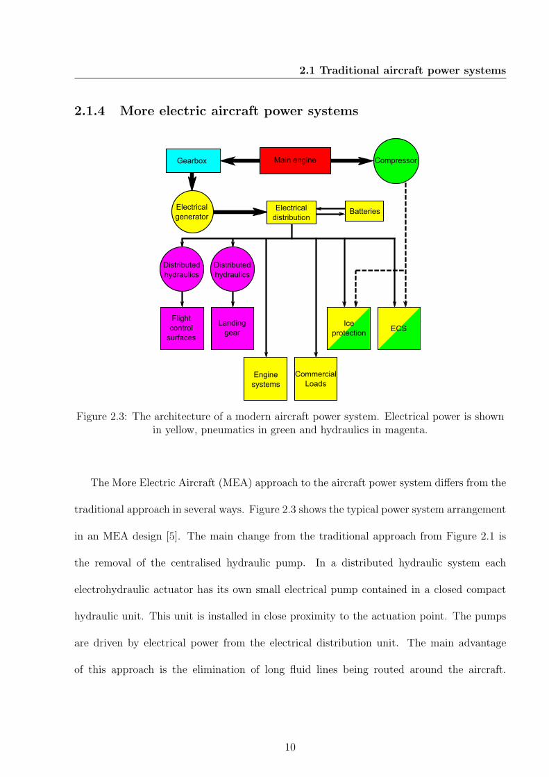
Figure 2.3: The architecture of a modern aircraft power system. Electrical power is shownin yellow, pneumatics in green and hydraulics in magenta.
The More Electric Aircraft (MEA) approach to the aircraft power system differs from the
traditional approach in several ways. Figure 2.3 shows the typical power system arrangement
in an MEA design [5]. The main change from the traditional approach from Figure 2.1 is
the removal of the centralised hydraulic pump. In a distributed hydraulic system each
electrohydraulic actuator has its own small electrical pump contained in a closed compact
hydraulic unit. This unit is installed in close proximity to the actuation point. The pumps
are driven by electrical power from the electrical distribution unit. The main advantage
of this approach is the elimination of long fluid lines being routed around the aircraft.
10

2.1 Traditional aircraft power systems
Although there is no meaningful saving in mass by adopting this approach, the maintenance
benefit is great. The hydraulic units can be individually removed and replaced with only
electrical and control cables required to be detached. The other main difference is that
the pneumatic system has been relegated to being purely a back up with the ECS and ice
protection now running on electrical power. For the ice protection this involves a complete
change in philosophy. Instead of using a warm stream of air from the engine to prevent
ice forming, electric heaters, similar to those used for many years in the rear windscreens
of cars, are used. These heat the control surfaces, inlet cowls and windscreen to prevent
ice forming. The major advantage of this system is that there are no longer ducts which
can become blocked. The disadvantage is that the electrical power demand is considerably
greater. Ultimately the aim is to completely eliminate the hydraulics from this system and
replace them with electrical only actuation. This approach is shown in Figure 2.4.
Electrical actuators use the same philosophy as the distributed hydraulic actuators. They
eliminate the need for a centralised pump and long fluid lines. Electrical actuation has been
used in model radio controlled aircraft for some time, however it has proved difficult to scale
up for full sized commercial aircraft. This is primarily due to the safety requirements placed
on commercial aircraft systems. For the flaps this is fewer than 10−9 failures per flight hour of
operation. Electric motors have failure rates of around 10−5 per flight hour of operation [6].
However research and development is continuing to pursue this option with current methods
including highly geared three-phase electric motors offering comparable shaft torque and
actuation time to electrohydraulic systems.
11

2.2 MEA electrical power system
Main engine
Flight
control
surfaces
Landing
gear
Engine
systems
Commercial
Loads
Ice
protectionECS
Gearbox
Electrical
generatorBatteriesElectrical
distribution
Electrical
actuator
Electrical
actuator
Compressor
Figure 2.4: The architecture of a more electric aircraft power system. Electrical power isshown in yellow, pneumatics in green and hydraulics in magenta.
2.2 MEA electrical power system
The electrical power distribution system of a MEA is described in this section and is illus-
trated in Figure 2.5. First we look at the difference between primary and secondary power.
Next the need for energy storage and its methods are introduced. Finally, methods of power
distribution will be considered. Each engine on an aircraft feeds a generator. However, for
the sake of brevity, the electrical generator of the aircraft EPS is not considered in this thesis
as the focus of this work is on power distribution.
12

2.2 MEA electrical power system
Electrical
generator
Electrical
generator
Primary Primary
Secondary Secondary Secondary
Generation
Distribution
Loads
Umbilical
Low power Low power Low power
High Power
Figure 2.5: Block diagram of the electrical power system of an aircraft showing:generators; primary and secondary power distribution; and loads
2.2.1 Primary power
Primary power refers to the first level of power distribution in the electrical power system
after the generators [7]. This is the highest power level in an aircraft. The Boeing 767
passenger aircraft has two engine-driven 90 kV A generators. This provides 115 − 200 V
400 Hz three-phase AC power for the aircraft [2]. The high frequency allows tansformers
and inductors to be smaller and lighter saving a significant amount of mass. Primary power
distribution deals with currents in the order of 100 A. Several primary power distribution
systems are directly connected to the electrical generators on the engines. The loads of the
primary power system include:
• The primary power system itself in the form of redundant back ups. This means
13

2.2 MEA electrical power system
the EPS has the ability to reroute power in the event of a generator failure. This is
represented by the umbilical connection between the primary power distribution blocks
in Figure 2.5.
• The highest power loads. This is likely to include electrical de-icing systems and
hydraulic pump drives.
• The secondary power distribution system.
2.2.2 Secondary power
Secondary power is the level of power distribution below primary power. The loads sup-
plied by the secondary power system include the avionics, lighting, ECS and others. The
secondary loads are of a lower power than the primary loads, typically tens of Amps. The
secondary power distribution system has in built protection circuits which prevent problems
propagating back to the primary power distribution system.
2.2.3 Energy storage
An aircraft cannot normally adapt power generation dynamically to meet the variation in
demand of the electrical power systems. The electrical energy is generated through a gearbox
by the rotary part of the engines. The primary purpose of the engines is to maintain smooth,
safe flight. Engine power cannot be stepped up and down simply to meet the electrical
demands of the power system. Clearly the electrical power system must feature energy
storage in order to supplement fluctuations in the electrical power demand. Although there
14

2.2 MEA electrical power system
are many technologies for storing energy in electrical power systems, lithium-ion batteries
are the most widely used due to their high energy density and flexible form [8]. Although the
batteries could be contained in a single location, on large passenger aircraft from a design
point of view it is more favourable to distribute them. This has many benefits for mass
distribution and centre of gravity (CoG) requirements. It also creates spacial redundancy in
the power system as individual battery failures will effect fewer cells. The move towards MEA
will require larger amounts of electrical energy storage to supplement the ever increasing
demand. This can be provided by increasing the number of battery cells used to store
energy in the EPS. However, this presents problems for the energy distribution system as a
whole.
2.2.4 Power switches
CoilControl
input
High
current
terminal
High
current
terminal
Spring
Armature
Figure 2.6: A schematic representation of an electromechanical relay with a photograph forcomparison [9]. The relay occupies a space envelope of 98× 44× 87 mm and weighs
approximately 570 g.
Both the primary and secondary power distribution systems consist of many power
switches. These are used to route power to the loads and disconnect faulty systems so
failures do not propagate. In traditional aircraft the role of the power switch is filled by the
15

2.2 MEA electrical power system
electromechanical relay. Electromechanical relays are electrically driven mechanical switches.
Figure 2.6 shows a typical high current relay. Metal contacts are separated by a sprung ar-
mature which is closed by passing a current through an electromagnetic coil. The main
advantage of the electromechanical relay is the ultra low conduction resistance. When the
switch is closed it has virtually zero resistance forming a near perfect conductor. However,
there are some significant drawbacks from using an electromechanical switch. The first is
the size and mass of the switch. The magnetic coils required to actuate the switch are large
and heavy. Secondly, although the switches have negligible losses on the contact side, the
coil side needs constant power in order to function. This reduces the overall energy effi-
ciency of the system. Thirdly, electromechanical relays do not switch cleanly and suffer from
contact bouncing. This bouncing of the contacts can cause several large voltage spikes in
the presence of stray inductance due to the high resulting di/dt. These spikes need to be
suppressed through the use of snubbers which adds to the mass and volume of the system.
Finally, the switching speed of electromechanical relays is pedestrian when compared with
equivalent semiconductor switches. It is also is very slow to respond when considered in the
context of the change in current or voltage conditions in a high power electrical circuit with
large amounts of energy stored in low impedance sources, such as lithium-ion batteries. This
is important because of the need for, and limitations of, fault detection.
2.2.5 Fault detection
It is important that the electrical distribution system is able to take action if a fault is
detected in one of the loads. The most stressful faults for the power distribution system
16

2.2 MEA electrical power system
are those that involve sudden and dramatic increases in energy. These faults, although
extremely rare, result in very high power dissipation in the power distribution system. If they
are not properly managed they can result in significant damage to the power switches but
also, more significantly, the high power wiring that runs throughout the aircraft. Damage
to the power distribution units, while undesirable, does not require complex repair work.
Power distribution boards take the form of self contained units which can be removed and
replaced with relative ease. The electrical cables however require significant effort to repair
or replace as they are distributed widely across the aircraft. The complication in this is
that not every power surge is the result of a fault. Parasitic and fixed capacitances in the
electrical loads can result in fast high energy transients. The fault detection system in an
electrical distribution unit must allow these short transients to pass so that load operation
can continue uninterrupted. However it must also be capable of distinguishing a true fault
and taking action. This means that a finite ‘fault detection time’ is introduced, any fault
will continue for at least this length of time before the switch is opened and the circuit is
broken. The combination of the time required to detect a fault and the time taken for the
electromechanical relay to open to break the circuit is significant. It is more significant in
the MEA because of the batteries. MEA require larger battery packs to cope with the higher
electrical demand. Currently, the most cost effective solution in terms of mass and volume is
the lithium-ion battery [8]. Lithium-ion batteries have exceedingly low internal impedance.
This means that in a short circuit condition they can deliver effectively limitless current.
The current is only effectively limitless because sustained rapid discharge causes the battery
cells to quickly heat up and vent, destroying themselves and their surroundings. One of the
17

2.2 MEA electrical power system
major drawbacks of an electromechanical relay is that if it fails during a surge condition it
fails closed, maintaining the short circuit. This is due to the contacts welding shut from
the extreme high temperatures generated by the high current during the surge. To prevent
this type of failure, the relay must have a considerably higher rating than that required for
normal operation. This adds considerable mass to the switch as the armature and contact
area must be increased to meet the higher current demand. In addition, the higher current
rating of the switch requires a larger coil to close it. This slows down the switching speed of
the relay, exacerbating the problem.
2.2.6 The solution
The answer to the question of what can be done in light of this problem appears to be simple
simple. Replace the electromechanical relay with a power semiconductor switch, a power
transistor. However, there are a wide variety of power semiconductor switches available.
Figure 1.1 shows how the various devices relate to each other in terms of switching speed
and equivalent power capacity. Each has its own unique properties making it suitable or
unsuitable for this application. The voltage and current range seen by the switch under
normal operation will be 400 V , 10 A (based on 200 V AC [2]). However the surge current
could be up to ten times this (100 A) and the safety overhead for the voltage limit must
be at least two times the peak to peak line voltage. Therefore a 1000 V 100 A switch is
required for this application. This effectively narrows the field of possible transistors to four
families. They are:
• The Silicon Power MOSFET
18

2.2 MEA electrical power system
• The Silicon Superjunction Power MOSFET
• The Silicon Carbide Power MOSFET
• The Silicon IGBT
Each of these devices will be considered in detail in Chapter 3. Thyristors are not
suitable as they are latching devices and therefore cannot be turned off during conduction.
Gate turn-off thyristors (GTO) and Insulated Gate Commutated Thyristors (IGCT)are not
considered as they are more suited to much higher voltages and exhibit a relatively high
forward voltage drop which would lead to increased conduction losses especially at lower
currents. The IGBT has made the power bipolar junction transistor (BJT) redundant in
all but the highest volume, lowest cost applications [4]. The extent to which the IGBT has
superseded the BJT is so great that the BJT is not included in Figure 1.1. Silicon carbide
junction gate field-effect transistors (JFET) are not considered, as only normally on devices
are currently available. This would cause problems making the distribution failure tolerant
as a failure of the switch control system would leave the device permanently on. Gallium
nitride (GaN) and gallium arsenide (GaAs) high electron mobility transistors (HEMT) are
also not considered as they are not widely commercially available and, due to their lateral
construction, difficult to scale up to higher voltages and currents. HEMTs are considerably
better suited to high frequency, low power density applications.
19

2.3 Summary
2.3 Summary
In summary, traditional aircraft use a variety of methods to power their systems. These
include hydraulics, pneumatics and power electronics. The future of aircraft development
known as the More Electric Aircraft calls for a reduction in traditional hydraulic and pneu-
matic systems in favour of more electrical systems. This approach is designed to reduce
complexity and maintenance costs without impacting the mass of the systems and without
compromising on safety. One of the hurdles that must be overcome is what to replace the
current power switch technology with. The power switches in traditional aircraft are elec-
tromechanical relays. However these switches are not suitable for scaling in order to meet
the higher power demands of the More Electric Aircraft. This is largely due to their slow
switching speed which renders them unable to cope with the potential high energy current
surges associated with large lithium-ion batteries and short circuits. The solution is to re-
place the relay with a power semiconductor switch. The choices of switch and a discussion
of which is the most suitable option is found in Chapter 3.
20

Chapter
3 Semiconductor switches
In this chapter the characteristics of four semiconductor devices identified in the previous
chapter will be discussed. The silicon power MOSFET, the silicon superjunction MOSFET,
the silicon IGBT and the silicon carbide power MOSFET. First the characteristics of an
ideal switch will be outlined, then the four devices will be described. For each device the
theory of its operation will be discussed. The structure will be shown along with details of
their forward characteristics. Switching performance will be covered and the pros and cons
of each device will be summarised. Finally, the fabrication steps required to manufacture
each device will also be summarised. Also in this chapter a few of the more novel variations
of these standard devices will be described. Finally, a new device called the HUBFET will
be proposed.
21

3.1 The ideal switch
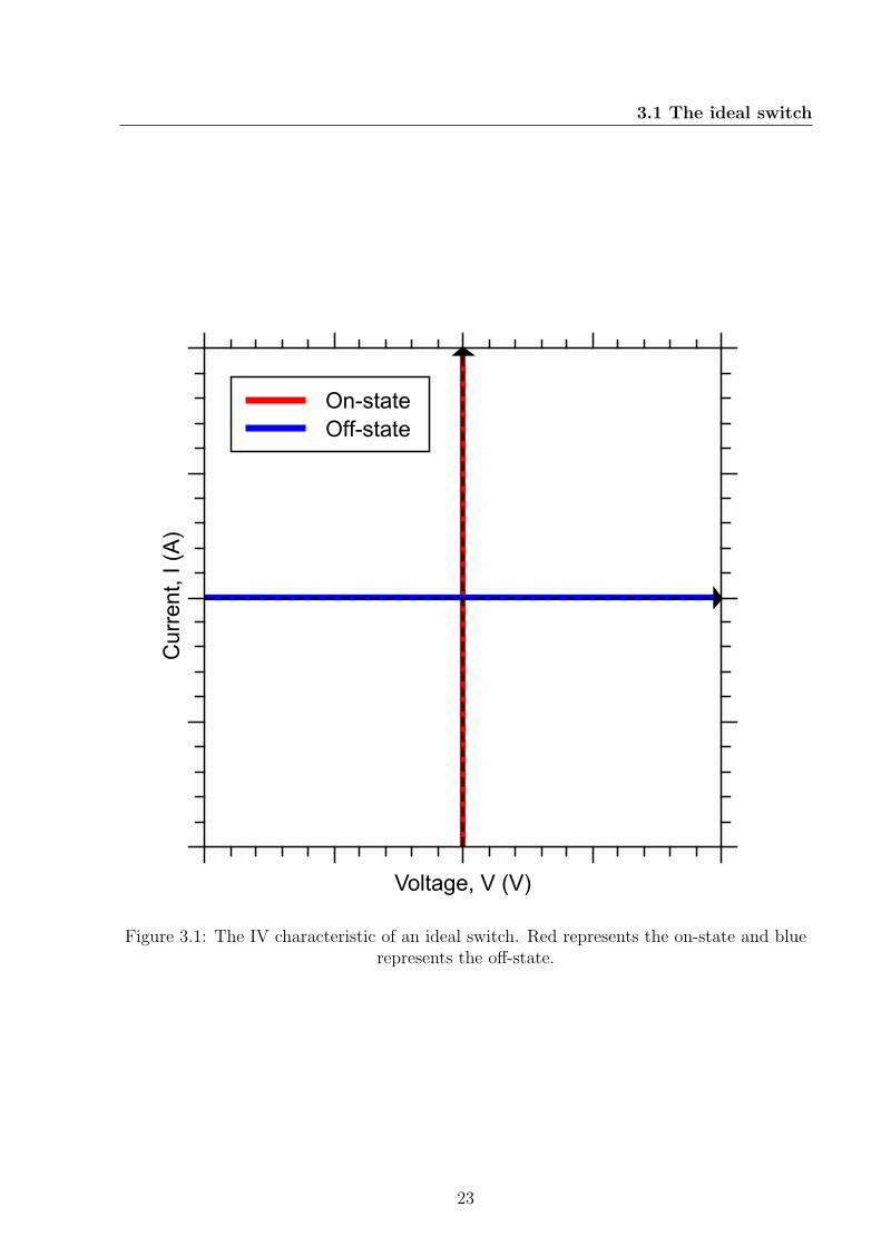
3.1 The ideal switch
The characteristics of an ideal switch are shown in Figure 3.1 [10]. An ideal switch can
block an infinite voltage in the off-state and conduct with zero resistance in the on-state.
Depending on the application it may be desirable for the switch to conduct in both directions
in the on-state or to commutate current under reverse bias. This is the case in inductive
switching applications such as inverters and rectifiers in motor drives. In reality no device
will exhibit the ideal characteristics. All semiconductor switches have a finite breakdown
voltage and a limit to forward conduction that results in some energy being lost as heat. An
ideal switch will transition from the on-state to the off-state, and vice versa, instantaneously.
Again, this is not actually possible. The finite switching time of real devices also leads to
power losses. These are referred to as switching losses.
22
3.1 The ideal switch
Current, I (A)
Voltage, V (V)
On-state
Off-state
Figure 3.1: The IV characteristic of an ideal switch. Red represents the on-state and bluerepresents the off-state.
23

3.2 The vertical power MOSFET
3.2 The vertical power MOSFET
3.2.1 History
The Metal-Oxide-Semiconductor Field Effect Transistor (MOSFET) is a simple semiconduc-
tor switch. Although the concept was patented in 1926 by Lillienfield and in 1934 by Heil, it
was first demonstrated at Bell Labs by Kahng and Atalla in 1959 [11]. It is structurally differ-
ent to its predecessor, the BJT, as the control terminal is electrically insulated from the rest
of the device. This insulator is traditionally a native oxide between the metal contact and the
semiconductor material, hence the name Metal-Oxide-Semiconductor (MOS). Initially the
MOSFET was used in integrated circuits (IC) with industry driving for higher numbers of
smaller switches on each IC. In the 1970’s and 1980’s the idea of the power MOSFET began
to emerge. Moving from lateral to vertical devices allowed the power MOSFET to sustain
higher breakdown voltages and high current densities. Previous lateral designs were limited
to high voltage or high current but not both. From the mid 1980’s until recently the most
common power MOSFET was the vertical diffused MOS (VDMOS) or double diffused MOS
(DMOS). More recently exotic structures have been developed such as the trench gate and
the superjunction. However the VDMOS still dominates the market and is the device that
will be described here. The vertical power MOSFET is utilised over a wide range of voltages,
from 10 V − 1000 V . Above 400 V it is usually more efficient to use an IGBT due to the
increasing power loss arising from the MOSFETs wide drift region and unipolar conduction.
It is only usually in specific applications, that require rapid switching, that MOSFET will
be used instead of an IGBT above 400 V . Silicon MOSFETs are not commercially available
24
3.2 The vertical power MOSFET
at blocking voltages of over 1.2 kV
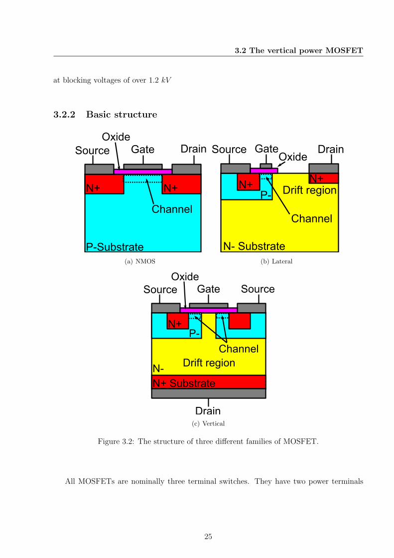
3.2.2 Basic structure
N+ N+
P-Substrate
Oxide
Channel
GateSource Drain
(a) NMOS
N+P-
Oxide
N- Substrate
N+
Channel
Source Gate Drain
Drift region
(b) Lateral
Oxide
N+ Substrate
N+P-
N-
Channel
Drain
GateSource Source
Drift region
(c) Vertical
Figure 3.2: The structure of three different families of MOSFET.
All MOSFETs are nominally three terminal switches. They have two power terminals
25

3.2 The vertical power MOSFET
known as source and drain and a control terminal known as the gate. MOSFETs are unipo-
lar devices meaning current flow only comes from one type of charge carrier. During forward
conduction the charge carriers flow from the source to the drain. Figure 3.2 shows the ba-
sic structure of a simple NMOS MOSFET, a lateral power MOSFET and a vertical power
MOSFET. All three devices share the same basic form of a low doped P-type region separat-
ing a pair of N-type regions. The N-type regions are at the power terminals. On the surface
above the P-type region is a layer of insulator, usually silicon dioxide (SiO2), electrically
separating the semiconductor from the metal gate contact. The insulator prevents current
from flowing through the gate into the semiconductor which reduces the energy required at
the gate to turn the device on and off to effectively zero. The switching of the MOSFET is
controlled by generating an electric field in the surface of the P-type region under the gate
contact. The NMOS switch, shown in Figure 3.2(a), is the simplest device and is the most
similar to early devices. The lateral power MOSFET, in Figure 3.2(b), takes the basic struc-
ture of the NMOS MOSFET and adds a low doped N- drift region between the source and the
drain. This drift region enables the device to block high voltages in the off state. The wider
the drift region, the higher the breakdown voltage of the device. However, in MOS devices it
is the channel which defines the maximum current that can flow during on-state conduction.
In lateral MOSFETs a wide drift region means that the maximum area available for the
channel is compromised. The vertical power MOSFET, shown in Figure 3.2(c), solves this
problem by moving the drain contact from the topside of the device to the backside. This
allows the gate-source structures, and therefore the channel, to be more densely packed on
the top side, while the drift region is extended down without either parameter compromising
26

3.2 The vertical power MOSFET
the other. In each of the structures in Figure 3.2 the channel is formed in a lightly doped
P- region. Counter-intuitively these MOSFETs are therefore known as n-channel devices.
The reason for this will be discussed in Section 3.2.3. In addition to the n-channel devices
there are also p-channel devices. P-channel power MOSFETs are not as widely used as their
n-channel equivalents as they have a higher on-state resistance. However, in applications
where reducing component count to improve reliability is a more pressing factor that con-
duction efficiency, P-channel power MOSFETs are still used to eliminate the need for charge
pumping and bootstrapping circuits in high side drive systems. this is typically in aviation
and space applications. Structurally P-channel devices are identical to the n-channel devices
with only the doping reversed, N becomes P and P becomes N. For the purpose of this
work, and for the sake of brevity, all devices referred to from here will be n- channel unless
otherwise stated.
3.2.3 Operation
The forward operation of a MOSFET is defined by the operation of the channel. During
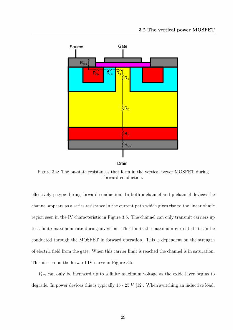
forward conduction the current path is made up of the channel and a series of resistive
elements including: the contact resistances (RCS, RCD); the N+ source resistance (RN+);
the channel resistance (Rch); the accumulation resistance (RA); the JFET resistance (RJ);
the drift region resistance (RD); and the substrate resistance (RS). These are shown in
Equation 3.1 and Figure 3.4.
RDS(on) = RCS +RCD +RN+ +Rch +RA +RJ +RD +RS (3.1)
27
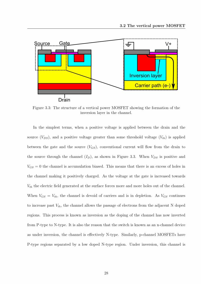
3.2 The vertical power MOSFET
Drain
GateSource V+
Inversion layer
Carrier path (e-)
Figure 3.3: The structure of a vertical power MOSFET showing the formation of theinversion layer in the channel.
In the simplest terms, when a positive voltage is applied between the drain and the
source (VDS), and a positive voltage greater than some threshold voltage (Vth) is applied
between the gate and the source (VGS), conventional current will flow from the drain to
the source through the channel (ID), as shown in Figure 3.3. When VDS is positive and
VGS = 0 the channel is accumulation biased. This means that there is an excess of holes in
the channel making it positively charged. As the voltage at the gate is increased towards
Vth the electric field generated at the surface forces more and more holes out of the channel.
When VGS = Vth, the channel is devoid of carriers and is in depletion. As VGS continues
to increase past Vth, the channel allows the passage of electrons from the adjacent N doped
regions. This process is known as inversion as the doping of the channel has now inverted
from P-type to N-type. It is also the reason that the switch is known as an n-channel device
as under inversion, the channel is effectively N-type. Similarly, p-channel MOSFETs have
P-type regions separated by a low doped N-type region. Under inversion, this channel is
28
3.2 The vertical power MOSFET
Drain
GateSource
RCS
RN+ Rch RA
RJ
RD
RS
RCD
Figure 3.4: The on-state resistances that form in the vertical power MOSFET duringforward conduction.
effectively p-type during forward conduction. In both n-channel and p-channel devices the
channel appears as a series resistance in the current path which gives rise to the linear ohmic
region seen in the IV characteristic in Figure 3.5. The channel can only transmit carriers up
to a finite maximum rate during inversion. This limits the maximum current that can be
conducted through the MOSFET in forward operation. This is dependent on the strength
of electric field from the gate. When this carrier limit is reached the channel is in saturation.
This is seen on the forward IV curve in Figure 3.5.
VGS can only be increased up to a finite maximum voltage as the oxide layer begins to
degrade. In power devices this is typically 15 - 25 V [12]. When switching an inductive load,
29

3.2 The vertical power MOSFET
the switching waveforms of a power MOSFET look like those shown in Figure 3.7.
VGG (green) is the digital control signal sent to the gate of the MOSFET. VGS (yellow)
is the actual voltage seen between the gate and the source. This voltage is non-linear due to
the various parasitic miller capacitances the exist within the gate structure of the MOSFET.
To turn the MOSFET on, a control signal is sent to the gate. When VGS has risen above
the threshold voltage required for channel inversion, the current through the device (ID,
magenta) rises. Then the voltage across the switch (VDS, cyan) falls. During this period
it can be seen that for a short length of time there is a high current flowing through the
MOSFET and a high voltage between the power terminals. This overlap represents a large
instantaneous power loss known as the turn-on loss. When the device is turned off, the
process is similar. VGS falls, VDS rises and ID falls. Again there is an overlap where both
high voltage and high current are present. This period represents the turn-off loss. There
is also a slight voltage overshoot during turn-off due to stary inductance. This is essential
to turn on the freewheel diode in the circuit as seen in Figure 3.6. The magnitude of the
overshoot is dependent on the stray inductance in the circuit. If this inductance is high
then the overshoot is also high. If the stray inductance is low, then the overshoot is also
low. It is doubly important to minimise this overshoot during inductive switching. Firstly,
because it occurs at time when the drain current is also very high, maximising its impact.
It is also important to minimise the overshoot because it is possible for the spike to exceed
the breakdown voltage of the MOSFET leading to avalanche breakdown.
One particularly important property of any power MOSFET is its ability to block forward
voltage in the off-state. Planar CMOS devices are only required to block a few volts which
30

3.2 The vertical power MOSFET
can be supported by the p-type region between the drain and the source. However some
power MOSFETs must be capable of blocking over 1000 V so another region must be added
to the device. This region is the lightly doped N- drift region between the P-type channel
and the drain. The maximum blocking voltage a power semiconductor switch can sustain is
limited by a phenomenon known as avalanche breakdown. In a power MOSFET increasing
VDS creates a depletion region between the source and the drain. This effectively prevents
current from flowing between the terminals as carriers cannot enter the depletion region.
However, due to phenomenon such as space-charge generation and diffusion from adjacent
quasi-neutral regions, some carriers do end up in the drift region and are rapidly accelerated
across by the electric field [4]. The small current arising from this is known as leakage current.
As the electric field strength increases and the voltage across the terminals approaches the
breakdown voltage these carriers gain enough kinetic energy to knock electrons out of the
lattice in a process known as impact ionisation. The newly generated electrons are also
accelerated by the electric field and they themselves generate further carriers. This process
rapidly floods the drift region with carriers and the MOSFET becomes a conductor. This
multiplicative process of carrier generation leading to uncontrolled conduction is known as
avalanche breakdown and can only be stopped by reducing VDS [4]. The breakdown voltage
of a MOSFET can be increased by introducing a lightly doped drift region between the
channel and the drain contact. Lighter doping leads to a higher breakdown voltage but also
a higher conduction resistance. Similarly, a wider drift region results in a higher breakdown
voltage but also a higher conduction resistance. The optimum drift region width and doping
concentration for a given breakdown voltage in silicon (ie. Results in the lowest on-state
31

3.2 The vertical power MOSFET
resistance) is given by Equations 3.2 and 3.3 [4].
VBR = 5.34× 10¹³N−3/4D (3.2)
Wpp = 2.67× 10¹⁰N−7/8D (3.3)
Where VBR is the breakdown voltage (V ), Wpp is the drift region width (cm) and ND is
the doping concentration (atoms.cm−3). The breakdown voltage of a lateral power MOSFET
can be increased by introducing a lightly doped drift region between the channel and the
drain contact. However, the current is limited by the saturation current in the channel. The
current can be increased by increasing the channel area but this leads to devices taking up
a large amount of silicon area. It is considerably more common to use the vertical power
MOSFET structure when fabricating high voltage power MOSFETs. Here, the drain contact
is relocated to the backside of the wafer and the drift region is extended vertically to give
higher breakdown voltages. This allows the topside of the wafer to be fully utilised for gate
area which increases the current capacity of the device for a given silicon area (specific current
density, J (I.cm−2)). Equations 3.2 and 3.3 can be used to plot a graph showing the unipolar
limit of silicon in vertical devices. This is the relationship between breakdown voltage and
specific on-state resistance. In power MOSFETs and other unipolar devices required to block
over 100 V , the largest component of the forward on-state resistance is the resistance of the
drift region. Therefore the silicon limit graph can be used to approximate the minimum
specific on-state resistance for a MOSFET for any given breakdown voltage. The unipolar
limit is a useful tool for comparing power semiconductor devices of different materials, as will
32

3.2 The vertical power MOSFET
be seen later in this chapter. One feature of both the lateral and vertical power MOSFET is
the integration of a PiN antiparallel diode known as the body diode. This diode is present
in the structure because of the need to suppress another parasitic component that emerges
when a MOSFET is fabricated, the parasitic BJT. In n-channel power MOSFETs an NPN
bipolar junction transistor is formed from the N+ source region, the P-base and the N- drift
region. If this transistor turns on then the MOSFET will conduct independently of the gate
control which, it is safe to say, is undesirable. To ensure that this cannot happen the P-base
is electrically shorted to the N+ source by the source metal contact. This ties the BJT base
and collector terminals together permanently, meaning the BJT can never turn on. This
shorting also means that the source and drain contacts are joined by a PiN structure which
forms the afore mentioned diode. The diode characteristic can clearly be seen in the third
quadrant of the MOSFET IV curve in Figure 3.5. The body diode proves useful when power
MOSFETs are used as part of a bridge circuit in inductive switching applications. In these
types of applications the body diode can be used to commutate current through the inductor
allowing a smooth flow of power around the circuit.
3.2.4 Fabrication
Vertical power MOSFETs are fabricated on highly doped silicon wafers. This bulk wafer is
a thick ( 250 µm) highly doped (1 × 10¹⁹ - 1 × 1020 cm−3) wafer. The thickness provides
mechanical rigidity during production and the high doping concentration means it exhibits
metal like conduction with negligible resistance. The wafer also serves as a uniform single
crystal starting point for epitaxial growth. On top of the bulk wafer the drift region is grown
33

3.2 The vertical power MOSFET
as an epitaxial layer using a process of chemical vapour deposition (CVD). The thickness
and doping of this layer is chosen using the drift equations 3.2 and 3.3. The N-type and
P-type regions that form the gate structure are fabricated using ion implantation, diffusion
and thermal annealing processes in the top surface, the gate oxide is grown and the metal
for the contacts is applied to the top and back sides of the wafer. It is important to note
that in Si, dopant atoms can be implanted and thermally diffused. This allows the process
of fabricating the gate structure to be more flexible as dopant atoms can diffuse laterally,
for example under the gate oxide. The fabrication process for the vertical power MOSFET
is relatively simple and well defined. The process is suitable for high volume production and
the techniques are widely used.
3.2.5 Vertical power MOSFET summary
Many aspects of the vertical power MOSFET make it a suitable device for use in a solid state
DC power controller for aircraft. However, its has limited capability for sudden high energy
short circuits. Due to its ohmic behaviour, power losses increases exponentially as current
increases linearly. The only way of increasing the high current capability of the device is
by increasing the silicon area used by the MOSFET. This will impact the compactness of
the power module which would compromise its suitability for aircraft applications as well as
increasing the cost.
34
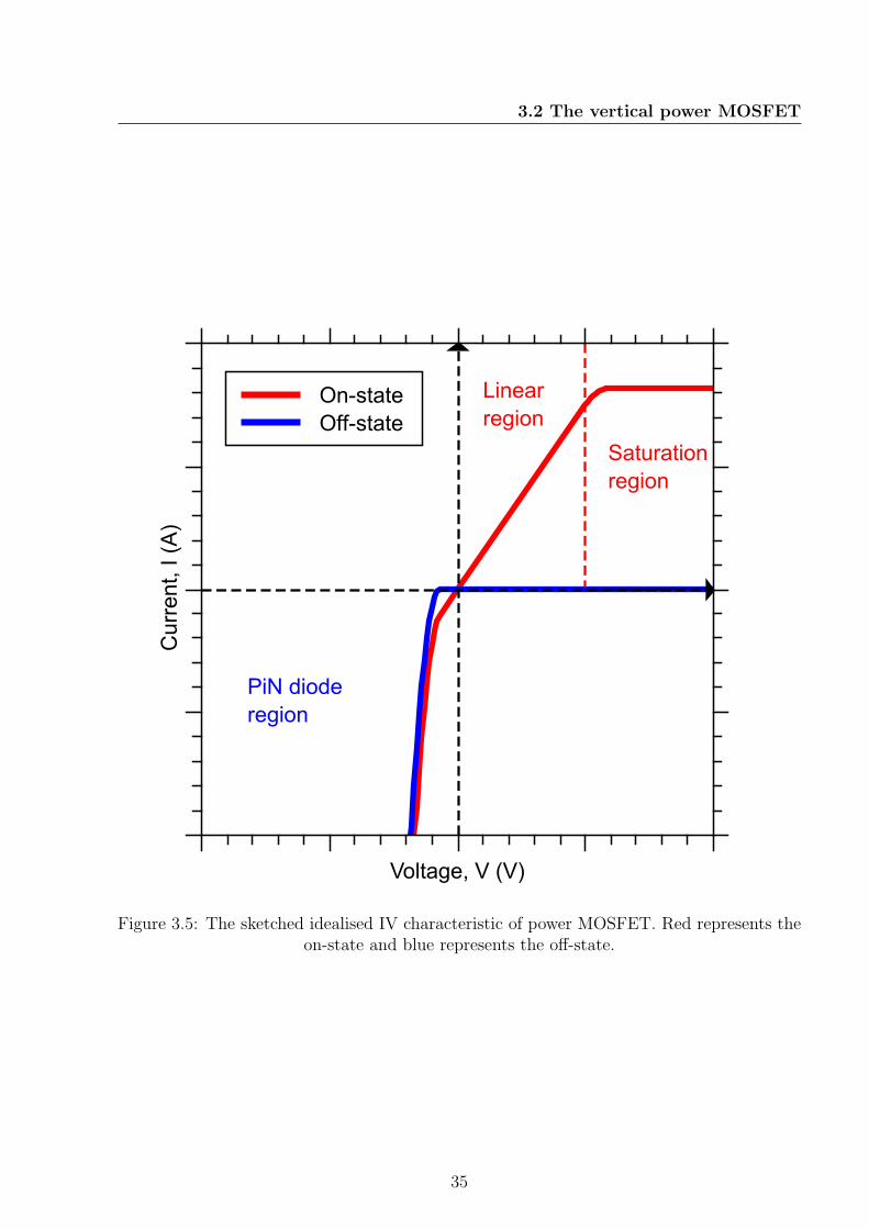
3.2 The vertical power MOSFET
Current, I (A)
Voltage, V (V)
On-state
Off-state
Saturation
region
Linear
region
PiN diode
region
Figure 3.5: The sketched idealised IV characteristic of power MOSFET. Red represents theon-state and blue represents the off-state.
35
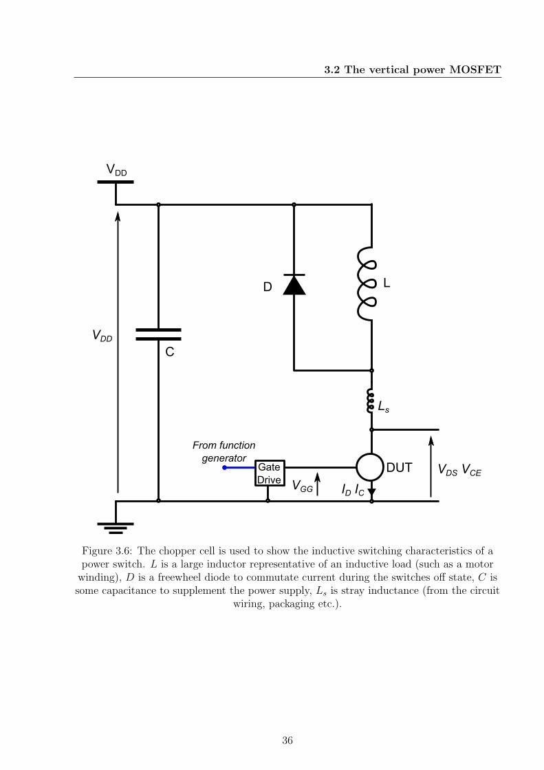
3.2 The vertical power MOSFET
C
L
DUT
D
VDD
ID IC
VDS VCE
VDD
Gate
Drive VGG
From function
generator
Ls
Figure 3.6: The chopper cell is used to show the inductive switching characteristics of apower switch. L is a large inductor representative of an inductive load (such as a motorwinding), D is a freewheel diode to commutate current during the switches off state, C issome capacitance to supplement the power supply, Ls is stray inductance (from the circuit
wiring, packaging etc.).
36
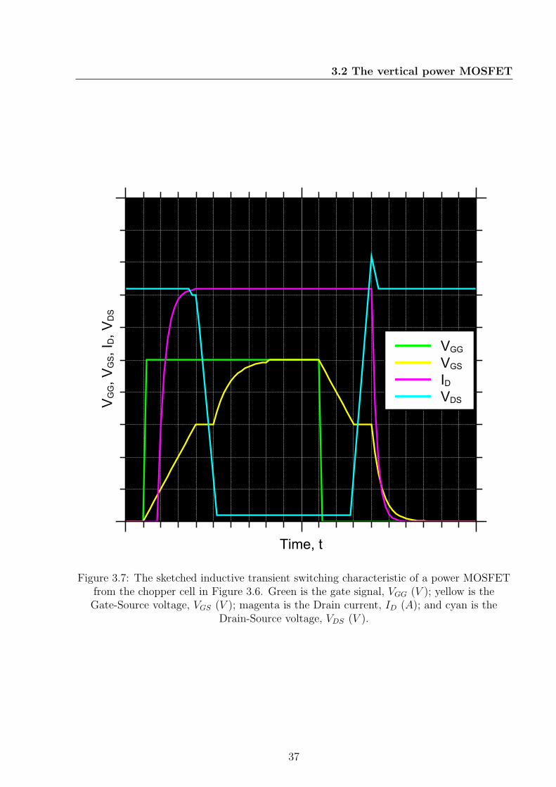
3.2 The vertical power MOSFET
VGG, VGS, I D, VDS
Time, t
VGG
VGS
ID
VDS
Figure 3.7: The sketched inductive transient switching characteristic of a power MOSFETfrom the chopper cell in Figure 3.6. Green is the gate signal, VGG (V ); yellow is theGate-Source voltage, VGS (V ); magenta is the Drain current, ID (A); and cyan is the
Drain-Source voltage, VDS (V ).
37

3.3 The superjunction MOSFET
3.3 The superjunction MOSFET
3.3.1 History
The silicon superjunction MOSFET is a relatively recent invention. The lateral SJ MOSFET
was patented in 1988 by David Coe [13], followed by other patents for vertical devices in
1993 and 1995 [14, 15]. It was first commercialised by Infineon technologies in the late 90’s,
in a device trademarked under the name CoolMOS [16,17]. Since then other companies have
developed their own versions using a similar structure such as the ST MDMesh devices [18].
The SJ MOSFET is a novel structure based on the traditional vertical power MOSFET. It
utilises the theory of charge compensation to dramatically reduce the resistivity of the drift
region. Superjunction MOSFETs are best used in applications requiring blocking voltages
of 500-800 V, fast switching and extremely low conduction loss.
3.3.2 Basic structure
The superjunction MOSFET is a vertical power MOSFET that utilises a technique known
as charge balancing or charge compensation. This technique has allowed silicon power MOS-
FETs to be developed with five times the current density of traditional MOSFETs with the
same silicon area and blocking voltage. As described in Section 3.2 the breakdown volt-
age of a power device is defined by the width and doping concentration of the drift region.
These properties affect the strength and distribution of the electric field generated when a
voltage is applied between the source and the drain contacts when the device is off. Charge
balancing allows the fabrication of devices where the drift region has a higher doping con-
38

3.3 The superjunction MOSFET
Oxide
N+ Substrate
N+P-
N
Drain
GateSource Source
Drift regionP
Figure 3.8: Structure of the vertical superjunction power MOSFET
centration, and therefore lower resistivity, whilst maintaining the same width and blocking
voltage. The technique involves fabricating additional P-type doped columns through the
drift region, as seen in Figure 3.8. In order for this technique to result in the large drop
in resistivity the following criteria must be satisfied. The doping integral along a line per-
pendicular to the current flow must remain smaller than the Silicon specific breakthrough
charge (approx 2 × 1012cm−2) [16]. This can be satisfied if the P-type columns have the
same width and doping concentration as the N-type drift region. Using this technique, the
N-type drift region doping can be increased by a factor of 10 resulting in a 10 fold drop in
resistivity. However, the area of conduction path is halved due the presence of the P-type
columns which do not conduct current. The combination of these two factors results in the
5 fold increase in current density for a SJ MOSFET with a given blocking voltage. Using
this technique, increases in blocking voltage are simply a case of extending the width of the
drift regions and the P-type columns along with them [17].
39

3.3 The superjunction MOSFET
3.3.3 Operation
The operation of a superjunction MOSFET is identical to that of a conventional vertical
power MOSFET as described in Section 3.2.3. The device has been designed such that
it can act as a like for like replacement for the conventional MOSFET. The gate voltage
parameters are the same as for conventional MOSFETs, therefore there is no need to modify
control circuitry to compensate for the new device.
3.3.4 Fabrication
Conventional vertical power MOSFETs have a drift region that is fabricated in a single
stage of epitaxial growth. The dopant impurities are present during the growth process
and form part of the lattice leading to a uniform doping profile though the whole of the
drift region. Superjunction MOSFETs are fabricated using a variety of techniques. These
include: etching deep vertical trenches into a substrate and growing thin P and N-type
epitaxial layers on the sides of the trenches to form a vertical structure of columns [19];
etching sloped trenches into a doped substrate and filling the trenches with columns of
silicon with the opposite doping [20]; and growing multiple thin epitaxial layers of undoped
silicon and implanting the columns layer by layer to form the structure. This final method
is the technique commercialised by Infineon for the CoolMOS device. Once the layers have
been grown and implanted, a diffusion anneal is performed to create the coherent columns.
Each of these methods introduces problems when scaling the devices for higher voltages. The
lateral epitaxial growth in deep trenches becomes more and more difficult as the trenches
get deeper. In the work presented by Moens et al. [19] not all of the silicon area is used
40

3.3 The superjunction MOSFET
to create the superjunction columns leading to a reduction in current density. This reduces
the effectiveness of the superjunction concept. In the method demonstrated by Takami et
al. [20] the deep trenches are sloped to allow epitaxial silicon to completely fill the trenches.
However this distorts the charge balancing structure and again reduces the benefit of of the
superjunction. Finally the multiple vertical epitaxy and implantation method used by Deboy
et al. [16] is expensive to scale up as adding additional layers to the process dramatically
increases the cost. It also becomes increasingly difficult to align all of the layers to form the
uniform pillars that are needed for a high quality SJ structure.
3.3.5 Superjunction MOSFET summary
The superjunction MOSFET is an advanced modification of the conventional vertical power
MOSFET. Its unique structure enables devices to break the unipolar silicon limit with its
record low on-state resistance. However, it is limited in its application because of its inherent
complexity. The first paper by Deboy et al from 1998 that describes the charge compen-
sated structure promises 1000 V devices in the seemingly imminent future [16]. However,
fifteen years later these devices have not been commercially realised. 650 V superjunction
MOSFETs are prevalent, however above this voltage few devices are available. This is due
to the complex fabrication steps required to build the devices. Multiple epitaxy and implan-
tation stages are expensive and time consuming. The more layers or steps in a fabrication
process, the harder it is to ensure each layer is perfectly aligned with the others. The bene-
fits of the superjunction MOSFET all stem from the critical charge compensation structure
which must be carefully constructed in order to function effectively. As the rated voltage
41

3.4 The IGBT
approaches 1000 V the SJ MOSFET comes into competition with the simpler and cheaper
IGBT. However, in the 500 - 800 V range, the SJ MOSFET is hard to beat.
3.4 The IGBT
3.4.1 History
The Insulated Gate Bipolar Transistor has a complicated history. The name and mass
commercialisation of the device can certainly be attributed to the prolific academic B. Jayant
Baliga who first published on the device in 1979 [21] whilst working for GE. However the first
recorded patent on a device exhibiting the characteristics now associated with the IGBT can
be traced to Yamagami in 1972 [22]. Unlike the simpler MOSFET, the IGBT structure can
be altered in many ways which improve certain aspects of its operation. This section will only
describe the basic principles of the IGBT and identify some of the more prevalent and useful
modifications that have arisen since its invention. The IGBT is mainly used in applications
requiring blocking voltages of up to 6 kV and fast switching such as: electric traction; hybrid
and electric vehicles; and low voltage power conversion for the grid. Traditional MOSFETs
become less useful in this voltage range as the large drift regions required to support the
high voltages leads to large on-state power losses due to their high resistance.
3.4.2 Basic structure
Although it was described as a MOS gated Thyristor by Baliga in 1979, the structure we
now identify as an IGBT is clearly shown in his letters paper of 1979 [21]. Fundamentally
42

3.4 The IGBT
Oxide
P+ Substrate (Emitter)
N+P-
N-
Collector
GateEmitter Emitter
Drift region
P
Figure 3.9: Structure of the vertical IGBT
the structure of an IGBT, shown in Figure 3.9, is nearly identical to that of a vertical power
MOSFET, shown in Figure 3.2. They both have the three terminals, however the IGBT
combines the nomenclature of the BJT for the power terminals and the MOSFET for the
control terminal. The source becomes the emitter, the drain becomes the collector but the
gate remains the gate. This is because the conduction of current through the IGBT is bipolar,
charge is carried by both electrons and holes, therefore the power terminals are named in
the same way as the power terminals in the bipolar junction transistor. Whereas the control
terminal is a MOS interface the same as the MOSFET so the terminal is named the gate.
Aside from the differently named terminals, the gate/emitter structure that forms the MOS
interface and controls the channel in the IGBT is identical, in structure and operation, to the
gate/source structure of the MOSFET. The IGBT is also divided into two types, n-channel
and p-channel, for the same reasons as the MOSFET as explained in Section 3.2.3. Again for
simplicity all devices described in this section will be n-channel unless otherwise stated. The
43

3.4 The IGBT
major difference between the MOSFET and the IGBT, the difference that fundamentally
changes the way the device conducts current, is the P+ emitter layer, confusingly located
at the collector terminal. In p-channel IGBTs, as in the MOSFET, the doping pattern is
reversed. The drift region becomes lightly doped P-type and the emitter layer highly doped
N-type. This emitter layer fundamentally alters the structure of the device. Gone is the
PiN diode seen in the power MOSFET. The IGBT is a mono-directional device and can
only conduct in the forward direction. In addition, for n-channel IGBTs, the P+ emitter
layer creates an NPNP doping structure from the emitter to the collector creating a parasitic
thyristor in the structure of the IGBT. This thyristor is suppressed, like the parasitic BJT in
the MOSFET, by shorting the N+ gate/emitter region to the P-body under the emitter. It
is further suppressed by the inclusion of a deeper highly doped P+ region under the emitter
terminal, as seen in Figure 3.9.
3.4.3 Variations
The main variations in the structure of the IGBT are punch-through (PT), seen in Fig-
ure 3.10; and non-punch-through (NPT), seen in Figure 3.10. The NPT structure is the
same as that which has been described in this section. In this structure the electric field
generated when the device is off does not extend all the way through the drift region. The
relationship between the drift region width and doping concentration follows that shown in
equations 3.2 and 3.3 from Section 3.2. The PT structure allows IGBTs to have thinner drift
regions for the same breakdown voltage. One benefit of bipolar conduction over unipolar
conduction is that the unipolar limit does not apply. Therefore the drift region can be made
44

3.4 The IGBT
Oxide
P+ Substrate (Emitter)
N+P-
N-
Collector
GateEmitter Emitter
Drift region
P
N Buffer
Figure 3.10: Structure of the vertical Punch-through IGBT
thinner with a lower doping, without compromising the rate of current that can flow during
conduction. This is due to the flood of carriers injected from the P+ emitter. In order to
achieve this PT structure an additional layer known as the field-stop or buffer layer must
be added. This is a highly doped N+ layer between the P+ emitter and the drift region.
Its function is to reduce the electric field before it punches through to the P+ emitter [4].
As well as PT and NPT there is also a Soft Punch-Through (SPT) structure which sits in
between the NPT and PT structures. In the SPT structure the buffer layer is lightly doped,
only a little higher than the drift region. This offers a good compromise between NPT and
PT.
3.4.4 Operation
The typical IV characteristics of the IGBT are shown in Figure 3.11. Although the gate
operates in the same way as the MOSFET, which is described in Section 3.2.3, the P+
45

3.4 The IGBT
emitter means conduction is very different. The addition of the P+ emitter means there is
an additional PN junction in the current path that must be overcome before current can flow
through the device. When the voltage across the IGBT is sufficient to forward bias this PN
junction, the drift region is flooded with holes and electrons and the current flow increases
exponentially. Like the MOSFET, the current will eventually saturate due to the limitations
of the conduction capability of the channel. As it is necessary for the PN junction at the
emitter to become forward biased before the IGBT will conduct, there is always some finite
voltage drop across the IGBT when it is conducting.
Although the switching control of the IGBT is the same as that found in the power
MOSFET (discussed in Section 3.2.3), due to their MOS gate control terminals, the actual
switching of the device is different, most notably during turn-off. In a MOSFET, when the
gate voltage drops below the threshold voltage and the inversion layer is removed, the current
flow in the switch reduces straight to zero. This is because no majority carriers (electrons)
are entering the drift region and no minority carriers (holes) are present. However, in an
IGBT, when the gate voltage is reduced below the threshold voltage there are still minority
carriers (holes) present in the drift region. These carriers are removed through recombination,
but the process is relatively slow. This results in the long tail seen in the turn-off current
waveform in Figure 3.12. During this current tail the voltage across the IGBT is normally
high which results in high power loss until the current reaches zero. This is what slows
the IGBT switching time compared with a MOSFET and what causes the higher switching
losses [23]. One method of speeding up for this slow recombination is through lifetime
control [23]. Lifetime control is covered in Section 3.4.5.
46

3.4 The IGBT
3.4.5 Fabrication
Traditionally IGBTs have been fabricated in the same way as power MOSFETs, but with a
different starting substrate. For an n-channel IGBT first a highly doped P+ wafer is chosen,
then the n-drift region is epitaxially grown on top. The gate structures are implanted in the
topside, the gate oxide is grown and the contacts are deposited. In addition to these processes
IGBTs normally go through a lifetime control process. As mentioned in Section 3.4.4 this
is used to reduce the current tail during turn off by speeding up the recombination process.
The most common method of lifetime control used in IGBT fabrication is electron irradiation
of the drift region. High doses of radiation (up to 16 Megarads) can reduce the turn-off time
of an IGBT from tens of microseconds to hundreds of nanoseconds [23]. Recently there has
been an industry wide move towards thin IGBTs [24–26]. Using thinner substrates to create
power devices is beneficial for several reasons. Primarily it reduces the thermal mass of the
switch, this enables it to be cooled more effectively. As well as the thermal improvements,
thinning an IGBT until it is only as thick as the drift region means the backside of the device
is exposed for processing. This has given rise to some novel new designs including the BiGT
from ABB [27–30]. However, the ultra-thin devices are very delicate and difficult to handle
which impacts the yield and cost of production.
3.4.6 IGBT summary
Like the superjunction MOSFET, the IGBT is an advanced device that is able to break
through the unipolar silicon limit. It is suited to conducting large currents and blocking
medium to high voltages. This means the IGBT would be an appropriate device to deal with
47

3.4 The IGBT
the extreme currents from short circuit failures in a solid state power controller. However
at lower currents it becomes increasingly inefficient because of the inherent voltage drop
from forward biasing the P+ emitter at the collector terminal. The IGBT does not have
an anti-parallel diode in its structure so in inductive switching applications an additional
discrete diode must be paired with each IGBT. This increases the size of the power module
which is undesirable in most cases. IGBTs also switch slower than MOSFETs, this leads to
higher switching losses. However, IGBTs can operate at higher voltages and currents without
suffering from the same multiplicative increase in power loss seen in power MOSFETs.
48
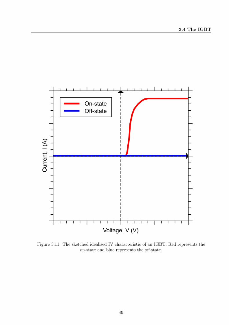
3.4 The IGBT
Current, I (A)
Voltage, V (V)
On-state
Off-state
Figure 3.11: The sketched idealised IV characteristic of an IGBT. Red represents theon-state and blue represents the off-state.
49
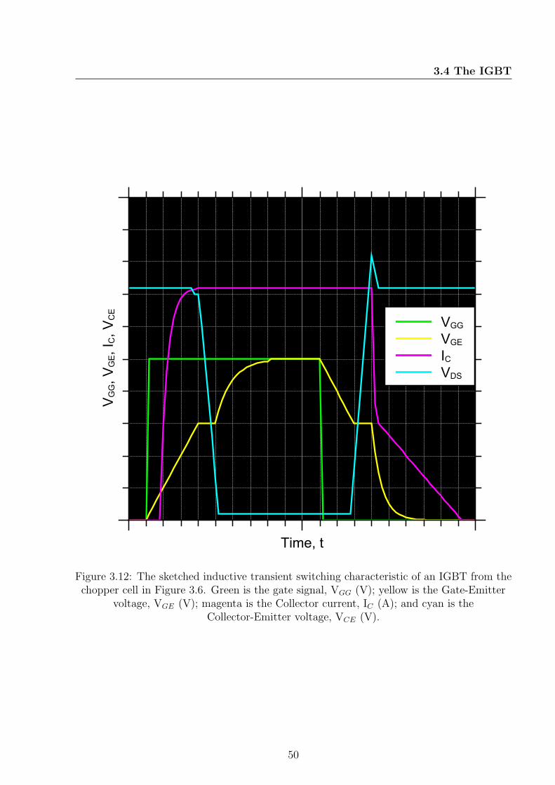
3.4 The IGBT
VGG, VGE, I C, VCE
Time, t
VGG
VGE
IC
VDS
Figure 3.12: The sketched inductive transient switching characteristic of an IGBT from thechopper cell in Figure 3.6. Green is the gate signal, VGG (V); yellow is the Gate-Emitter
voltage, VGE (V); magenta is the Collector current, IC (A); and cyan is theCollector-Emitter voltage, VCE (V).
50

3.5 The silcon carbide power MOSFET
3.5 The silcon carbide power MOSFET
3.5.1 History
The SiC MOSFET is one of the most recently developed commercially available semicon-
ductor switches. The first commercial SiC MOSFETs were made available by CREE in 2011
with the launch of their Z-FET range [31]. Before then many manufacturers and researchers
had been working on their own SiC MOSFETs, including the aforementioned Baliga [32–40].
Silicon carbide offers many potential advantages over silicon in the field of power semicon-
ductors, some of the relevant properties are shown in Table 3.1. The wide bandgap of SiC
allows higher current densities at higher voltages than Si. The wide bandgap also allows SiC
devices to operate at much higher temperatures than Si, provided the devices can be suitably
packaged. There have been many teething problems with bringing SiC MOSFETs to mar-
ket. The two most significant issues are the difficulty in creating a reliable gate oxide [41–43]
and the challenge of producing high quality monocrystalline SiC wafers [33, 44]. However,
it appears that some of these issues have been overcome as SiC MOSFETs rated at 1200 V
20 A are now commercially available. Unlike Silicon which has one crystalline polytype,
Silicon Carbide has over 250 identified polymorphs and many crystalline polytypes. Three
of these polytypes have been researched in detail for semiconductor suitability. They are 3C,
4H and 6H. The CREE Z-FET is fabricated in 4H-SiC as are other commercial SiC devices.
However, the hexagonal structure of the 4H and 6H polytypes leads to complications in
certain areas of fabrication. 3C may be able to overcome some of these issues, but obtaining
high quality mono-crystalline material in the 3C polytype is difficult [45,46].
51

3.5 The silcon carbide power MOSFET
Table 3.1: Comparison of material properties of silicon and silicon carbide [47–49].
Properties Si 3C-SiC 4H-SiC 6H-SiC
Energy Bandgap (eV) 1.10 2.36 3.23 3.0
Relative DialectricConstant
11.7 9.72 9.66 9.66
Thermal Conductivity(W/cm.K)
1.5 3.6 3.7 4.9
Density of statesConduction band(cm−3)
2.80×10¹⁹ 1.50×10¹⁹ 1.23×10¹⁹ 8.90×10¹⁹
Density of statesValence band(cm−3)
1.04×10¹⁹ 1.20×10¹⁹ 4.58×10¹⁸ 2.50×10¹⁹
3.5.2 Basic structure
The basic structure of the silicon carbide MOSFET is identical to that of a Si MOSFET,
shown in Figure 3.2. However some of the material differences between Si and SiC affect
how the structures are optimised. The main difference between Si and SiC from a device
fabrication perspective is the width of the drift region required to support the same voltage.
The wider energy bandgap of SiC (2.3 − 3.3 eV depending on polytype) compared with
silicon (1.1 eV ) allows a thinner drift region to support the same voltage whilst maintaining
the same current density. This also makes lateral devices more practical at higher current
densities as the problem mentioned in Section 3.2 of requiring wide spacing between gate
structures is partially overcome. However, the problem is simply scaled rather than being
completely eliminated. The lack of thermal dopant diffusion also prevents the self alignment
52

3.5 The silcon carbide power MOSFET
of structures. This is a key element of the fabrication of Silicon DMOS devices. In order to
fabricate a device without the benefit of diffusion, many more masking layers are required,
as all doping profiles must be created purely through implantation.
3.5.3 Operation
The operation of the SiC MOSFET is nearly identical to that of a Si MOSFET, as described
in Section 3.2.3. They have the same linear and saturation regions in the on-state, the same
body diode characteristics and the same unipolar switching characteristics. However, the
SiC MOSFET switches faster and has considerably lower on-state resistance for the same
blocking voltage and device area. The SiC MOSFET is not completely identical to the Si
MOSFET in terms of the primary source of its on-state characteristics. In the Si MOSFET
the majority of the resistance in the linear region of the on-state characteristic is from the
resistance of the drift region, as seen in Figure 3.4 and Equation 3.1. In SiC MOSFETs,
the majority of the on-state resistance is from the channel resistance. This is because the
mobility of carriers in the channel of a SiC device is very low. This is due to the number
of defects or ‘interface traps’ that form under the gate oxide in the channel. In silicon the
number of traps found in this region is negligible. In SiC, however, the density of traps is
high which has an adverse effect on channel mobility (800 cm2/(V.s) in Si compared with
20 − 60 cm2/(V.s) in SiC [50–52]). New techniques are being investigated in order to
reduce this trap density including growing SiO2 at extremely high temperatures (1500 oC)
in order to remove carbon atoms from the channel. Despite this very low channel mobility,
the reduced resistivity of the drift region more than compensates for the increased channel
53

3.5 The silcon carbide power MOSFET
resistance. This gives SiC MOSFETs considerably lower overall on-state resistances (80 mΩ
for CREE 1200 V 33 A [31]) than Si MOSFETs (400 mΩ for IXYS 1000 V 30 A [53]). The
fast switching of the SiC device increases the adverse effects of stray inductance [54, 55].
The rapid di/dt of a hard switching SiC MOSFET means that the voltage overshoot during
switching and the ringing effect after switching are greatly increased. These effects can be
severe enough to all but cancel out the reduction in switching loss that can be attributed to
the faster switching. To compensate for these problems new ultra-low inductance packaging
must be developed.
3.5.4 Fabrication
The fabrication of SiC MOSFETs must start with high quality single crystal material. This
represents the first problem. Unlike Si, SiC does not have an easily producible liquid form.
This coupled with the many polytypes of the material result in an arduous and expensive
wafer production process. The most commonly available crystalline form of SiC is the 4H
polytype. CREE sell ‘defect free’ 100 mm device grade 4H-SiC wafers with an epitaxial layer
for around ₤ 3000 each (as of 2012). Equivalent Si wafers cost closer to ₤ 100. It is only in the
last few years that high quality SiC material has become available for the fabrication of power
devices. The 3C-SiC polytype also shows some promise for both material production and
device fabrication. The benefit of 3C is that, due to its cubic structure, it has the potential
to be grown on Si substrates [45]. If this process could be commercialised it may result in a
significant reduction in SiC wafer production cost. Once a high quality substrate has been
obtained, the next step is to grow a high quality epitaxial layer in which the MOSFETs
54

3.5 The silcon carbide power MOSFET
can be fabricated. This step is critical if the already expensive wafer is to produce a high
yield of devices. Defect free epitaxy is difficult to grow for a number of reasons which I
shall not list here, suffice to say it is considerably more expensive to grow epitaxial SiC
than epitaxial Si. Although the various masking, implantation and metallisation processes
are largely the same as in Si, the gate oxide growth and diffusion processes are different in
SiC [47]. The diffusion process is different because there is effectively no thermal diffusion of
dopants in SiC. This means all dopant profiles must be created from multi-stage implants.
This will involve additional implant masking layers as in the standard Si MOS process the
gate oxide is used as a mask layer as dopants can be thermally diffused under its edge, as
seen in Section 3.2.4. This means that the gate oxide can be grown relatively early in the
fabrication process before the Si has been exposed to any of the impurities or chemicals used
in later fabrication steps. This ensures a high quality SiO2/Si interface. With SiC this early
SiO2 growth is not possible. The lack of useful lateral diffusion means all implants must be
carried out prior to the oxide growth. This involves several masking steps, the application
and removal of each of which lowers the quality of the surface that must then take the oxide.
The quality of the interface between the SiO2 and the SiC is of paramount importance to the
quality an conductivity of the channel. One of the many issues in this area is the presence
of carbon atoms at the interface [41, 42]. When SiO2 is grown thermally on SiC in the
presence of oxygen, carbon atoms displaced from the lattice remain around the interface.
These carbon atoms contribute to the low channel mobility [50–52]. One possible solution to
this is to grow the oxide at extremely high temperatures (up to 1500 oC). However currently
this process is only in the early stages of research.
55

3.6 Comparison of Devices
3.5.5 SiC MOSFET summary
Silicon carbide is one of the most promising materials for high voltage Power MOSFET
fabrication. Its wide bandgap allows much thinner devices to be fabricated for the same
blocking voltage. Estimates put the potential reduction in drift region resistance at 2000
times for devices with the same blocking voltage [47]. However this scale of improvement has
not yet been realised. Silicon Carbide MOSFETs are only beginning to be commercialised
and there is little data on their long term reliability. The biggest obstacle currently facing
the development of commercial silicon carbide MOSFETs is the low quality of the SiC/SiO2
interface. A high density of interface traps lowers the mobility of the channel significantly
which greatly increases the resistivity of the device and negates many of the benefits of
using SiC. SiC is a material that is on the cusp of greatness. However, it is not yet ready to
fully replace Si switches in all applications. The many issues still faced in the fabrication of
SiC devices result both an increase in cost and a decrease in performance. These issues are
steadily being overcome, but that is a subject for another thesis (or more likely, many other
theses).
3.6 Comparison of Devices
Each of the devices discussed so far has advantages and disadvantages for use in the aircraft
power system application discussed in Chapter 2. Although all of the devices show promise
in at least one aspect of the specification they all have equally prominent disadvantages in
another. The Si Power MOSFET is a good contender for a low current switch. However,
56

3.6 Comparison of Devices
the exponential increase in power loss as current levels rise means it must be discounted as
a single solution. The superjunction MOSFET compensates for the exponential increase in
power loss as it has a much lower on-state resistance which reduces the effect by a factor of 5.
However, the complicated fabrication method required to increase the blocking voltage makes
it uneconomical and impractical to fabricate devices in the 1200 V range this application
requires. The IGBT can be fabricated at higher voltages and can handle high currents
without the same increase in power loss as seen in the Si MOSFETs. However, the voltage
drop required to forward bias the P+ emitter leads to larger power losses at low currents. As
the majority, if not all, of the operation of the switch will be at these low currents, this would
lead to higher losses than would be desirable. Although the SiC MOSFET may solve all of
these problems, it can operate at high voltages with low losses at both high and low currents
it is not yet a fully realised commercial device. Although there are devices currently for sale,
not enough data is available on their long term reliability to enable a fully informed decision
as to their suitability for this application. There is also the issue of cost. SiC MOSFETs are
more than ten times as expensive as the superjunction MOSFETs, five times as expensive as
IGBTs and more than twice the cost of the regular Si MOSFET. However, this is due to the
SiC MOSFET being in the early stages of commercialisation. As production increases, costs
should decrease. These prices are based on the commercial cost of devices with equivalent
voltage (1200 V ) and current ratings (20 A). The reason the vertical power MOSFET is not
the cheapest is because of the large silicon area required to allow the high current handling.
57

3.7 Similar devices
3.7 Similar devices
In addition to the four classes of device already mentioned. Several devices have been
proposed for various applications that may offer part of the solution to the problem of
creating an efficient, failure tolerant semiconductor switch for aircraft.
3.7.1 DG-ILET
Cathode
gateCathode
Anode
gate Anode
Pwell
Psubstrate
NdriftNbuffer
P+
P+N+
Figure 3.13: The structure of the DG-ILET [56].
In 1996, Udrea and Amaratunga reported on a lateral device called the Double Gate
Lateral Inversion Layer Emitter Transistor (DG-LILET or DG-ILET) [56]. The structure
of the device, shown in Figure 3.13, is relatively complicated. It has two gates in order to
stop the thyristor action which means packaging the device would require a novel solution.
The IV characteristic of the DG-ILET is shown in Figure 3.14. The DG-LILET acts like a
MOSFET, BJT and thyristor combined into one device. The switch was later improved upon
in 2002 [57]. The DG-ILET is designed as a fast switching power device that can compete
with lateral IGBTs in power integrated circuit (PIC) applications such as lamp ballasts
58

3.7 Similar devices
and motor drives. In these applications very fast switching is a key requirement. However,
integration into a PIC requires the device to be fabricated in the standard lateral CMOS
process. As described in Section 3.2, this leads to issues when scaling up the current an
voltage as the devices become very large, very quickly. Although the DG-ILET is not suitable
for scaling to higher voltages and power levels, it exhibits and interesting IV charactereistic.
At low voltages the device acts like a MOSFET with an apparent linear region before the
thyristor action begins and the device conducts considerably more current. This would allow
the device to operate with low loss at low currents, yet still be able to handle higher currents
without an exponential increase in power loss. However, as this high current handling comes
from a thyristor like action, turning the device off when a surge current is detected may prove
problematic. Additionally the double gated structure does not allow for easy integration into
traditional MOS drive control systems.
3.7.2 Westmoreland hybrid
Westmoreland et al have proposed a hybrid device that combines a lateral schottky injector
with a vertical power MOSFET [58]. This theoretical device starts with the structure of a
vertical power MOSFET and adds a lateral schottky injector to the top side. This structure
is shown in Figure 3.15 produces an IV characteristic very similar to that of the DG-ILET,
as shown in Figure 3.16. However in this case the device is effectively a vertical MOSFET
and lateral IGBT in one. This has the advantage that the gate can be used to turn the
device off if a surge current is detected. This hybrid device has the advantage of only
requiring conventional well defined processing techniques to fabricate, but would require
59

3.7 Similar devices
a slight packaging modification to cope with both the top and backside drain contacts.
However, like the DG-ILET, this theoretical Hybrid suffers from the same problem as all
lateral power devices which is that increasing the breakdown voltage reduces the available
channel area and makes it difficult to increase both the current density and the blocking
voltage of the device.
60
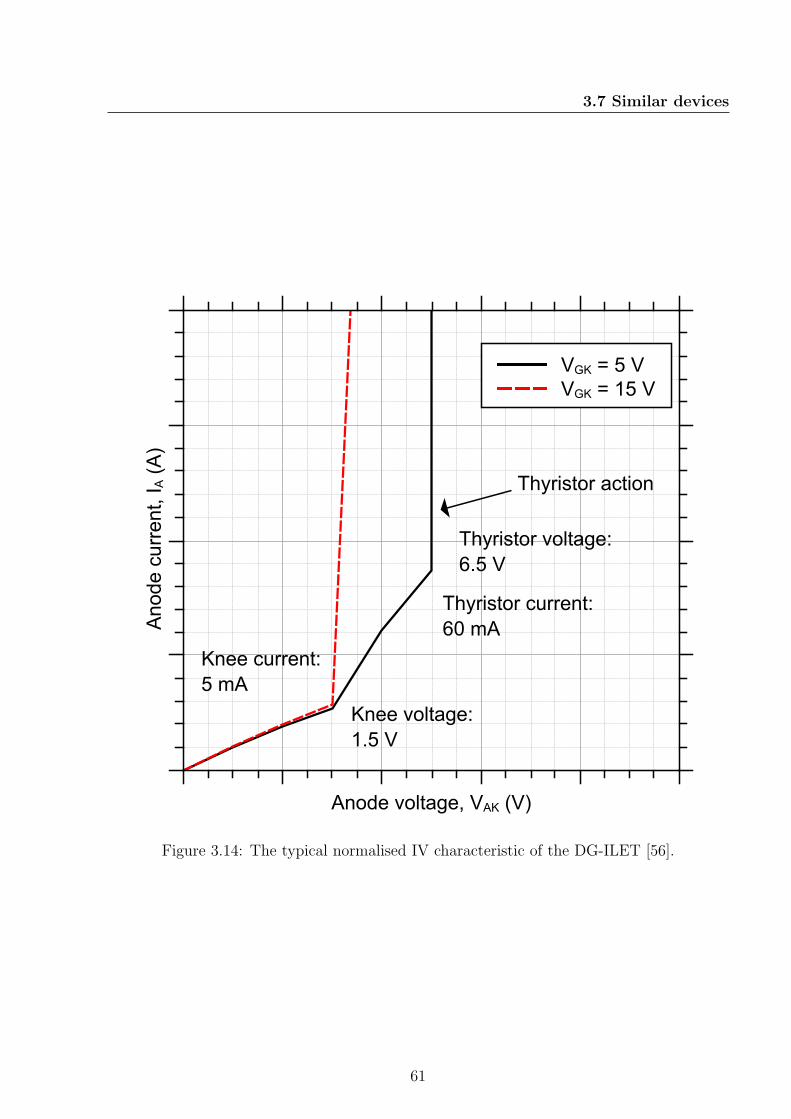
3.7 Similar devices
Anode current, IA (A)
Anode voltage, VAK (V)
VGK = 5 V
VGK = 15 V
Thyristor action
Knee voltage:
1.5 V
Thyristor voltage:
6.5 V
Knee current:
5 mA
Thyristor current:
60 mA
Figure 3.14: The typical normalised IV characteristic of the DG-ILET [56].
61
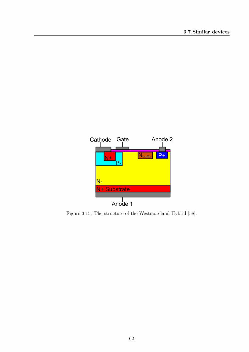
3.7 Similar devices
N+ Substrate
N+P-
N-
Anode 1
GateCathode Anode 2
P+Nbuffer
Figure 3.15: The structure of the Westmoreland Hybrid [58].
62
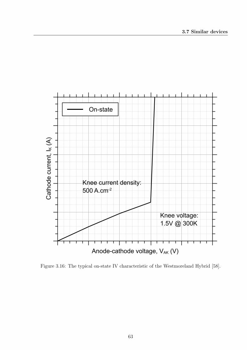
3.7 Similar devices
Cathode current, IK (A)
Anode-cathode voltage, VAK (V)
On-state
Knee voltage:
1.5V @ 300K
Knee current density:
500 A.cm-2
Figure 3.16: The typical on-state IV characteristic of the Westmoreland Hybrid [58].
63

3.8 Potential solutions
3.8 Potential solutions
So what can be done? The DG-ILET and Westmoreland Hybrid show that one solution
to this problem would be to create a hybrid version of two or more switches. A power
MOSFET that also exhibited the high current handling capability of an IGBT at surge
currents would be an ideal solution. The Westmoreland Hybrid offers this solution but with
a lateral structure to give the IGBT characteristic. If the bipolar injection could be moved
to the backside of the device then it could be scaled to much higher currents and voltages.
There has recently been a development in the field of IGBT fabrication that could present
a solution. In order to reduce the thermal mass of the Si substrate, to improve the thermal
performance of the IGBT, several companies have begun using wafer thinning [24,25]. Wafer
thinning is a process by which the substrate wafer is ground and polished until only the bare
minimum of electrical and structural silicon remains. This has given rise to devices fabricated
in wafers that are only as thick as the drift region itself. This has allowed the processing of
the backside of the wafer in ways that had not before been possible. Several companies have
used this new opportunity to fabricate reverse conducting IGBTs (RC-IGBT) [27–30].
The RC-IGBT concept involves using wafer thinning and backside implantation to fabri-
cate an anti-parallel diode within an IGBT. The simplest concept for this is to incorporate a
PiN diode between the collector and emitter in the same way that one appears in the Power
MOSFET. To create this structure the P+ emitter region is replaced with alternating regions
of P+ and N+ where the N+ regions form the PiN diode and the P+ regions form the IGBT,
as seen in Figure 3.17. The Bi-mode Insulated Gate Transistor (BIGT) is an RC-IGBT de-
veloped by ABB. The device is fabricated by thinning the reverse side of the substrate wafer
64

3.8 Potential solutions
Oxide
P+
N+P-
N-
Collector
GateEmitter Emitter
Drift region
P
N+
Figure 3.17: The structure of a reverse conducting IGBT.
to around 100 − 200 µm, depending on the required blocking voltage, and implanting P+
and N+ regions from the reverse side. The device is then optimised to maximise the effective-
ness of the diode without compromising the effectiveness of the IGBT [27–30]. The BIGT is
a device designed for high voltage inductive switching applications. The integrated reverse
conducting diode is present so that discrete diodes are not required in addition to the IGBTs
in power modules. The integration of the diode into the IGBT can save a significant amount
of chip area reducing the size of the power module (provided it can still be sufficiently cooled
from the smaller area). The BIGT and other devices show that it is possible to modify the
backside of an IGBT in order to change it’s properties. These processing techniques are also
commercially viable. If a PiN diode can be integrated in to an IGBT in order to conduct
current in the opposite direction to the IGBT, can an IGBT be integrated into a power
MOSFET so that it will conduct in the same direction as the IGBT? The short answer is
yes. The long answer is contained in chapters 4 - 7. In Chapter 4 this concept, known as
65

3.9 Summary
the Hybrid Unipolar Bipolar Field Effect Transistor (HUBFET) will be introduced and its
structure, mode of operation and fabrication method will be presented.
3.9 Summary
In this chapter, four classes of power semiconductor switch have been presented. Their
various merits have been demonstrated and their suitability as a replacement for the elec-
tromechanical relay in an aircraft EPS has been considered. In each case there is a flaw
some aspect of the device which compromises its suitability for this application. The pro-
posal is that a new device is fabricated that combines the useful properties of two or more
of these devices. This device has been dubbed the HUBFET and will be described in detail
in Chapter 4.
66

Chapter
4 The HUBFET concept
In this chapter the Hybrid Unipolar Bipolar Field Effect Transistor (HUBFET) concept
will be introduced. First, the structure and theory of its operation will be outlined. Finite
element simulations will be used to show how the charge carrier distribution and electrostatic
potential give rise to the HUBFET’s forward on-state IV and transfer characteristics. The
effect of temperature on the on-state IV characteristic will also be investigated through
simulation.
4.1 Basic structure
The HUBFET is a structural merging of the vertical power MOSFET and IGBT. The flow of
current through the device is controlled by the traditional MOS gate structure, as described
in Chapter 3. In the on-state the HUBFET benefits from both unipolar and bipolar conduc-
tion separately depending on the potential at the terminals. Therefore, it is a hybrid, field
effect device, exhibiting both unipolar and bipolar conduction, hence the name HUBFET.
67

4.2 Operation
Oxide
P+
N+P-
N-
Drain
GateSource Source
Drift region
P
N+
Figure 4.1: The structure of the HUBFET
The HUBFET is a combination of the MOSFET and the IGBT each of which have their
own naming convention for their terminals. For the sake of clarity, the HUBFET will take
the naming convention from the power MOSFET, as shown in Figure 4.1. This is because,
operationally the device is a MOSFET that is able to exhibit IGBT characteristics under
particular circumstances as described in its intended application in Chapter 2. Therefore
the HUBFET can be described as a three terminal power switch with source, gate and drain
contacts. The basic structure of the HUBFET is shown in Figure 4.1. It is best to consider
it as a vertical power MOSFET with the alternating P+ and N+ regions between the drain
contact and the drift region.
68

4.2 Operation
4.2 Operation
The structure of the HUBFET is a combination of the structures of a MOSFET and an
IGBT. Similarly the operation can be described in the same way. Figure 4.2 shows the
typical first quadrant IV characteristic of the HUBFET in the on-state, this is very similar
to the Westmoreland hybrid from Chapter 3. It is clearly divided into three distinct regions.
These are the unipolar region, the bipolar region and the saturation region. In this section
the different regions will be explained using the results of finite element analysis performed
in TCAD Sentaurus.
4.2.1 Details of simulation
The HUBFET concept was simulated using the finite element semiconductor simulation
suite TCAD Sentaurus. A 2D representation of the HUBFET structure was built in silicon
using the dimensions and specification found in Figure 4.3 and Table 4.1, and is shown in
Figure 4.4. The drift region thickness (110 µm) and doping concentration (1.43×1014 cm−3)
was chosen using equations 3.2 and 3.3 to give the lowest on-state unipolar resistance for a
blocking voltage of approximately 1290 V . The gate-source structure dimensions were based
on those reported by Bourennane et al [59]. All the results in this chapter were generated
using this model. It was quickly discovered that the drain structure must be very large when
compared to the gate structure for high level injection and conductivity modulation to be
observed. The reasons for this and an analysis of the implications for the design of the device
are shown in Chapter 6. In this chapter, only the fundamental operation of the device will be
discussed. For the purposes of comparison a vertical power MOSFET and IGBT were also
69

4.2 Operation
Table 4.1: The simulation parameters for the HUBFET as shown in Figure 4.3.
Label Description Value
a Half source metal width 7 µm
b Source-gate metal separation 1 µm
c Half gate metal width 10 µm
d Half P+ source width 5 µm
e N+ source width 5 µm
f Channel width 3 µm
g Half channel separation 5 µm
h Half P+ well width 5 µm
i Half cell width 36 µm
j P channel depth 5 µm
k Oxide thickness 0.1 µm
l N+ source depth 1 µm
m P+ well depth 7.5 µm
n Simulation width 360 µm
o Drift region thickness 110 µm
p N+ drain width 180 µm
q P+ drain width 180 µm
A N+ source doping 1.00× 1020 cm−3
B P channel doping 1.00× 1017 cm−3
C P+ well doping 5.00× 1019 cm−3
D N- drift region doping 1.43× 1014 cm−3
E N+ drain doping 1.00× 1020 cm−3
F P+ drain doping 5.00× 1019 cm−3
70

4.2 Operation
independently simulated using the same parameters as in Figure 4.3 and Table 4.1 except for
the MOSFET p = 360 µm and q = 0 µm, and for the IGBT p = 0 µm and q = 360 µm.
4.2.2 Unipolar region
Figure 4.5 shows the HUBFET IV characteristics simulated using the parameters from Ta-
ble 4.1. The first part of the on-state IV curve is the unipolar region. In this region the
HUBFET acts exactly like a MOSFET. Figures 4.6(a), 4.6(b) and 4.6(c) show the electron,
hole and total carrier distribution density in a HUBFET in this region. It is clear that
only one type of carrier (the electron) is contributing to the current flow in the device. In
this region the operation of the device is linear and ohmic. This is because in the current
flowing through the device, and importantly around the P+ drain region, is not sufficient
to lead to enough of a voltage drop to forward bias the PN junction to start the minority
carrier injection. This can be seen in the electrostatic potential plot in Figure 4.8(a). As
the voltage across the device increases the voltage drop around the PN junction at the drain
also increases. Below the bipolar knee voltage this drop is not sufficient to forward bias
the PN junction. In the unipolar region the HUBFET has an advantage over the IGBT as
there is no PN junction in the current path that needs to be overcome before current can
flow. The IV curves of the HUBFET are compared to a power MOSFET, with dimensions
as decribed in Section 4.2.1, in Figure 4.7. The curves show that the pure MOSFET has
a higher current density and therefore lower on-state resistance than the unipolar region of
the HUBFET. This is because the P+ regions at the drain block the conduction path. As a
result, the mean length of current path for the source to the drain is greater in the HUBFET
71

4.2 Operation
than in the MOSFET. This is because some of the charge carriers must travel laterally as
well as vertically in order to reach the drain. This effect will be analysed in Chapter 6.
4.2.3 Bipolar region
As the current through the HUBFET increases, the voltage drop across the P+ region at the
drain also increases. This can be seen in Figures 4.8(a) and 4.8(b). Once this voltage drop
exceeds the threshold voltage of the PN junction, as it has in Figure 4.8(b), the HUBFET
enters bipolar mode or conductivity modulation. Here the IGBT behaviour begins. As the
voltage across the P+ region at the drain is increased the PN junction becomes forwards
biased and the drift region is flooded with both holes and electrons. Figures 4.9(a), 4.9(b)
and 4.9(c) show that, not only are both electrons and holes now contributing to the current
flow, but that the density of carriers is considerably higher than was seen in the unipolar
region in figures 4.6(a), 4.6(b) and 4.6(c). It is this conductivity modulation that gives
the HUBFET its advantage over a standard power MOSFET as it allows significantly more
current to flow without an exponential increase in power loss. The IV curve of the HUBFET
is compared to an equivalent IGBT in Figure 4.7. The bipolar knee voltage of the IGBT
is clearly lower than that of the HUBFET. The PN junction at the drain still requires the
same voltage drop across it to begin bipolar conduction in the HUBFET as in the IGBT.
However, the N+ regions in the HUBFET decrease the portion of the overall total drain-
source voltage drop which biases on the P+ region. Therfore a higher VDS is required to
begin bipolar conduction.
The IGBT portion of the HUBFET behaves like a diode in the on-state. The diode
72

4.2 Operation
current can be extracted from the HUBFET IV curve by removing the unipolar component
of ID using Equation 4.1.
Idiode = ID − VDS
RDS(on)
(4.1)
We can therefore extract some of the bipolar parameters using Equation 4.2.
Idiode = Is. exp
(VAK
η.VT
− 1
)(4.2)
Where Idiode is the diode current, Is is the diode saturation current, η is the diode ideality
factor and VAK is the anode-cathode diode voltage (in this case VAK = VDS). VT is the
thermal voltage given by Equation 4.3 [12].
VT =kT
q(4.3)
Where k is Boltzmanns constant and q is the electron charge. If we take a semi log plot of
the HUBFET IV curve from Figure 4.7 we get the curve shown in Figure 4.10. Equation 4.2
can be rearranged to give Equation 4.4.
log(Idiode) = log(Is) +q
ηkTVAK (4.4)
From Equation 4.4 and Figure 4.10 we can extract a value for η. Typically if η ≈ 1
then Idiode is from diffusion current. As η increases and tends towards 2 then the majority of
Idiode is from high level injection. High level injection is seen in bipolar devices and indicated
73

4.2 Operation
that the drift region of the device is conductivity modulated. In the case of the HUBFET
simulation here, η ≈ 2.01 for 1.0 V < VDS < 1.5 V . This shows the HUBFET is utilising
majority carrier conduction at higher voltages.
4.2.4 Saturation region
As the voltage across the device increases further, saturation of the channel is reached. Now
the drift region is almost completely flooded with carriers as shown in figures 4.11(a), 4.11(b)
and 4.11(c). The current flow is limited by the channel and the number of carriers in the
drift region can no longer increase. The saturation of the channel in the HUBFET follows
the IGBT channel saturation model shown in Equation 4.5 based on the BJT/MOSFET
model shown in Figure 4.12 [23].
ID =1
1− αPNP
µCHCoxZ
2LCH
(VGS − Vth)2 (4.5)
Where ID is the drain current in the HUBFET, µCH is the carrier mobility in the channel,
Cox is the oxide capacitance, Z is the orthogonal depth of the channel, LCH is the channel
length αPNP is the gain of the PNP transistor from Figure 4.12. The saturation current
of the HUBFET is therefore higher than the equivalent saturation current of a standard
MOSFET. This means the HUBFET will be capable of considerably higher current densities
than a traditional power MOSFET, or a superjunction MOSFET, for the same channel area.
74
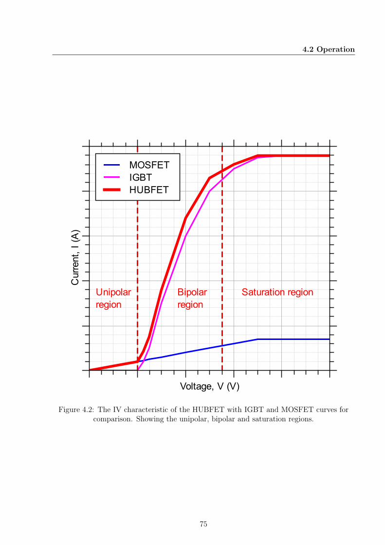
4.2 Operation
Current, I (A)
Voltage, V (V)
MOSFET
IGBT
HUBFET
Saturation regionBipolar
region
Unipolar
region
Figure 4.2: The IV characteristic of the HUBFET with IGBT and MOSFET curves forcomparison. Showing the unipolar, bipolar and saturation regions.
75
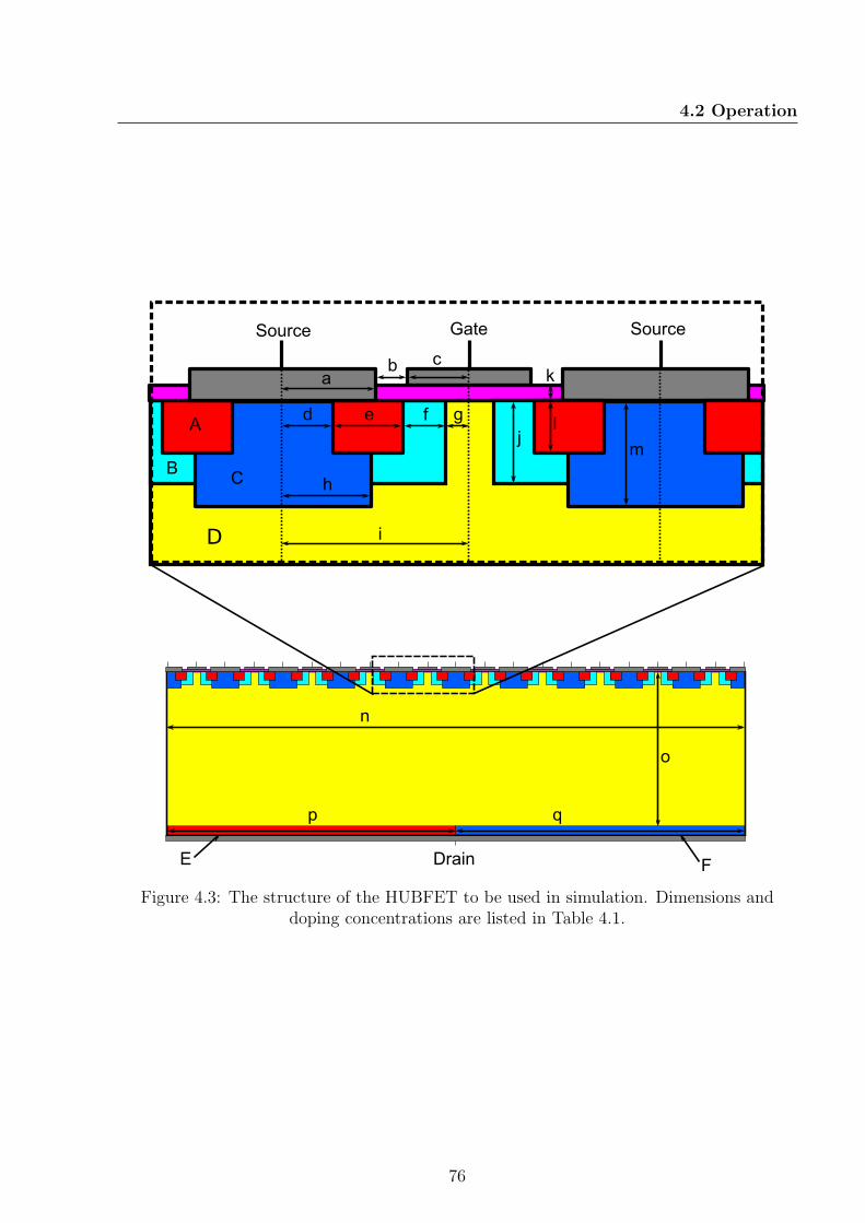
4.2 Operation
GateSource Source
D
CB
A
ab c
d e f g
h
i
j
k
l
m
n
o
p q
DrainE F
Figure 4.3: The structure of the HUBFET to be used in simulation. Dimensions anddoping concentrations are listed in Table 4.1.
76
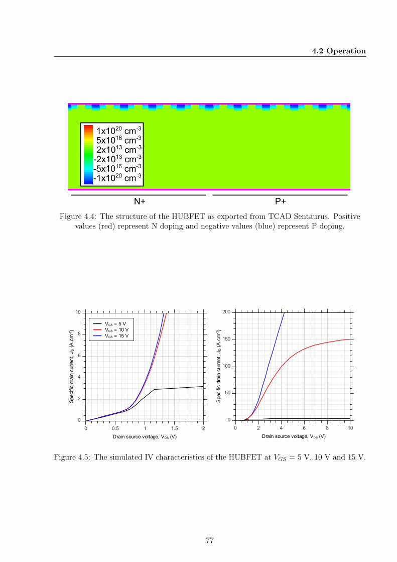
4.2 Operation
1x10²⁰
cm-3
-1x10²⁰
cm-3
-5x10¹⁶
cm-3
5x10¹⁶
cm-3
2x10¹³
cm-3
-2x10¹³
cm-3
N+ P+
Figure 4.4: The structure of the HUBFET as exported from TCAD Sentaurus. Positivevalues (red) represent N doping and negative values (blue) represent P doping.
Sp
ec
ific
dra
in c
urr
en
t, J
D (
A.c
m-2
)
0
2
4
6
8
10
Drain source voltage, VDS (V)
0 0.5 1 1.5 2
VGS = 5 V
VGS = 10 V
VGS = 15 V
Specific drain current, J
D (A.cm
-2)
0
50
100
150
200
Drain source voltage, VDS (V)
0 2 4 6 8 10
Figure 4.5: The simulated IV characteristics of the HUBFET at VGS = 5 V, 10 V and 15 V.
77
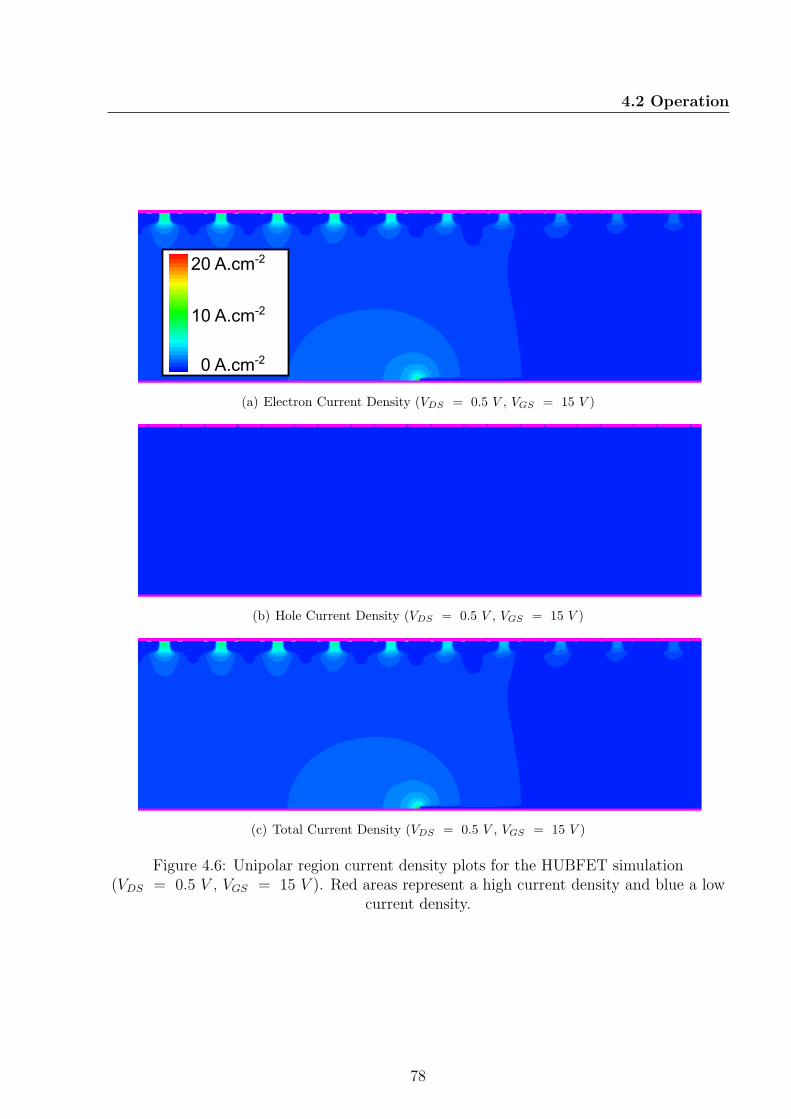
4.2 Operation
20 A.cm-2
0 A.cm-2
10 A.cm-2
(a) Electron Current Density (VDS = 0.5 V , VGS = 15 V )
(b) Hole Current Density (VDS = 0.5 V , VGS = 15 V )
(c) Total Current Density (VDS = 0.5 V , VGS = 15 V )
Figure 4.6: Unipolar region current density plots for the HUBFET simulation(VDS = 0.5 V , VGS = 15 V ). Red areas represent a high current density and blue a low
current density.
78
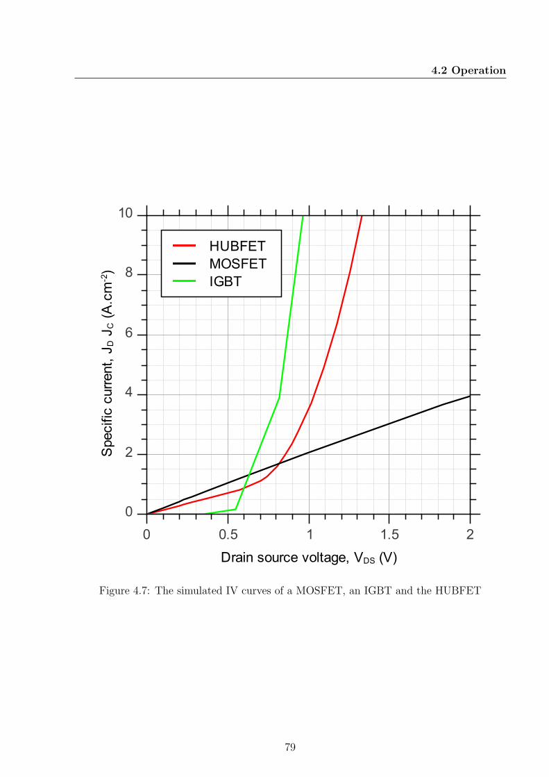
4.2 Operation
Sp
ec
ific
cu
rre
nt,
JD
JC
(A
.cm
-2)
0
2
4
6
8
10
Drain source voltage, VDS (V)
0 0.5 1 1.5 2
HUBFET
MOSFET
IGBT
Figure 4.7: The simulated IV curves of a MOSFET, an IGBT and the HUBFET
79
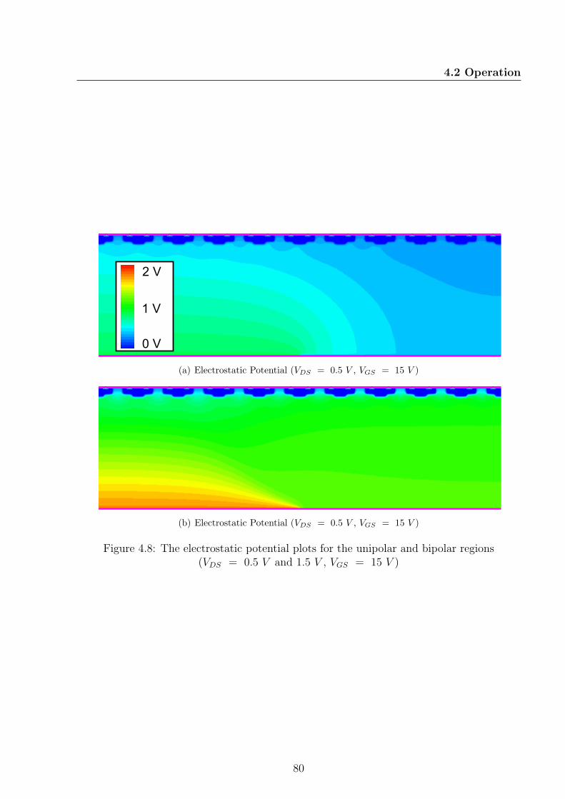
4.2 Operation
2 V
0 V
1 V
(a) Electrostatic Potential (VDS = 0.5 V , VGS = 15 V )
(b) Electrostatic Potential (VDS = 0.5 V , VGS = 15 V )
Figure 4.8: The electrostatic potential plots for the unipolar and bipolar regions(VDS = 0.5 V and 1.5 V , VGS = 15 V )
80
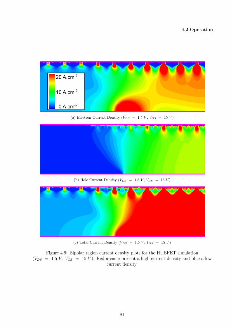
4.2 Operation
20 A.cm-2
0 A.cm-2
10 A.cm-2
(a) Electron Current Density (VDS = 1.5 V , VGS = 15 V )
(b) Hole Current Density (VDS = 1.5 V , VGS = 15 V )
(c) Total Current Density (VDS = 1.5 V , VGS = 15 V )
Figure 4.9: Bipolar region current density plots for the HUBFET simulation(VDS = 1.5 V , VGS = 15 V ). Red areas represent a high current density and blue a low
current density.
81
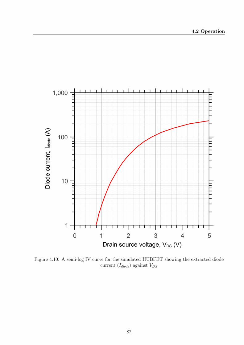
4.2 Operation
Diode current, Idiode (A)
1
10
100
1,000
Drain source voltage, VDS (V)
0 1 2 3 4 5
Figure 4.10: A semi-log IV curve for the simulated HUBFET showing the extracted diodecurrent (Idiode) against VDS
82
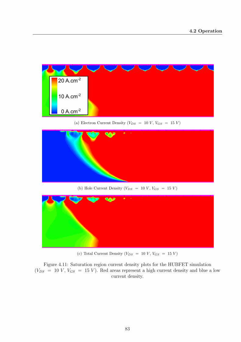
4.2 Operation
20 A.cm-2
0 A.cm-2
10 A.cm-2
(a) Electron Current Density (VDS = 10 V , VGS = 15 V )
(b) Hole Current Density (VDS = 10 V , VGS = 15 V )
(c) Total Current Density (VDS = 10 V , VGS = 15 V )
Figure 4.11: Saturation region current density plots for the HUBFET simulation(VDS = 10 V , VGS = 15 V ). Red areas represent a high current density and blue a low
current density.
83
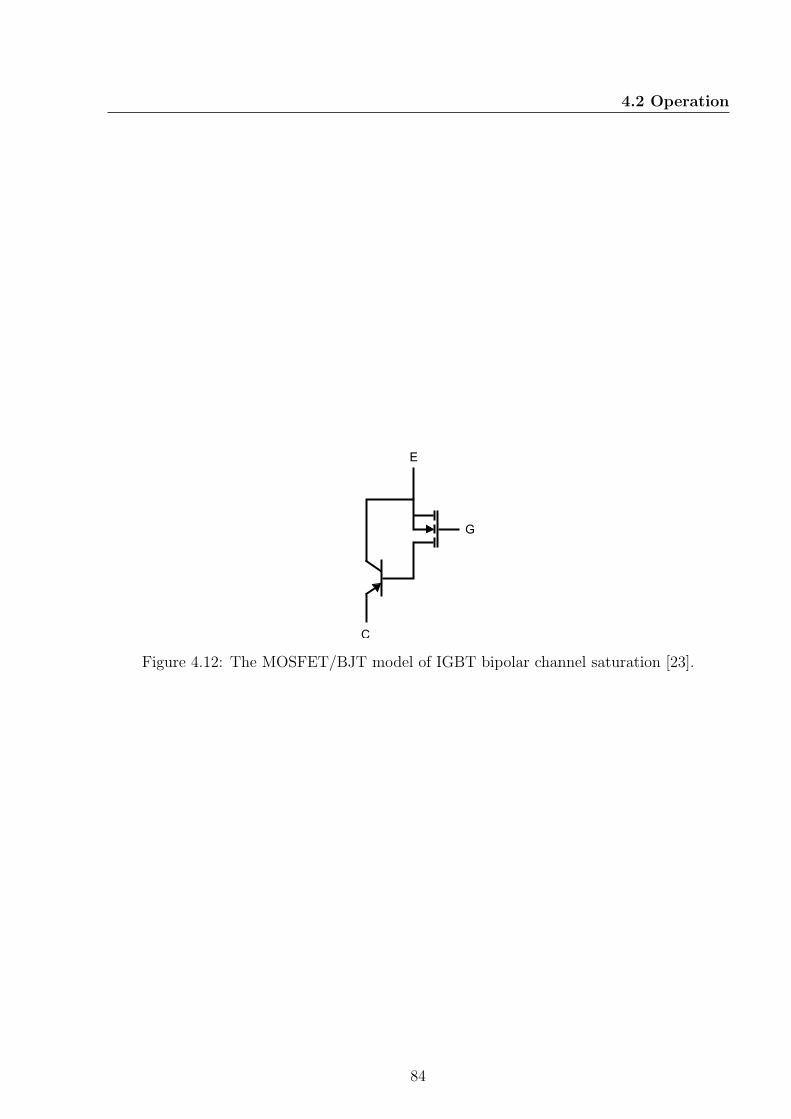
4.2 Operation
G
E
C
Figure 4.12: The MOSFET/BJT model of IGBT bipolar channel saturation [23].
84
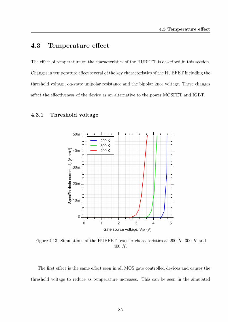
4.3 Temperature effect
4.3 Temperature effect
The effect of temperature on the characteristics of the HUBFET is described in this section.
Changes in temperature affect several of the key characteristics of the HUBFET including the
threshold voltage, on-state unipolar resistance and the bipolar knee voltage. These changes
affect the effectiveness of the device as an alternative to the power MOSFET and IGBT.
4.3.1 Threshold voltage
Specific drain current, J
D (A.cm
-2)
0
10m
20m
30m
40m
50m
Gate source voltage, VGS (V)
0 1 2 3 4 5
200 K
300 K
400 K
Figure 4.13: Simulations of the HUBFET transfer characteristics at 200 K, 300 K and400 K.
The first effect is the same effect seen in all MOS gate controlled devices and causes the
threshold voltage to reduce as temperature increases. This can be seen in the simulated
85

4.3 Temperature effect
transfer characteristic curves in Figure 4.13. The equation for threshold voltage is given in
Equation 4.6 [4].
Vth =toxεox
√4εskTNA ln
(NA
ni
)(4.6)
Where tox is the oxide thickness, εs is the relative permittivity of the semiconductor, εox
is the relative permittivity of the oxide, k is Boltzmanns constant, T is the temperature,
NA is the doping concentration of the channel and ni is the intrinsic carrier concentration
of the semiconductor. The temperature dependence of the threshold voltage comes mostly
from the temperature dependence of the intrinsic carrier concentration which is given in
Equation 4.7 [60].
ni = (NC .NV )1/2 exp
(− Eg
2kT
)(4.7)
Where NC is the density of states in the conduction band, NV is the density of states in
the valence band and Eg is the energy bandgap. NC , NV and Eg are all also temperature
dependent. This temperature dependence is given in equations 4.8, 4.9 and 4.10 [60].
NC = 6.2× 1015.T 3/2 (4.8)
NV = 3.5× 1015.T 3/2 (4.9)
Eg = 1.17− 4.73× 10−4.T 2/(T+636) (4.10)
86

4.3 Temperature effect
The combination of these effects leads to the reduction in Vth with increasing temperature
as seen in Figure 4.13. This change is significant as over the maximum operating range of
the switch (−75 oC to +125 oC) Vth varies by over 1 V . If the device is only ever hard on
or hard off, this will not present a problem. However, if the device is linearly controlled to
limit current flow, care must be taken over control system design and device choice. This is
especially true if several devices are to be used in parallel [61,62]. This change in threshold
voltage with temperature is the same for all MOS gated devices and so will not disadvantage
the HUBFET when compared to the power MOSFET or IGBT.
4.3.2 Unipolar on-state resistance
Sp
ec
ific
dra
in c
urr
en
t, J
D (
A.c
m-2
)
0
2
4
6
8
10
Drain source voltage, VDS (V)
0 0.5 1 1.5 2
200 K
300 K
400 K
Figure 4.14: Simulations of the HUBFET IV characteristics at 200 K, 300 K and 400 K(VGS = 15 V ).
87

4.3 Temperature effect
The unipolar on-state resistance is also affected by temperature. This change is due to
the increase in resistivity of the drift region and other areas of the current path, due to the
rising temperature. This increase in resistivity is in turn due to the reduction in carrier
mobility due to the increasing temperature and is given by Equation 4.11 [63–66].
ρ =1
q(µnn+ µpp)(4.11)
Where ρ is the resistivity of the semiconductor, µn is the mobility of the electrons,
n is number of electrons, µp is the mobility of the holes and p is the number of holes.
The effect caused by this temperature dependence can be seen in the unipolar region of
Figure 4.14. As the temperature increases, the on-state resistance the unipolar region also
increases which increases the power loss in the device for a given current. This behaviour
will reduce the MOSFET region advantage of the HUBFET over a straight IGBT solution.
Power MOSFETs operating in parallel in the ohmic region of the IV characteristic are able
to self balance current between themselves. This is due to the increase in resistivity with
temperature. If a MOSFET conducts more current it will heat up, increasing its resistance
and limiting the current flow relative to the other devices, quickly finding an equilibrium.
This self balancing in the ohmic region is retained by the HUBFET in the unipolar region.
4.3.3 Bipolar knee voltage
Although the resistance of the unipolar region increases with increasing temperature, the
bipolar knee voltage reduces as seen in Figure 4.14. This can be attributed to the temperature
dependence of the diode saturation current (Is) in Equation 4.2 [12], also known as the
88

4.3 Temperature effect
Shockley equation, and can be seen in Figure 4.14. In this case the diode being referred to
is the PN junction between the P+ regions at the HUBFET drain and the N- drift region.
This reduction in bipolar knee voltage appears to negate the benefit of the self balancing
effect detailed in Section 4.3.2 observed in the unipolar resistance. As current in a device
causes it to heat up, the bipolar knee voltage reduces. If several HUBFETs are operating in
parallel, this could lead to the bipolar action starting in one device before the others meaning
it conducts the bulk of the current. However, as this increase is due to bipolar conduction
it will not result in the same exponential increase in power loss as seen in MOSFETs.
4.3.4 Bipolar differential resistance
Sp
ec
ific
dra
in c
urr
en
t, J
D (
A.c
m-2
)
0
20
40
60
80
100
Drain source voltage, VDS (V)
0 1 2 3 4
200 K
300 K
400 K
Figure 4.15: Simulations of the HUBFET IV characteristics at 200 K, 300 K and 400 K(VGS = 15 V ) showing the high current bipolar region.
89

4.4 Fabrication
The bipolar differential resistance is also affected by temperature through the same mech-
anism as the unipolar on-state resistance. However, as the bipolar differential resistance is
generated by both types of carriers it does not follow such a straight forward increase as the
unipolar resistance. The higher differential resistance seen at 200 K seems unexpected when
compared to the relationship between unipolar resistance and temperature. The increase in
bipolar differential resistance is likely due to the fact that the increase in mobility caused by
the decrease in temperature is outweighed by the decrease in carriers because of the increase
in bipolar knee voltage described in Section 4.3.3. These effects combine into the increase
in resistivity seen in Figure 4.15. Over the wide temperature range simulated (−75 oC to
+125 oC) the change in bipolar differential resistance is not sufficient to cause concern.
4.4 Fabrication
The proposed HUBFET has a similar structure to that of Reverse conducting IGBTs such as
the ABB BIGT introduced in Section 3.8 and shown in Figure 3.17. The BIGT has a ratio of
around 80% P+ doping to 20% N+ doping at the collector where the P+ area provides the
IGBT characteristic and the N+ provides the reverse conducting diode characteristic. The
reported IV curves appear to show a small amount of MOSFET action in the forward current
path. However they can also exhibit a strong snapback effect [29]. Due to the similarity
between the simulated HUBFET structure and the BIGT structure, it was proposed that
the BIGT fabrication technique should be used to produce some proof of concept HUBFET
switches.
90

4.5 Summary
4.5 Summary
In this chapter the theoretical and simulated operation of the HUBFET has been introduced.
The effects of temperature on the on-state characteristics of the HUBFET have been simu-
lated. The effects of temperature on the threshold voltage and bipolar differential resistance
are not significant when considering the HUBFET as a replacement for a power MOSFET
or an IGBT. The change in bipolar knee voltage and unipolar resistance could lead to con-
trol issues when running several devices in parallel. The similarity between the BIGT and
HUBFET structure has led to the BIGT fabrication process being used to fabricate some
proof of concept HUBFET switches. These switches will be discussed in Chapter 5. Modifi-
cations to the structure of these proof of concept devices and how those modifications may
improve the devices operation will be discussed in Chapter 6. The simulation results shown
in this chapter were presented by the author as part of a paper at APEC 2012 [67].
91

Chapter
5Testing of the proof of concept
HUBFET devices
In this chapter the HUBFET concept is put to the test. Two prototype HUBFET modules
were manufactured for this work. The test modules, each consisting of 5 die, where each die
has an active area of 1.44 cm2, were manufactured by ABB specifically for this project. The
devices were tested to measure their forward on-state IV characteristic. For comparison a
1200 V off-the-shelf MOSFET and IGBT were also tested. This work was used to validate the
simulations and the theory from Chapter 4. The results of the on-state measurements of the
HUBFET were published by the author in the Proceedings of the Applied Power Electronics
Conference and Exposition in February 2012 in Orlando, Florida [67]. Additionally, a high
energy short circuit test was devised to ensure the HUBFET is able to dynamically transition
from unipolar to bipolar mode and be reliably turned off during a short circuit event.
92

5.1 The HUBFET prototype
5.1 The HUBFET prototype
The prototype test modules used in this section were manufactured by ABB using their BIGT
fabrication process as described in briefly in Section 3.8. The BIGT uses alternating areas
of P+ and N+ doping at the collector terminal of an IGBT to integrate a reverse conducting
PiN diode in to the structure of the switch. This is achieved through a combination of a
conventional MOS gate process applied to the topside of the wafer and a two mask backside
implantation process, where one mask is used to implant the P+ regions and the inverse
of the mask is used for the N+ regions. The P+ area at the collector of the BIGT is
proportionally larger than the area of N+. For the HUBFET prototype devices the P+ and
N+ masks from the BIGT process were reversed giving approximately 80% N+ area to 20%
P+ area. The pattern used for these implants was the radial layout as used in [30] and
shown in Figure 5.1. Optimising this pattern for use in the HUBFET is studied in detail
in Chapter 6. This solution of piggybacking an existing process represents the fastest and
most cost effective path to proving the feasibility of the concept design. A photograph of
one of the experimental HUBFET modules is shown in Figure 5.2. The module consists of
six die each with an active area of 1.44 cm2. The drain contact of the die are soldered to a
copper plate attached to a ceramic substrate. The source and gate contacts are wire bonded
to more islands of copper which can be seen in the photograph. During the bonding process
one of the die was electrically damaged. This device was electrically isolated leaving the
module with five working die with a combined active area of 7.2 cm2.
93
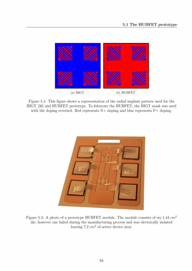
5.1 The HUBFET prototype
(a) BIGT (b) HUBFET
Figure 5.1: This figure shows a representation of the radial implant pattern used for theBIGT [30] and HUBFET prototype. To fabricate the HUBFET, the BIGT mask was used
with the doping reversed. Red represents N+ doping and blue represents P+ doping.
Figure 5.2: A photo of a prototype HUBFET module. The module consists of six 1.44 cm2
die, however one failed during the manufacturing process and was electrically isolatedleaving 7.2 cm2 of active device area.
94

5.2 Forward on-state characteristic
Table 5.1: This table shows the different parameters for the devices used for comparison inthis chapter
Device PackageActive Area
(cm2)
Maximumrated current
(A)
MeasuredBreakdownVoltage (V )
HUBFET Direct copper bondtest package
7.2 - 1398
MOSFET PLUS-247 1.26 20 1280
IGBT TO-247 0.36 60 1288
5.2 Forward on-state characteristic
In order to analyse the suitability of the HUBFET as a failure tolerant power switch for use in
the application described in Chapter 2, it was necessary to analyse its on-state performance.
5.2.1 Method
The on-state characteristics of the HUBFET prototype were measured using a Tektron-
ics 371b Power Curve tracer at room temperature. For comparison, a power MOSFET
and IGBT were also measured. They were an IXYS IXFX20N120 1200 V vertical Power
MOSFET [68] and an International Rectifier IRGP30B120KD-EP 1200 V IGBT [69]. Ta-
ble 5.1 shows a comparison of the parameters of the different devices. The curve tracer
measures the on-state characteristic of the switch by fixing the gate voltage (VGS or VGE)
at the desired level (in all the following cases it is 15 V ), the potential across the power
terminals (VDS or VCE) is then pulsed with the voltage increasing with each pulse. The
current is measured during each pulse and the voltage and current are plotted against each
other to give the on-state IV characteristic of the device.
95

5.2 Forward on-state characteristic
5.2.2 Results
Figure 5.3 shows the room temperature forward IV characteristic of the HUBFET, the
IXYS MOSFET and the IR IGBT. The current measurements for each device have been
scaled by device area to compare the devices by their specific current density, JD for the
MOSFET and HUBFET and JC for the IGBT, in A.cm−2. The measured RDS(on)sp of the
MOSFET is 0.85 Ω.cm2 compared to 1.05 Ω.cm2 in the unipolar region for the HUBFET.
Although these values are similar, the MOSFET has a marginally lower RDS(on). This is
most likely due to the P+ regions at the drain terminal of the HUBFET increasing the
HUBFET RDS(on)sp. Additionally the HUBFET has a higher measured breakdown voltage
(VBR) than the MOSFET and IGBT. This means the HUBFET has either a thicker or
more lightly doped drift region than the IGBT and MOSFET. This will also contribute to
its higher RDS(on)sp. When the bipolar characteristics are compared, Vk for the IGBT is
0.5 V and for the HUBFET is 1.0 V . However the HUBFET prototype clearly works as
expected. It has a clear unipolar ohmic region which, as VDS is increased, gives way to
a sharp rise in ID which is characteristic of minority carrier injection. Figure 5.3 can be
compared with the simulations from Chapter 4 in figures 4.2 and 4.7. The simulations from
Chapter 4 over estimate the performance of each of the devices, reporting consistently lower
values for RDS(on) and Vk. This is likely due to the idealised nature of the simulations. The
simulations do not include any edge termination, which is required in real devices to maintain
the blocking voltage. They also do not include any circuit or packaging resistances that are
present in true devices. As a result both RDS(on) and Vk are higher in the measured devices
than they are in the simulation. However, there is still an extremely strong correlation
96

5.2 Forward on-state characteristic
between the theory, simulated results and experimental data.
97
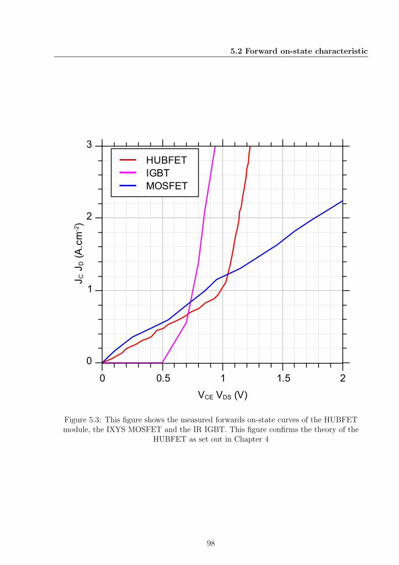
5.2 Forward on-state characteristic
JC JD (A.cm-2)
0
1
2
3
VCE VDS (V)
0 0.5 1 1.5 2
HUBFET
IGBT
MOSFET
Figure 5.3: This figure shows the measured forwards on-state curves of the HUBFETmodule, the IXYS MOSFET and the IR IGBT. This figure confirms the theory of the
HUBFET as set out in Chapter 4
98

5.3 High energy short circuit test
5.3 High energy short circuit test
Having verified that the HUBFET performs as the simulations from Chapter 4 suggested,
it was decided determine if the device was able to perform the function for which it was
initially envisaged. As described in Chapter 2, the HUBFET is designed to operate in a
smart circuit breaker system. It must operate at low currents with low on-state losses whilst
being able to survive high energy short circuit events. It must also dynamically transition
between the two operating modes without additional input from the gate and be reliably
turned off during a high energy transient.
5.3.1 Method
To test the short circuit capability of the HUBFET, an experiment was devised. A bespoke
test rig was built and connected to an ET System LabHP 10100 100 V /100 A 10 kW power
supply. The data was recorded using a Tektronix TDS5054B Digital Phosphor Oscilloscope.
The test rig design is shown in Figure 5.4.
The experimental set up uses two resistors and an OMRON G9EC-1-B electromechanical
relay to dynamically switch between nominal an short circuit conditions. The control signals
used for this test are shown in Figure 5.5 and Table 5.2 lists the circuit variables and their
values.
Initially, at t = t0 the device under test (DUT) is off, the device is turned on in series
with the 100 Ω resistor allowing a small current to flow at t = t1. After a set time, at t = t2
the electromechanical relay switches the 1 Ω resistor in parallel with the 100 Ω resistor. This
dramatically increases the current flowing through the DUT. The DUT is turned off at t = t3
99
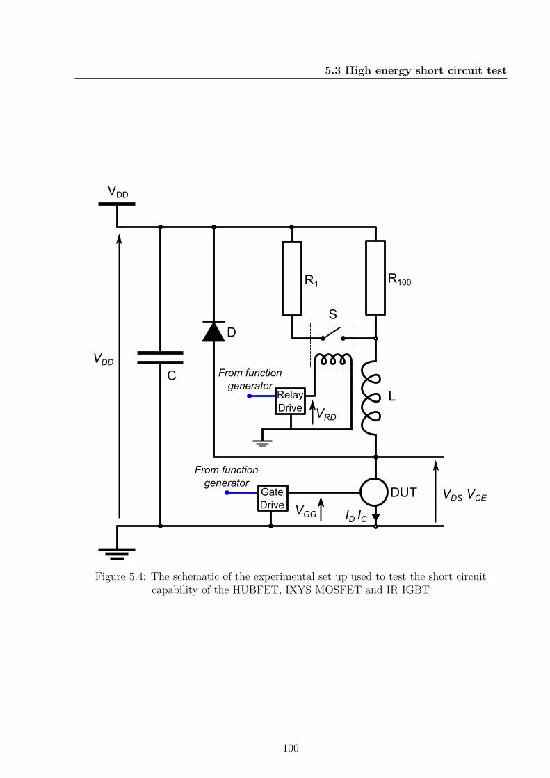
5.3 High energy short circuit test
C
L
DUT
D
S
R1 R100
VDD
ID IC
VDS VCE
VDD
Gate
Drive VGG
From function
generator
Relay
DriveVRD
From function
generator
Figure 5.4: The schematic of the experimental set up used to test the short circuitcapability of the HUBFET, IXYS MOSFET and IR IGBT
100
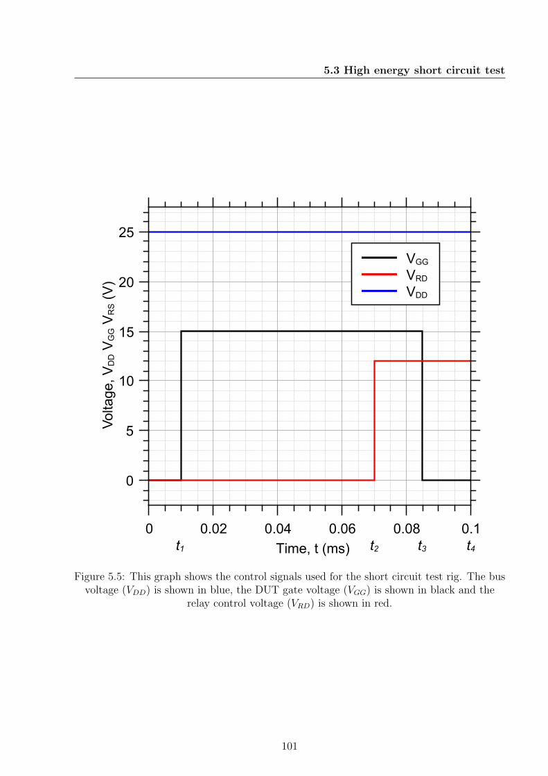
5.3 High energy short circuit test
Voltage, VDD V
GG V
RS (V)
0
5
10
15
20
25
Time, t (ms)
0 0.02 0.04 0.06 0.08 0.1
VGGVRDVDD
t1 t2 t3 t4
Figure 5.5: This graph shows the control signals used for the short circuit test rig. The busvoltage (VDD) is shown in blue, the DUT gate voltage (VGG) is shown in black and the
relay control voltage (VRD) is shown in red.
101

5.3 High energy short circuit test
Table 5.2: This table lists the circuit parameters and variables used during the short circuittesting of the 3 power devices. The values refer to the diagram in Figure 5.4 and the graph
in Figure 5.5
.
Parameter Description Value
VDD Bus voltage from power supply 25 V
VFG Function generator output voltage 5 V
VGG DUT gate drive voltage 15 V
VRD Relay Drive voltage 12 V
C Slew compensation capacitance 5 mF (5× 1 mF )
L Inductance 100 µH
R1 Short circuit resistor 1 Ω
R100 Nominal load resistor 100 Ω
t0 Start of measurements 0 ms
t1 Turn on DUT 10 ms
t2 Turn on relay (start of short circuit) 70 ms
t3 Turn off DUT 85 ms
t4 Turn off relay 90 ms
and the current reduces to zero. The capacitor bank across the power terminals compensates
for the slew rate of the power supply allowing the current to respond rapidly to the sudden
change in circuit resistance that occurs when the relay is switched. The inductor is present
to allow other circuit inductances to be ignored as they become negligible when compared
to L. The diode commutates the current from the inductor when the DUT is turned off
in order to prevent large voltage spikes from destroying the DUT. A Tektronix AFG3022
Dual Channel Arbitrary/Function generator was used to provide the control signals to the
DUT and the relay. The main power supply was controlled over GPIB by a laptop running a
custom Labview VI. The current was measured on the power cable running from the DUT to
ground with a Tektronix TCP303 hall effect current probe and TCPA300 current amplifier.
102

5.3 High energy short circuit test
The voltage across the DUT (VDS or VCE) and the bus voltage (VDD) were measured using
Tektronix 020-2195-00 2200 V CAT II differential probes and P5210 Filter/Amplifiers. The
DUT gate control signal was connected directly from the function generator to the scope
to provide a timing reference for the test. Three of each of the MOSFET and IGBT were
measured as was one HUBFET module. The results from the tests are discussed in the next
section.
5.3.2 Results
For each short circuit measurement, a zero voltage calibration was taken. All power supplies
in the circuit were enabled but set to 0 V . The voltage measured was measured on each of
the differential probes and this voltage was taken as 0 V . For the current probe, the zero
calibration was performed during the measurement trace. The value on the current probe
for t0 < t < t1 was filtered for noise and taken as 0 A. Due to the large difference
between the nominal and short circuit currents measured during this test, it was necessary
to perform the test on each device twice using a different resolution on the current probe for
each measurement.
MOSFET
Figure 5.6 shows the average of the measurements from the three IXYS MOSFETs with the
high frequency noise removed. The performance of the three devices was identical for all
intents and purposes. The high current short circuit is clear, however the low current flowing
for t1 < t < t2 is lost in the noise of the current probe.
103
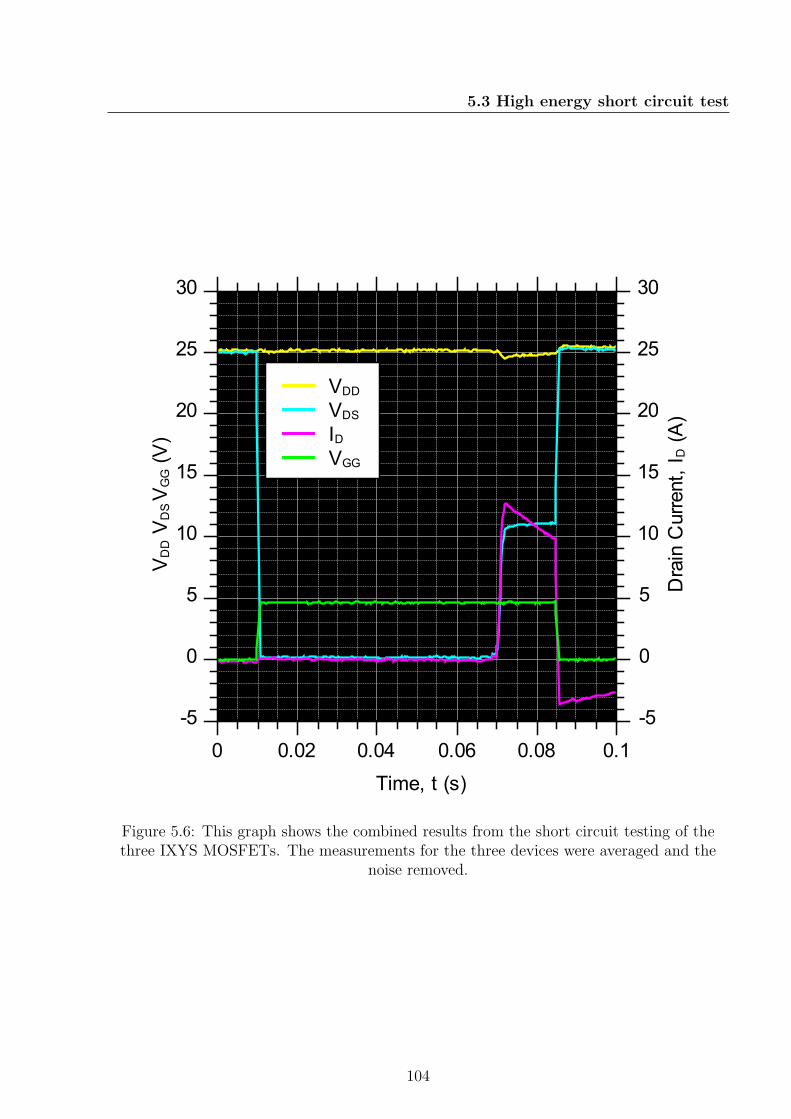
5.3 High energy short circuit test
VDD V
DS VGG (V)
-5
0
5
10
15
20
25
30
Drain Current, ID (A)
-5
0
5
10
15
20
25
30
Time, t (s)
0 0.02 0.04 0.06 0.08 0.1
VDDVDSIDVGG
Figure 5.6: This graph shows the combined results from the short circuit testing of thethree IXYS MOSFETs. The measurements for the three devices were averaged and the
noise removed.
104

5.3 High energy short circuit test
Figure 5.7 shows results from a repeat of the same test as Figure 5.6 but with ID and
VDS rescaled to show the low current performance of the device.
It is clear from these graphs that although the device is performing well, with low losses
during the low current test, the power loss is extremely high during the high current part of
the test. This is due to the very high VDS as a result of the ohmic behaviour of the device.
The change in VDS and ID observed during the short circuit is likely due to the resistance of
the MOSFET increasing with temperature due to the high power dissipation combined with
the inductor de-energising. The relationship between VDS and ID for the MOSFET seen in
this test is consistent with the on-state measurements shown in Figure 5.3.
IGBT
Figures 5.8 and 5.9 show the results of the short circuit tests for the three IR IGBTs. As
with the MOSFETs, the measurements from the three IGBTs were effectively identical. The
traces were averaged and filtered for high frequency noise.
Here the IGBTs exhibit a higher voltage drop than the MOSFETs for the same current
during the low current period of the test and a lower drop for a higher current during the high
current period of the test. Both of these differences can be attributed to the bipolar action of
the device. The higher voltage drop at low currents is due to the PN junction at the collector
of the device. The voltage drop at high currents is due to the bipolar conduction that is
made possible by the same PN junction. As with the MOSFETs this result is consistent
with the measured IV characteristic for the IGBT as shown in Figure 5.3.
105
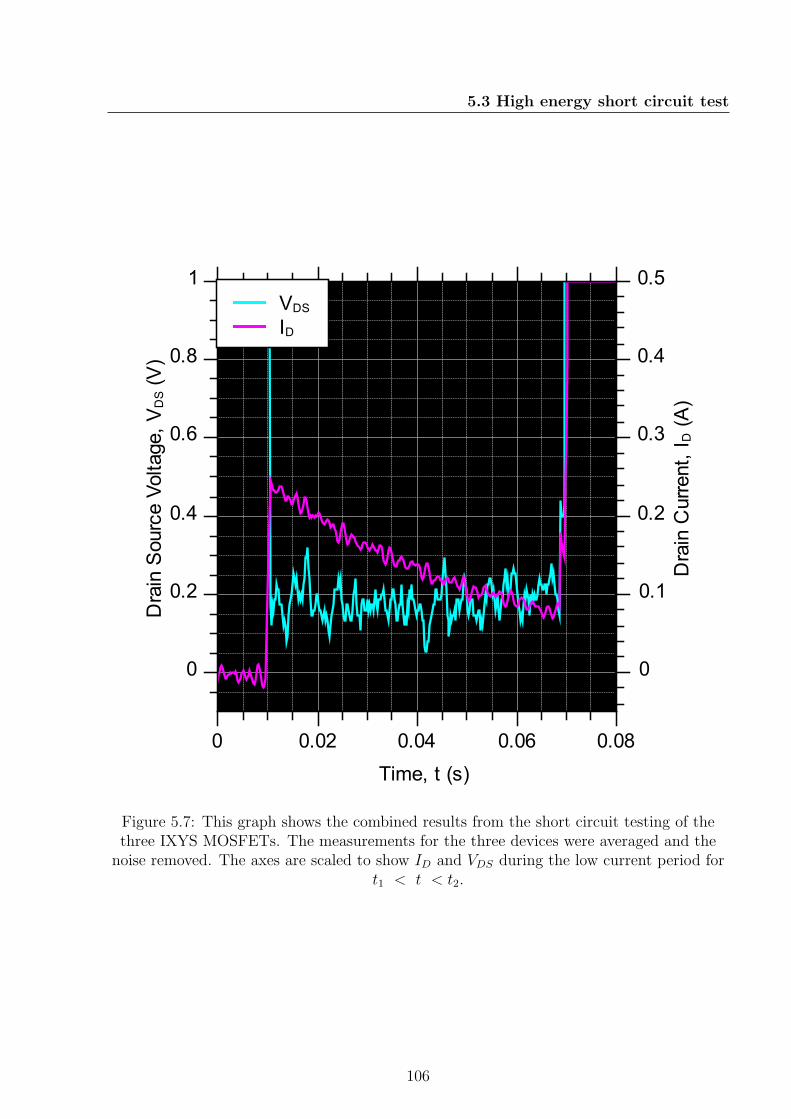
5.3 High energy short circuit test
Drain Source Voltage, VDS (V)
0
0.2
0.4
0.6
0.8
1
Drain Current, ID (A)
0
0.1
0.2
0.3
0.4
0.5
Time, t (s)
0 0.02 0.04 0.06 0.08
VDSID
Figure 5.7: This graph shows the combined results from the short circuit testing of thethree IXYS MOSFETs. The measurements for the three devices were averaged and the
noise removed. The axes are scaled to show ID and VDS during the low current period fort1 < t < t2.
106
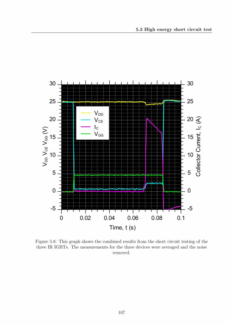
5.3 High energy short circuit test
VDD V
CE V
GG (V)
-5
0
5
10
15
20
25
30
Collector Current, IC (A)
-5
0
5
10
15
20
25
30
Time, t (s)
0 0.02 0.04 0.06 0.08 0.1
VDD
VCE
ICVGG
Figure 5.8: This graph shows the combined results from the short circuit testing of thethree IR IGBTs. The measurements for the three devices were averaged and the noise
removed.
107
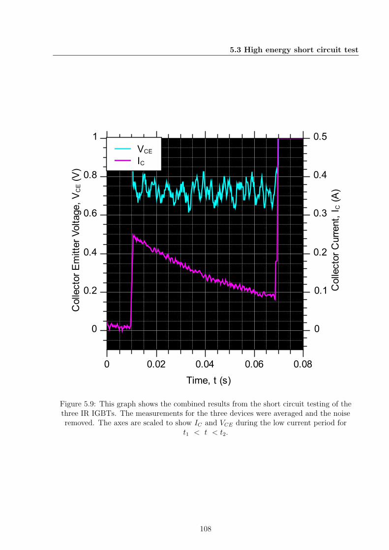
5.3 High energy short circuit test
Collector Emitter Voltage, V
CE (V)
0
0.2
0.4
0.6
0.8
1
Collector Current, I
C (A)
0
0.1
0.2
0.3
0.4
0.5
Time, t (s)
0 0.02 0.04 0.06 0.08
VCE
IC
Figure 5.9: This graph shows the combined results from the short circuit testing of thethree IR IGBTs. The measurements for the three devices were averaged and the noiseremoved. The axes are scaled to show IC and VCE during the low current period for
t1 < t < t2.
108

5.3 High energy short circuit test
HUBFET
Figures 5.10 and 5.11 show the short circuit performance of one of the HUBFET modules.
Here the high current plot in Figure 5.10 shows a relatively small voltage drop across the
device compared to the MOSFET. In Figure 5.11, during the low current phase the voltage
drop is small compared to the IGBT. The voltage drop across the HUBFET of approximately
0.2 V in the low current portion of the test is lower than Vk which was measured in Section
5.2.2 as 1.0 V . This means that the device is operating in unipolar mode during this phase
of the test. During the high current phase the voltage drop does not increase linearly with
the increase in current. VDS increases to 3 V while ID increases to 20 A. Therefore the
device is operating in bipolar mode. This is consistent with the theory from Chapter 4 and
from the IV measurements from Section 5.2.2 of this chapter.
109
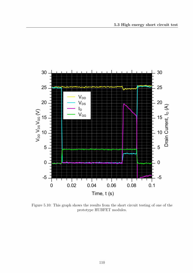
5.3 High energy short circuit test
VDD V
DS VGG (V)
-5
0
5
10
15
20
25
30
Drain Current, ID (A)
-5
0
5
10
15
20
25
30
Time, t (s)
0 0.02 0.04 0.06 0.08 0.1
VDDVDSIDVGG
Figure 5.10: This graph shows the results from the short circuit testing of one of theprototype HUBFET modules.
110
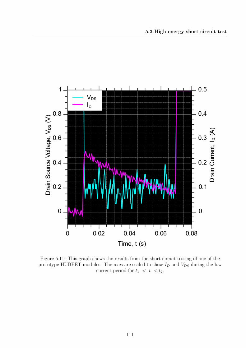
5.3 High energy short circuit test
Drain Source Voltage, VDS (V)
0
0.2
0.4
0.6
0.8
1
Drain Current, ID (A)
0
0.1
0.2
0.3
0.4
0.5
Time, t (s)
0 0.02 0.04 0.06 0.08
VDSID
Figure 5.11: This graph shows the results from the short circuit testing of one of theprototype HUBFET modules. The axes are scaled to show ID and VDS during the low
current period for t1 < t < t2.
111

5.4 Analysis
5.4 Analysis
The results of the IV and short circuit test from this chapter show all three tested devices be-
having as would be expected. Figure 5.12 shows the instantaneous power loss for MOSFET,
IGBT and HUBFET during the low current phase of the short circuit test.
The power loss values for the IGBT and MOSFET shown in figures 5.12 and 5.13 and
in Table 5.3 are the average of the three tested devices. It should be noted that the IGBT
and MOSFET are both in commercial packaging and will have more efficient thermal man-
agement than the HUBFET, which is on a test mounting. We can see that during the low
current phase of the short circuit test the MOSFET loses the least power, the IGBT loses
the most and the HUBFET falls in between, but is significantly closer to the MOSFET in
terms of power loss. During the high current phase, the MOSFET loses the most energy,
the IGBT the least and the HUBFET is in between again, but this time its power loss is
closer in value to the IGBT. A summary of these results can be found in Table 5.3. During
the short circuit test, the only change in the circuit between the nominal and short circuit
phases is the load. The gate signal to the devices was not changed until it was time to turn
off the switches. This shows the unique advantage of the HUBFET in that during a surge
condition, the surge itself causes the transition to bipolar mode. If the current in the circuit
increases due to a reduction in the resistance of the load and the HUBFET is operating
in unipolar mode then the response of the HUBFET will initially be linear. In accordance
with Kirchoff’s Voltage Law when the load resistance reduces but the supply voltage to the
network remains the same, the unipolar RDS(on) of the HUBFET will become a larger pro-
portion of the resistance of the network and the voltage dropped across it will necessarily
112
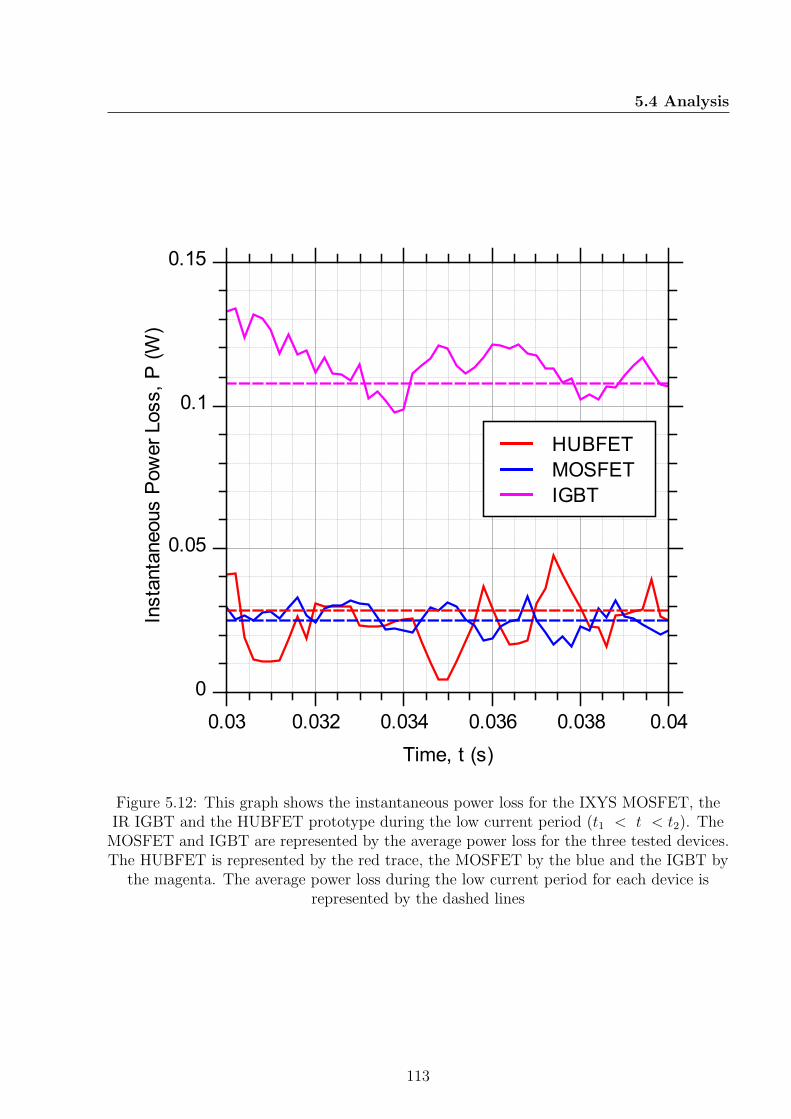
5.4 Analysis
Instantaneous Power Loss, P (W)
0
0.05
0.1
0.15
Time, t (s)
0.03 0.032 0.034 0.036 0.038 0.04
HUBFET
MOSFET
IGBT
Figure 5.12: This graph shows the instantaneous power loss for the IXYS MOSFET, theIR IGBT and the HUBFET prototype during the low current period (t1 < t < t2). TheMOSFET and IGBT are represented by the average power loss for the three tested devices.The HUBFET is represented by the red trace, the MOSFET by the blue and the IGBT by
the magenta. The average power loss during the low current period for each device isrepresented by the dashed lines
113
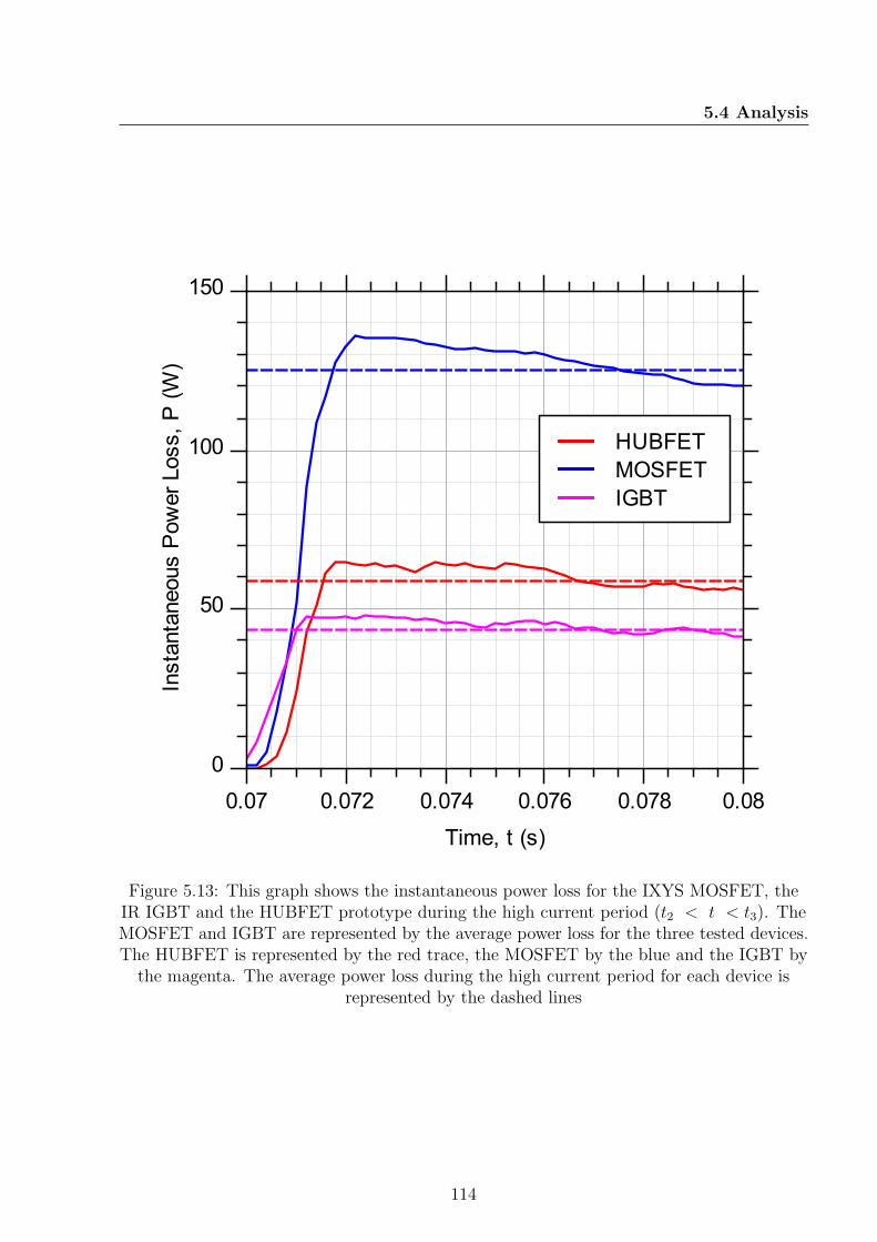
5.4 Analysis
Instantaneous Power Loss, P (W)
0
50
100
150
Time, t (s)
0.07 0.072 0.074 0.076 0.078 0.08
HUBFET
MOSFET
IGBT
Figure 5.13: This graph shows the instantaneous power loss for the IXYS MOSFET, theIR IGBT and the HUBFET prototype during the high current period (t2 < t < t3). TheMOSFET and IGBT are represented by the average power loss for the three tested devices.The HUBFET is represented by the red trace, the MOSFET by the blue and the IGBT by
the magenta. The average power loss during the high current period for each device isrepresented by the dashed lines
114

5.5 Summary
Table 5.3: This table shows the average instantaneous power loss for the IXYS MOSFET,IR IGBT and HUBFET during the low current and high current phases of the short circuit
test.
DevicePloss (W.cm−2)low current
Ploss (W.cm−2)high current
HUBFET 0.029 59
MOSFET 0.025 125
IGBT 0.108 43
increase. When this voltage reaches Vk the HUBFET enters bipolar mode. This allows it
to conduct a higher current at a lower voltage than the MOSFET during the short circuit.
This results in the lower power loss seen in Figure 5.13 and in Table 5.3.
5.5 Summary
In this Chapter it has been shown that the HUBFET described through simulations in
Chapter 4 is feasible to fabricate using modern processing techniques. It also behaves exactly
as predicted by simulation and fits the application for which it was originally envisaged.
The HUBFET modules tested in this Chapter are unoptimised proof of concept test pieces.
Specifically with regards to the drain implants that give the HUBFET its unique on-state
characteristic. These modules were fabricated using a mask set designed for a different
process. This suggests that changes could be made to the HUBFET design in order to
improve its on-state characteristics such as reducing RDS(on) and Vk. In Chapter 6 changes
to the pattern of implants at the drain of the device will be investigated in order to improve
its on-state performance. This will include the size and shape of the pattern, as well as the
115

5.5 Summary
ratio of N+ area to P+ area. The on-state analysis of the the HUBFET from this chapter
was presented by the author at APEC 2012 [67].
116

Chapter
6Analysis of the HUBFET drain
implant pattern
In this chapter the pattern of implants at the drain of the HUBFET and how this pattern
influences the device’s on-state characteristics will be investigated. First, 2D finite element
simulations will be used to show that the drain implant structure of the HUBFET affects the
on-state resistance and bipolar knee voltage of the device. This effect is then investigated
further through the fabrication of silicon test structures. The motivation for fabricating the
test parts will be discussed and the methods used for fabrication will be described. Finally,
the results of the simulations and physical testing will be analysed and summarised. Further
details on the work completed for this chapter can be found in appendicies A, B and C.
6.1 Simulation
In Chapter 5 the princliples of the HUBFET concept were demonstrated using proof of
concept devices manufactured for this project by ABB. The devices were fabricated using an
existing mask set that had been developed and optimised for the BIGT (see Chapter 3) to
117

6.1 Simulation
give the best performance of the integrated PIN diode for inductive switching applications.
In this section 2D finite element simulations similar to those seen in Chapter 4 are used to
determine how the different parameters used to fabricate the drain structure of the HUBFET
change its on-state performance. Specifically, the aim is to reduce RDS(on) and Vk as much
as possible whilst retaining a strong bipolar action at higher currents. The parameters that
will be considered are the ratio of N+ to P+ doping at the drain contact and the absolute
dimensions of the implants.
6.1.1 Method
The finite element simulations used in this section were performed using the Silvaco software
suite. The devices were built in the DevEdit strucure editor and simulated in the Atlas
device simulator.
Gate structure removal
It was decided that, in order to simplify the simulations so as to allow the work to be
completed in a reasonable time frame, the gate structure should be removed from the models.
This significantly reduces the number of nodes in the simulation as the region around the
channel requires a very fine mesh in order to converge and produce an accurate result. A
fine mesh involves more nodes and therefore more computation steps. For large simulations,
such as those required for the HUBFET, this can result in simulations taking several days to
converge and produce a useful result. For developing a design using many iterative steps this
quickly becomes impractical. As it is the on-state characteristic rather than the switching
118

6.1 Simulation
performance of the HUBFET that is critical to this investigation, the gate structure is not
necessary for the simulation results to be considered valid. The silicon MOS gate is a well
understood structure and has been extremely well optimised for commercial processes. The
area of interest in the HUBFET structure is at the drain terminal of the device which, for
the purpose of optimisation, is independent of the gate structure. The largest contributor
to RDS(on) in a silicon power MOSFET is from the drift region resistance (RD) as seen in
Equation 3.1 and Figure 3.4 in Chapter 3. The higher the breakdown voltage (VBR) of
the device, the wider and more lightly doped the drift region becomes which increases the
dominance of RD in the current path. The simulations used in this section will therefore
simply consist of the drift region and the drain structure, with the gate structure removed
and replaced by a single large source contact as seen in Figure 6.1. The HUBFET is a
MOSFET in parallel with an IGBT, this modified structure is effectively a PiN diode in
parallel with a resistor. This structure has the same forward characteristic as a parallel
MOSFET and IGBT in the on-state.
Simulation parameters
In Table 6.1 and Figure 6.2 the parameters for the simulations are shown. Dimensions b, c
and d are listed as variable as they change between the simulated structures. For this work
b will be either 2000 µm, 1000 µm, 500 µm or 250 µm. This represents 1, 2, 4 and 8 celled
structures at the drain contact. Dimensions c and d vary as a proportion of b. c+ d = b for
all cases and Nb = a where N is the number of drain cells. To see the impact of changing
the proportion of N+ to P+ the ratio of c : d was changed between 100 : 0, 80 : 20, 50 : 50,
119

6.1 Simulation
Source Source
Drain
Gate
N- drift
N+ P+
Source
Drain
N- drift
N+ P+
Figure 6.1: This diagram shows the method used to alter the HUBFET design making itsuitable for simulating the drain structure. The gate is removed and replaced with a single
source contact.
20 : 80 and 0 : 100. The ratios of 100 : 0 and 0 : 100 represent the structure of a pure
MOSFET and IGBT respectively. Basic schematic diagrams of all the structures used in
simulation are shown in figures 6.3 - 6.5. Table 6.2 summarises the properties of each of
the structures, as well as the value of the variables b, c and d as shown in Table 6.1 and
Figure 6.1. The variable d can also be considered as the width of the P+ drain implants
(WP+).
6.1.2 Results
In this section the results from the 2D finite element simulations are presented. 14 simula-
tions were performed with a variety of drain patterns and the individual IV curves for each
simulation can be found in Appendix C. The parameters for the simulations are described
in Table 6.1 and Figures 6.2, 6.3, 6.4 and 6.5. The extracted values for RDS(on) and Vk are
summarised in Table 6.2. Two parameters were varied to analyse how they affect on the
120

6.1 Simulation
Table 6.1: This table lists the values of the parameters for the 2D drain simulations asshown in Figure 6.2
Label Description Value
a Simulation width 2000 µm
b Drain cell width variable
c N+ implant width variable
d P+ implant width variable
e Drift region thickness 110 µm
f N+/P+ implant depth 1 µm
A Drift region doping (Arsenic) 1.43 × 1014 cm−3
B N+ doping (Phosphorus) 1.00 × 1020 cm−3
C P+ doping (Boron) 5.00 × 1019 cm−3
on-state characteristic of the HUBFET. These parameters are the N : P doping ratio at the
drain contact and the number of cells at the same contact. All other parameters were kept
the same so that only the pattern variation would influence the simulation output. First the
impact of the pattern on RDS(on) will be presented followed by how the same changes affect
Vk.
Unipolar on-state resistance
Here The way the pattern changes RDS(on) is presented. First the impact of the N : P ratio
is considered followed by the effect of varying the number of cells.
• Ratio The ratio of N+ to P+ doping at the drain of the HUBFET has a clear impact
on the results of the simulations. The higher the proportion of N+, the lower RDS(on)
becomes. This can be seen in Figures 6.6, 6.7 and 6.8. Here it is clear that in general
the N : P 80 : 20 devices (Sim 11, Sim 12, Sim 13 and Sim 14) have the lowest RDS(on).
121

6.1 Simulation
B
A
C
Source
Drain
a
b
c d
e
f
Figure 6.2: This diagram shows the structure used for the simulations in this chapter. Thelabelled parameter values can be found in tables 6.1 and 6.2
The least resistive being device Sim 14 where RDS(on)sp = 0.355 Ω.cm2. This is only
marginally higher than the resistance of the N : P 100 : 0 MOSFET device (Sim 01)
for which RDS(on)sp = 0.339 Ω.cm2. As the amount of P+ relative to N+ increases,
so does RDS(on). This can be seen in the results for the N : P 50 : 50 and 20 : 80 devices
in Table 6.2 and figures 6.6 and 6.7.
• Number of cells Figures 6.6, 6.7 and 6.8 also show a trend in the way the number
of cells affects RDS(on). For each of the ratios, the device with the lowest RDS(on) is
the device with the highest number of cells. As the number of cells decreases, RDS(on)
increases. This effect is a result of the width of the P+ regions (WP+) and will be
analysed in Section 6.3.1.
122
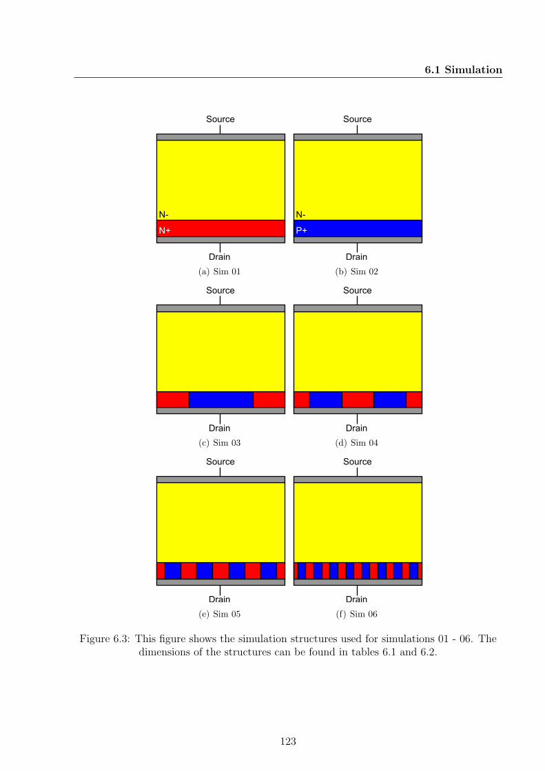
6.1 Simulation
Source
Drain
N-
N+
(a) Sim 01
Source
Drain
N-
P+
(b) Sim 02
Source
Drain
(c) Sim 03
Source
Drain
(d) Sim 04
Source
Drain
(e) Sim 05
Source
Drain
(f) Sim 06
Figure 6.3: This figure shows the simulation structures used for simulations 01 - 06. Thedimensions of the structures can be found in tables 6.1 and 6.2.
123
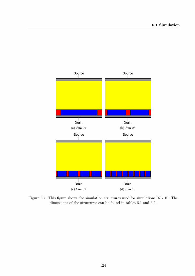
6.1 Simulation
Source
Drain
(a) Sim 07
Source
Drain
(b) Sim 08
Source
Drain
(c) Sim 09
Source
Drain
(d) Sim 10
Figure 6.4: This figure shows the simulation structures used for simulations 07 - 10. Thedimensions of the structures can be found in tables 6.1 and 6.2.
124
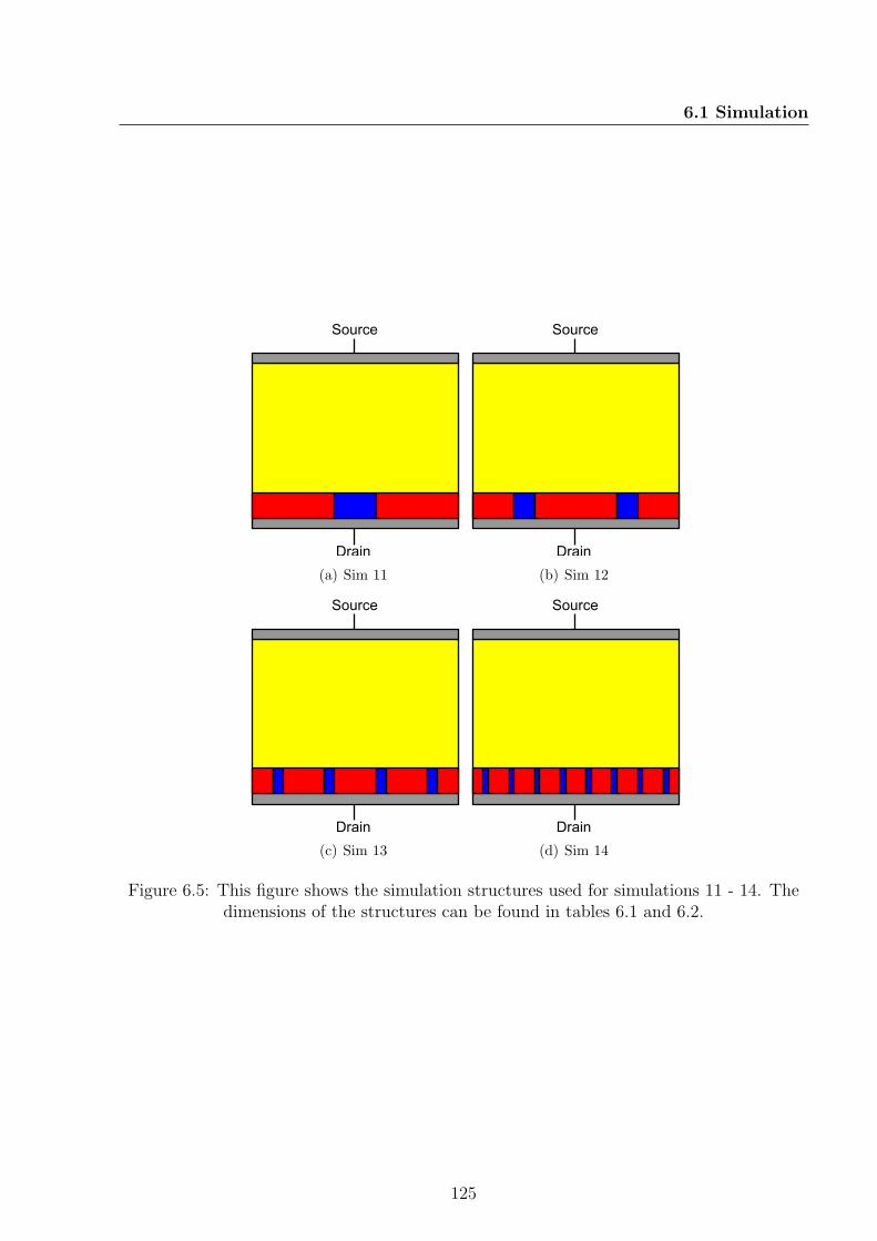
6.1 Simulation
Source
Drain
(a) Sim 11
Source
Drain
(b) Sim 12
Source
Drain
(c) Sim 13
Source
Drain
(d) Sim 14
Figure 6.5: This figure shows the simulation structures used for simulations 11 - 14. Thedimensions of the structures can be found in tables 6.1 and 6.2.
125
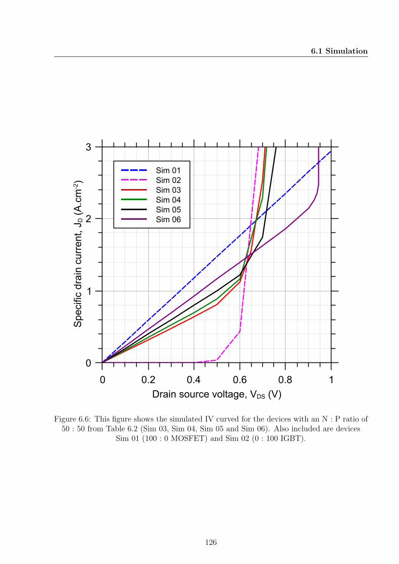
6.1 Simulation
Specific drain current, JD (A.cm
-2)
0
1
2
3
Drain source voltage, VDS (V)
0 0.2 0.4 0.6 0.8 1
Sim 01
Sim 02
Sim 03
Sim 04
Sim 05
Sim 06
Figure 6.6: This figure shows the simulated IV curved for the devices with an N : P ratio of50 : 50 from Table 6.2 (Sim 03, Sim 04, Sim 05 and Sim 06). Also included are devices
Sim 01 (100 : 0 MOSFET) and Sim 02 (0 : 100 IGBT).
126
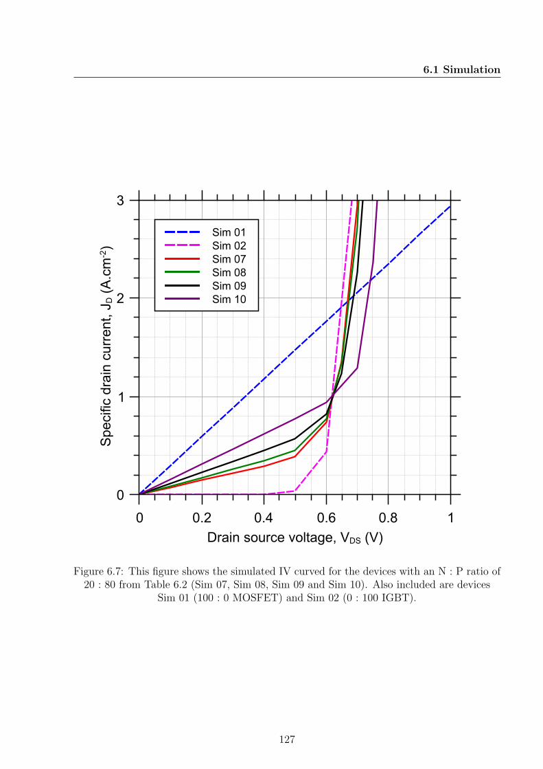
6.1 Simulation
Specific drain current, JD (A.cm
-2)
0
1
2
3
Drain source voltage, VDS (V)
0 0.2 0.4 0.6 0.8 1
Sim 01
Sim 02
Sim 07
Sim 08
Sim 09
Sim 10
Figure 6.7: This figure shows the simulated IV curved for the devices with an N : P ratio of20 : 80 from Table 6.2 (Sim 07, Sim 08, Sim 09 and Sim 10). Also included are devices
Sim 01 (100 : 0 MOSFET) and Sim 02 (0 : 100 IGBT).
127
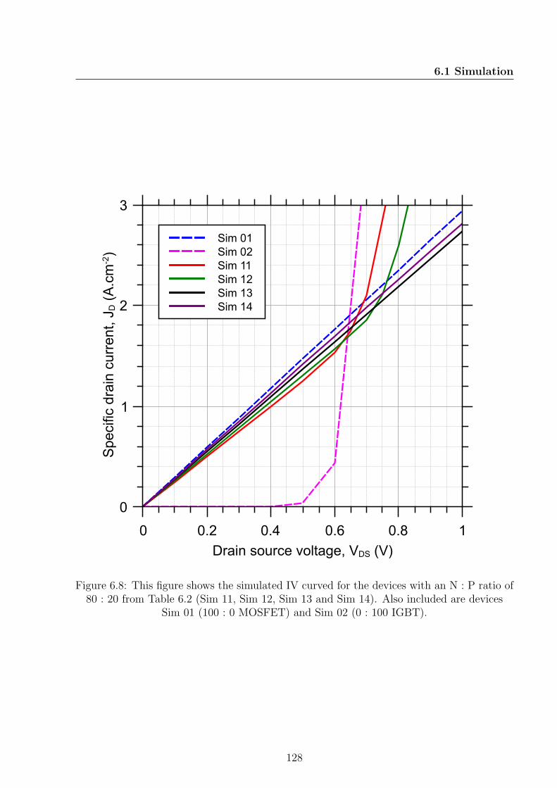
6.1 Simulation
Specific drain current, JD (A.cm
-2)
0
1
2
3
Drain source voltage, VDS (V)
0 0.2 0.4 0.6 0.8 1
Sim 01
Sim 02
Sim 11
Sim 12
Sim 13
Sim 14
Figure 6.8: This figure shows the simulated IV curved for the devices with an N : P ratio of80 : 20 from Table 6.2 (Sim 11, Sim 12, Sim 13 and Sim 14). Also included are devices
Sim 01 (100 : 0 MOSFET) and Sim 02 (0 : 100 IGBT).
128

6.1 Simulation
Table 6.2: This table lists the values of the variables from Table 6.1 used in the 2D drainsimulations as shown in Figures 6.2, 6.3, 6.4 and 6.5
Label N : P ratio Cells b c d RDS(on)sp. Vk
Sim 01 100 : 0 1 2000 µm 2000 µm - 0.339 Ω.cm2 -
Sim 02 0 : 100 1 2000 µm - 2000 µm - 0.4 V
Sim 03 50 : 50 1 2000 µm 1000 µm 1000 µm 0.630 Ω.cm2 0.5 V
Sim 04 50 : 50 2 1000 µm 500 µm 500 µm 0.574 Ω.cm2 0.5 V
Sim 05 50 : 50 4 500 µm 250 µm 250 µm 0.502 Ω.cm2 0.6 V
Sim 06 50 : 50 8 250 µm 125 µm 125 µm 0.431 Ω.cm2 0.9 V
Sim 07 20 : 80 1 2000 µm 400 µm 1600 µm 1.381 Ω.cm2 0.5 V
Sim 08 20 : 80 2 1000 µm 200 µm 800 µm 1.164 Ω.cm2 0.5 V
Sim 09 20 : 80 4 500 µm 100 µm 400 µm 0.893 Ω.cm2 0.5 V
Sim 10 20 : 80 8 250 µm 50 µm 200 µm 0.649 Ω.cm2 0.6 V
Sim 11 80 : 20 1 2000 µm 1600 µm 400 µm 0.401 Ω.cm2 0.5 V
Sim 12 80 : 20 2 1000 µm 800 µm 200 µm 0.384 Ω.cm2 0.7 V
Sim 13 80 : 20 4 500 µm 400 µm 100 µm 0.366 Ω.cm2 1.1 V
Sim 14 80 : 20 8 250 µm 200 µm 50 µm 0.354 Ω.cm2 1.9 V
These results will be analysed in Section 6.3 where they will be compared with results
gathered experimentally from physical test devices.
Bipolar knee voltage
The ratio of N+ to P+ doping and the number of repeated cells do not of themselves influence
Vk. However, the dimension of the P+ implants does. Figure 6.9 shows the relationship
between the width of the P+ regions (WP+, dimension d from Figure 6.2 and Table 6.2) and
Vk. In this figure it can clearly be seen that Vk increases as WP+ decreases with Vk getting
exponentially larger as WP+ approaches zero. This effect will be fully analysed in Section 6.3
after the results of the fabrication work have been presented.
129
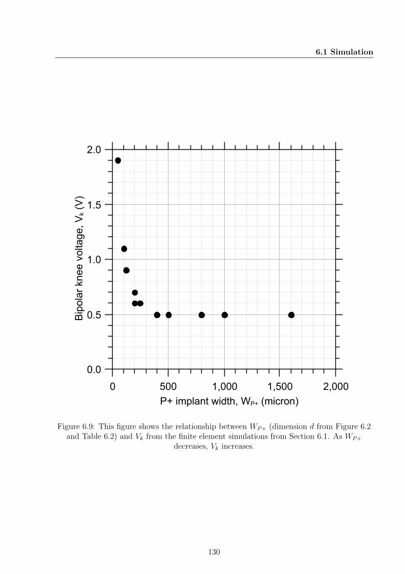
6.1 Simulation
Bipolar knee voltage, Vk (V)
0.0
0.5
1.0
1.5
2.0
P+ implant width, WP+ (micron)
0 500 1,000 1,500 2,000
Figure 6.9: This figure shows the relationship between WP+ (dimension d from Figure 6.2and Table 6.2) and Vk from the finite element simulations from Section 6.1. As WP+
decreases, Vk increases.
130

6.2 Fabrication
Summary
These simulations show several interesting characteristics which will be investigated further
in the next section through fabrication. However, it is clear that RDS(on) is influenced by
both the ratio of N+ to P+ implants at the drain contact and by WP+.
6.2 Fabrication
The results of the 2D simulations shown in figures 6.6, 6.7 and 6.8 from the previous section
show that variations in the drain structure of the HUBFET have a considerable effect on
the on-state characteristics of the device. However, it may be that these simulations do not
show the complete picture. When Storasta et al. were investigating the pattern of implants
to be used to integrate a PiN diode into the collector terminal of an IGBT [30] they showed
that it is not sufficient to simply carry out 2D simulations of the device structure as there are
additional effects that only become apparent in full 3D devices. Therefore it is necessary to
investigate how the complete pattern of implants at the drain of the HUBFET changes the
way the device behaves. Initially, further finite element simulations were considered for this
task in addition to those seen in the previous section. A full 2D pattern of implants giving
rise to a 3D simulation would be required. Unfortunately the computation power required
to run this type of simulation in a reasonable time frame was too great for the facilities
available so it was decided to fabricate physical test parts instead. The design, fabrication
and measurement of these parts are described in this section.
131

6.2 Fabrication
6.2.1 Method
Test structure design
In order to maximise the useful results from this fabrication work it was decided to keep
the test parts as simple as possible. As was the case with simulations from Section 6.1, this
means removing the gate structure from the design. This process is shown in Figure 6.10.
The test structures are fabricated on silicon epi wafers with the drain contact on the top
side and the source contact on the backside. The whole structure has therefore been flipped
over. The highly doped substrate wafer replaces the gate structure with the epitaxial layer
forming the drift region and the drain structure is implanted into the topside.
Rotate 180o
Source Source
SourceDrain
Drain
Gate
N- drift
N- drift
N+ P+
N+ Substrate
N+ P+
Figure 6.10: This diagram shows the method used to alter the HUBFET design making itsuitable for fabrication in order to test the drain structure.
This method allows for a much simpler fabrication process and eliminates the need to
handle the ultra thin wafers that were used in the commercial process to build the devices
tested in Chapter 5. Therefore the results from this fabrication work are only valid for the
132

6.2 Fabrication
forward on-state characteristics of the HUBFET. This method can be used, as it could for the
simulations from the previous section, because it is well established that, in higher voltage
unipolar silicon power devices, the largest component of the total RDS(on) is the drift region
resistance. This means that when the device is on, the channel and contact resistances are
not critical parameters. Taking this approach allows a large number of designs to be tested
without a complicated and potentially error prone fabrication process.
Implant Patterns
In order to investigate how changes in the pattern of the drain implants affect the on-state
characteristic of the HUBFET, three key aspects of the implant design were investigated.
• The geometric shape of the implants. It was shown by Storasta et al. in [30]
that the shape of the implants at the collector of the BIGT has a significant influence
on the on-state and switching characteristic of the device. Therefore for this work,
the geometric pattern of implants was analysed using three different shapes (stripes,
squares and circles) as seen in Figure 6.11.
N+
P+
Figure 6.11: This diagram shows the three patterns used to test the drain structure:squares, circles and stripes. The N+ regions are represented by the colour red and the P+
regions by blue.
133

6.2 Fabrication
• The ratio of the area of N+ implants to P+ implants. It was shown in the 2D
simulations from the previous section that the ratio of the length of the N+ and P+
implants at the drain contact has a significant impact on the on-state characteristics
of the HUBFET, particularly RDS(on)sp. This relationship will be investigated to see
how it translates into three dimensions. For simplicity only three N:P area ratios were
considered (80 : 20, 50 : 50 and 20 : 80) as well as 100 % N (pure MOSFET) and 100 %
P (pure IGBT). Single square examples of these can be seen in Figure 6.12.
N:P - 80:20 N:P - 50:50 N:P - 20:80
N:P - 100:0 N:P - 0:100
Figure 6.12: This diagram shows the five area ratios used to test the drain structure. TheN+ regions are represented by the colour red and the P+ regions by blue. All of these
examples are the single square of P design.
• The size of the P+ implants. Also indicated by the simulations was that the size of
the P+ implants changes both Vk and RDS(on). These effects will also be investigated.
Figure 6.13 shows how the size of the implants can be varied whilst maintaining the
same shape and N : P area ratio. This will be investigated with four different sized
134

6.2 Fabrication
implants for the square and circular patterns (1, 4, 16 and 64 implanted regions). For
the striped pattern there will be five variations (1, 2, 4, 8 and 16 pairs of stripes).
Figure 6.13: This diagram shows how the size of the implanted areas at the drain structurewas varied whilst maintaining the same shape and N : P area ratio. The implant areas (in
this case squares) are divided up, maintaining the same area ratio, but reducing theindividual implant size. The N+ regions are represented by the colour red and the P+
regions by blue.
Mask layer design
A four mask process was designed in order to fabricate these test devices so that they could be
studied. The master view of the wafer layout can be seen in Figure 6.14 and in Appendix A.
Table 6.4 lists all of the different options fabricated along with some of their key measured
parameters. The mask designs used to fabricate each of these devices can also be found in
Appendix A. Each shape was tested at the three area ratios and each of those in turn was
tested for different sized P+ implants. For several of the devices to be fabricated, there were
two ways to produce the implant pattern so it would meet the specification. For example
in Figure 6.15 it is clear that if the N+ to P+ area ratio is 50 : 50 then this can be created
through either islands of P+ surrounded by N+ or islands of N+ surrounded by P+. In
this case it is single squares. For all patterns with this issue, both options were fabricated.
The available facilities dictated that the test parts be fabricated on a 3 in (75 mm) silicon
135

6.2 Fabrication
wafer. In order to balance a reasonable feature size, large enough for probing to, and a small
enough device such that a reasonable number of repetitions could be made for each design.
It was decided to use a 2× 2 mm2 active area for each device. Figure 6.16 shows the basic
format for all of the test parts. Appendix A contains a schematic of each of the master GDS
files used to create the masks for each of the designed test devices.
On each quarter wafer each device was repeated 3 times (giving a total 12 repetitions
across the whole wafer), except in the case where there were two ways to design the device
(as described above) where the two options were repeated twice each (making a total of
8 repetition for each across the wafer). In total, 57 different designs were fabricated and
were repeated a minimum of 8 times each across the whole wafer. The masks for these
devices were designed using Tanner Tools L-Edit software. The four masks can be seen in
Appendix A and they are:
• Alignment marks and MESA. This mask includes the alignment patterns and the
MESA structures which provide isolation between devices (Figure A.2).
• N+ implant. This mask provides the shape for the N+ implants (Figure A.3).
• P+ implant. This mask provides the shape for the P+ implants (Figure A.4).
• Metal. This mask provides the shape for the topside metal layer and physical device
labels (Figure A.5).
Figure 6.17 shows how the device is built up using the four masks.
136
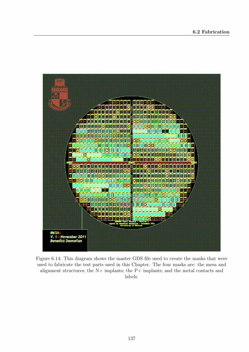
6.2 Fabrication
Figure 6.14: This diagram shows the master GDS file used to create the masks that wereused to fabricate the test parts used in this Chapter. The four masks are: the mesa andalignment structures; the N+ implants; the P+ implants; and the metal contacts and
labels.
137
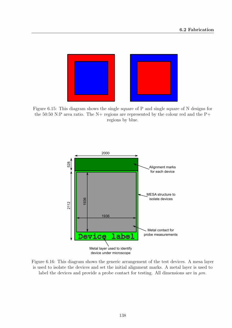
6.2 Fabrication
Figure 6.15: This diagram shows the single square of P and single square of N designs forthe 50:50 N:P area ratio. The N+ regions are represented by the colour red and the P+
regions by blue.
Device label
2000
2112
1936
19
36
528
Metal layer used to identify
device under microscope
Metal contact for
probe measurements
MESA structure to
isolate devices
Alignment marks
for each device
Figure 6.16: This diagram shows the generic arrangement of the test devices. A mesa layeris used to isolate the devices and set the initial alignment marks. A metal layer is used to
label the devices and provide a probe contact for testing. All dimensions are in µm.
138
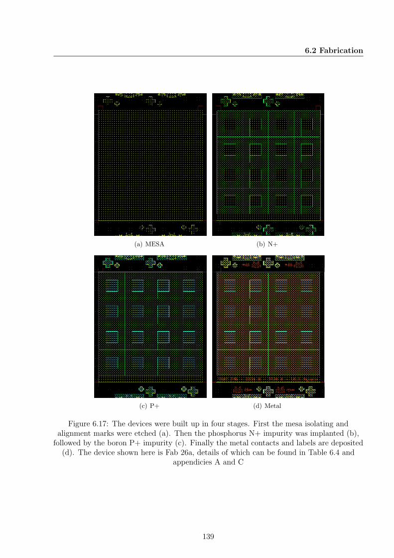
6.2 Fabrication
(a) MESA (b) N+
(c) P+ (d) Metal
Figure 6.17: The devices were built up in four stages. First the mesa isolating andalignment marks were etched (a). Then the phosphorus N+ impurity was implanted (b),
followed by the boron P+ impurity (c). Finally the metal contacts and labels are deposited(d). The device shown here is Fab 26a, details of which can be found in Table 6.4 and
appendicies A and C
139

6.2 Fabrication
Fabrication process
In this section the method used to fabricate the test pieces will briefly be described. Full
details of each of the fabrication process steps can be found in Appendix B. The test devices
were fabricated on a Si epi wafer obtained from CEMAT silicon in Poland. All the subsequent
fabrication steps were carried out in the Class 1000 Science City cleanroom facility at the
University of Warwick, UK, with the exception of the two implantation steps which were
carried out at Cutting Edge Ions LLC in California, USA. First a photoresist masking
layer was created using the Mesa and alignment mask. The pattern was etched into the
silicon using a vertical dry etch program in an ICP etcher to form the mesa isolation regions
and alignment structures. Next a thick, hard baked photoresist implant masking layer was
created using the N+ implant mask. The wafer was then sent to Cutting Edge Ions for the
phosphorus N+ implantation stage, the details of which are described in Table 6.3. After the
wafer was returned the photoresist layer was removed and the P+ implant mask was created
using more photoresist and the P+ implant mask. Again the wafer was sent for implantation,
this time a boron P+ implant and the details can be found in Table 6.3. Upon its return, the
photoresist was removed and the implants were annealed for 30 minutes at 1100 oC to diffuse
the dopants in a gaussian profile to a depth of approximately 1.5 − 2.0 µm. The implantation
stages were defined using Monte Carlo simulation lookup tables generated by SRIM software
to determine the energy required to implant to a depth of approximately 1 µm. The Silvaco
Athena Process simulator was then used to determine the required activation and drive in
anneal time to generate a gaussian implant distribution with a depth of 1.5 − 2.0 µm. The
1D doping profiles extracted from the software are shown in Figure 6.18 which shows the
140

6.2 Fabrication
Table 6.3: This table lists the values of the parameters for the implants used in thefabrication of the HUBFET drain pattern test parts
Parameter N+ Implant P+ Implant
Species Phosphorus Boron
Dose 5× 1015 cm−2 5× 1015 cm−2
Energy 150 keV 60 keV
Tilt 7o 7o
Implant depth 1 µm 0.9 µm
Anneal depth 1.5 µm 1.9 µm
dopant distribution before and after the anneal step. Using the metal mask and a bilayer lift
off process, the aluminium contacts were applied to the topside of the wafer and a blanket
layer of aluminium was applied to the backside using a sputterer. Finally the contacts were
annealed using the halogen lamps in the sputterer in a pure argon environment for 10 min
at 425 oC.
A photograph of the final wafer can be seen in Figure 6.19. A ₤ 1 coin is used as a size
comparison and a composite microscope image is also included to show two of the fabricated
devices.
Measurements
In this section the method of measurement used to extract the on-state data from the test
pieces is described. The equipment used was an Agilent B1500A Semiconductor Device
Analyser and a Wentworth Labs probe station. The devices were electrically grounded
through the chuck of the probe station which connected to the source contact on the backside
of the device. Each test part was then individually probed and an IV sweep was taken. A
141
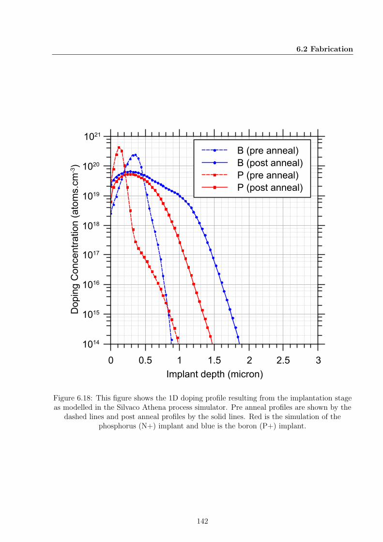
6.2 Fabrication
Doping Concentration (atoms.cm
-3)
1014
1015
1016
1017
1018
1019
1020
1021
Implant depth (micron)
0 0.5 1 1.5 2 2.5 3
B (pre anneal)
B (post anneal)
P (pre anneal)
P (post anneal)
Figure 6.18: This figure shows the 1D doping profile resulting from the implantation stageas modelled in the Silvaco Athena process simulator. Pre anneal profiles are shown by the
dashed lines and post anneal profiles by the solid lines. Red is the simulation of thephosphorus (N+) implant and blue is the boron (P+) implant.
142
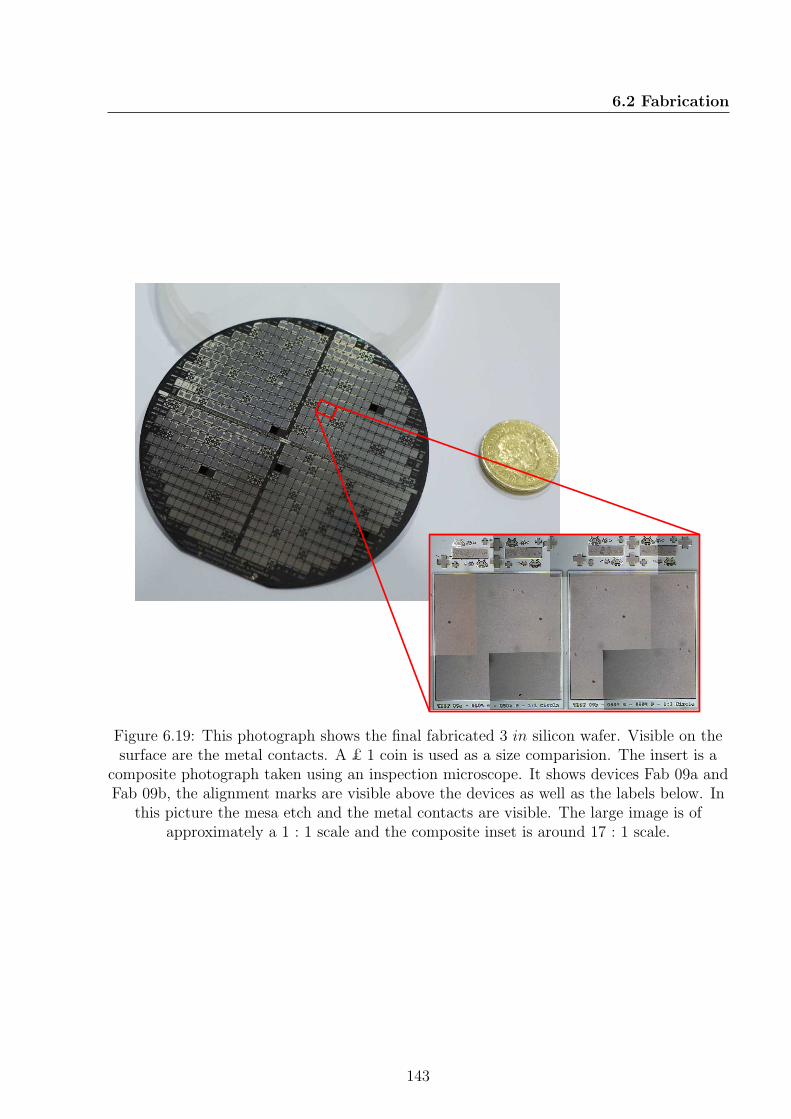
6.2 Fabrication
Figure 6.19: This photograph shows the final fabricated 3 in silicon wafer. Visible on thesurface are the metal contacts. A ₤ 1 coin is used as a size comparision. The insert is a
composite photograph taken using an inspection microscope. It shows devices Fab 09a andFab 09b, the alignment marks are visible above the devices as well as the labels below. In
this picture the mesa etch and the metal contacts are visible. The large image is ofapproximately a 1 : 1 scale and the composite inset is around 17 : 1 scale.
143

6.2 Fabrication
combination of the size of the test parts and the 100 mA current limit of the parameter
analyser limited the maximum current density during the measurements to 2.5 A.cm−2.
The voltage step resolution was also restricted to 8 steps per volt (0.125 V per step). The
measurements for all the repetitions of each design were collated and the mean and standard
deviation of the current for each voltage step was calculated. The uniformity was extremely
high with the maximum standard deviation for any point in the forward portion of the IV
curve not exceeding 0.03 A and the majority being less than 0.01 A. Full details are listed
in Table 6.4. The results from the measurements are discussed in the following section. The
plots and values referred to are the mean values for the collated results from the repetitions
of each device.
6.2.2 Results
In this section the results from the IV sweeps of the fabricated test parts are presented.
First, how each of the parameter variations affects RDS(on) will be shown followed by how
the same parameters change Vk.
Unipolar on-state resistance
• Size The size of the P+ implants has a moderate effect on RDS(on)sp. The larger the
P+ implant in equivalent devices (where all other parameters are constant) the higher
RDS(on)sp becomes. This can be seen in the comparison of devices shown in Figure 6.20.
Here device Fab 03 is compared with Fab 39. Both devices have a N : P area ratio of
50 : 50 made up from stripes. However device Fab 03 has one stripe of N+ and one
144
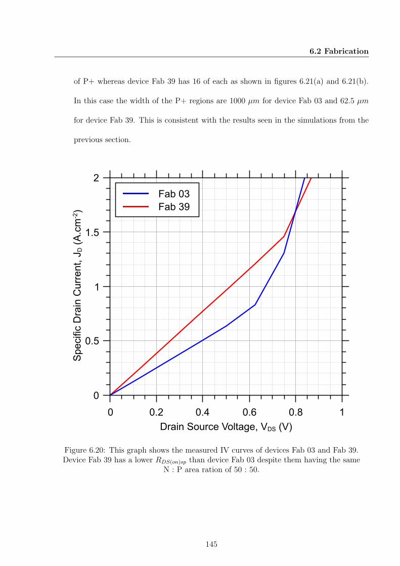
6.2 Fabrication
of P+ whereas device Fab 39 has 16 of each as shown in figures 6.21(a) and 6.21(b).
In this case the width of the P+ regions are 1000 µm for device Fab 03 and 62.5 µm
for device Fab 39. This is consistent with the results seen in the simulations from the
previous section.
Specific Drain Current, J
D (A.cm
-2)
0
0.5
1
1.5
2
Drain Source Voltage, VDS (V)
0 0.2 0.4 0.6 0.8 1
Fab 03
Fab 39
Figure 6.20: This graph shows the measured IV curves of devices Fab 03 and Fab 39.Device Fab 39 has a lower RDS(on)sp than device Fab 03 despite them having the same
N : P area ration of 50 : 50.
145

6.2 Fabrication
(a) Fab 03 (b) Fab 39
Figure 6.21: The implant pattern used at the drain contact of devices Fab 03 and Fab 39.Red represents N+ doping and blue represents P+ doping.
• Shape Variations in the shape of the implant appear to have little affect on RDS(on)sp.
The IV curves for each of the different pattern shapes are collated in figures 6.22, 6.23
and 6.24. It is clear from these graphs that there is no discernable relationship between
the shape of the pattern and RDS(on). In each case the curves are evenly distributed
with no obvious grouping. This is true for specific cases as well. Figure 6.33 shows a
comparison between devices Fab 03, Fab 06b and Fab 09b. These are all patterns with
an N : P area ratio of 50 : 50 consisting of a single area of P+ and a single area of N+.
Diagrams of each of the patterns can be found in figures 6.21(a), 6.25(a) and 6.25(b).
Despite the different patterns, the IV curves are all very similar with little variation in
RDS(on).
• Ratio The ratio of N : P implant area appears to be the most significant factor that
affects RDS(on)sp. In equivalent devices increasing the area of N+ doping compared to
P+ will reduce RDS(on)sp. This can be seen clearly in figures 6.26, 6.27 and 6.28. Each
figure shows the collated IV curves for each of the area ratios (80 : 20, 50 : 50 and
146
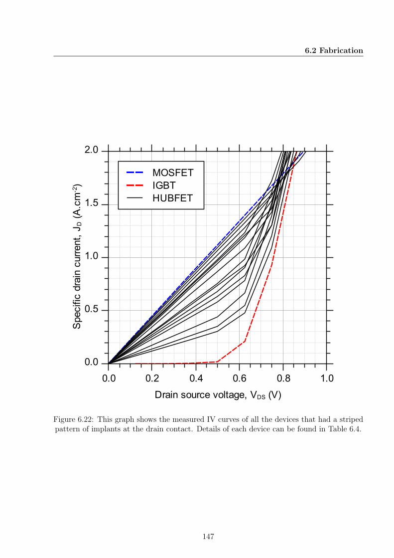
6.2 Fabrication
Specific drain current, J
D (A.cm
-2)
0.0
0.5
1.0
1.5
2.0
Drain source voltage, VDS (V)
0.0 0.2 0.4 0.6 0.8 1.0
MOSFET
IGBT
HUBFET
Figure 6.22: This graph shows the measured IV curves of all the devices that had a stripedpattern of implants at the drain contact. Details of each device can be found in Table 6.4.
147
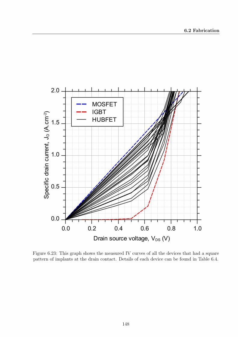
6.2 Fabrication
Specific drain current, J
D (A.cm
-2)
0.0
0.5
1.0
1.5
2.0
Drain source voltage, VDS (V)
0.0 0.2 0.4 0.6 0.8 1.0
MOSFET
IGBT
HUBFET
Figure 6.23: This graph shows the measured IV curves of all the devices that had a squarepattern of implants at the drain contact. Details of each device can be found in Table 6.4.
148
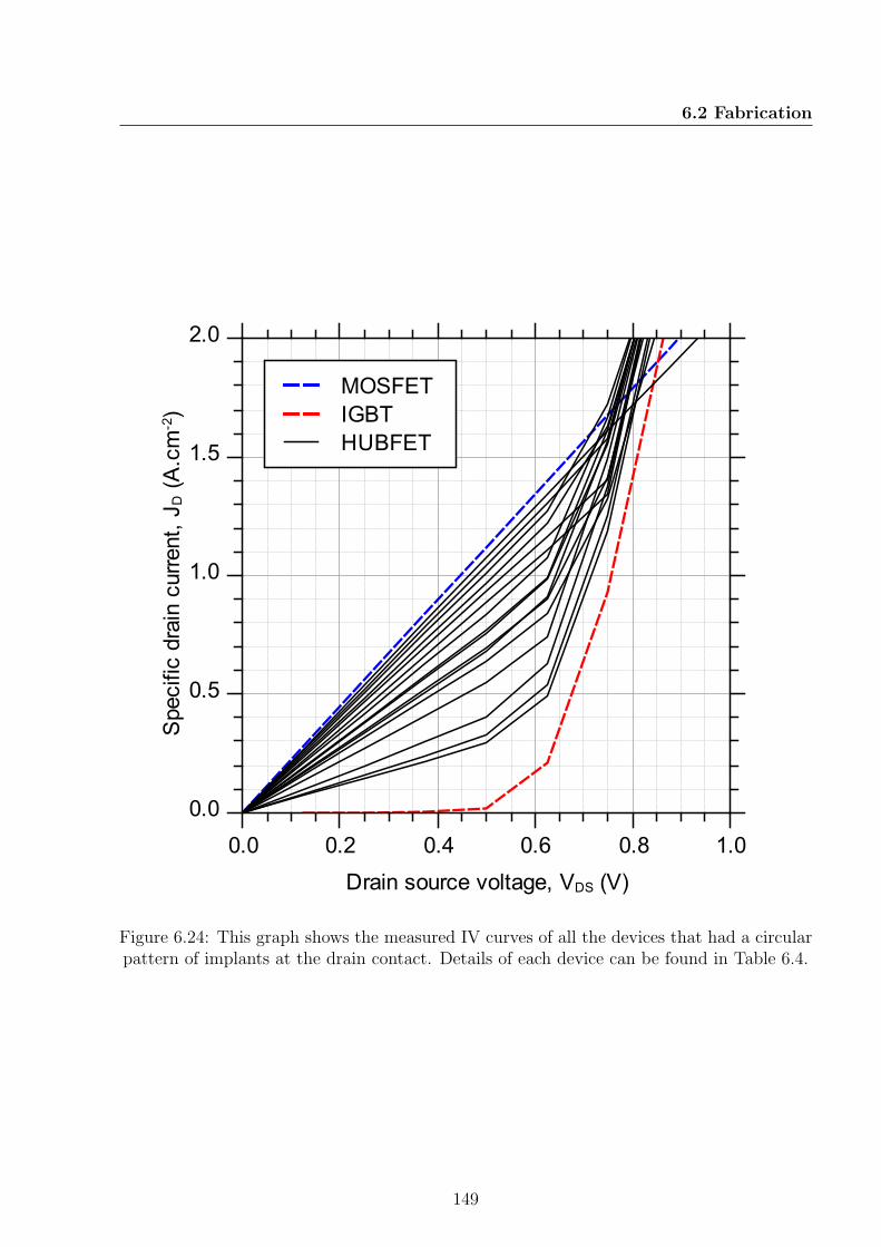
6.2 Fabrication
Specific drain current, J
D (A.cm
-2)
0.0
0.5
1.0
1.5
2.0
Drain source voltage, VDS (V)
0.0 0.2 0.4 0.6 0.8 1.0
MOSFET
IGBT
HUBFET
Figure 6.24: This graph shows the measured IV curves of all the devices that had a circularpattern of implants at the drain contact. Details of each device can be found in Table 6.4.
149

6.2 Fabrication
(a) Fab 06b (b) Fab 09b
Figure 6.25: The implant pattern used at the drain contact of devices Fab 06b andFab 09b. Red represents N+ doping and blue represents P+ doping.
20 : 80) as well as the 100 : 0 and 0 : 100 (MOSFET and IGBT) curves for comparison.
Clearly the different area ratios are grouped together with the higher proportion of N+
leading to a decrease in RDS(on). In the 80 : 20 N : P case, the best devices approach
the RDS(on) of the pure MOSFET. Again, this is consistent with the simulations.
From these results, it can be seen that the patterns leading to the lowest RDS(on) are those
with the highest proportion of N+ at the drain combined with the smallest P+ implants.
The lowest RDS(on) is found in devices Fab 35a, Fab 35b, Fab 38 and Fab 41. These devices
each have an N : P area ratio of 80 : 20 and have the smallest P+ implants of their shape.
The details of each device can be seen in Table 6.4 and Figure 6.29. These results are also
consistent with the simulations from Section 6.1. The analysis of why this is the case can
be found in Section 6.3 of this chapter.
150
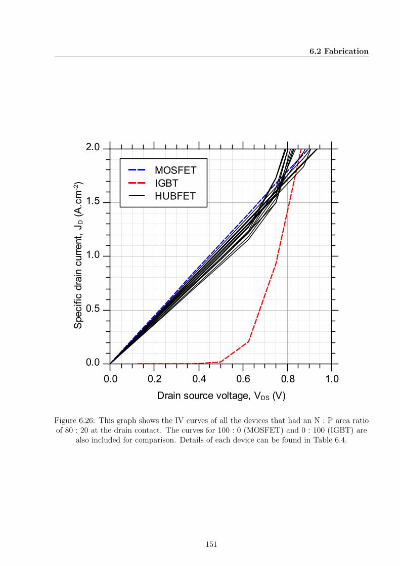
6.2 Fabrication
Specific drain current, J
D (A.cm
-2)
0.0
0.5
1.0
1.5
2.0
Drain source voltage, VDS (V)
0.0 0.2 0.4 0.6 0.8 1.0
MOSFET
IGBT
HUBFET
Figure 6.26: This graph shows the IV curves of all the devices that had an N : P area ratioof 80 : 20 at the drain contact. The curves for 100 : 0 (MOSFET) and 0 : 100 (IGBT) are
also included for comparison. Details of each device can be found in Table 6.4.
151
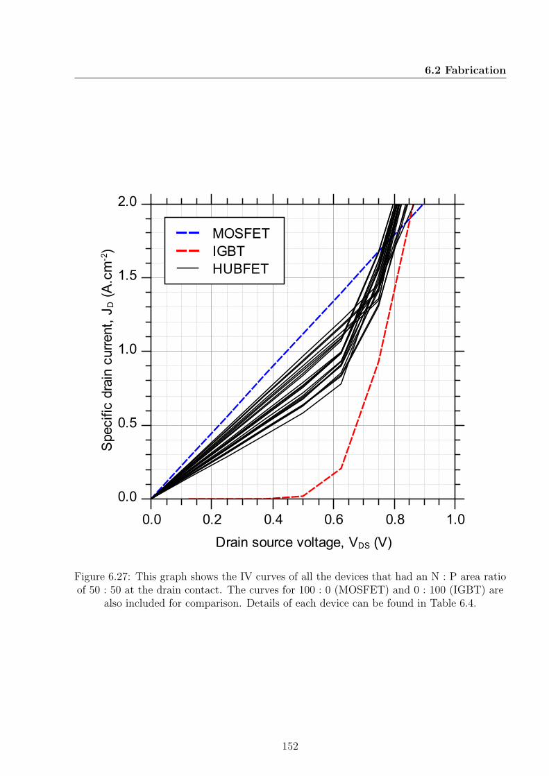
6.2 Fabrication
Specific drain current, J
D (A.cm
-2)
0.0
0.5
1.0
1.5
2.0
Drain source voltage, VDS (V)
0.0 0.2 0.4 0.6 0.8 1.0
MOSFET
IGBT
HUBFET
Figure 6.27: This graph shows the IV curves of all the devices that had an N : P area ratioof 50 : 50 at the drain contact. The curves for 100 : 0 (MOSFET) and 0 : 100 (IGBT) are
also included for comparison. Details of each device can be found in Table 6.4.
152
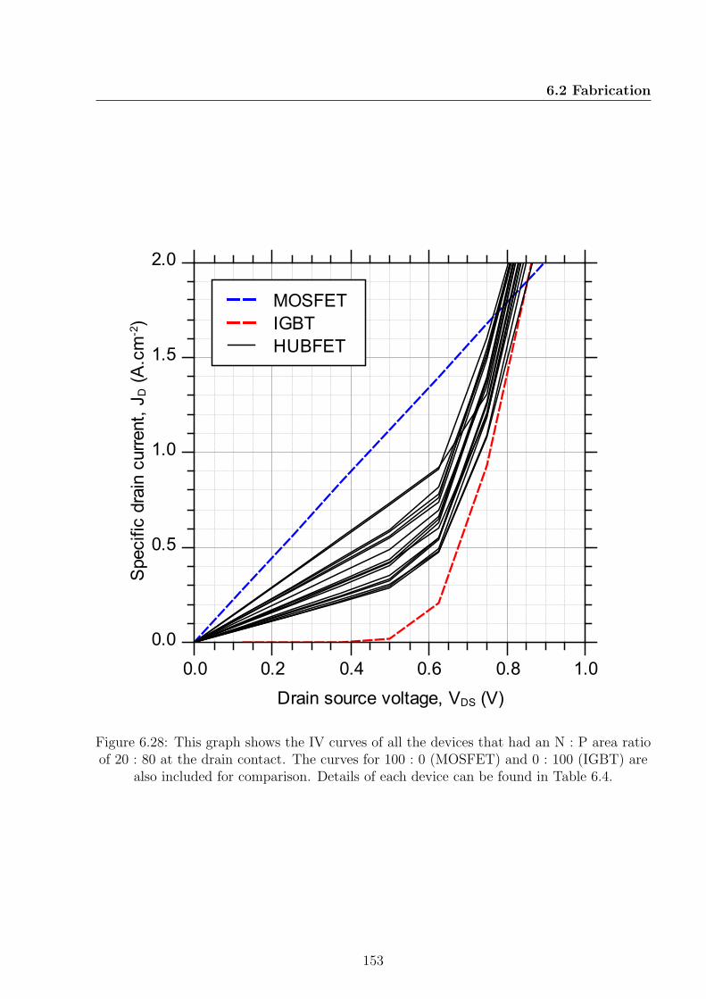
6.2 Fabrication
Specific drain current, J
D (A.cm
-2)
0.0
0.5
1.0
1.5
2.0
Drain source voltage, VDS (V)
0.0 0.2 0.4 0.6 0.8 1.0
MOSFET
IGBT
HUBFET
Figure 6.28: This graph shows the IV curves of all the devices that had an N : P area ratioof 20 : 80 at the drain contact. The curves for 100 : 0 (MOSFET) and 0 : 100 (IGBT) are
also included for comparison. Details of each device can be found in Table 6.4.
153
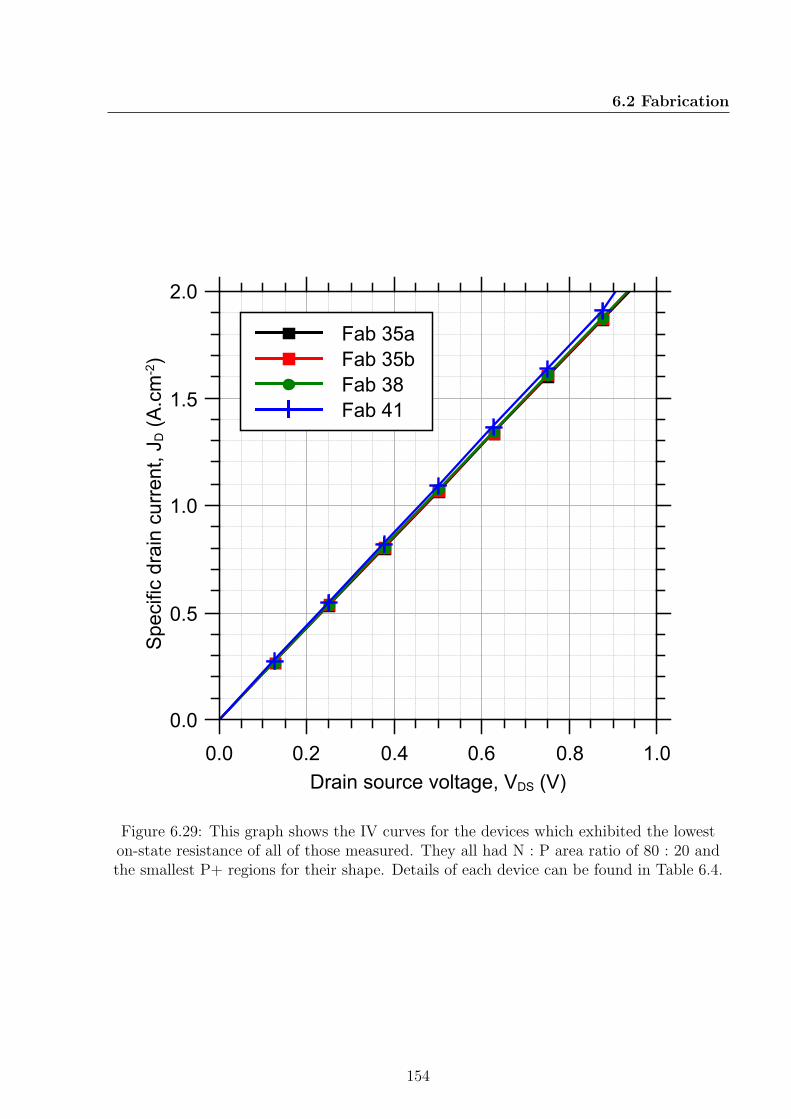
6.2 Fabrication
Specific drain current, JD (A.cm
-2)
0.0
0.5
1.0
1.5
2.0
Drain source voltage, VDS (V)
0.0 0.2 0.4 0.6 0.8 1.0
Fab 35a
Fab 35b
Fab 38
Fab 41
Figure 6.29: This graph shows the IV curves for the devices which exhibited the loweston-state resistance of all of those measured. They all had N : P area ratio of 80 : 20 andthe smallest P+ regions for their shape. Details of each device can be found in Table 6.4.
154

6.2 Fabrication
Bipolar knee voltage
• Size The size of the P+ implants appears to be the most significant factor in deter-
mining the value of Vk. Figure 6.30 shows how the minimum width of the P+ regions
(WP+(min)) impacts Vk. In this case the minimum width of the implant is defined as
the minimum distance from the centre of the smallest unit of the P+ pattern that can
be repeated to the surrounding N+ doping. This is illustrated by Figure 6.31.
• Shape The shape of the implants does not appear to influence Vk in any way other
than in relation to the minimum width as discussed above. Theoretically the circular
implants should result in a lower Vk is due to the fact the a circle with equal area
to a square will have a longer minimum width, as seen in Figure 6.32. However,
experimentally this coud not be confirmed. Despite the differing values of WP+(min)
arising from the different shapes, there was little or no difference in the bipolar knee
voltage between equivalent shapes. This can be seen in Figure 6.33. Here single areas of
P+ are made from stripes, squares and circles. Despite the differences in the geometry
of the patterns, there is little difference between the measured Vk for each part.
• Ratio Similarly to the shape, the N : P area ratio affects Vk through impacting the
minimum width of the P+ implants. The devices with N : P area ratios of 20 : 80 had
the lowest Vk because they tended to have larger P+ implant areas.
It would appear that the variations in Vk are generally due to changes in the widths of
the P+ regions that are foward biased to activate the bipolar conduction. This can be seen
in the overall trend in Figure 6.30 which shows how Vk increases as WP+(min) decreases.
155
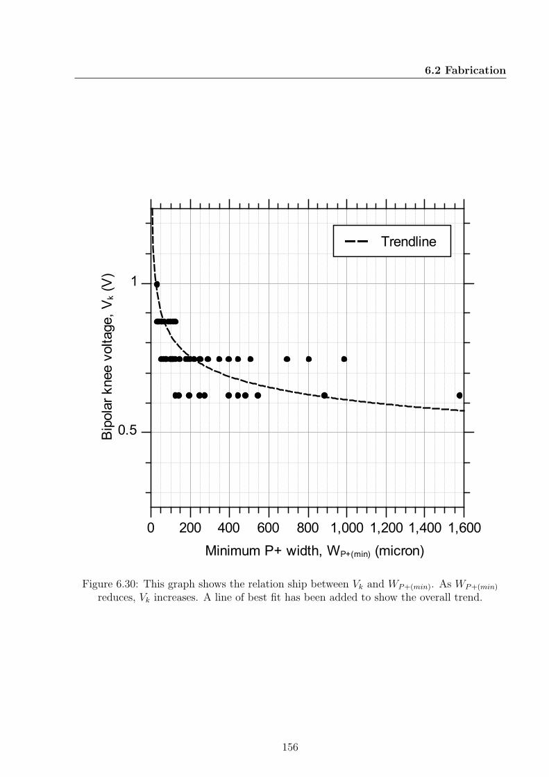
6.2 Fabrication
Bipolar knee voltage, V
k (V)
0.5
1
Minimum P+ width, WP+(min) (micron)
0 200 400 600 800 1,000 1,200 1,400 1,600
Trendline
Figure 6.30: This graph shows the relation ship between Vk and WP+(min). As WP+(min)
reduces, Vk increases. A line of best fit has been added to show the overall trend.
156
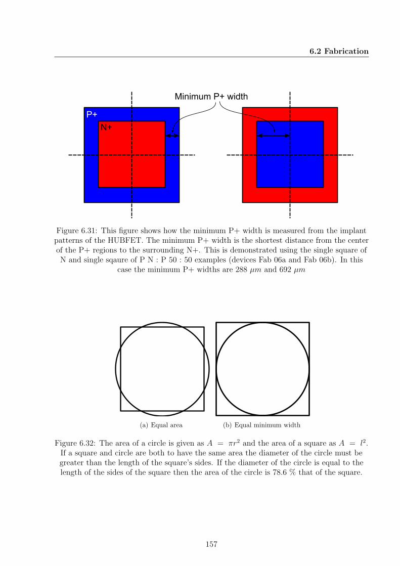
6.2 Fabrication
Minimum P+ width
P+
N+
Figure 6.31: This figure shows how the minimum P+ width is measured from the implantpatterns of the HUBFET. The minimum P+ width is the shortest distance from the centerof the P+ regions to the surrounding N+. This is demonstrated using the single square ofN and single sqaure of P N : P 50 : 50 examples (devices Fab 06a and Fab 06b). In this
case the minimum P+ widths are 288 µm and 692 µm
(a) Equal area (b) Equal minimum width
Figure 6.32: The area of a circle is given as A = πr2 and the area of a square as A = l2.If a square and circle are both to have the same area the diameter of the circle must begreater than the length of the square’s sides. If the diameter of the circle is equal to thelength of the sides of the square then the area of the circle is 78.6 % that of the square.
157
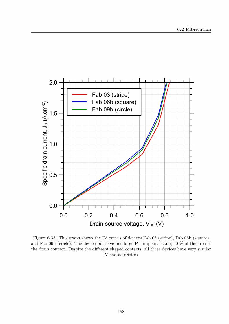
6.2 Fabrication
Specific drain current, JD (A.cm
-2)
0.0
0.5
1.0
1.5
2.0
Drain source voltage, VDS (V)
0.0 0.2 0.4 0.6 0.8 1.0
Fab 03 (stripe)
Fab 06b (square)
Fab 09b (circle)
Figure 6.33: This graph shows the IV curves of devices Fab 03 (stripe), Fab 06b (square)and Fab 09b (circle). The devices all have one large P+ implant taking 50 % of the area ofthe drain contact. Despite the different shaped contacts, all three devices have very similar
IV characteristics.
158

6.3 Analysis
6.3 Analysis
In this section the results of the simulations from Section 6.1 and measurements from Sec-
tion 6.2 are analysed. First in relation to RDS(on) and then in relation to Vk.
6.3.1 Unipolar on-state resistance
The two factors that most influenced RDS(on) are the size of the P+ implants and the ratio
of total area of N+ to P+. This can be seen in the simulated IV curves in figures 6.6,
6.7 and 6.8; the measured IV curves seen in figures 6.26, 6.27 and 6.28; and in tables 6.2
and 6.4. In conventional MOSFETs the electrons travel approximately vertically through
the drift region from the source, through the channel and on to the drain contact. As the
carriers enter the drift region at specific points (the channel) rather than being uniformly
distributed along the source contact, there is a small lateral component of their path that
marginally increases the distance travelled by the carriers. This reduces the uniformity
of the current density increasing RDS(on)sp slightly, see Figure 6.34(a). If P+ regions are
added to the drain, this lateral component is increased as the carriers cannot cross the PN
junction, they must travel around it. This longer average path effectively lengthens the drift
region for some carriers and decreases the uniformity of the current density further. As seen
in Figure 6.34(b). However, if the number of P+ regions is increased, the uniformity of
the current density also increases, as seen in Figure 6.34(c). Although the mean distance
travelled by an electron through the drift region is the same when the N+ to P+ area ratio
is constant, regardless of the number of P+ implants, the maximum distance travelled by
some of the carriers is greater for larger implants.
159
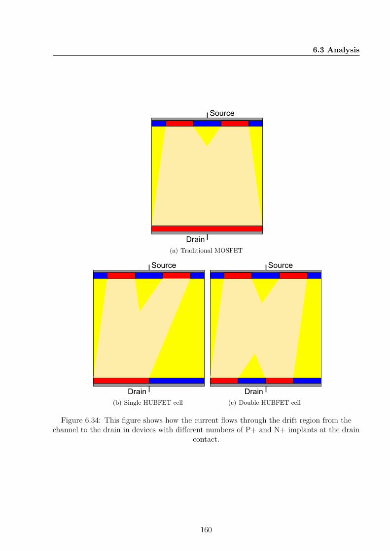
6.3 Analysis
Source
Drain
(a) Traditional MOSFET
Source
Drain
(b) Single HUBFET cell
Source
Drain
(c) Double HUBFET cell
Figure 6.34: This figure shows how the current flows through the drift region from thechannel to the drain in devices with different numbers of P+ and N+ implants at the drain
contact.
160

6.3 Analysis
This effect can be seen in Figure 6.33 where small differences in RDS(on)sp correspond
to the differences in the minimum width of the P+ implants. Here the highest value of
RDS(on)sp is seen in the striped implant where the minimum width is 1000 µm, next is the
circle, 798 µm, and finally the square, 707 µm. Therefore it is important to increase the
amount of N+ implant area relative to P+ implant area and reduce the size of the P+
implants as much as possible in order to minimise RDS(on)sp. This difference in RDS(on) was
also observed in the simulations (as seen in figures 6.6, 6.7 and 6.8.
What is less clear is what impact, if any, the shape of the P+ implants has on the on-state
resistance of the HUBFET. The results of the shape tests do not yield any clear benefits
that cannot be explained by the analysis shown above. It is possible that the shape of
the implants is more significant with regards to the switching performance and breakdown
characteristics of the HUBFET. However, this is not the subject of this study and will have
to be left for another time.
6.3.2 Bipolar knee voltage
The main parameter affecting Vk is the minimum width (WP+(min)) of the P+ regions.
WP+(min) is defined as the shortest distance a carrier would have to travel from the centre of
a P+ area to reach the surrounding N+ area. For example in a device such as Fab 06b that
consists of a single square of P doping surrounded by N doping, WP+(min) is the distance
from the centre of the P+ square to the centre of one of the edges of the square (in this
case it is 692 µm). Figure 6.30 shows the measured Vk from the physical test parts plotted
against WP+(min). As WP+(min) reduces, Vk increases and as WP+(min) approaches zero Vk
161
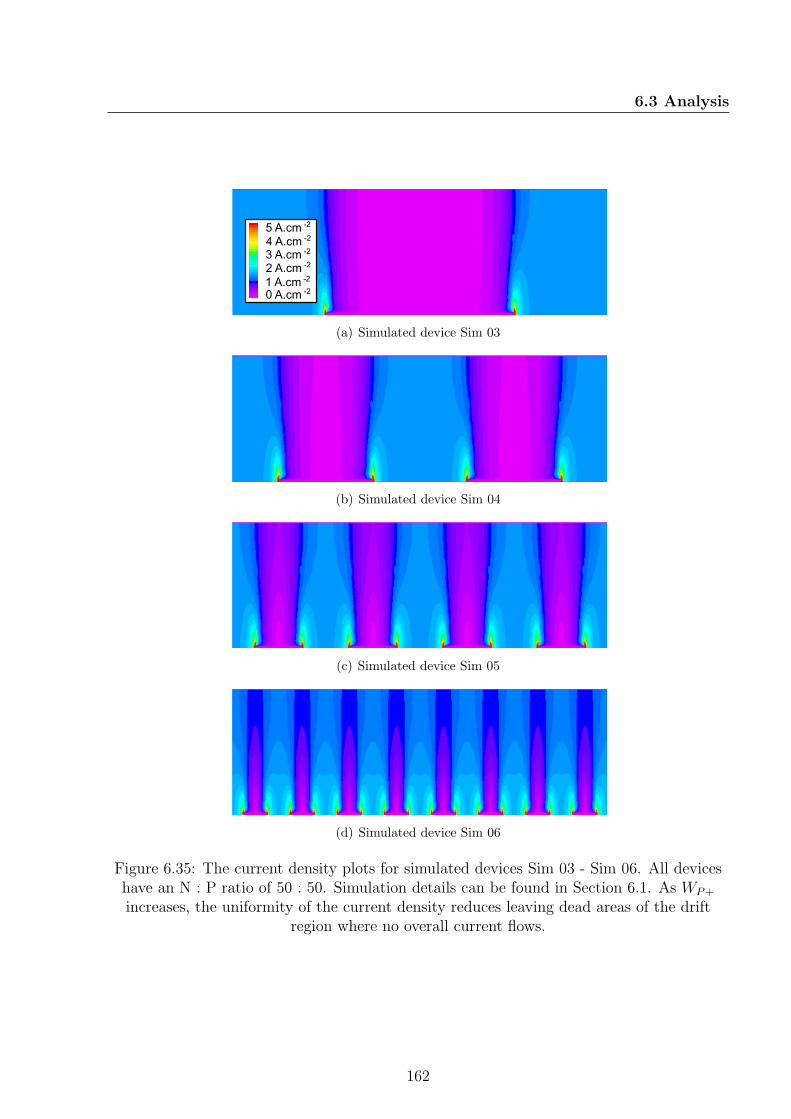
6.3 Analysis
5 A.cm -2
4 A.cm -2
3 A.cm -2
0 A.cm -2
2 A.cm -2
1 A.cm -2
(a) Simulated device Sim 03
(b) Simulated device Sim 04
(c) Simulated device Sim 05
(d) Simulated device Sim 06
Figure 6.35: The current density plots for simulated devices Sim 03 - Sim 06. All deviceshave an N : P ratio of 50 : 50. Simulation details can be found in Section 6.1. As WP+
increases, the uniformity of the current density reduces leaving dead areas of the driftregion where no overall current flows.
162

6.3 Analysis
increases rapidly. The optimum width appears to be WP+(min) > 200 µm. This result echoes
that seen in Figure 6.9 from the simulations. The cause of this is simply that the increased
distance around the P+ implant means that a greater proportion of VDS is dropped across
the implant allowing it to reach the threshold for bipolar injection at a lower VDS. This
effect was demonstrated through finite element simulation in Chapter 5. This can also be
seen in the potential plots generated from the simulations in this chapter. In Figure 6.36 it
can be seen that in devices with a higher WP+ the difference in potential between the center
of the P+ regions and the neighbouring N+ region is high, such as device Sim 03 seen in
Figure 6.36(a). However, as WP+ is reduced this difference in potential also reduces, as seen
in the potential plot from device Sim 06 in Figure 6.36(d). This will increase the value of
VDS required to forward bias the P+ region to begin bipolar conduction. The shape of the
P+ implants only appears to affect Vk because it changes the minimum dimension of the
implanted area. The best shape for the P+ implant can therefore be assumed to be a single
circle. Consider a circular implant and a square implant where the sides of the square are
equal in length to the diameter of the circle. Both of these shapes have the same minimum
distance from the centre of the shape to the edge and therefore the same Vk. However, the
circle has only 78.5 % of the area of the square. Therefore the circle is the better choice
of shape as it allows more of the drain to be implanted with N+ reducing RDS(on)sp. This
is shown in Figure 6.32. The effect of changing the area ratio is the same as changing the
shape, in that it is how the new proportions impact WP+(min) that changes Vk.
163
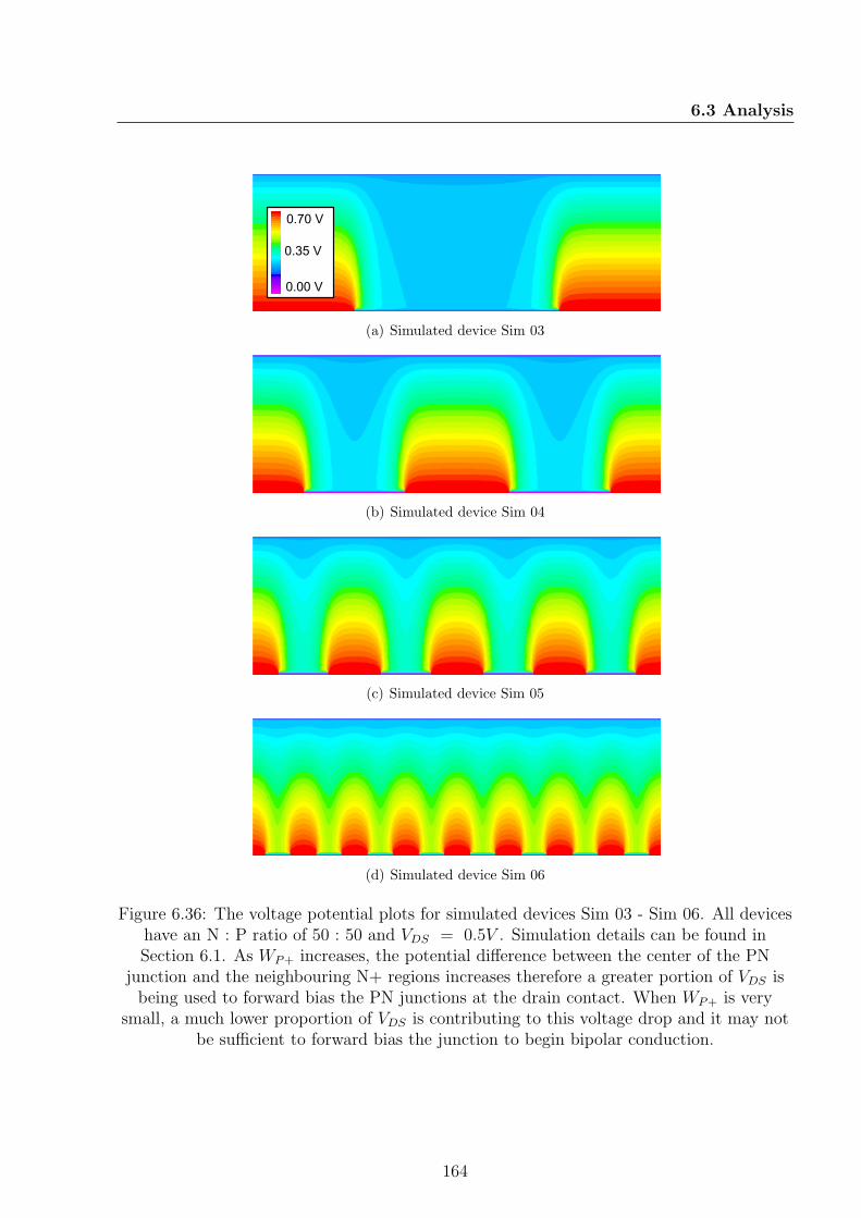
6.3 Analysis
0.70 V
0.35 V
0.00 V
(a) Simulated device Sim 03
(b) Simulated device Sim 04
(c) Simulated device Sim 05
(d) Simulated device Sim 06
Figure 6.36: The voltage potential plots for simulated devices Sim 03 - Sim 06. All deviceshave an N : P ratio of 50 : 50 and VDS = 0.5V . Simulation details can be found inSection 6.1. As WP+ increases, the potential difference between the center of the PN
junction and the neighbouring N+ regions increases therefore a greater portion of VDS isbeing used to forward bias the PN junctions at the drain contact. When WP+ is very
small, a much lower proportion of VDS is contributing to this voltage drop and it may notbe sufficient to forward bias the junction to begin bipolar conduction.
164

6.4 Summary
6.4 Summary
In this chapter it has been shown that the conclusions drawn from the simulations of Chap-
ter 5 are largely correct. However it has not been shown what the complete impact of chang-
ing the pattern of implants has on the performance of the HUBFET. Despite this, some
conclusions can be drawn the optimum pattern using the conclusions drawn from the results
of the simulations and measurements of the fabricated test parts. First, the greater the
area of N+ doping at the drain, the lower the unipolar on-state resistance of the HUBFET.
Second, the parameter that changes Vk is the minimum width of the P+ implant, as defined
in Section 6.3.2. Therefore the only shape that will not waste any N+ area because its min-
imum and maximum widths are equal is a circle. It can be assumed that in order to reduce
RDS(on) to its minimum value without impacting Vk the P+ area should take the form of a
single circular implant. It is also clear from the results of the simulations and the physical
testing that there is an optimal compromise to be found that balances a low RDS(on) with a
low Vk. This can be seen in Figure 6.37 which shows the RDS(on) plotted against Vk for all of
the simulated and fabricated structures. This can also be seen by comparing figures 6.35 and
6.36. The devices with large values of WP+, such as Sim 03 have higher RDS(on) due to the
increased distance electrons must travel through the drift region. Smaller P+ implants, such
as those seen in Sim 06 in Figure 6.35(d), have much lower RDS(on). However, in Figure 6.36
it can be seen that the proportion of VDS dropped across the P+ implants is much lower for
smaller implants, such as Sim 06 in Figure 6.36(d). This leads to an undesirable increase in
Vk. The devices with larger values of WP+, such as Sim 03 in Figure 6.36(a) have a much
greater proportion of VDS dropped across the P+ regions leading to a lower value of Vk. In
165
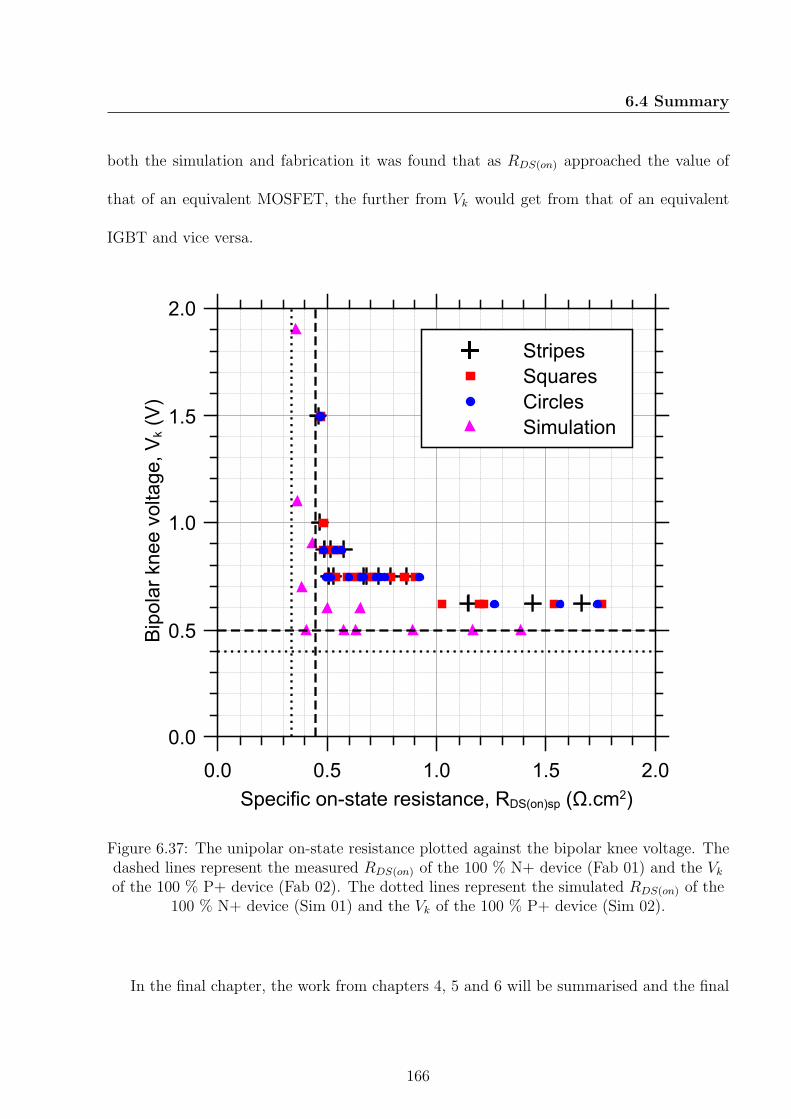
6.4 Summary
both the simulation and fabrication it was found that as RDS(on) approached the value of
that of an equivalent MOSFET, the further from Vk would get from that of an equivalent
IGBT and vice versa.
Bipolar knee voltage, Vk (V)
0.0
0.5
1.0
1.5
2.0
Specific on-state resistance, RDS(on)sp (Ω.cm2)
0.0 0.5 1.0 1.5 2.0
Stripes
Squares
Circles
Simulation
Figure 6.37: The unipolar on-state resistance plotted against the bipolar knee voltage. Thedashed lines represent the measured RDS(on) of the 100 % N+ device (Fab 01) and the Vk
of the 100 % P+ device (Fab 02). The dotted lines represent the simulated RDS(on) of the100 % N+ device (Sim 01) and the Vk of the 100 % P+ device (Sim 02).
In the final chapter, the work from chapters 4, 5 and 6 will be summarised and the final
166

6.4 Summary
conclusions will be drawn.
167

6.4 SummaryTab
le6.4:
Thistable
liststhepatternsfabricatedan
dtheirkeyparam
eters.
Pattern
Pattern
type
N:P
Are
aRatio
Bipolarkneevoltage
UnipolarR
DS(on)
Repetitions
MaxStd
.Dev.
Fab
011Squareof
N10
0:0
-0.446Ω.cm
212
0.002A
Fab
02
1SquareofP
0:100
0.500V
-12
0.003A
Fab
03
1Stripeof
N/P
50:50
0.750V
0.789Ω.cm
212
0.005A
Fab
04
1Stripeof
N/P
20:80
0.625V
1.667Ω.cm
212
0.025A
Fab
05
1Stripeof
N/P
80:20
0.750V
0.530Ω.cm
212
0.005A
Fab
06a
1SquareofN
50:50
0.750V
0.791Ω.cm
28
0.001A
Con
tinued
onnextpag
e...
168

6.4 Summary
Tab
le6.4
Continued
from
previouspage
Pattern
Pattern
type
N:P
Are
aRatio
Bipolarkneevoltage
UnipolarR
DS(on)
Repetitions
MaxStd
.Dev.
Fab
06b
1Squareof
P50:50
0.750V
0.695Ω.cm
28
0.005
A
Fab
07a
1SquareofN
20:80
0.625V
1.753Ω.cm
28
0.006
A
Fab
07b
1Squareof
P20:80
0.625V
1.190Ω.cm
28
0.013
A
Fab
08a
1SquareofN
80:20
0.750V
0.533Ω.cm
28
0.003
A
Fab
08b
1Squareof
P80:20
0.750V
0.509Ω.cm
28
0.003
A
Fab
09a
1CircleofN
50:50
0.750V
0.762Ω.cm
28
0.005
A
Fab
09b
1Circleof
P50:50
0.750V
0.722Ω.cm
28
0.012
A
Fab
101Circleof
N20:80
0.625V
1.728Ω.cm
212
0.005
A
Con
tinued
onnextpage...
169

6.4 Summary
Table
6.4
Continued
from
previouspage
Pattern
Pattern
type
N:P
Are
aRatio
Bipolarkneevoltage
UnipolarR
DS(on)
Repetitions
MaxStd
.Dev.
Fab
111Circleof
P80:20
0.750V
0.516Ω.cm
212
0.003A
Fab
122Stripes
ofN/P
50:50
0.750V
0.734Ω.cm
212
0.002A
Fab
132Stripes
ofN/P
20:80
0.625V
1.437Ω.cm
212
0.011A
Fab
142Stripes
ofN/P
80:20
0.750V
0.509Ω.cm
212
0.003A
Fab
15a
4SquaresofN
50:50
0.750V
0.715Ω.cm
28
0.004A
Fab
15b
4Squaresof
P50
:50
0.750V
0.654Ω.cm
28
0.007A
Fab
16a
4SquaresofN
20:80
0.625V
1.531Ω.cm
28
0.004A
Fab
16b
4Squaresof
P20
:80
0.625V
1.023Ω.cm
28
0.003A
Con
tinued
onnextpage...
170

6.4 Summary
Table
6.4
Continued
from
previouspage
Pattern
Pattern
type
N:P
Are
aRatio
Bipolarkneevoltage
UnipolarR
DS(on)
Repetitions
MaxStd
.Dev.
Fab
17a
4SquaresofN
80:20
0.875V
0.509Ω.cm
28
0.005A
Fab
17b
4Squaresof
P80
:20
0.750V
0.497Ω.cm
28
0.002A
Fab
18a
4Circles
ofN
50:50
0.750V
0.739Ω.cm
28
0.002A
Fab
18b
4Circles
ofP
50:50
0.750V
0.662Ω.cm
28
0.004A
Fab
194Circles
ofN
20:80
0.625V
1.562Ω.cm
212
0.005A
Fab
204Circles
ofP
80:20
0.750V
0.494Ω.cm
212
0.010A
Fab
214Stripes
ofN/P
50:50
0.750V
0.663Ω.cm
212
0.003A
Fab
224Stripes
ofN/P
20:80
0.625V
1.146Ω.cm
212
0.002A
Con
tinued
onnextpage...
171

6.4 Summary
Table
6.4
Continued
from
previouspage
Pattern
Pattern
type
N:P
Are
aRatio
Bipolarkneevoltage
UnipolarR
DS(on)
Repetitions
MaxStd
.Dev.
Fab
234Stripes
ofN/P
80:20
0.875V
0.488Ω.cm
212
0.003A
Fab
24a
16SquaresofN
50:50
0.750V
0.633Ω.cm
28
0.002A
Fab
24b
16Squares
ofP
50:50
0.750V
0.589Ω.cm
28
0.002A
Fab
25a
16SquaresofN
20:80
0.625V
1.213Ω.cm
28
0.002A
Fab
25b
16Squares
ofP
20:80
0.750V
0.849Ω.cm
28
0.002A
Fab
26a
16SquaresofN
80:20
1.000V
0.481Ω.cm
28
0.001A
Fab
26b
16Squares
ofP
80:20
0.875V
0.478Ω.cm
28
0.001A
Fab
27a
16Circles
ofN
50:50
0.750V
0.650Ω.cm
28
0.003A
Con
tinued
onnextpage...
172

6.4 Summary
Table
6.4
Continued
from
previouspage
Pattern
Pattern
type
N:P
Are
aRatio
Bipolarkneevoltage
UnipolarR
DS(on)
Repetitions
MaxStd
.Dev.
Fab
27b
16Circles
ofP
50:50
0.750V
0.598Ω.cm
28
0.003A
Fab
2816Circles
ofN
20:80
0.625V
1.257Ω.cm
212
0.006A
Fab
2916Circles
ofP
80:20
0.875V
0.479Ω.cm
212
0.001A
Fab
308Stripes
ofN/P
50:50
0.875V
0.575Ω.cm
212
0.002A
Fab
318Stripes
ofN/P
20:80
0.750V
0.862Ω.cm
212
0.002A
Fab
328Stripes
ofN/P
80:20
1.000V
0.469Ω.cm
212
0.003A
Fab
33a
64SquaresofN
50:50
0.875V
0.555Ω.cm
28
0.009A
Fab
33b
64Squares
ofP
50:50
0.875V
0.531Ω.cm
28
0.017A
Con
tinued
onnextpage...
173

6.4 Summary
Table
6.4
Continued
from
previouspage
Pattern
Pattern
type
N:P
Are
aRatio
Bipolarkneevoltage
UnipolarR
DS(on)
Repetitions
MaxStd
.Dev.
Fab
34a
64SquaresofN
20:80
0.750V
0.897Ω.cm
28
0.002A
Fab
34b
64Squares
ofP
20:80
0.750V
0.690Ω.cm
28
0.004A
Fab
35a
64Squares
ofN
80:20
>1.000V
0.469Ω.cm
28
0.003A
Fab
35b
64Squares
ofP
80:20
>1.000V
0.466Ω.cm
28
0.001A
Fab
36a
64Circles
ofN
50:50
0.875V
0.565Ω.cm
28
<0.001A
Fab
36b
64Circles
ofP
50:50
0.875V
0.535Ω.cm
28
<0.001A
Fab
37
64Circles
ofN
20:80
0.750V
0.915Ω.cm
212
0.001A
Fab
38
64Circles
ofP
80:20
>1.000V
0.465Ω.cm
212
0.001A
Con
tinued
onnextpag
e...
174
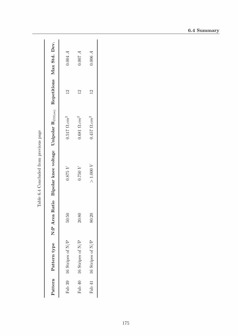
6.4 Summary
Table
6.4
Concluded
from
previouspage
Pattern
Pattern
type
N:P
Are
aRatio
Bipolarkneevoltage
UnipolarR
DS(on)
Repetitions
MaxStd
.Dev.
Fab
3916Stripes
ofN/P
50:50
0.875V
0.517Ω.cm
212
0.004
A
Fab
40
16Stripes
ofN/P
20:80
0.750V
0.681Ω.cm
212
0.007
A
Fab
41
16Stripes
ofN/P
80:20
>1.000V
0.457Ω.cm
212
0.006
A
175

Chapter
7 Conclusions
In this chapter the work completed for this thesis will be summarised and the conclusions
will be drawn. There will also be a brief discussion regarding what future work could be
carried out to build on and compliment this research. The conclusions will focus on three
key areas regarding the HUBFET. They are suitability, feasibility and improvements.
7.1 Suitability
The first question to be answered is, ‘Is the HUBFET suitable for use as a failure tolerant
switch for aircraft power systems?’. Firstly, the packaging and control of the HUBFET is
the same as a commercial MOSFET or IGBT. This means the switch can be used in any
application where MOSFETs and IGBTs are already used, which includes aircraft power
systems. However, more pressing is the question as to whether the device is electrically
suitable for the application. The answer to this question is also yes. The on-state character-
istics measured from the proof of concept devices in Chapter 5 show the device is capable
176

7.2 Feasibility
even before it is optimised. The HUBFET can be fabricated with a breakdown voltage of
1200 V and can be scaled to increase the unipolar current limit. This makes it suitable for
the majority of power switch applications in an aircraft with a reasonable but not excessive
margin of safety for use in a ± 270 V system. It exhibits the unipolar characteristic that
will allow it to perform comparably to MOSFETs under nominal conditions. It also shows
the bipolar characteristic required to handle the high surge currents typical of a short circuit
failure. The ability of the HUBFET to transistion between the unipolar and bipolar modes of
operations was demonstrated in Chapter 5. There is no reason to suggest that the HUBFET
would behave differently to the MOSFET and IGBT electrically at different temperatures.
However, the uneven current distibution at the drain contact seen in Figure 6.35, arising
from the alternating P+ and N+ regions, could lead to hot and cold spots forming. This
may have an impact on the long term reliability of the device packaging.
7.2 Feasibility
In this section the feasibility of the HUBFET as a solution to the problem of designing a
reliable power switch for use in aircraft power systems will be discussed. The work presented
in this thesis shows that the HUBFET is suitable for its task, however this is only useful if
the device can be produced on the scale required to meet the demands of the application.
The question that is to be answered is ‘Is the HUBFET a feasible and practical solution to
the need to create a failure tolerant switch for use in aircraft?’. The author would argue that
the answer to this question is a resounding yes. The main technical barrier preventing more
177

7.3 Improvements
exotic semiconductor switch designs, such as the Westmoreland hybrid and the DG-ILET
discussed in Chapter 3, from being widely adopted is modifying the commercial production
process to allow their large scale production. The most critical aspect of this is whether the
new device will require a novel packaging or control system approach. In the case of the
HUBFET the fabriction process is the same as that of the BIGT which is being designed for
commercial production. It uses the well researched and extremely widely used MOS gate for
switching control and the techniques developed for the manufacture of reverse conducting
IGBTs to fabricate its novel drain structure. Externally it has the same arrangement of
control and power terminals as a vertical power MOSFET or IGBT. This means that it does
not require a novel packaging solution, making it both easier to manufacture and easier for
consumers to use. The HUBFET’s use of a single MOS gate also eliminates the need for
any complex new control system. It is the conclusion of the author that it is both feasible
and practical to scale the HUBFET for production using available commercial processes and
operate it using existing control techniques.
7.3 Improvements
The final, and most important question, is ‘Does the HUBFET offer a real improvement
over current devices for the same application?’. Again, the answer is yes. The results from
Chapter 5 show that the HUBFET offers improvements over the power MOSFET in terms
of high current handling. This would allow a system that had previously used MOSFETs to
be designed with either the same silicon device area and a higher surge current rating or a
178

7.4 Future work
lower silicon device area for the same surge current rating. Similarly, when compared to the
IGBT, the HUBFET can offer lower power losses at lower currents for the same device area.
However, the HUBFET is not superior in every category. When compared to the IGBT, the
HUBFET would offer a reduced surge current handling capability, but this still represents
a significant improvement over the MOSFET. The results from Chapter 6 show that there
are changes that can be made to the HUBFET that will improve its performance when
compared to the initial proof of concept device seen in Chapter 5. If this can be realised
in a full HUBFET device then real significant improvements can be made to its on-state
performance.
7.4 Future work
The next step for this project would be to perform a second phase of drain pattern inves-
tigation. The results from Chapter 6 show that major improvements can be made to the
HUBFET through changes to this pattern. This could be investigated further to comfirm
the conclusions from this work. Larger area devices could be constructed with relatively
small P+ regions to determine if the bipolar action will remain strong with just a very small
area of P+ relative to N+. If it is confirmed that this is the optimum design then the next
step would be to create full gated devices in order to study the switching and long term
reliability of the switches. It is likely that this would result in further modification to the
drain implant pattern as more characteristics and the parameters that influence them are
identified. The thermal properties of the HUBFET should also be considered. The potential
179

7.4 Future work
issue of thermal hotspotting identified in Section 7.1 is one that requires further study. It is
necessary to identify how this may influence the long term reliabilty of packaged devices.
Finally, in the longer term it should be investigated how this technology can be applied
to emerging semiconductor materials such as SiC. The most obvious issue is how the SiC
wafers could be thinned in order to process the backside. SiC is an extrememly hard and
brittle material so this will present many challenges. Thinning device grade SiC wafers is
not currently possible, however a few years ago the same could have been said of Si. If the
problem of wafer thinning and handling can be overcome then a SiC HUBFET is a real
possibility. MOS gates have been fabriacted in SiC for commercial devices and SiC bipolar
devices such as PiN diodes and BJTs are emerging into the marketplace. Combining the
technologies used for these devices with the development of ultra-thin wafers, would allow a
SiC HUBFET to enter production in the future.
180
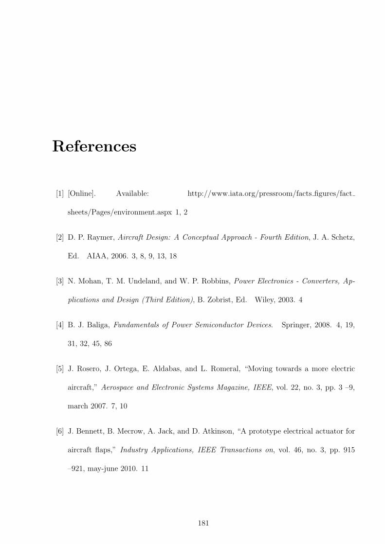
References
[1] [Online]. Available: http://www.iata.org/pressroom/facts figures/fact
sheets/Pages/environment.aspx 1, 2
[2] D. P. Raymer, Aircraft Design: A Conceptual Approach - Fourth Edition, J. A. Schetz,
Ed. AIAA, 2006. 3, 8, 9, 13, 18
[3] N. Mohan, T. M. Undeland, and W. P. Robbins, Power Electronics - Converters, Ap-
plications and Design (Third Edition), B. Zobrist, Ed. Wiley, 2003. 4
[4] B. J. Baliga, Fundamentals of Power Semiconductor Devices. Springer, 2008. 4, 19,
31, 32, 45, 86
[5] J. Rosero, J. Ortega, E. Aldabas, and L. Romeral, “Moving towards a more electric
aircraft,” Aerospace and Electronic Systems Magazine, IEEE, vol. 22, no. 3, pp. 3 –9,
march 2007. 7, 10
[6] J. Bennett, B. Mecrow, A. Jack, and D. Atkinson, “A prototype electrical actuator for
aircraft flaps,” Industry Applications, IEEE Transactions on, vol. 46, no. 3, pp. 915
–921, may-june 2010. 11
181

REFERENCES
[7] J. Weimer, “Electrical power technology for the more electric aircraft,” in Digital Avion-
ics Systems Conference, 1993. 12th DASC., AIAA/IEEE, oct 1993, pp. 445 –450. 13
[8] M. Miles, “Recent advances in lithium battery technology,” in Gallium Arsenide Inte-
grated Circuit (GaAs IC) Symposium, 2001. 23rd Annual Technical Digest, 2001, pp.
219 –222. 15, 17
[9] OMRON, “Dc power realy - g9ec-1 datasheet,” OMRON, Tech. Rep. 15
[10] S. Sze and K. K. Ng, Physics of Semiconductor Devices, 3rd ed. Wiley, 2007. 22
[11] D. Kahng, “Electric field controlled semiconductor device,” US Patent 3 102 230, 1963.
24
[12] R. F. Pierret, Semiconductor Device Fundamentals. Addison-Wesley, 1996. 29, 73, 88
[13] D. J. Coe, US Patent 4 754 310, 1988. 38
[14] X. Chen, US Patent 5,216,275, 1993. 38
[15] J. Tihanyi, US Patent 5,438,215, 1995. 38
[16] G. Deboy, N. Marz, J.-P. Stengl, H. Strack, J. Tihanyi, and H. Weber, “A new generation
of high voltage mosfets breaks the limit line of silicon,” in Electron Devices Meeting,
1998. IEDM ’98. Technical Digest., International, dec 1998, pp. 683 –685. 38, 39, 41
[17] L. Lorenz, G. Deboy, A. Knapp, and M. Marz, “Coolmostm-a new milestone in high
voltage power mos,” in Power Semiconductor Devices and ICs, 1999. ISPSD ’99. Pro-
ceedings., The 11th International Symposium on, 1999, pp. 3 –10. 38, 39
182
REFERENCES
[18] M. Saggio, D. Fagone, and S. Musumeci, “Mdmeshtm: innovative technology for high
voltage power mosfets,” in Power Semiconductor Devices and ICs, 2000. Proceedings.
The 12th International Symposium on, 2000, pp. 65 –68. 38
[19] P. Moens, F. Bogman, H. Ziad, H. De Vleeschouwer, J. Baele, M. Tack, G. Loechelt,
G. Grivna, J. Parsey, Y. Wu, T. Quddus, and P. Zdebel, “Ultimos: A local charge-
balanced trench-based 600v super-junction device,” in Power Semiconductor Devices
and ICs (ISPSD), 2011 IEEE 23rd International Symposium on, may 2011, pp. 304
–307. 40
[20] T. Tamaki, Y. Nakazawa, H. Kanai, Y. Abiko, Y. Ikegami, M. Ishikawa, E. Wakimoto,
T. Yasuda, and S. Eguchi, “Vertical charge imbalance effect on 600 v-class trench-filling
superjunction power mosfets,” in Power Semiconductor Devices and ICs (ISPSD), 2011
IEEE 23rd International Symposium on, may 2011, pp. 308 –311. 40, 41
[21] B. Jayant Baliga, “Enhancement- and depletion-mode vertical-channel m.o.s. gated
thyristors,” Electronics Letters, vol. 15, no. 20, pp. 645 –647, 27 1979. 42
[22] Yamagami, Japan Patent S47-21 739, 1972. 42
[23] B. J. Baliga, Power Semiconductor Devices, J. Plant, Ed. PWS Publishing Company,
1996. 46, 47, 74, 84
[24] H. Boving, T. Laska, A. Pugatschow, and W. Jakobi, “Ultrathin 400v fs igbt for hev
applications,” in Power Semiconductor Devices and ICs (ISPSD), 2011 IEEE 23rd In-
ternational Symposium on, may 2011, pp. 64 –67. 47, 64
183
REFERENCES
[25] Y. Haraguchi, S. Honda, K. Nakata, A. Narazaki, and Y. Terasaki, “600v lpt-cstbt
x2122; on advanced thin wafer technology,” in Power Semiconductor Devices and ICs
(ISPSD), 2011 IEEE 23rd International Symposium on, may 2011, pp. 68 –71. 47, 64
[26] S. Honda, Y. Haraguchi, A. Narazaki, T. Terashima, and Y. Terasaki, “Next generation
600v cstbt x2122; with an advanced fine pattern and a thin wafer process technologies,”
in Power Semiconductor Devices and ICs (ISPSD), 2012 24th International Symposium
on, june 2012, pp. 149 –152. 47
[27] M. Rahimo, A. Kopta, U. Schlapbach, J. Vobecky, R. Schnell, and S. Klaka, “The
bi-mode insulated gate transistor (bigt) a potential technology for higher power appli-
cations,” in Power Semiconductor Devices IC’s, 2009. ISPSD 2009. 21st International
Symposium on, june 2009, pp. 283 –286. 47, 64, 65
[28] M. Rahimo, U. Schlapbach, R. Schnell, A. Kopta, J. Vobecky, and A. Baschnagel, “Re-
alization of higher output power capability with the bi-mode insulated gate transistor
(bigt),” in Power Electronics and Applications, 2009. EPE ’09. 13th European Confer-
ence on, sept. 2009, pp. 1 –10. 47, 64, 65
[29] L. Storasta, A. Kopta, and M. Rahimo, “A comparison of charge dynamics in the
reverse-conducting rc igbt and bi-mode insulated gate transistor bigt,” in Power Semi-
conductor Devices IC’s (ISPSD), 2010 22nd International Symposium on, june 2010,
pp. 391 –394. 47, 64, 65, 90
[30] L. Storasta, M. Rahimo, M. Bellini, A. Kopta, U. Vemulapati, and N. Kaminski, “The
radial layout design concept for the bi-mode insulated gate transistor,” in Power Semi-
184

REFERENCES
conductor Devices and ICs (ISPSD), 2011 IEEE 23rd International Symposium on, may
2011, pp. 56 –59. 47, 64, 65, 93, 94, 131, 133
[31] CREE, “Cmf20120d - silicon carbide power mosfet,” Datasheet, Cree, Inc. 4600 Silicon
Drive Durham, NC 27703, Tech. Rep., 2012. 51, 54
[32] B. Baliga, “Trends in power semiconductor devices,” Electron Devices, IEEE Transac-
tions on, vol. 43, no. 10, pp. 1717 –1731, oct 1996. 51
[33] J. Palmour, R. Singh, R. Glass, O. Kordina, and J. Carter, C.H., “Silicon carbide for
power devices,” in Power Semiconductor Devices and IC’s, 1997. ISPSD ’97., 1997
IEEE International Symposium on, may 1997, pp. 25 –32. 51
[34] B. Baliga, “Trends in power discrete devices,” in Power Semiconductor Devices and
ICs, 1998. ISPSD 98. Proceedings of the 10th International Symposium on, jun 1998,
pp. 5 –10. 51
[35] R. Chilukuri, P. Shenoy, and B. Jayant Baliga, “High temperature operation of sic
planar accufet,” in Industry Applications Conference, 1998. Thirty-Third IAS Annual
Meeting. The 1998 IEEE, vol. 2, oct. 1998, pp. 954 –958 vol.2. 51
[36] A. Agarwal, S.-H. Ryu, M. Das, L. Lipkin, J. Palmour, and N. Saks, “Large area
4h-sic power mosfets,” in Power Semiconductor Devices and ICs, 2001. ISPSD ’01.
Proceedings of the 13th International Symposium on, 2001, pp. 183 –186. 51
[37] K. Matocha, “Challenges in sic power mosfet design,” in Semiconductor Device Research
Symposium, 2007 International, dec. 2007, pp. 1 –2. 51
185

REFERENCES
[38] P. Losee, K. Matocha, S. Arthur, J. Nasadoski, Z. Stum, J. Garrett, M. Schutten,
G. Dunne, and L. Stevanovic, “Dc and transient performance of 4h-sic double-implant
mosfets,” Electron Devices, IEEE Transactions on, vol. 55, no. 8, pp. 1824 –1829, aug.
2008. 51
[39] L. Stevanovic, K. Matocha, Z. Stum, P. Losee, A. Gowda, J. Glaser, and R. Beaupre,
“Realizing the full potential of silicon carbide power devices,” in Control and Modeling
for Power Electronics (COMPEL), 2010 IEEE 12th Workshop on, june 2010, pp. 1 –6.
51
[40] A. Bolotnikov, P. Losee, K. Matocha, J. Glaser, J. Nasadoski, L. Wang, A. Elasser,
S. Arthur, Z. Stum, P. Sandvik, Y. Sui, T. Johnson, J. Sabate, and L. Stevanovic, “3.3kv
sic mosfets designed for low on-resistance and fast switching,” in Power Semiconductor
Devices and ICs (ISPSD), 2012 24th International Symposium on, june 2012, pp. 389
–392. 51
[41] A. Perez-Tomas, P. Brosselard, P. Godignon, J. Millan, N. Mestres, M. R. Jennings,
J. A. Covington, and P. A. Mawby, “Field-effect mobility temperature modeling of 4h-
sic metal-oxide-semiconductor transistors,” Journal of Applied Physics, vol. 100, no. 11,
p. 114508, 2006. 51, 55
[42] A. Perez-Tomas, M. R. Jennings, P. M. Gammon, G. J. Roberts, P. A. Mawby, J. Millan,
P. Godignon, J. Montserrat, and N. Mestres, “SiC MOSFETs with thermally oxidized
Ta2Si stacked on SiO2 as high-k gate insulator,” MICROELECTRONIC ENGINEER-
ING, vol. 85, no. 4, pp. 704–709, APR 2008. 51, 55
186

REFERENCES
[43] M. R. Jennings, A. Prez-Toms, O. J. Guy, M. Lodzinski, P. Gammon, S. Burrows, J. A.
Covington, and P. A. Mawby, “Silicon-on-SiC, a Novel Semiconductor Structure for
Power Devices,” in SILICON CARBIDE AND RELATED MATERIALS 2009, PTS
1 AND 2, ser. Materials Science Forum, vol. 645-648, no. Part 1-2. TRANS TECH
PUBLICATIONS LTD, 2010, Proceedings Paper, pp. 1243–1246. 51
[44] B. Zippelius, J. Suda, and T. Kimoto, “High temperature annealing of n-type 4h-sic:
Impact on intrinsic defects and carrier lifetime,” Journal of Applied Physics, vol. 111,
no. 3, pp. 033 515 –033 515–5, feb 2012. 51
[45] M. R. Jennings, A. Prez-Toms, A. Bashir, A. Sanchez, A. Severino, P. J. Ward,
S. M. Thomas, C. Fisher, P. M. Gammon, M. Zabala, S. E. Burrows, B. Donnellan,
D. P. Hamilton, D. Walker, and P. A. Mawby, “Bow free 4 diameter 3c-sic epilayers
formed upon wafer-bonded si/sic substrates,” ECS Solid State Letters, vol. 1, no. 6,
pp. P85–P88, 2012. [Online]. Available: http://ssl.ecsdl.org/content/1/6/P85.abstract
51, 54
[46] M. R. Jennings, A. Prez-Toms, A. Severino, P. J. Ward, A. Bashir, C. Fisher, S. M.
Thomas, P. M. Gammon, B. T. Donnellan, H. Rong, D. P. Hamilton, and P. A. Mawby,
“Innovative 3c-sic on sic via direct wafer bonding,” in Proceedings of the European
Silicon Carbide and Related Materials Conference, 2012. 51
[47] B. J. Baliga, Silicon Carbide Power Devices. World Scientific Publishing Co. Pte. Ltd.,
2005, vol. 1. 52, 55, 56
187

REFERENCES
[48] M. E. Levinshtein, S. L. Rumyantsev, and M. S. Shur, Properties of Advanced Semi-
conductor Materials: GaN, AlN, InN, BN, SiC, SiGe. John Wiley & Sons, 2001.
52
[49] W. J. Choyke and L. Patrick, “Luminescence of donor-acceptor pairs in cubic
sic,” Phys. Rev. B, vol. 2, pp. 4959–4965, Dec 1970. [Online]. Available:
http://link.aps.org/doi/10.1103/PhysRevB.2.4959 52
[50] S. Dhar, S.-H. Ryu, and A. Agarwal, “A study on pre-oxidation nitrogen implantation
for the improvement of channel mobility in 4h-sic mosfets,” Electron Devices, IEEE
Transactions on, vol. 57, no. 6, pp. 1195 –1200, june 2010. 53, 55
[51] S. Dhar, S. Haney, L. Cheng, S.-R. Ryu, A. K. Agarwal, L. C. Yu, and K. P. Che-
ung, “Inversion layer carrier concentration and mobility in 4h x2013;sic metal-oxide-
semiconductor field-effect transistors,” Journal of Applied Physics, vol. 108, no. 5, pp.
054 509 –054 509–5, sep 2010. 53, 55
[52] J. Rozen, A. Ahyi, X. Zhu, J. Williams, and L. Feldman, “Scaling between channel
mobility and interface state density in sic mosfets,” Electron Devices, IEEE Transactions
on, vol. 58, no. 11, pp. 3808 –3811, nov. 2011. 53, 55
[53] IXYS, “Ixfk 30n100q2 hiperfet,” Tech. Rep., 2004. 54
[54] O. Alatise, N.-A. Parker-Allotey, D. Hamilton, and P. Mawby, “The impact of parasitic
inductance on the performance of silicon x2013;carbide schottky barrier diodes,” Power
Electronics, IEEE Transactions on, vol. 27, no. 8, pp. 3826 –3833, aug. 2012. 54
188

REFERENCES
[55] Z. Chen, D. Boroyevich, R. Burgos, and F. Wang, “Characterization and modeling of
1.2 kv, 20 a sic mosfets,” in Energy Conversion Congress and Exposition, 2009. ECCE
2009. IEEE, sept. 2009, pp. 1480 –1487. 54
[56] F. Udrea, G. Amaratunga, J. Humphrey, J. Clark, and A. Evans, “Inversion layer
injection devices - a new class of semiconductor devices,” in Solid State Device Research
Conference, 1996. ESSDERC ’96. Proceedings of the 26th European, sept. 1996, pp. 241
–244. 58, 61
[57] F. Udrea, U. Udugampola, K. Sheng, R. McMahon, G. Amaratunga, E. Narayanan,
M. De Souza, and S. Hardikar, “Experimental demonstration of an ultra-fast double
gate inversion layer emitter transistor (dg-ilet),” Electron Device Letters, IEEE, vol. 23,
no. 12, pp. 725 –727, dec. 2002. 58
[58] M. Westmoreland, P. Ward, and P. Mawby, “Introduction of a hybrid mosfet-igbt power
switching device utilising a novel schottky biased minority carrier injector,” in Power
Electronics and Applications (EPE 2011), Proceedings of the 2011-14th European Con-
ference on, 30 2011-sept. 1 2011, pp. 1 –10. 59, 62, 63
[59] A. Bourennane, J. Sanchez, F. Richardeau, and M. Imbernon, E. andBreil, “On the
integration of a pin diode and an igbt for a specific application,” in Proceedings of the
International Seminar on Power Semiconductors, 2006, p. 145. 69
[60] M. S. Shur, Physics of Semiconductor Devices. Prentice-Hall, 1990. 86
189

REFERENCES
[61] B. Donnellan, A. T. Bryant, and P. A. Mawby, “Modelling of current sharing in par-
allelel current limiting superjunction mosfets with common gate drive,” in ISPS 10
Proceedings, September 2010. 87
[62] B. Donnellan, G. Roberts, P. Mawby, and A. Bryant, “Modelling of current sharing
in paralleled current limiting superjunction mosfets with common gate drives,”
Microelectronics Reliability, vol. 52, no. 3, pp. 497 – 502, 2012. [Online]. Available:
http://www.sciencedirect.com/science/article/pii/S002627141100521X 87
[63] F. J. Morin and J. P. Maita, “Electrical properties of silicon containing arsenic
and boron,” Phys. Rev., vol. 96, pp. 28–35, Oct 1954. [Online]. Available:
http://link.aps.org/doi/10.1103/PhysRev.96.28 88
[64] H. J. McSkimin, “Measurement of elastic constants at low temperatures by means of
ultrasonic waves–data for silicon and germanium single crystals, and for fused silica,”
Journal of Applied Physics, vol. 24, no. 8, pp. 988–997, 1953. [Online]. Available:
http://link.aip.org/link/?JAP/24/988/1 88
[65] P. Norton, T. Braggins, and H. Levinstein, “Impurity and lattice scattering
parameters as determined from hall and mobility analysis in n-type sili-
con,” Phys. Rev. B, vol. 8, pp. 5632–5653, Dec 1973. [Online]. Available:
http://link.aps.org/doi/10.1103/PhysRevB.8.5632 88
[66] C. Canali, G. Majni, R. Minder, and G. Ottaviani, “Electron and hole drift velocity
measurements in silicon and their empirical relation to electric field and temperature,”
Electron Devices, IEEE Transactions on, vol. 22, no. 11, pp. 1045 – 1047, nov 1975. 88
190

REFERENCES
[67] B. Donnellan, P. Mawby, M. Rahimo, and L. Storasta, “Introducing a 1200v vertical
merged igbt and power mosfet: The hubfet,” in Applied Power Electronics Conference
and Exposition (APEC), 2012 Twenty-Seventh Annual IEEE, feb. 2012, pp. 152 –156.
91, 92, 116
[68] IXYS, “Ixfk 20n120 technical datasheet,” IXYS, Tech. Rep., 2003. 95
[69] I. Rectifier, “Irgp30b120kd-ep technical datasheet,” IR, Tech. Rep., 2004. 95
[70] Shipley, “Microposit s1800 series photo resists datasheet,” Shipley, Tech. Rep. 211
[71] Rohm and Haas, “Megaposit spr220 series photresists datasheet,” Electronic Materials,
Tech. Rep., 2004. 214
191

Appendix
A Mask designs
In this appendix the different patterns used to fabricate the test parts from Chapter 6 are
shown as well as the complete wafer layout.
A.1 Masks
192
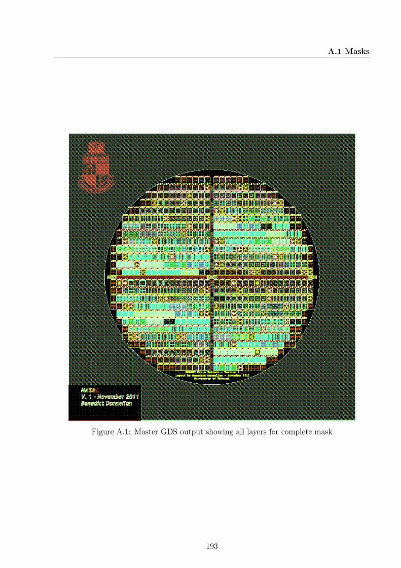
A.1 Masks
Figure A.1: Master GDS output showing all layers for complete mask
193
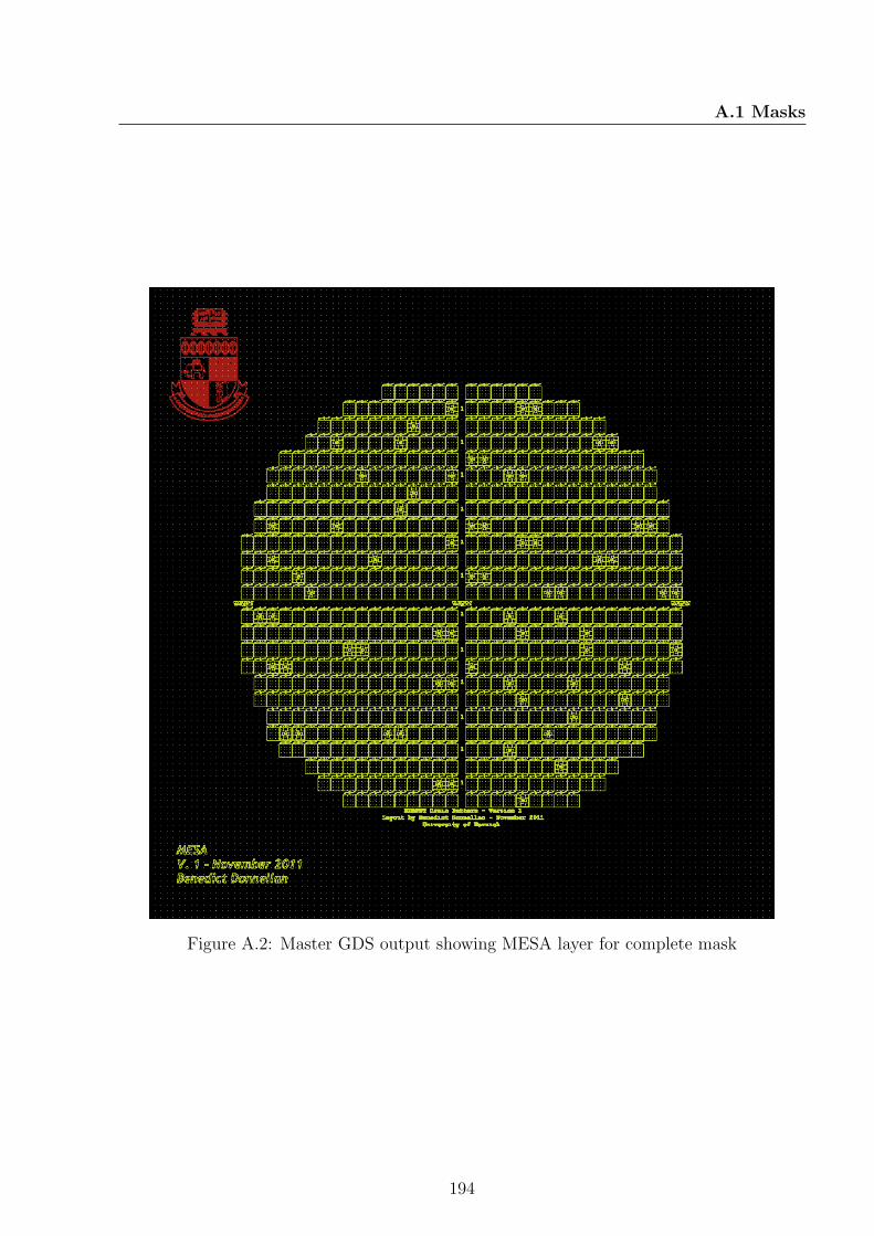
A.1 Masks
Figure A.2: Master GDS output showing MESA layer for complete mask
194

A.1 Masks
Figure A.3: Master GDS output showing N+ layer for complete mask
195
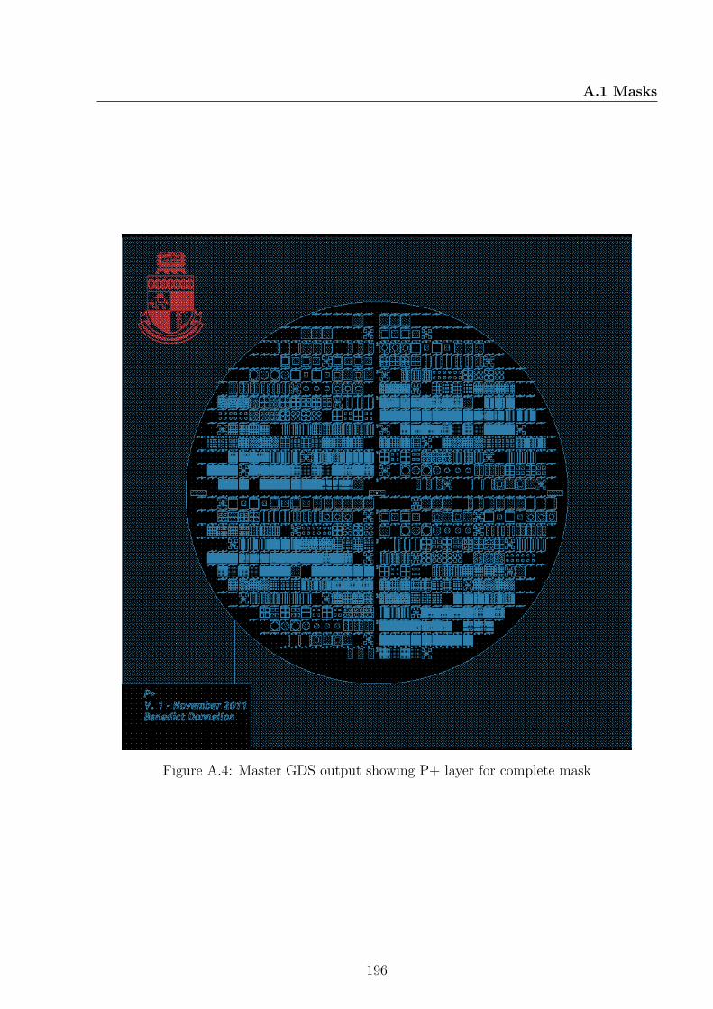
A.1 Masks
Figure A.4: Master GDS output showing P+ layer for complete mask
196
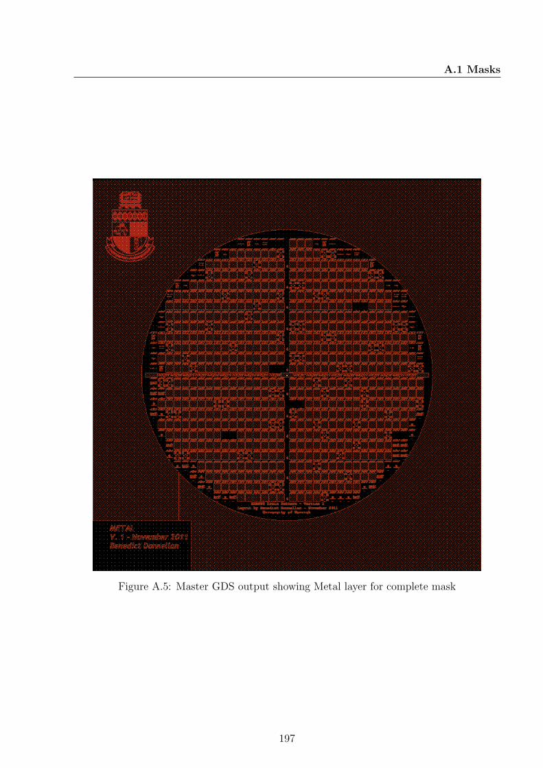
A.1 Masks
Figure A.5: Master GDS output showing Metal layer for complete mask
197
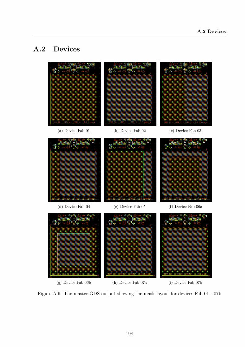
A.2 Devices
A.2 Devices
(a) Device Fab 01 (b) Device Fab 02 (c) Device Fab 03
(d) Device Fab 04 (e) Device Fab 05 (f) Device Fab 06a
(g) Device Fab 06b (h) Device Fab 07a (i) Device Fab 07b
Figure A.6: The master GDS output showing the mask layout for devices Fab 01 - 07b
198
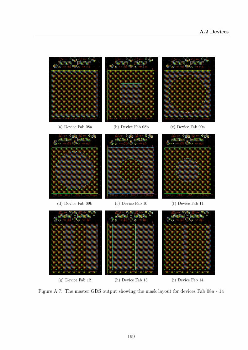
A.2 Devices
(a) Device Fab 08a (b) Device Fab 08b (c) Device Fab 09a
(d) Device Fab 09b (e) Device Fab 10 (f) Device Fab 11
(g) Device Fab 12 (h) Device Fab 13 (i) Device Fab 14
Figure A.7: The master GDS output showing the mask layout for devices Fab 08a - 14
199

A.2 Devices
(a) Device Fab 15a (b) Device Fab 15b (c) Device Fab 16a
(d) Device Fab 16b (e) Device Fab 17a (f) Device Fab 17b
(g) Device Fab 18a (h) Device Fab 18b (i) Device Fab 19
Figure A.8: The master GDS output showing the mask layout for devices Fab 15a - 19
200
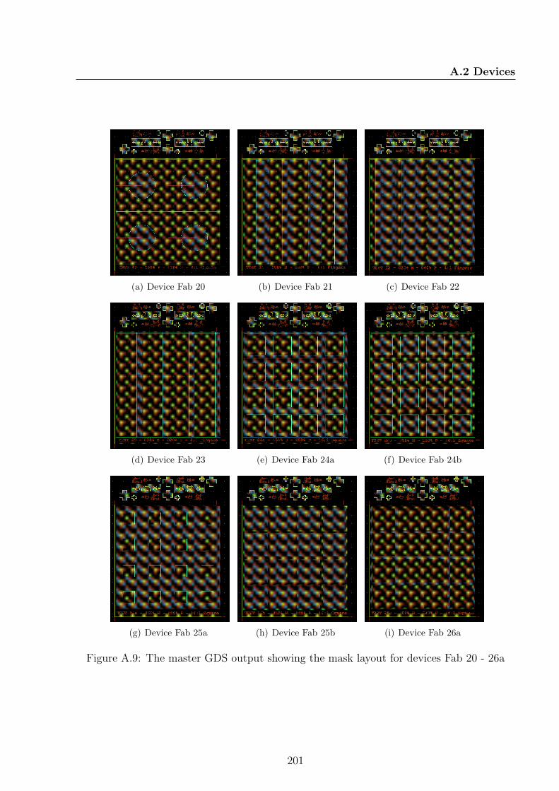
A.2 Devices
(a) Device Fab 20 (b) Device Fab 21 (c) Device Fab 22
(d) Device Fab 23 (e) Device Fab 24a (f) Device Fab 24b
(g) Device Fab 25a (h) Device Fab 25b (i) Device Fab 26a
Figure A.9: The master GDS output showing the mask layout for devices Fab 20 - 26a
201
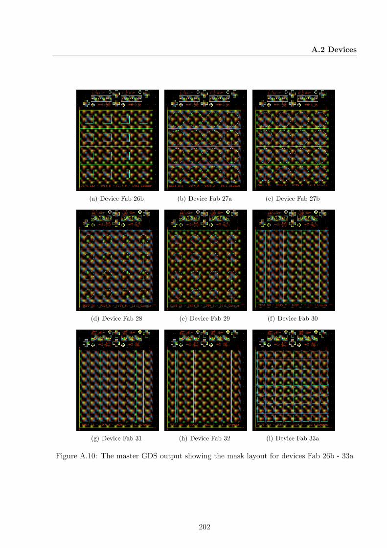
A.2 Devices
(a) Device Fab 26b (b) Device Fab 27a (c) Device Fab 27b
(d) Device Fab 28 (e) Device Fab 29 (f) Device Fab 30
(g) Device Fab 31 (h) Device Fab 32 (i) Device Fab 33a
Figure A.10: The master GDS output showing the mask layout for devices Fab 26b - 33a
202
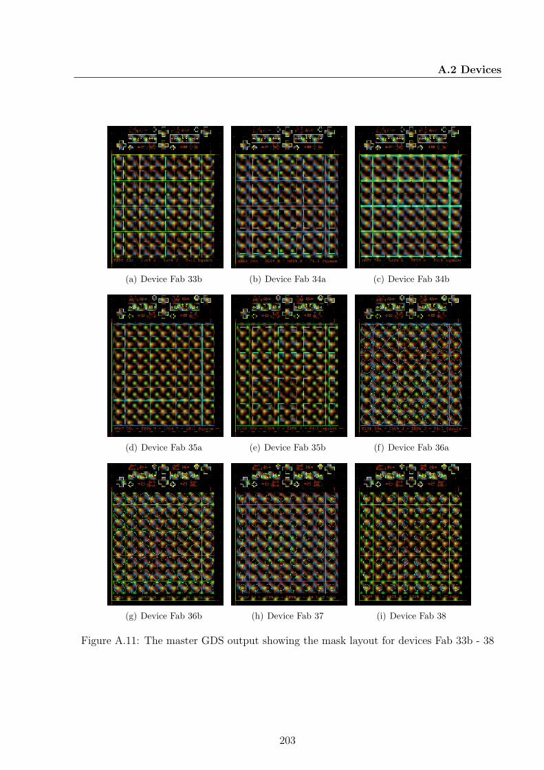
A.2 Devices
(a) Device Fab 33b (b) Device Fab 34a (c) Device Fab 34b
(d) Device Fab 35a (e) Device Fab 35b (f) Device Fab 36a
(g) Device Fab 36b (h) Device Fab 37 (i) Device Fab 38
Figure A.11: The master GDS output showing the mask layout for devices Fab 33b - 38
203
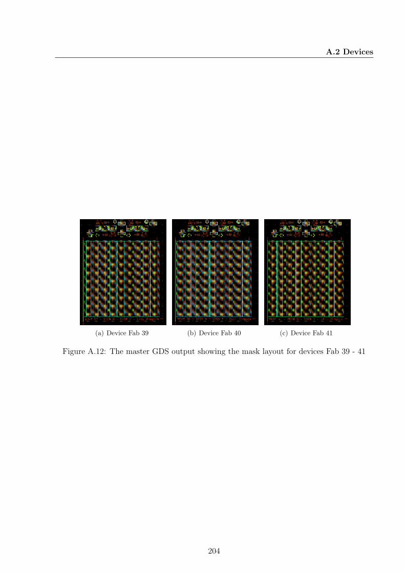
A.2 Devices
(a) Device Fab 39 (b) Device Fab 40 (c) Device Fab 41
Figure A.12: The master GDS output showing the mask layout for devices Fab 39 - 41
204

Appendix
B Fabrication process flow
This appedix describes in detail the process flow used to fabricate the test devices described
in Chapter 6
B.1 Generic processes
B.1.1 RCA clean
The RCA clean was used to prepare the wafers for processing after they had been returned
from the reduction stage.
Equipment
• Dedicated extracted wet bench
• Acid proof apron, gloves and sleeves
• Clear safety glasses
205

B.1 Generic processes
• Face shield
• Wafer carrier basket
• De-ionised (DI) water rinse tank
• Hotplate at 80oC
• Tweezers
• Timer
• 2 × quartz container (5 in) 1500 ml
• Measuring beaker 1000 ml
• Measuring beaker 100 ml
• Rinse Beaker 2000 ml
• N2 gun
Materials
• Ammonium Hydroxide (NH4OH) 25% conc.
• Hydrochloric Acid (HCL) 36% conc.
• Hydrogen Peroxide (H2O2)
• DI water (DI)
206

B.1 Generic processes
Process
Protective equipment must be worn at all times whilst performing this procedure. All
equipment must be rinsed thoroughly before and after use with DI water.
1. Prepare SC1 and SC2 acid mixes in quartz flasks.
(a) SC1 mix - NH4OH : H2O2 : DI - 1 : 1 : 5
(b) SC2 mix - HCL : H2O2 : DI - 1 : 1 : 5
2. Set hotplate to 80 oC and place SC1 mix on for 10 min to allow it to reach temperature
3. Fill rinse beaker with DI water
4. Place wafer into wafer carrier basket and place in SC1 for 10 min
5. Remove wafer from SC1 and place into rinse beaker for 1 min then into DI weir for
3 min
6. Remove SC1 from hot plate, allow to cool, aspirate away acid and thoroughly rinse
quartz container
7. Place SC2 mix onto hotplate for 15 min to allow it to reach temperature
8. Refill DI rinse beaker
9. Transfer wafer to SC2 for 10 min
10. Remove wafer from SC1 and place into rinse beaker for 1 min then into DI weir for
5 min
207

B.1 Generic processes
11. Remove SC2 from hot plate, allow to cool, aspirate away acid and thoroughly rinse
quartz container
12. Dry wafer with N2 gun and thoroughly rinse all equipment
B.1.2 S1813/1818 photoresist
This procedure is used to pattern wafers with S1813 or S1818 photoresist. This process was
used to create the pattern for the mesa etch.
Equipment
• Large dish (large enough to contain sample)
• Hotplate at 120 oC
• Hotplate at 80 oC
• Spinner
• MJB3 mask aligner
• N2 gun
• Pipette
• Tweezers
• Inspection microscope
• Profileometer
208

B.1 Generic processes
Materials
• S1813 or S1818 photoresist
• MF319 Developer
• Primer
• Acetone (MOS grade)
• Isopropanol
• DI water
Process
1. Dehydrate the sample for 1 min on 120 oC hotplate. Remove and hold in tweezers for
1 min to prevent thermal shock. Cover wafer surface with primer using pipette, leave
for 1 min then dry with N2.
2. Place sample on spinner and apply photoresist with a pipette. Use thickness curves
shown in Figure B.1 to determine speed and spin for 7 s.
3. Transfer wafer to 120 oC hotplate. Bake for 3 min. Hold in tweezers for 1min to allow
to cool before proceeding. This prevents thermal shock from cracking the photoresist.
4. Expose for 18 s using MJB3 mask aligner.
5. Fill large dish with MF319 developer. Submerge sample and develop for 40 s, agitating
gently to ensure photoresist is removed. Remove sample from developer, rinse with DI
209

B.1 Generic processes
water and dry with N2 gun.
6. Inspect with microscope to ensure good feature definition. If under or over developed
use acetone and isopropanol to clean off photoresist and restart process adjusting
exposure and developing times accordingly.
7. If feature definition is satisfactory, check photoresist step height with profileometer. If
step height is too high or too low use acetone and isopropanol to clean off photoresist
and restart process adjusting spin speed accordingly.
8. If the pattern passes all inspections, hard bake photoresist at 80 oC for 120 min to
remove all remaining solvent.
B.1.3 SPR220-7 photoresist
This procedure is used to pattern wafers with SPR220-7 photoresist. This process was used
to provide the patterns for the implantation stages.
Equipment
• Beaker (50 ml)
• Beaker (Large enough for sample)
• Hotplate at 115 oC
• Hotplate at 80 oC
• Spinner
210
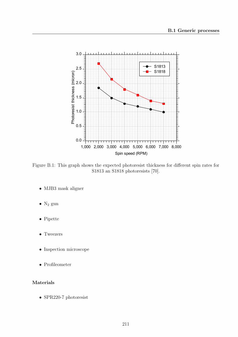
B.1 Generic processes
Photoresist thickness (micron)
0.0
0.5
1.0
1.5
2.0
2.5
3.0
Spin speed (RPM)
1,000 2,000 3,000 4,000 5,000 6,000 7,000 8,000
S1813
S1818
Figure B.1: This graph shows the expected photoresist thickness for different spin rates forS1813 an S1818 photoresists [70].
• MJB3 mask aligner
• N2 gun
• Pipette
• Tweezers
• Inspection microscope
• Profileometer
Materials
• SPR220-7 photoresist
211

B.1 Generic processes
• MF-26A developer
• Primer
• Acetone
• Isopropanol
• DI water
Process
1. Dehydrate the sample for 1 min on 115 oC hotplate. Remove and hold in tweezers for
1 min to prevent thermal shock. Cover wafer surface with primer using pipette, leave
for 1 min then dry with N2.
2. Transfer small quantity (approx 10 ml for 3 in wafer) of SPR220-7 into small beaker.
Clean neck of photoresist bottle with acetone to prevent residual liquid drying and
contaminating the rest of the bottle. Place sample on spinner and pour on SPR220-7
from the beaker. Use thickness curves shown in Figure B.2 to determine speed and
spin for 35 s. Leave after finishing for 1 min to allow photoresist to settle.
3. Transfer wafer to 115 oC hotplate. Bake for 5 min. Hold in tweezers for 1 min to
allow to cool before proceeding. This prevents thermal shock from cracking the resist.
4. Expose for 18 s using MJB3 mask aligner. Thicker photoresists require a higher buld
intensity for full exposure.
212

B.1 Generic processes
5. Store wafer away from light sources for 30 − 60 min. This time is required as the
photo active compound takes time to breakdown in the thick resist.
6. Transfer a generous amount (150 ml when using a 3 in wafer) of MF-26A developer to
the large beaker. Submerge sample and develop for 5 min, agitate gently every minute
to ensure resist is removed. Remove sample from developer, rinse with DI water and
dry with N2 gun.
7. Inspect with microscope to ensure good feature definition. If under or over developed
use acetone and isopropanol to clean off photoresist and restart process adjusting
exposure and developing times accordingly.
8. If feature definition is satisfactory, check photoresist step height with profileometer. If
step height is too high or too low use acetone and isopropanol to clean off photoresist
and restart process adjusting spin speed accordingly.
9. If the pattern passes all inspections, hard bake photoresist at 80 oC for a minimum of
120 min to remove all remaining solvent.
213

B.2 Fabrication process flow
Photo
resis
t th
ickness (m
icro
n)
0
1
2
3
4
5
6
7
8
9
10
Spin speed (RPM)
1,000 2,000 3,000 4,000 5,000 6,000 7,000 8,000
SPR220-7
Figure B.2: This graph shows the expected photoresist thickness for different spin rates forSPR220-7 photoresist [71].
B.2 Fabrication process flow
In this section the fabrication process flow used to produce the test devices used in Chapter 6
is described in detail. Figures B.3, B.4, B.5, B.6 and B.7 show a pictoral representation of
the full fabrication process.
B.2.1 Wafer preparation
The wafers purchased for this project were 100 mm epi wafers from CEMAT, Poland. In
order to be processed in the Science City Cleanroom Facility at the University of Warwick
it was necessary to reduce the diameter of the wafers to 75 mm. This process was per-
214

B.2 Fabrication process flow
formed by Loadpoint, Swindon. Upon return the wafers were RCA cleaned as described in
Section B.1.1.
B.2.2 MESA etch
The first step of the fabrication process is the MESA etch. The MESA etch defines the
alignment marks and isolates the areas where the devices will be fabricated. Each device
is approx 2 × 2 mm with alignment accuracy of approximately 1um. The process flow is
shown in Figure B.3.
1. Begin with an RCA cleaned silicon wafer.
2. Coat the wafers with S1818 photoresist using the process described in Section B.1.2 to
a thickness of 2µm.
3. Expose using the MJB3 mask aligner using the MESA mask and develop.
4. Perform a 10 min vertical silicon dry etch using an ICP etcher.
5. Remove photoresist with acetone and rinse with isopropanol.
B.2.3 N+ implantation
Following the mesa etch the N+ implant stage was performed as shown in Figure B.4.
6. Deposit SPR220-7 photoresist to a thickness of 4.5 µm using the process described in
Section B.1.3.
215

B.2 Fabrication process flow
Table B.1: This table lists the values of the parameters for the implants used in thefabrication of the HUBFET drain pattern test parts
Parameter N+ Implant P+ Implant
Species Phosphorus Boron
Dose 5× 1015 cm−2 5× 1015 cm−2
Energy 150 keV 60 keV
Tilt 7o 7o
7. Expose using the MJB3 mask aligner using the ‘N+’mask and develop in MF-26A.
8. The implantation itself was carried out at Cutting Edge Ions LLC in California, USA.
The implantation parameters can be found in Table B.1.
9. The photoresist was removed using the ash program in the ICP etcher.
B.2.4 P+ implantation
Following the N+ implantation the P+ implant stage and implant anneal were performed
as shown in Figure B.5.
10. Deposit SPR220-7 photoresist to a thickness of 4.5 µm using the process described in
Section B.1.3.
11. Expose using the MJB3 mask aligner using the ‘P+’mask and develop in MF-26A.
12. The implantation itself was carried out at Cutting Edge Ions LLC in California, USA.
The implantation parameters can be found in Table B.1.
13. The photoresist was removed using the ash program in the ICP etcher.
216

B.2 Fabrication process flow
14. After the N+ and P+ implantations had been carried out, the wafer was annealed to
activate and drive in the implant impurities. This was carried out in a pure argon
environment at 1100 oC for 30 min. After this process the implants stretched to a
depth of approximately 2 µm.
B.2.5 Metalisation
The metalisation of the test parts was achieved through a bi-layer lift-off process using SF6
and S1813 photoresists.
15. Coat the wafer in primer and leave for 1 min. Dry with N2. Spin SF6 at 4000 RPM
for 8 s and bake for 5 min at 180 oC.
16. Blanket expose the SF6 in a UV light box for 1 min
17. Apply the S1813 photoresist over the SF6 using the process described in Section B.1.2.
18. Expose the S1813 with the MJB3 mask aligner using the ‘Metal’mask. Develop using
MF319 developer. Use the inspection microscope to ensure there is a strong undercut
below the S1813.
19. Deposit 250 nm of Aluminium using a 10 min 250 W aluminium sputter. Ensure the
wafer is kept cool to prevent oxidisation.
20. Lift-off the aluminium with an ultrasonic acetone bath and remove the remaining SF6
with remover.
217

B.2 Fabrication process flow
21. Deposit 250 nm of Aluminium using a 10min 250W aluminium sputter to the backside
of the wafer. Ensure the wafer is kept cool to prevent oxidisation.
22. Anneal the contacts in the sputterer in a pure argon environment at 425 oC for 10 min.
218
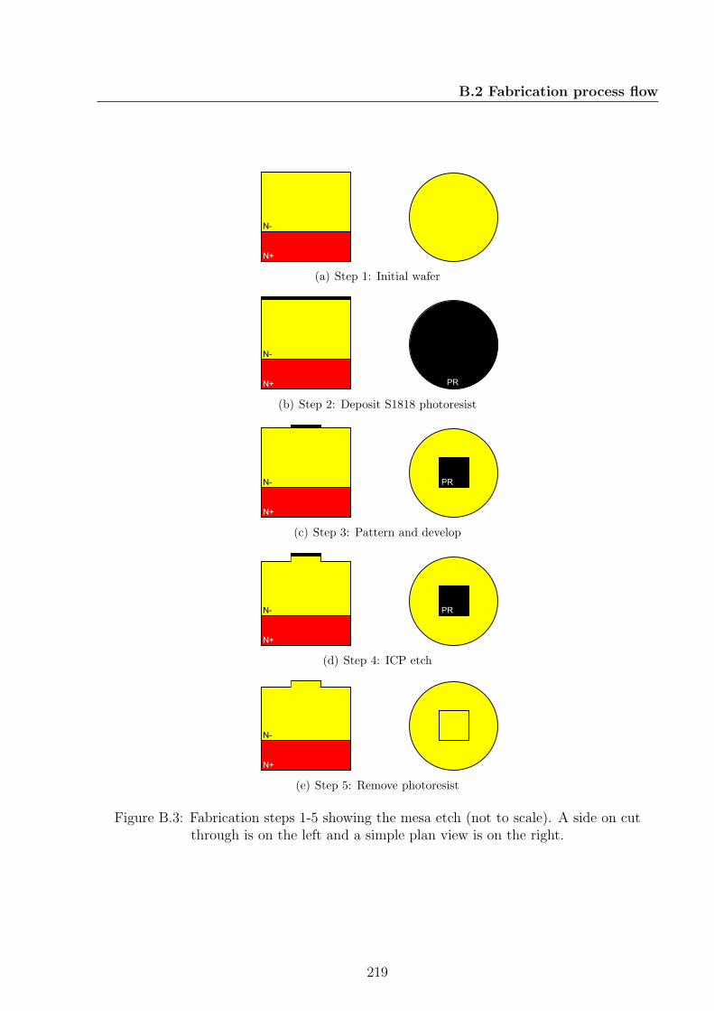
B.2 Fabrication process flow
N+
N-
(a) Step 1: Initial wafer
N+
N-
PR
(b) Step 2: Deposit S1818 photoresist
N+
N- PR
(c) Step 3: Pattern and develop
N+
N- PR
(d) Step 4: ICP etch
N+
N-
(e) Step 5: Remove photoresist
Figure B.3: Fabrication steps 1-5 showing the mesa etch (not to scale). A side on cutthrough is on the left and a simple plan view is on the right.
219
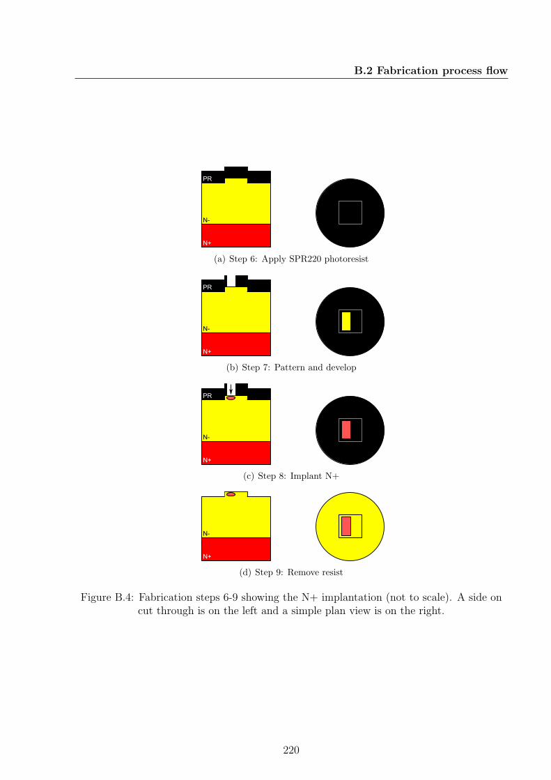
B.2 Fabrication process flow
N+
N-
PR
(a) Step 6: Apply SPR220 photoresist
N+
N-
PR
(b) Step 7: Pattern and develop
N+
N-
PR
(c) Step 8: Implant N+
N+
N-
(d) Step 9: Remove resist
Figure B.4: Fabrication steps 6-9 showing the N+ implantation (not to scale). A side oncut through is on the left and a simple plan view is on the right.
220
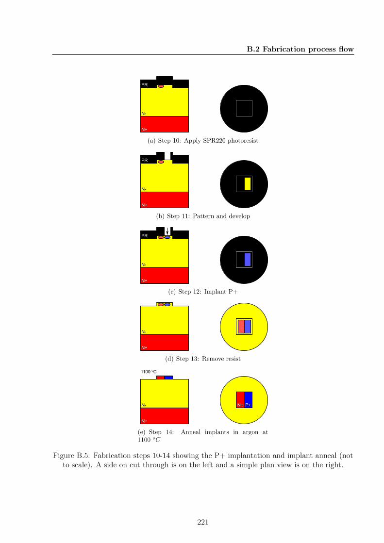
B.2 Fabrication process flow
N+
N-
PR
(a) Step 10: Apply SPR220 photoresist
N+
N-
PR
(b) Step 11: Pattern and develop
N+
N-
PR
(c) Step 12: Implant P+
N+
N-
(d) Step 13: Remove resist
N+
N- N+ P+
1100 oC
(e) Step 14: Anneal implants in argon at1100 oC
Figure B.5: Fabrication steps 10-14 showing the P+ implantation and implant anneal (notto scale). A side on cut through is on the left and a simple plan view is on the right.
221
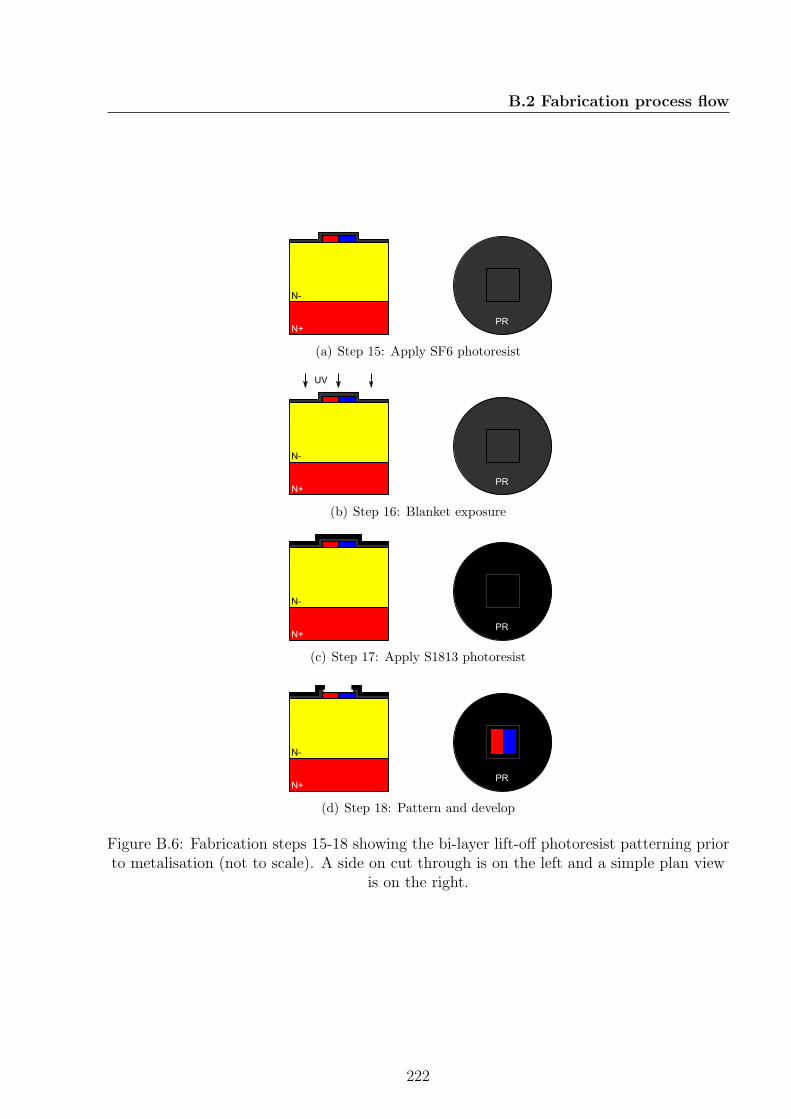
B.2 Fabrication process flow
N+
N-
PR
(a) Step 15: Apply SF6 photoresist
N+
N-
PR
UV
(b) Step 16: Blanket exposure
N+
N-
PR
(c) Step 17: Apply S1813 photoresist
N+
N-
PR
(d) Step 18: Pattern and develop
Figure B.6: Fabrication steps 15-18 showing the bi-layer lift-off photoresist patterning priorto metalisation (not to scale). A side on cut through is on the left and a simple plan view
is on the right.
222
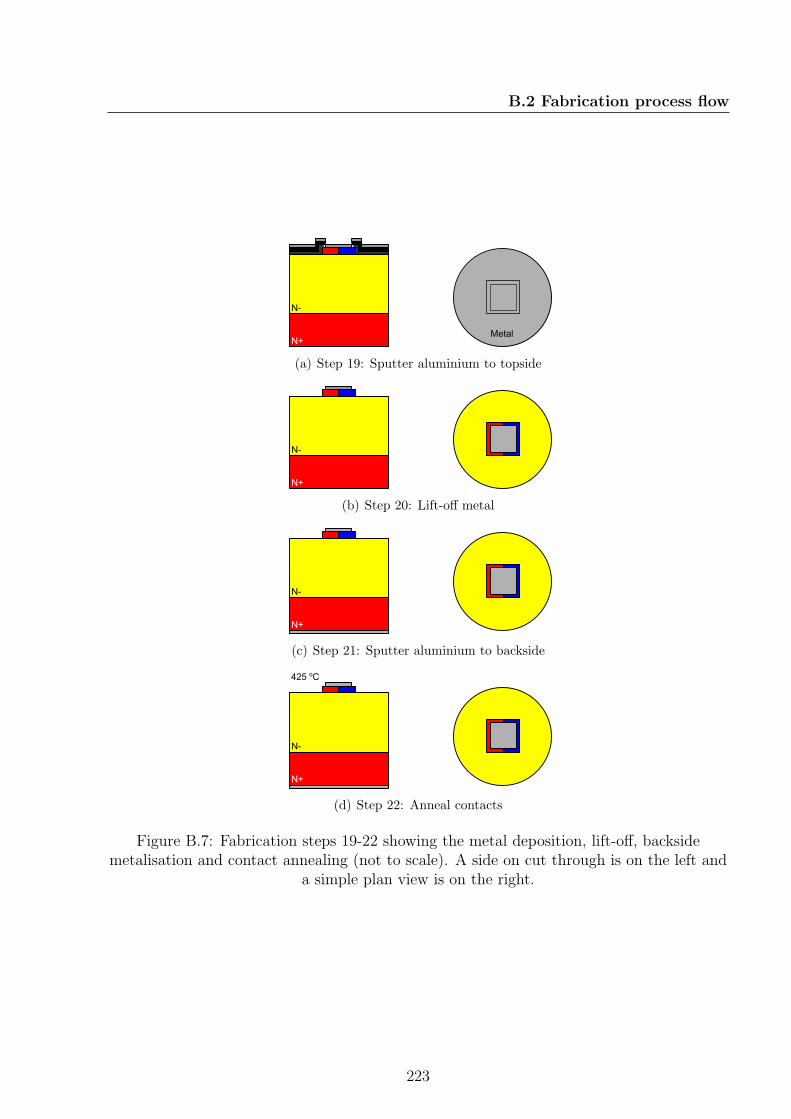
B.2 Fabrication process flow
N+
N-
Metal
(a) Step 19: Sputter aluminium to topside
N+
N-
(b) Step 20: Lift-off metal
N+
N-
(c) Step 21: Sputter aluminium to backside
N+
N-
425 oC
(d) Step 22: Anneal contacts
Figure B.7: Fabrication steps 19-22 showing the metal deposition, lift-off, backsidemetalisation and contact annealing (not to scale). A side on cut through is on the left and
a simple plan view is on the right.
223

Appendix
C Simulated and Measured IV data
In this appendix the raw probe station data and individual simulated IV curves are reported
for completeness. Each fabricated device was measured from −5 V to +5 V . The majority
of devices showed a very high level of uniformity across the repetitions across the wafer.
However, there was some diversion in some of the repetitions of devices Fab 04, Fab 07b and
Fab 13 in the reverse characteristic as seen in figures C.3(d), C.3(i) and C.4(h). The area
of interest for this work was the forward characteristic of the devices so this discrepency
has not been investigated. As it is not consistent across all repetitions this charactereistic
is likely to be the result of a fabrication defect. It should still be considered in future work
however, to ensure it is not an inherent flaw in the device design. One of the iterations of
Fab 28 had an unusually high RDS(on). This was a simple manufacturing defect.
224
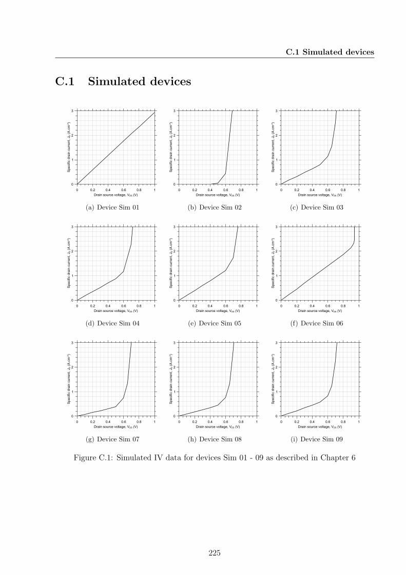
C.1 Simulated devices
C.1 Simulated devices
Specific drain current, JD (A.cm
-2)
0
1
2
3
Drain source voltage, VDS (V)
0 0.2 0.4 0.6 0.8 1
(a) Device Sim 01
Specific drain current, JD (A.cm
-2)
0
1
2
3
Drain source voltage, VDS (V)
0 0.2 0.4 0.6 0.8 1
(b) Device Sim 02
Specific drain current, JD (A.cm
-2)
0
1
2
3
Drain source voltage, VDS (V)
0 0.2 0.4 0.6 0.8 1
(c) Device Sim 03
Specific drain current, JD (A.cm
-2)
0
1
2
3
Drain source voltage, VDS (V)
0 0.2 0.4 0.6 0.8 1
(d) Device Sim 04
Specific drain current, JD (A.cm
-2)
0
1
2
3
Drain source voltage, VDS (V)
0 0.2 0.4 0.6 0.8 1
(e) Device Sim 05
Specific drain current, JD (A.cm
-2)
0
1
2
3
Drain source voltage, VDS (V)
0 0.2 0.4 0.6 0.8 1
(f) Device Sim 06
Specific drain current, JD (A.cm
-2)
0
1
2
3
Drain source voltage, VDS (V)
0 0.2 0.4 0.6 0.8 1
(g) Device Sim 07
Specific drain current, JD (A.cm
-2)
0
1
2
3
Drain source voltage, VDS (V)
0 0.2 0.4 0.6 0.8 1
(h) Device Sim 08
Specific drain current, JD (A.cm
-2)
0
1
2
3
Drain source voltage, VDS (V)
0 0.2 0.4 0.6 0.8 1
(i) Device Sim 09
Figure C.1: Simulated IV data for devices Sim 01 - 09 as described in Chapter 6
225
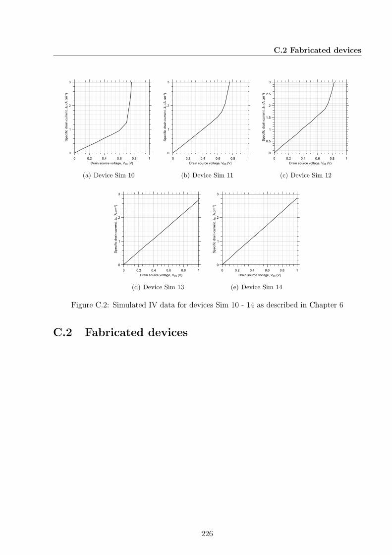
C.2 Fabricated devices
Specific drain current, JD (A.cm
-2)
0
1
2
3
Drain source voltage, VDS (V)
0 0.2 0.4 0.6 0.8 1
(a) Device Sim 10
Specific drain current, JD (A.cm
-2)
0
1
2
3
Drain source voltage, VDS (V)
0 0.2 0.4 0.6 0.8 1
(b) Device Sim 11
Specific drain current, J
D (A.cm
-2)
0
0.5
1
1.5
2
2.5
3
Drain source voltage, VDS (V)
0 0.2 0.4 0.6 0.8 1
(c) Device Sim 12
Specific drain current, JD (A.cm
-2)
0
1
2
3
Drain source voltage, VDS (V)
0 0.2 0.4 0.6 0.8 1
(d) Device Sim 13
Specific drain current, JD (A.cm
-2)
0
1
2
3
Drain source voltage, VDS (V)
0 0.2 0.4 0.6 0.8 1
(e) Device Sim 14
Figure C.2: Simulated IV data for devices Sim 10 - 14 as described in Chapter 6
C.2 Fabricated devices
226
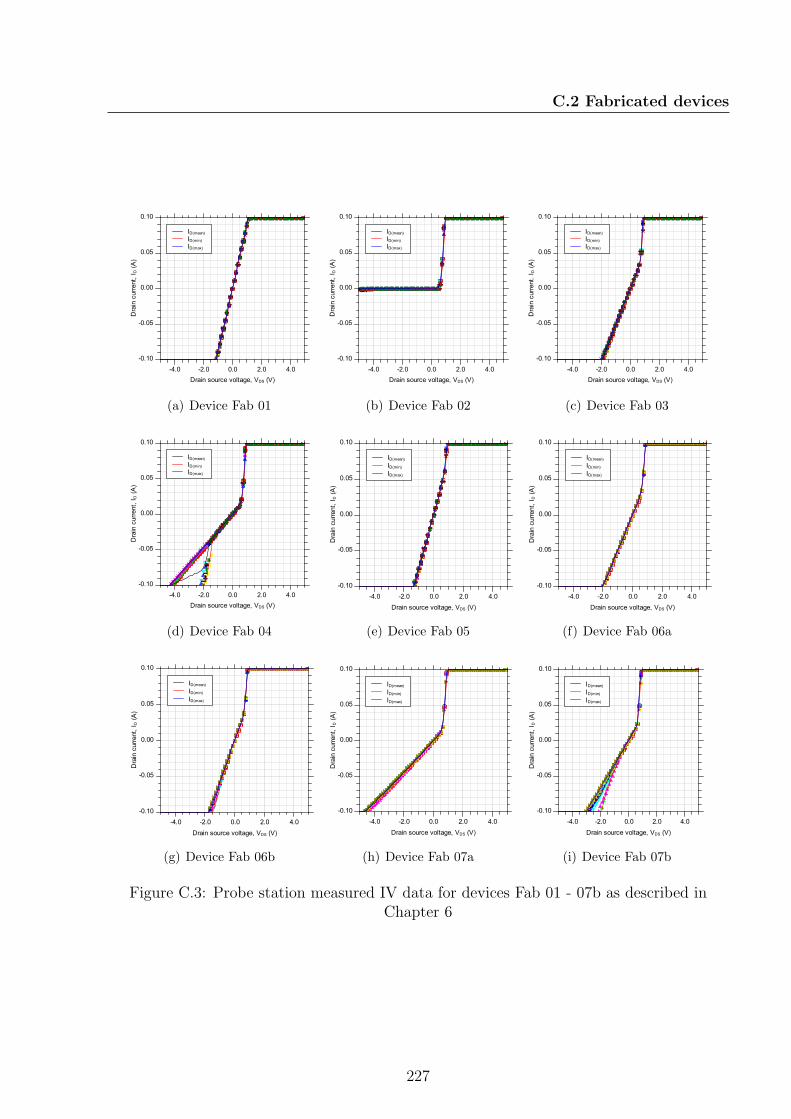
C.2 Fabricated devices
Drain current, ID (A)
-0.10
-0.05
0.00
0.05
0.10
Drain source voltage, VDS (V)
-4.0 -2.0 0.0 2.0 4.0
ID(mean)ID(min)ID(max)
(a) Device Fab 01
Drain current, ID (A)
-0.10
-0.05
0.00
0.05
0.10
Drain source voltage, VDS (V)
-4.0 -2.0 0.0 2.0 4.0
ID(mean)ID(min)ID(max)
(b) Device Fab 02
Drain current. ID (A)
-0.10
-0.05
0.00
0.05
0.10
Drain source voltage, VDS (V)
-4.0 -2.0 0.0 2.0 4.0
ID(mean)ID(min)ID(max)
(c) Device Fab 03
Drain current, ID (A)
-0.10
-0.05
0.00
0.05
0.10
Drain source voltage, VDS (V)
-4.0 -2.0 0.0 2.0 4.0
ID(mean)ID(min)ID(max)
(d) Device Fab 04
Drain current, ID (A)
-0.10
-0.05
0.00
0.05
0.10
Drain source voltage, VDS (V)
-4.0 -2.0 0.0 2.0 4.0
ID(mean)ID(min)ID(max)
(e) Device Fab 05
Drain current, ID (A)
-0.10
-0.05
0.00
0.05
0.10
Drain source voltage, VDS (V)
-4.0 -2.0 0.0 2.0 4.0
ID(mean)ID(min)ID(max)
(f) Device Fab 06a
Drain current, ID (A)
-0.10
-0.05
0.00
0.05
0.10
Drain source voltage, VDS (V)
-4.0 -2.0 0.0 2.0 4.0
ID(mean)ID(min)ID(max)
(g) Device Fab 06b
Drain current, ID (A)
-0.10
-0.05
0.00
0.05
0.10
Drain source voltage, VDS (V)
-4.0 -2.0 0.0 2.0 4.0
ID(mean)ID(min)ID(max)
(h) Device Fab 07a
Drain current, ID (A)
-0.10
-0.05
0.00
0.05
0.10
Drain source voltage, VDS (V)
-4.0 -2.0 0.0 2.0 4.0
ID(mean)ID(min)ID(max)
(i) Device Fab 07b
Figure C.3: Probe station measured IV data for devices Fab 01 - 07b as described inChapter 6
227
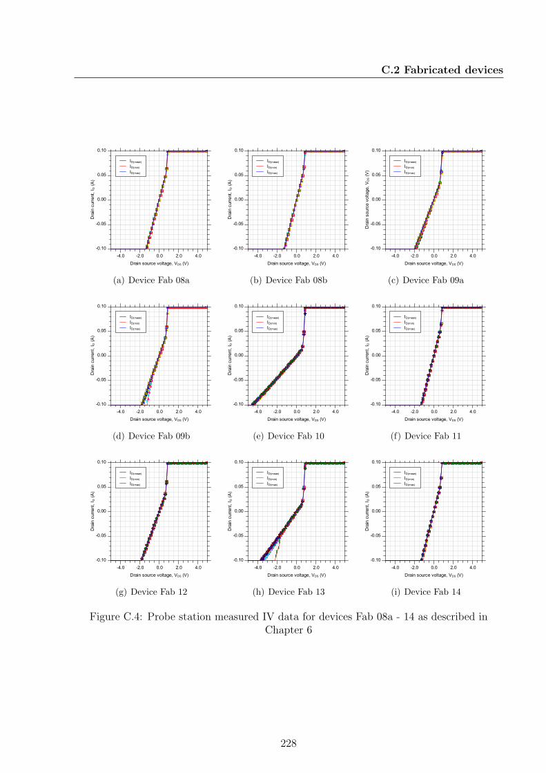
C.2 Fabricated devices
Drain current, ID (A)
-0.10
-0.05
0.00
0.05
0.10
Drain source voltage, VDS (V)
-4.0 -2.0 0.0 2.0 4.0
ID(mean)ID(min)ID(max)
(a) Device Fab 08a
Drain current, ID (A)
-0.10
-0.05
0.00
0.05
0.10
Drain source voltage, VDS (V)
-4.0 -2.0 0.0 2.0 4.0
ID(mean)ID(min)ID(max)
(b) Device Fab 08b
Drain source voltage, VDS (V)
-0.10
-0.05
0.00
0.05
0.10
Drain source voltage, VDS (V)
-4.0 -2.0 0.0 2.0 4.0
ID(mean)ID(min)ID(max)
(c) Device Fab 09a
Drain current, ID (A)
-0.10
-0.05
0.00
0.05
0.10
Drain source voltage, VDS (V)
-4.0 -2.0 0.0 2.0 4.0
ID(mean)ID(min)ID(max)
(d) Device Fab 09b
Drain current, ID (A)
-0.10
-0.05
0.00
0.05
0.10
Drain source voltage, VDS (V)
-4.0 -2.0 0.0 2.0 4.0
ID(mean)ID(min)ID(max)
(e) Device Fab 10
Drain current, ID (A)
-0.10
-0.05
0.00
0.05
0.10
Drain source voltage, VDS (V)
-4.0 -2.0 0.0 2.0 4.0
ID(mean)ID(min)ID(max)
(f) Device Fab 11
Drain current, ID (A)
-0.10
-0.05
0.00
0.05
0.10
Drain source voltage, VDS (V)
-4.0 -2.0 0.0 2.0 4.0
ID(mean)ID(min)ID(max)
(g) Device Fab 12
Drain current, ID (A)
-0.10
-0.05
0.00
0.05
0.10
Drain source voltage, VDS (V)
-4.0 -2.0 0.0 2.0 4.0
ID(mean)ID(min)ID(max)
(h) Device Fab 13
Drain current, ID (A)
-0.10
-0.05
0.00
0.05
0.10
Drain source voltage, VDS (V)
-4.0 -2.0 0.0 2.0 4.0
ID(mean)ID(min)ID(max)
(i) Device Fab 14
Figure C.4: Probe station measured IV data for devices Fab 08a - 14 as described inChapter 6
228
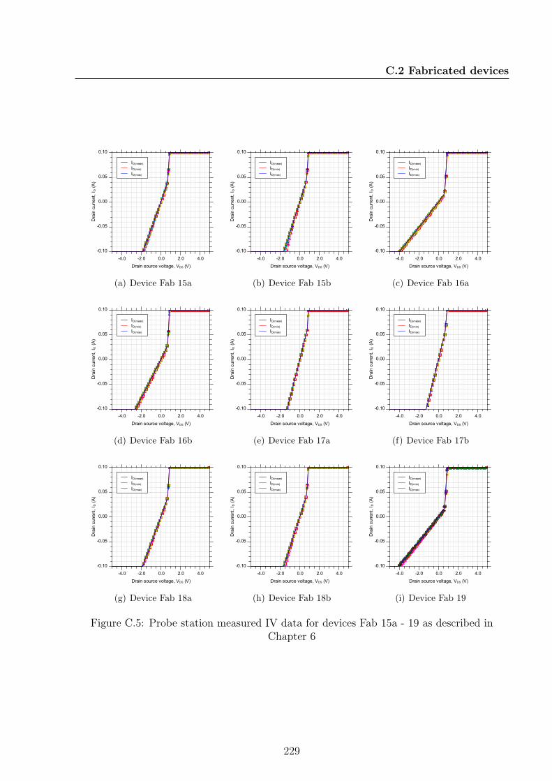
C.2 Fabricated devices
Drain current, ID (A)
-0.10
-0.05
0.00
0.05
0.10
Drain source voltage, VDS (V)
-4.0 -2.0 0.0 2.0 4.0
ID(mean)ID(min)ID(max)
(a) Device Fab 15a
Drain current, ID (A)
-0.10
-0.05
0.00
0.05
0.10
Drain source voltage, VDS (V)
-4.0 -2.0 0.0 2.0 4.0
ID(mean)ID(min)ID(max)
(b) Device Fab 15b
Drain current, ID (A)
-0.10
-0.05
0.00
0.05
0.10
Drain source voltage, VDS (V)
-4.0 -2.0 0.0 2.0 4.0
ID(mean)ID(min)ID(max)
(c) Device Fab 16a
Drain current, ID (A)
-0.10
-0.05
0.00
0.05
0.10
Drain source voltage, VDS (V)
-4.0 -2.0 0.0 2.0 4.0
ID(mean)ID(min)ID(max)
(d) Device Fab 16b
Drain current, ID (A)
-0.10
-0.05
0.00
0.05
0.10
Drain source voltage, VDS (V)
-4.0 -2.0 0.0 2.0 4.0
ID(mean)ID(min)ID(max)
(e) Device Fab 17a
Drain current, ID (A)
-0.10
-0.05
0.00
0.05
0.10
Drain source voltage, VDS (V)
-4.0 -2.0 0.0 2.0 4.0
ID(mean)ID(min)ID(max)
(f) Device Fab 17b
Drain current, ID (A)
-0.10
-0.05
0.00
0.05
0.10
Drain source voltage, VDS (V)
-4.0 -2.0 0.0 2.0 4.0
ID(mean)ID(min)ID(max)
(g) Device Fab 18a
Drain current, ID (A)
-0.10
-0.05
0.00
0.05
0.10
Drain source voltage, VDS (V)
-4.0 -2.0 0.0 2.0 4.0
ID(mean)ID(min)ID(max)
(h) Device Fab 18b
Drain current, ID (A)
-0.10
-0.05
0.00
0.05
0.10
Drain source voltage, VDS (V)
-4.0 -2.0 0.0 2.0 4.0
ID(mean)ID(min)ID(max)
(i) Device Fab 19
Figure C.5: Probe station measured IV data for devices Fab 15a - 19 as described inChapter 6
229
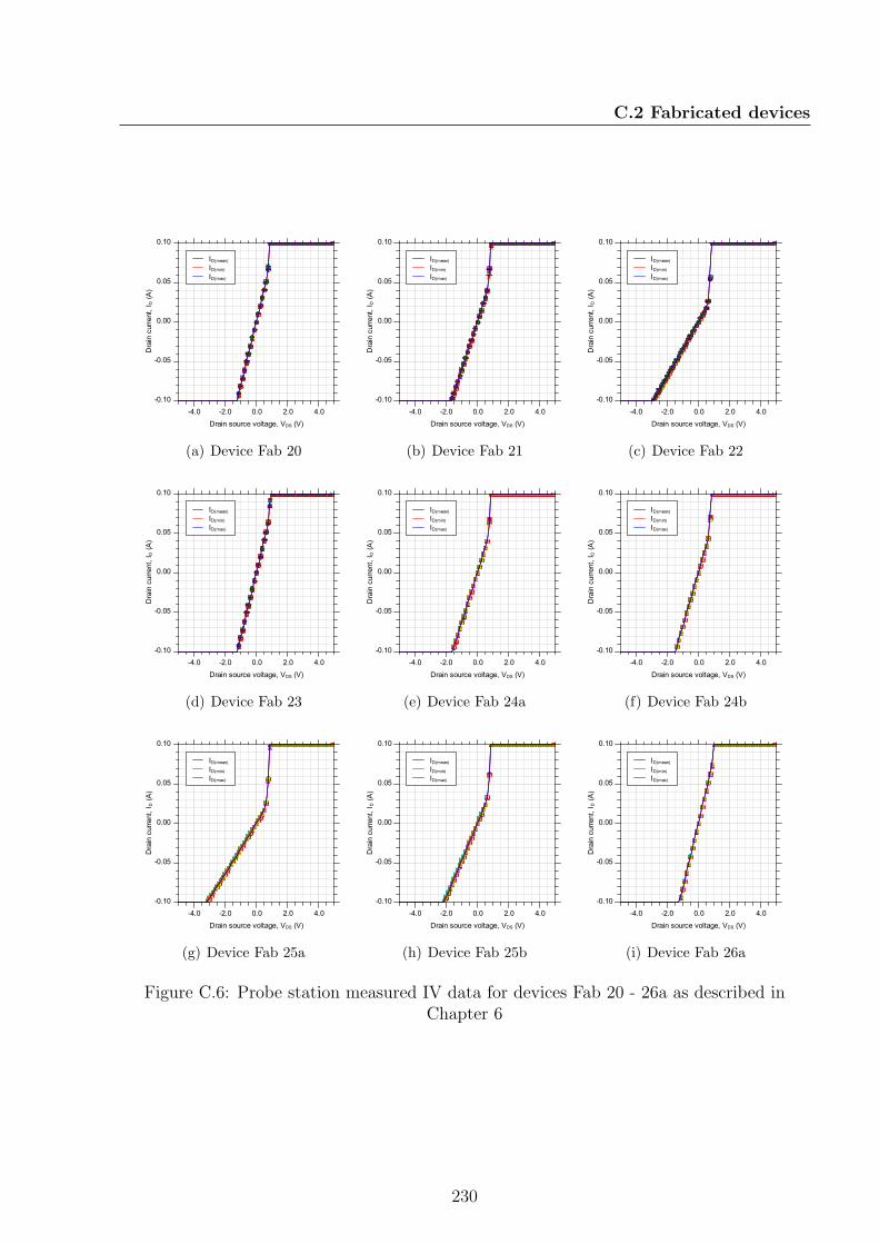
C.2 Fabricated devices
Drain current, ID (A)
-0.10
-0.05
0.00
0.05
0.10
Drain source voltage, VDS (V)
-4.0 -2.0 0.0 2.0 4.0
ID(mean)ID(min)ID(max)
(a) Device Fab 20
Drain current, ID (A)
-0.10
-0.05
0.00
0.05
0.10
Drain source voltage, VDS (V)
-4.0 -2.0 0.0 2.0 4.0
ID(mean)ID(min)ID(max)
(b) Device Fab 21
Drain current, ID (A)
-0.10
-0.05
0.00
0.05
0.10
Drain source voltage, VDS (V)
-4.0 -2.0 0.0 2.0 4.0
ID(mean)ID(min)ID(max)
(c) Device Fab 22
Drain current, ID (A)
-0.10
-0.05
0.00
0.05
0.10
Drain source voltage, VDS (V)
-4.0 -2.0 0.0 2.0 4.0
ID(mean)ID(min)ID(max)
(d) Device Fab 23
Drain current, ID (A)
-0.10
-0.05
0.00
0.05
0.10
Drain source voltage, VDS (V)
-4.0 -2.0 0.0 2.0 4.0
ID(mean)ID(min)ID(max)
(e) Device Fab 24a
Drain current, ID (A)
-0.10
-0.05
0.00
0.05
0.10
Drain source voltage, VDS (V)
-4.0 -2.0 0.0 2.0 4.0
ID(mean)ID(min)ID(max)
(f) Device Fab 24b
Drain current, ID (A)
-0.10
-0.05
0.00
0.05
0.10
Drain source voltage, VDS (V)
-4.0 -2.0 0.0 2.0 4.0
ID(mean)ID(min)ID(max)
(g) Device Fab 25a
Drain current, ID (A)
-0.10
-0.05
0.00
0.05
0.10
Drain source voltage, VDS (V)
-4.0 -2.0 0.0 2.0 4.0
ID(mean)ID(min)ID(max)
(h) Device Fab 25b
Drain current, ID (A)
-0.10
-0.05
0.00
0.05
0.10
Drain source voltage, VDS (V)
-4.0 -2.0 0.0 2.0 4.0
ID(mean)ID(min)ID(max)
(i) Device Fab 26a
Figure C.6: Probe station measured IV data for devices Fab 20 - 26a as described inChapter 6
230
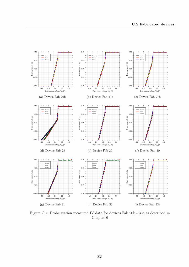
C.2 Fabricated devices
Drain current, ID (A)
-0.10
-0.05
0.00
0.05
0.10
Drain source voltage, VDS (V)
-4.0 -2.0 0.0 2.0 4.0
ID(mean)ID(min)ID(max)
(a) Device Fab 26b
Drain current, ID (A)
-0.10
-0.05
0.00
0.05
0.10
Drain source voltage, VDS (V)
-4.0 -2.0 0.0 2.0 4.0
ID(mean)ID(min)ID(max)
(b) Device Fab 27a
Drain current, ID (A)
-0.10
-0.05
0.00
0.05
0.10
Drain source voltage, VDS (V)
-4.0 -2.0 0.0 2.0 4.0
ID(mean)ID(min)ID(max)
(c) Device Fab 27b
Drain current, ID (A)
-0.10
-0.05
0.00
0.05
0.10
Drain source voltage, VDS (V)
-4.0 -2.0 0.0 2.0 4.0
ID(mean)ID(min)ID(max)
(d) Device Fab 28
Drain current, ID (A)
-0.10
-0.05
0.00
0.05
0.10
Drain source voltage, VDS (V)
-4.0 -2.0 0.0 2.0 4.0
ID(mean)ID(min)ID(max)
(e) Device Fab 29
Drain current, ID (A)
-0.10
-0.05
0.00
0.05
0.10
Drain source voltage, VDS (V)
-4.0 -2.0 0.0 2.0 4.0
ID(mean)ID(min)ID(max)
(f) Device Fab 30
Drain current, ID (A)
-0.10
-0.05
0.00
0.05
0.10
Drain source voltage, VDS (V)
-4.0 -2.0 0.0 2.0 4.0
ID(mean)ID(min)ID(max)
(g) Device Fab 31
Drain current, ID (A)
-0.10
-0.05
0.00
0.05
0.10
Drain source voltage, VDS (V)
-4.0 -2.0 0.0 2.0 4.0
ID(mean)ID(min)ID(max)
(h) Device Fab 32
Drain current, ID (A)
-0.10
-0.05
0.00
0.05
0.10
Drain source voltage, VDS (V)
-4.0 -2.0 0.0 2.0 4.0
ID(mean)ID(min)ID(max)
(i) Device Fab 33a
Figure C.7: Probe station measured IV data for devices Fab 26b - 33a as described inChapter 6
231
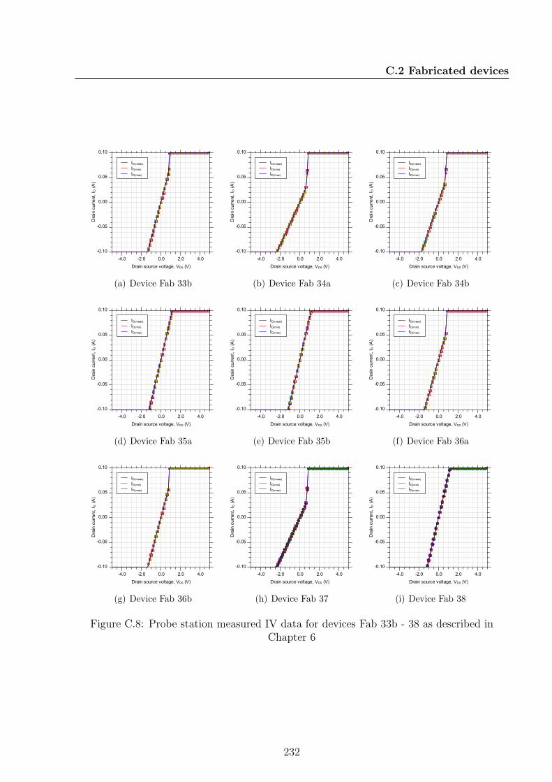
C.2 Fabricated devices
Drain current, ID (A)
-0.10
-0.05
0.00
0.05
0.10
Drain source voltage, VDS (V)
-4.0 -2.0 0.0 2.0 4.0
ID(mean)ID(min)ID(max)
(a) Device Fab 33b
Drain current, ID (A)
-0.10
-0.05
0.00
0.05
0.10
Drain source voltage, VDS (V)
-4.0 -2.0 0.0 2.0 4.0
ID(mean)ID(min)ID(max)
(b) Device Fab 34a
Drain current, ID (A)
-0.10
-0.05
0.00
0.05
0.10
Drain source voltage, VDS (V)
-4.0 -2.0 0.0 2.0 4.0
ID(mean)ID(min)ID(max)
(c) Device Fab 34b
Drain current, ID (A)
-0.10
-0.05
0.00
0.05
0.10
Drain source voltage, VDS (V)
-4.0 -2.0 0.0 2.0 4.0
ID(mean)ID(min)ID(max)
(d) Device Fab 35a
Drain current, ID (A)
-0.10
-0.05
0.00
0.05
0.10
Drain source voltage, VDS (V)
-4.0 -2.0 0.0 2.0 4.0
ID(mean)ID(min)ID(max)
(e) Device Fab 35b
Drain current, ID (A)
-0.10
-0.05
0.00
0.05
0.10
Drain source voltage, VDS (V)
-4.0 -2.0 0.0 2.0 4.0
ID(mean)ID(min)ID(max)
(f) Device Fab 36a
Drain current, ID (A)
-0.10
-0.05
0.00
0.05
0.10
Drain source voltage, VDS (V)
-4.0 -2.0 0.0 2.0 4.0
ID(mean)ID(min)ID(max)
(g) Device Fab 36b
Drain current, ID (A)
-0.10
-0.05
0.00
0.05
0.10
Drain source voltage, VDS (V)
-4.0 -2.0 0.0 2.0 4.0
ID(mean)ID(min)ID(max)
(h) Device Fab 37
Drain current, ID (A)
-0.10
-0.05
0.00
0.05
0.10
Drain source voltage, VDS (V)
-4.0 -2.0 0.0 2.0 4.0
ID(mean)ID(min)ID(max)
(i) Device Fab 38
Figure C.8: Probe station measured IV data for devices Fab 33b - 38 as described inChapter 6
232
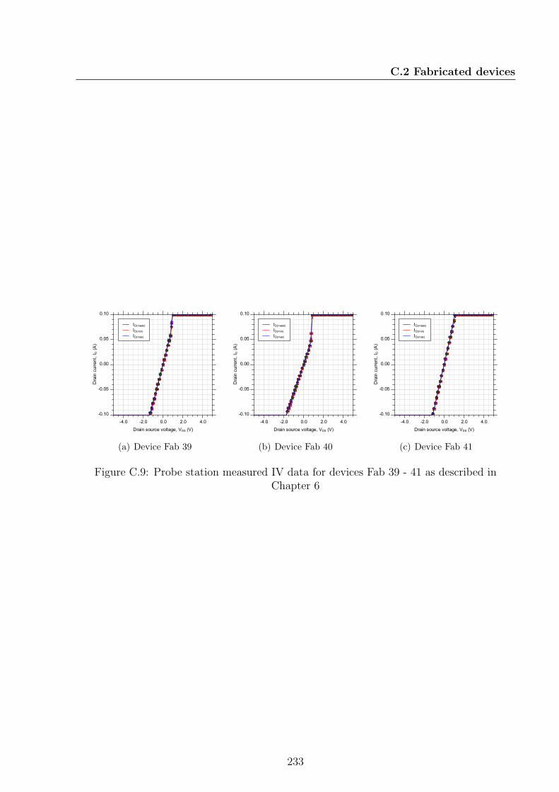
C.2 Fabricated devices
Drain current, ID (A)
-0.10
-0.05
0.00
0.05
0.10
Drain source voltage, VDS (V)
-4.0 -2.0 0.0 2.0 4.0
ID(mean)ID(min)ID(max)
(a) Device Fab 39
Drain current, ID (A)
-0.10
-0.05
0.00
0.05
0.10
Drain source voltage, VDS (V)
-4.0 -2.0 0.0 2.0 4.0
ID(mean)ID(min)ID(max)
(b) Device Fab 40
Drain current, ID (A)
-0.10
-0.05
0.00
0.05
0.10
Drain source voltage, VDS (V)
-4.0 -2.0 0.0 2.0 4.0
ID(mean)ID(min)ID(max)
(c) Device Fab 41
Figure C.9: Probe station measured IV data for devices Fab 39 - 41 as described inChapter 6
233
Appendix
D Publications
D.1 Publications arising from this Thesis
D.1.1 International conference publications
1. B. T. Donnellan, P .A. Mawby, M. Rahimo, L. Storasta “Introducing a 1200 V
Vertical Merged IGBT and Power MOSFET: The HUBFET”Applied Power Electronics
Conference and Exposition (APEC) 2012, Orlando, Florida, USA
D.2 Other publications by the author
D.2.1 Journal publications
1. B. T. Donnellan, G. J. Roberts, P. A. Mawby, A. T. Bryant “Modelling of current
sharing in paralleled current limiting superjunction MOSFETS with common gate
drives”Microelectronics Reliability - Vol. 52, Issue 3, pp. 497 - 502, 2012
234

D.2 Other publications by the author
2. M. R. Jennings, A. Perez-Tomas, A. Bashir, A. Sanchez, A. Severino, P. J. Ward,
S. M. Thomas, C. Fisher, P. M. Gammon, M. Zabala, S. E. Burrows, B. T. Donnellan,
D. P. Hamilton, D. Walker, P. A. Mawby “Bow free 4 diameter 3C-SiC epilayers formed
upon wafer-bonded Si/SiC substrates”ECS Solid State Letters, Vol. 1, No. 6, pp.
85 88, 2012
D.2.2 International conference publications
1. B. T. Donnellan, P. A. Mawby, A. T. Bryant “Modelling of current sharing in paral-
leled current limiting superjunction MOSFETS with common gate drives”International
Seminar on Power Semiconductors (ISPS) 2010 Prague, Czech Republic
2. K. K. Leong, B. T. Donnellan, A. T. Bryant, P. A. Mawby “An investigation into the
utilisation of power MOSFETs at cryogenic temperatures to achieve ultra-low power
losses”Energy Conversion Congress and Exposition (ECCE) 2010, Atlanta, Georgia,
USA
3. M. R. Jennings, A. Perez-Tomas, A. Severino, P. J. Ward, A. Bashir, C. Fisher,
S. M. Thomas, P. M. Gammon,B. T. Donnellan, H. Rong, D. P. Hamilton, P. A. Mawby
“Innovative 3C-SiC on SiC via Direct Wafer Bonding”European Conference on Silicon
Carbide and Related Materials (ECSCRM) 2012, St. Petersburg, Russia
4. P. M. Gammon, A. Perez-Tomas, M. R. Jennings, A. Sanchez, C. Fisher, S. M. Thomas,
B. T. Donnellan, P. A. Mawby “Bipolar conduction across a wafer bonded p-n
Si/SiC heterojunction”European Conference on Silicon Carbide and Related Materials
235

D.2 Other publications by the author
(ECSCRM) 2012, St. Petersburg, Russia
236