Embed Size (px)
Citation preview
UNIVERSITY OF OVIEDO
DESIGN AND DEVELOPMENT OF 20KW BIDIRECTIONAL DC-DC
CONVERTER USING SILICON CARBIDE TECHNOLOGY by
Abduselam Hamid Beshir
(email: [email protected])
Thesis submitted in partial fulfilment of the requirements for Erusmus Mundus
joint Master’s degree in sustainable transportation and Electrical power system
at
The University of Oviedo
Department of Electrical, Electronic, Computer and Systems Engineering
August, 2019
Main Advisor: Fernando Briz …………………………
Full professor Signature
Department of Electrical, Electronic, Computer and Systems Engineering
University of Oviedo, Gijon, Spain
Co –Advisor: Carlos Martinez de Guerenu ……………………
Director of R&D Department Signature
Zigor Corporation, Vitoria Gasteiz, Spain

i
ABSTRACT
This Master’s thesis presents the design and prototype development of a 20KW Bidirectional
DC-DC converter using silicon Carbide MOSFETs. The first part of this thesis presents the
theoretical background of SiC material and SiC MOSFETs. This is followed by general
theory on Bidirectional DC-DC converters. Subsequently the step by step procedures and
design consideration of Power stage, Driver circuit and the Control system of the
Bidirectional DC-DC converter is discussed briefly. In power stage design, Silicon carbide
MOSFETs from different manufacturers (WOLFSPEED and UNITED SILICON CARBIDE)
are compared. Moreover the details of selection and sizing of SiC MOSFETs, capacitors,
resistors, inductors and the heatsink is presented in detail. The gate driver circuit is
appropriately designed so that the Bidirectional DC-DC converter can work for both
UF3C120040K4S, United Silicon Carbide MOSFETs and C3M003090K, Wolfspeed Cree
third generation SiC MOSFETs. In addition to this Average Current Control technique is
used for controlling the inductor current. The schematics and PCB of the DC-DC converter
has been made using Cadstar Software. Moreover the components are mounted properly and
prototype is developed. The Bidirectional DC-DC converter is tested for operation. Firstly a
laboratory circuit enabling double-pulse test is built and the switching behaviour of
UF3C120040K4S and C3M003090K SiC MOSFETs are analysed. Next to this the
Bidirectional DC-DC converter is tested for BOOST and BUCK operation. Finally results
from software simulation and laboratory experiment are presented in detail.

ii
ACKNOWLEDGMENT
First I would like to express my sincere gratitude towards my main Supervisor Prof.
Fernando Briz for his advice and guidance. Next I would like to use this opportunity to thank
Mr. Carlos Martinez de Guerenu. It is really once a life time opportunity to work with him
and I really appreciate his attitude, guidance and support. He has constantly encouraged and
supported me from the beginning of the project to the end. His observations and comments
helped me to establish the overall direction of the research and to move forward with
investigation in depth. He helped me a lot and been a source of knowledge.
I would like to thank Jose Felix and Jose Antonio for their help on the Schematics and PCB
design. I would like to take this opportunity also to thank all the R&D department members
at Zigor Corporation Eneko, Jorge, Alvaro, Sebastian, Asier, Sergio, Feliciano, Igor and
Giorgio for their love, support and encouragement.
Lastly I would like to thank all the administrative and technical staffs at Zigor Corporation
for their support and guidance.

iii
DEDICATION
To
My beloved Wife Sumeya Mahmoud Teyib
And
My Grandmother Temima Mehdi Helifa

iv
CONTENTS
ABSTRACT ................................................................................................................................ i
ACKNOWLEDGMENT............................................................................................................ ii
DEDICATION ......................................................................................................................... iii
ABBREVIATIONS .................................................................................................................. ix
CHAPTER ONE ........................................................................................................................ 1
1. INTRODUCTION ................................................................................................................. 1
1.1 Background ...................................................................................................................... 1
1.2 Objectives and Deliverables ............................................................................................. 2
1.3 Structure of the Report ..................................................................................................... 3
CHAPTER 2 .............................................................................................................................. 4
2. STATE OF THE ART OF SIC MOSFETs AND BIDIRECTIONAL DC-DC
CONVERTERS ......................................................................................................................... 4
2.1 Silicon Carbide semiconductor ........................................................................................ 4
2.1.1 Material properties and advantages ........................................................................... 4
2.2 Basic Structure Of SiC MOSFETs ................................................................................... 5
2.2.1 SiC MOSFET Parasitic Capacitance ......................................................................... 6
2.3 Characteristics of SiC MOSFETS .................................................................................... 8
2.3.1 Gate driver voltage Vgs and Rdson ........................................................................... 8
2.3.2 Vds-Id characteristics ................................................................................................ 9
2.3.3 SiC MOSFET Switching Characteristics ................................................................ 11
2.3.3.1Turn-On Switching Characteristics.................................................................... 11
2.3.3.2 Turn-Off Switching Characteristics .................................................................. 12
2.3.3.3 Switching and conduction loss of SiC MOSFET ............................................. 12
2.4. Bidirectional DC-DC converters ................................................................................... 15
2.4.1 Non-isolated BDC ................................................................................................... 15
2.4.2 Isolated BDC (IBDC) .............................................................................................. 16
2.5 Summary ........................................................................................................................ 18
CHAPTER THREE ................................................................................................................. 19
3. CONVERTER DESIGN METHODOLOGY ...................................................................... 19
3.1 Power Circuit Design Steps ........................................................................................... 19
3.2 Heat Sink Design ............................................................................................................ 20
3.3 Driver circuit design steps and considerations ............................................................... 21
3.3.1 Wide range of Gate voltages ................................................................................... 22

v
3.3.2 Output current Requirement .................................................................................... 23
3.3.3 Input-Output Delay Time ........................................................................................ 23
3.3.4 Other considerations ................................................................................................ 23
3.4 Control system design .................................................................................................... 24
3.4.1 Voltage mode control (VMC) .................................................................................. 24
3.4.2 Current mode control (CMC) .................................................................................. 24
3.4.2.1 Peak Current Mode Control .............................................................................. 25
3.4.2.2 Average Current Mode Control ........................................................................ 26
3.4.3 MOSFET Dead Time ............................................................................................... 26
3.5 PCB design considerations ............................................................................................. 27
CHAPTER FOUR .................................................................................................................... 29
4. CASE –STUDY ................................................................................................................... 29
4.1 Power circuit Design ...................................................................................................... 29
4.1.1 Choosing SiC MOSFETs......................................................................................... 29
4.1.2. Selecting Switching frequency, the required inductor, Capacitors and Heat sink . 30
4.2 Driver circuit design ....................................................................................................... 33
4.3. Control circuit design .................................................................................................... 35
4.3.1 Current loop design ................................................................................................. 35
4.3.2 Voltage loop Design ................................................................................................ 36
4.3.3 Dead time circuit ..................................................................................................... 37
4.4. PCB design .................................................................................................................... 37
4.5 Double pulse test Set Up ................................................................................................ 38
4.6. Software simulation....................................................................................................... 43
4.7 Summary ........................................................................................................................ 48
CHAPTER 5 ............................................................................................................................ 49
5. RESULT AND DISCUSSION ............................................................................................ 49
5.1 Measuring Instruments ................................................................................................... 49
5.2 Power supplies................................................................................................................ 49
5.3 Testing the Gate driver Circuit ....................................................................................... 50
5.4 Testing the dead time Generating Circuit ...................................................................... 51
5.5 Double Pulse Test........................................................................................................... 53
5.6 Testing the operation of the DC-DC converter .............................................................. 57
5.6.1 Boost Operation ....................................................................................................... 57

vi
5.6.2 Buck Operation ........................................................................................................ 58
CHAPTER 6 ............................................................................................................................ 60
6. CONCLUSION AND FUTURE WORK ............................................................................ 60
6.1 Conclusion ........................................................................................................................ 60
6.2 Future Work ..................................................................................................................... 60
REFERENCES ........................................................................................................................ 62

vii
LIST OF TABLES
Table 2. 1 Main properties of Si and SiC[27] ........................................................................................ 5
Table 3. 1 Gate to source voltage limits for different SiC MOSFETs..……………………………….23
Table 4.1 Comparison of switching energy loses for Different types of SiCMOSFETs……………...30
Table 4. 2 Size of inductor for various frequencies .............................................................................. 30
Table 4.3 Double pulse generator circuit reference values of resistors and capacitors for required time
values .................................................................................................................................................... 42
LIST OF FIGURES
Figure 2. 1 Basic structure of the n-channel DMOS MOSFET[27] ....................................................... 5
Figure 2. 2 Power MOSFET structures[27] ............................................................................................ 6
Figure 2.3 Intrinsic capacitance in the n-channel DMOS MOSFET [27] .............................................. 7
Figure 2.4 Capacitance Vs Drain to source voltage Vds Cree C3M0065100K Silicon Carbide Power
MOSFET ................................................................................................................................................. 8
Figure 2.5 on resistance Vs. Temperature for various Gate Voltage of Cree C3M0065100K Silicon
Carbide Power MOSFET. ....................................................................................................................... 9
Figure 2.6 I-V characteristics of SiC MOSFET [27] ............................................................................ 10
Figure 2.7 Gate-to-Source voltage transfer characteristics[27] ............................................................ 10
Figure 2. 8 MOSFET gate charging and discharging equivalent circuit ............................................... 11
Figure 2. 9 Turn -on switching characteristics ...................................................................................... 11
Figure 2. 10 Turn –off switching characteristics .................................................................................. 12
Figure 2. 11 (a) Basic NBDC (b) operating waveforms ................................................................. 16
Figure 2.12 Basic structure of IBDC .................................................................................................... 17
Figure 2. 13 Dual Bridge Isolated Voltage Fed Bidirectional DC-DC Converter ................................ 17
Figure 3. 1 Bi directional Boost Converter……………………………………………..……………..19
Figure 3. 2 MOSFET current ................................................................................................................ 13
Figure 3. 3 (a) switching energy vs.External gate resistor (b) switching energy vs drain current ....... 14
Figure 3.4 Diagram of (a)cross-section of SiC device on heat sink and (b) thermal model ............. 20
Figure 3.5 Components of gate driver circuit ....................................................................................... 22
Figure 3. 6 (a) Peak current control scheme (b) average current control scheme ......................... 25
Figure 4.1 Designed inductor…………………………………………………………………………31
Figure 4.2 Heat sink thermal equivalent circuit .................................................................................... 32
Figure 4.3 Thermal Resistance Curve of CR Series Heat sink ............................................................. 33
Figure 4.4 Schematic circuit used to generate Dead time .................................................................... 37
Figure 4.5 (a) Double pulse test circuit (b) wave form of applied pulse ,transistor current and
inductor current ..................................................................................................................................... 38
Figure 4.6 Schematics of the power circuit and driver circuit of the DC-DC converter....................... 39
Figure 4.7 Top layer the PCB ............................................................................................................... 40
Figure 4.8 Bottom layer of the PCB ..................................................................................................... 40
Figure 4.9 DC-DC converter prototype ................................................................................................ 41
Figure 4.10 Schematics of double pulse generator circuit .................................................................... 42
Figure 4.11 LTspice Circuit Model of the DC-DC converter power circuit ......................................... 43
Figure 4.12 (a) inductor ripple current (b) input-output voltage of the DC- DC converter ........ 44
Figure 4.13 Vds vs.Ids graph of Cree C3M0065100K SiC during turn on.......................................... 44
Figure 4.14 Vds vs.Ids graph of Cree C3M0065100K SiC during turn off ......................................... 45
Figure 4.15 Simulink Model of Average current control scheme of the DC-DC converter ................. 45
Figure 4.16 Simulink model of current control loop............................................................................. 46

viii
Figure 4.17 Simulink model of voltage control loop ............................................................................ 46
Figure 4.18 Voltage loop Reference voltage and inductor current wave form ..................................... 47
Figure 4.19(a) Step voltage (b) Average current control loop simulation result showing
bidirectional control .............................................................................................................................. 47
Figure 4. 20 Low and High voltage side voltages .................................................................................. 48
Figure 5. 1 SUNZET 25KW DC Power supply………………………………………………………50
Figure 5. 2 Function generator set up ................................................................................................... 51
Figure 5. 3 (a) Gate Driver IC input-output wave form ( b) Gate Driver IC input-output delay ........ 51
Figure 5. 4 Dead time bread board circuit ............................................................................................ 52
Figure 5. 5 Upper and Lowe leg PWM signals ..................................................................................... 52
Figure 5. 6 Dead time between upper and lower leg PWM signals ...................................................... 53
Figure 5. 7 Double pulse waveform ...................................................................................................... 53
Figure 5. 8 Inductor current, Vgs and Vgd during double pulse test ................................................ 54
Figure 5.9 Vds and Vgs graphs during (a) Switch on transient (b) switch off transient at 30V test
voltage ................................................................................................................................................... 55
Figure 5. 10 Vds and Vgs graphs at 30V test voltage after snubber capacitor is added (a) Switch on
transient (b) switch off transient ........................................................................................................ 55
Figure 5. 11 Vds and Vgs voltage (a) Switch off transient at 500V test voltage (b) switch on transient
at 300V test voltage .............................................................................................................................. 56
Figure 5. 12 Inductor current at 700V test voltage during double pulse test ........................................ 56
Figure 5. 13 Boost Operation Test Set-Up ............................................................................................ 57
Figure 5. 14 Boost operation (a)30v to 58V (b)380V to 680 V ............................................................ 58
Figure 5. 15 Gate driver voltage and inductor current waveform ......................................................... 58
Figure 5. 16 Buck operation Set-Up ..................................................................................................... 59
Figure 5. 17 Buck operation (a)30V to 14V (b)380V to 180V .......................................................... 59

ix
ABBREVIATIONS
Acronym
AC
ADC
BDC
BJT
BOM
D
DC
DPT
DSP
DUT
EMC
EMI
ESR
FRD
fsw
GaN
HEV
IBDC
IC
IGBT
JFET
MOSFET
NBDC
PCB
PV
PWM
RMS
SBD
SCP
Si
SiC
SMD
Definition
Alternating Current
Analog to Digital Converter
Bidirectional DC-DC Converter
Bipolar Junction Transistor
Bill of Materials
Duty Cycle
Direct Current
Double-Pulse Test
Digital Signal Processor
Device Under Test
Electromagnetic Compatibility
Electromagnetic Interference
Equivalent Series Resistance
Fast-Recovery Diode
Switching Frequency
Gallium Nitride
Hybrid electric vehicles
Isolated Bi-directional DC-DC converters
Interconnected Circuit
Insulated-Gate Bipolar Transistor
Junction Gate Field-Effect Transistor
Metal-Oxide-Semiconductor Field-Effect Transistor
Non-isolated Bi-directional DC-DC converters
Printed Circuit Board
Photovoltaic
Pulse-Width Modulation
Root Mean Square
Schottky Barrier Diode
Short-Circuit Protection
Silicon
Silicon Carbide
Surface-Mount Device
1
CHAPTER ONE
1. INTRODUCTION
1.1 Background
In today’s world the energy sector is giving much attention to Renewable energy sources.
Renewable energy sources are clean and inexhaustible. However wind and solar energy are
intermittent in nature and they are unsuitable for standalone operation. They require smart
systems for their sustainable operation. One solution to this intermittency problem is to use
energy storage system along with such renewable energy sources to compensate fluctuations
and maintain a smooth and continuous power flow to the load. The energy storage system
stores excess energy and provide it at times of deficiency.
Smart power electronics converters with a capability of bidirectional power flow are required
in order to properly integrate an energy storage system, such as a battery bank and super
capacitors, along with a PV and wind installation. Bidirectional DC-DC converters (BDC)
have bidirectional power flow capability and they are getting much attention in systems
which require a two way power flow like energy storage application in renewable energy
systems, fuel cell energy systems, hybrid electric vehicles (HEV), dc motor drives and
uninterruptible power supplies (UPS) [3-5].
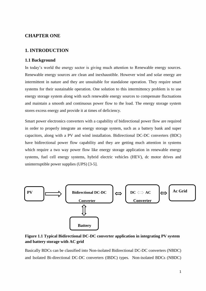
PV Bidirectional DC-DC DC AC
Converter Converter
Battery
Figure 1.1 Typical Bidirectional DC-DC converter application in integrating PV system
and battery storage with AC grid
Basically BDCs can be classified into Non-isolated Bidirectional DC-DC converters (NBDC)
and Isolated Bi-directional DC-DC converters (IBDC) types. Non-isolated BDCs (NBDC)
Ac Grid

2
are a derivation of normal boost type and buck type DC-DC converters by replacing diodes
by controllable power switches. Since they don´t have transformers for isolation purpose,
they have better efficiency, less size, less weight and low cost compared to IBDC and
applicable in systems where weight or size is the main concern. IBDC have transformer for
isolation system and voltage matching so that they are less efficient, more complex and have
higher weight and size. IBDC are preferable where system requires galvanic isolation [3].
The efficiency and size of the DC-DC converter is a great concern in today’s power
electronics applications. Silicon MOSFETs and IGBTs are used for most power electronics
converters at different power rating and voltage levels. However they are reaching their limit
in terms of switching frequency, efficiency, voltage rating and power density due to the
nature of the materials. Si-based power devices have limited performance related to inherent
material characteristics, which make them unable to meet future demands, especially in high-
voltage, high-efficiency, and high-power density applications. Wide Band Gap (WBG)
semiconductor materials, also known as the third generation semiconductor materials,
typically represented by Gallium Nitride (GaN), Aluminium Nitride (AlN) and Silicon
Carbide (SiC), are getting much attention in today’s Power electronic converters due to their
wide band gap nature, their high electron saturation velocity and high thermal conductivity.
These critical characteristics enable the power devices to operate at higher voltage, higher
temperature and higher switching frequencies than their Si-based counterparts and enable the
power converter applications to be lower in volume and higher efficiency [1-3].
In this thesis work the design and implementation of 20Kw Non Isolated Bidirectional DC-
DC converter using SiC technology is presented. Theoretical background of SiC MOSFETs
and DC-DC converters as well as different design consideration, software simulations and
laboratory experiment results are presented in the coming chapters
1.2 Objectives and Deliverables
The main objective of this thesis work is the design and prototype development of 20KW
Bidirectional DC-DC converter using SiC technology. The specific objective includes:
Design of Power stage of the Bidirectional DC-DC converter
Design of the driver circuit and control circuit
Prototype development and test the operation of the Bidirectional DC-DC converter

3
The main Deliverables of this thesis work are:
Simulation models
Complete DC-DC converter evaluation board
Project report including design procedures, Simulation results and experimental
results
1.3 Structure of the Report
Chapter Two explains the state of art of SiC MOSFETs and Bidirectional DC-DC converters.
Chapter 3 explains the methodology of the thesis work. In chapter four the detail design of
the DC-DC converter and software simulations are presented. Chapter five explains the
experimental results. Finally chapter six presents conclusion and recommendations.

4
CHAPTER 2
2. STATE OF THE ART OF SIC MOSFETs AND BIDIRECTIONAL DC-
DC CONVERTERS
2.1 Silicon Carbide semiconductor
2.1.1 Material properties and advantages
Power electronics is an enabling technology found in most renewable energy generation
systems. SiC has become the material of choice for next generation power semiconductor
devices to replace existing Si technology. It is a compound semiconductor comprised of
silicon (Si) and carbon (C). SiC has a band gap of three times higher than that of Si materials
and this results a number of advantages over conventional Si materials. The field strength of
SiC is around 10 times higher than that of Si, which makes SiC an excellent choice for high
voltage application or for the same voltage size, the size of SiC is 10 times lower than that of
Si devices. Since smaller devices switch faster, SiC devices capable of working at higher
switching frequency which in turn reduces the size of the required filter [1][26]. Moreover
SiC semiconductor die is much thinner due to its high dielectric strength and is doped to a
much higher level, leading to lower losses. SiC has thermal conductivity about 3 times higher
than that of silicon. Therefore, heat dissipation by the losses can be conducted from the
semiconductor with a much lower temperature drop across the semiconductor material [27].
The larger bandgap also means SiC devices can operate at higher temperatures. The
guaranteed operating temperature of current SiC devices is from 150°C - 175°C. This is
mainly due to thermal reliability of packages. When properly packaged, they can operate at
200°C and higher. This property results in significant cost reduction of the cooling system
since less expensive cooling materials and methods can be used. Even in the extremely high
ambient temperature, enough temperature difference can be obtained to take the heat out of
the semiconductor package. The ambient air temperature can be as high as 100°C without any
concern [2][5]. Another important feature of SiC is its High current density. The current
density of SiC is 2 to 3 times the maximum current density of silicon devices. This property
will reduce cost and will, over time, help to offset some of the cost disadvantages of the SiC
device [2].
5
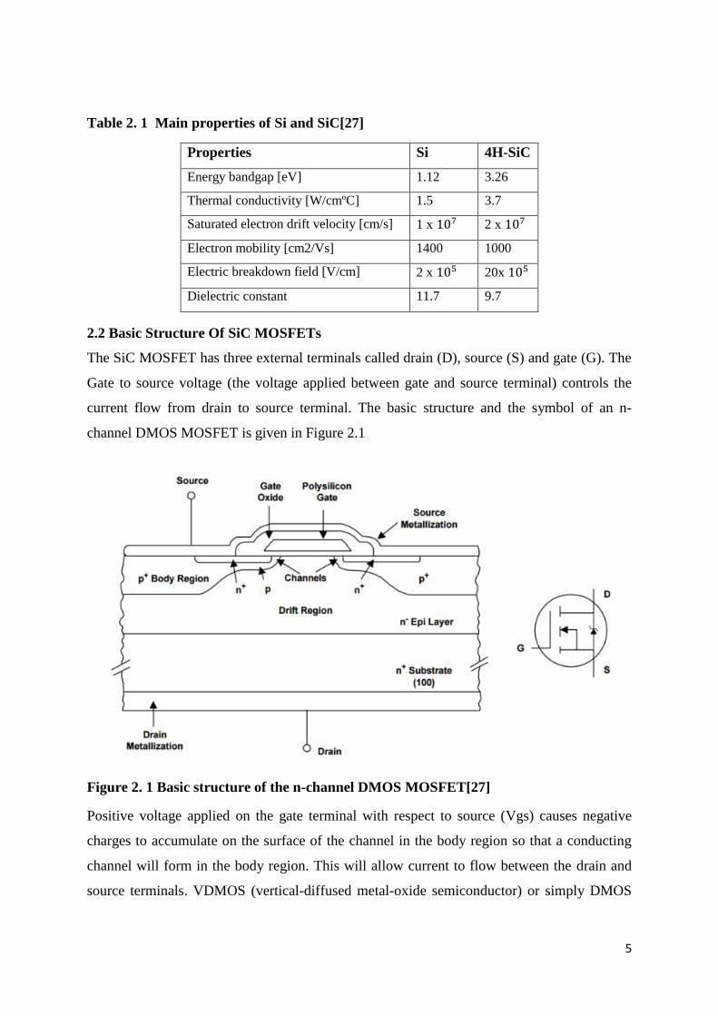
Table 2. 1 Main properties of Si and SiC[27]
Properties Si 4H-SiC
Energy bandgap [eV] 1.12 3.26
Thermal conductivity [W/cmºC] 1.5 3.7
Saturated electron drift velocity [cm/s] 1 x 10⁷ 2 x 10⁷
Electron mobility [cm2/Vs] 1400 1000
Electric breakdown field [V/cm] 2 x 10⁵ 20x 105
Dielectric constant 11.7 9.7
2.2 Basic Structure Of SiC MOSFETs
The SiC MOSFET has three external terminals called drain (D), source (S) and gate (G). The
Gate to source voltage (the voltage applied between gate and source terminal) controls the
current flow from drain to source terminal. The basic structure and the symbol of an n-
channel DMOS MOSFET is given in Figure 2.1
Figure 2. 1 Basic structure of the n-channel DMOS MOSFET[27]
Positive voltage applied on the gate terminal with respect to source (Vgs) causes negative
charges to accumulate on the surface of the channel in the body region so that a conducting
channel will form in the body region. This will allow current to flow between the drain and
source terminals. VDMOS (vertical-diffused metal-oxide semiconductor) or simply DMOS

6
(double-diffused metal-oxide-semiconductor) is the most common power MOSFET structure.
[27]
Figure 2. 2 Power MOSFET structures [27]
However there are also other structures including VMOS and UMOS. The DMOS and
UMOS structures are shown in Figure 2.2
The DMOS structure was the first available Si power MOSFET structure, which was made
available in the 1970s. In the 1990s, the UMOS or Trench MOSFET was introduced in order
to reduce the on-state resistance in the Si power MOSFET. The first available SiC power
MOSFET was introduced in 1994 and had UMOS structure, also called vertical trench
MOSFETs. In the development of SiC MOSFETs in high power applications, the UMOS
structure encountered problems related to increasing the voltage rating. Because of the
trench-positioned gate layer, the peak voltage across the SO2 insulation layer (gate oxide) can
become so high that it causes breakdown of the oxide layer at the trench corners. This
problem was solved by removing the trenches and using the planar DMOS structure, even
though this increases the on-state resistance of the SiC power MOSFET. By this transition
from UMOS to DMOS, the blocking capability of the MOSFET was tripled. The DMOS
structure is the dominating topology in SiC power MOSFETs [27].
2.2.1 SiC MOSFET Parasitic Capacitance
Due to their structure, MOSFETs have a parasitic capacitance, as indicated in Fig.2.3. The
parasitic capacitance highly affects the switching behaviour of a MOSFET and they should
be carefully considered while choosing the operating switching frequency. The drain and
source of a MOSFET are insulated from the gate by the gate oxide film. A PN junction is
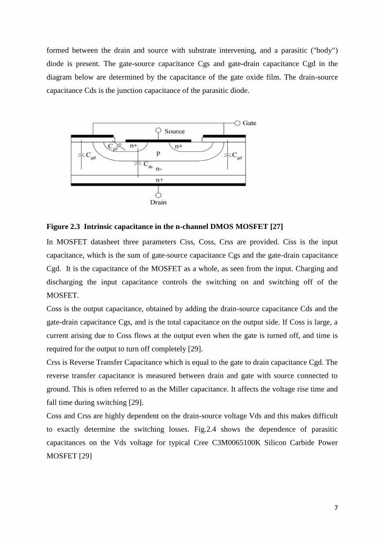
7
formed between the drain and source with substrate intervening, and a parasitic ("body")
diode is present. The gate-source capacitance Cgs and gate-drain capacitance Cgd in the
diagram below are determined by the capacitance of the gate oxide film. The drain-source
capacitance Cds is the junction capacitance of the parasitic diode.
Figure 2.3 Intrinsic capacitance in the n-channel DMOS MOSFET [27]
In MOSFET datasheet three parameters Ciss, Coss, Crss are provided. Ciss is the input
capacitance, which is the sum of gate-source capacitance Cgs and the gate-drain capacitance
Cgd. It is the capacitance of the MOSFET as a whole, as seen from the input. Charging and
discharging the input capacitance controls the switching on and switching off of the
MOSFET.
Coss is the output capacitance, obtained by adding the drain-source capacitance Cds and the
gate-drain capacitance Cgs, and is the total capacitance on the output side. If Coss is large, a
current arising due to Coss flows at the output even when the gate is turned off, and time is
required for the output to turn off completely [29].
Crss is Reverse Transfer Capacitance which is equal to the gate to drain capacitance Cgd. The
reverse transfer capacitance is measured between drain and gate with source connected to
ground. This is often referred to as the Miller capacitance. It affects the voltage rise time and
fall time during switching [29].
Coss and Crss are highly dependent on the drain-source voltage Vds and this makes difficult
to exactly determine the switching losses. Fig.2.4 shows the dependence of parasitic
capacitances on the Vds voltage for typical Cree C3M0065100K Silicon Carbide Power
MOSFET [29]

8
Figure 2.4 Capacitance Vs Drain to Source voltage Vds of Cree C3M0065100K SiC
MOSFET [25]
2.3 Characteristics of SiC MOSFETS
2.3.1 Gate driver voltage Vgs and Rdson
Since SiC has dielectric breakdown field strength 10 times higher than that of Si, high
breakdown voltage devices can be achieved with a thin drift layer with high doping
concentration. This means, at the same breakdown voltage, SiC devices have quite low
specific on-resistance (on-resistance per unit area). Now a days SiC MOSFETs with as low as
16 mili ohm on-resistance are coming to the market [18-20].
Although SiC-MOSFETs have lower drift layer resistance than Si-MOSFETs, the lower
carrier mobility in SiC means their channel resistance is higher. For this reason, the higher
the gate voltage, the lower the on-resistance. The on-resistance of a MOSFET reduces with
increase in gate driver voltages. But once the specified gate driver voltage is reached the on
resistance will saturate and further increasing the gate drive voltage will not decrease the on
resistance. Resistance becomes progressively saturated as Vgs gets higher than 20V. SiC-
MOSFETs do not exhibit low on-resistance with the gate voltage Vgs of 10 to 15V which is
applied to typical IGBTs and Si-MOSFETs. It is recommended to drive SiC-MOFETs with
9
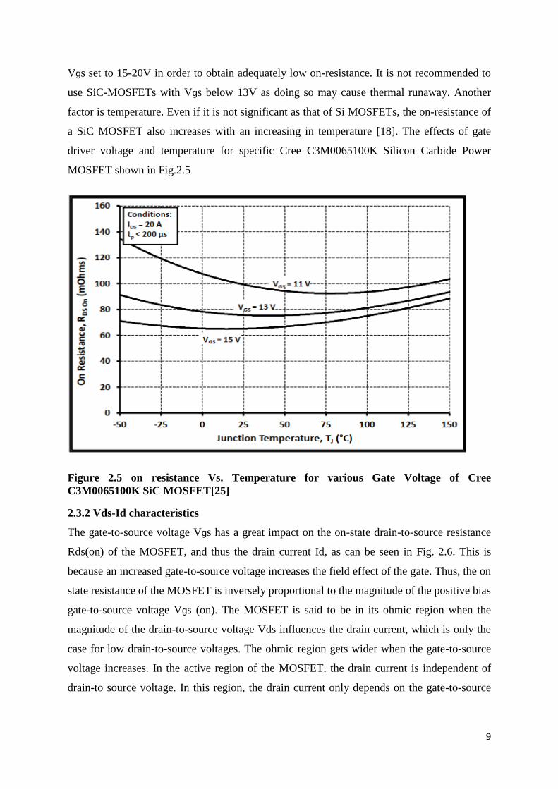
Vgs set to 15-20V in order to obtain adequately low on-resistance. It is not recommended to
use SiC-MOSFETs with Vgs below 13V as doing so may cause thermal runaway. Another
factor is temperature. Even if it is not significant as that of Si MOSFETs, the on-resistance of
a SiC MOSFET also increases with an increasing in temperature [18]. The effects of gate
driver voltage and temperature for specific Cree C3M0065100K Silicon Carbide Power
MOSFET shown in Fig.2.5
Figure 2.5 on resistance Vs. Temperature for various Gate Voltage of Cree
C3M0065100K SiC MOSFET[25]
2.3.2 Vds-Id characteristics
The gate-to-source voltage Vgs has a great impact on the on-state drain-to-source resistance
Rds(on) of the MOSFET, and thus the drain current Id, as can be seen in Fig. 2.6. This is
because an increased gate-to-source voltage increases the field effect of the gate. Thus, the on
state resistance of the MOSFET is inversely proportional to the magnitude of the positive bias
gate-to-source voltage Vgs (on). The MOSFET is said to be in its ohmic region when the
magnitude of the drain-to-source voltage Vds influences the drain current, which is only the
case for low drain-to-source voltages. The ohmic region gets wider when the gate-to-source
voltage increases. In the active region of the MOSFET, the drain current is independent of
drain-to source voltage. In this region, the drain current only depends on the gate-to-source
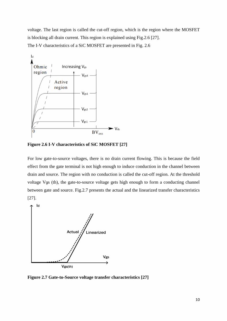
10
voltage. The last region is called the cut-off region, which is the region where the MOSFET
is blocking all drain current. This region is explained using Fig.2.6 [27].
The I-V characteristics of a SiC MOSFET are presented in Fig. 2.6
Figure 2.6 I-V characteristics of SiC MOSFET [27]
For low gate-to-source voltages, there is no drain current flowing. This is because the field
effect from the gate terminal is not high enough to induce conduction in the channel between
drain and source. The region with no conduction is called the cut-off region. At the threshold
voltage Vgs (th), the gate-to-source voltage gets high enough to form a conducting channel
between gate and source. Fig.2.7 presents the actual and the linearized transfer characteristics
[27].
Figure 2.7 Gate-to-Source voltage transfer characteristics [27]
11
2.3.3 SiC MOSFET Switching Characteristics
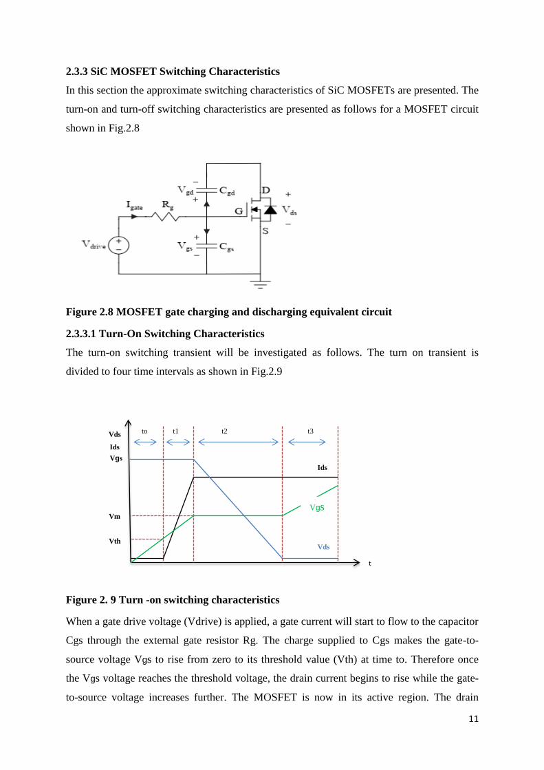
In this section the approximate switching characteristics of SiC MOSFETs are presented. The
turn-on and turn-off switching characteristics are presented as follows for a MOSFET circuit
shown in Fig.2.8
Figure 2.8 MOSFET gate charging and discharging equivalent circuit
2.3.3.1 Turn-On Switching Characteristics
The turn-on switching transient will be investigated as follows. The turn on transient is
divided to four time intervals as shown in Fig.2.9
Figure 2. 9 Turn -on switching characteristics
When a gate drive voltage (Vdrive) is applied, a gate current will start to flow to the capacitor
Cgs through the external gate resistor Rg. The charge supplied to Cgs makes the gate-to-
source voltage Vgs to rise from zero to its threshold value (Vth) at time to. Therefore once
the Vgs voltage reaches the threshold voltage, the drain current begins to rise while the gate-
to-source voltage increases further. The MOSFET is now in its active region. The drain
Vds
Ids
Vgs
Vth
Vm
Vgs
Ids
Vds
to t1 t2 t3
t
12
current will continue to rise along with Vgs (as Rds(on) decreases), until it reaches the
specific current Ids at time t1. At this point, the capacitance Cgs is completely charged and
the gate voltage now remains constant at Miller plateau voltage Vm, while Vds reduces from
Vds;max to switch-on value, Vds;on, during t2. Vds;on is the product of MOSFET on-state
resistance, Rds(on) and Ids. At time t3, the MOSFET enters its ohmic region and the drain-to-
source voltage only depends on the on-state gate resistance. The gate voltage increases
further to gate driver supply level, to fully saturate the MOSFET.
2.3.3.2 Turn-Off Switching Characteristics
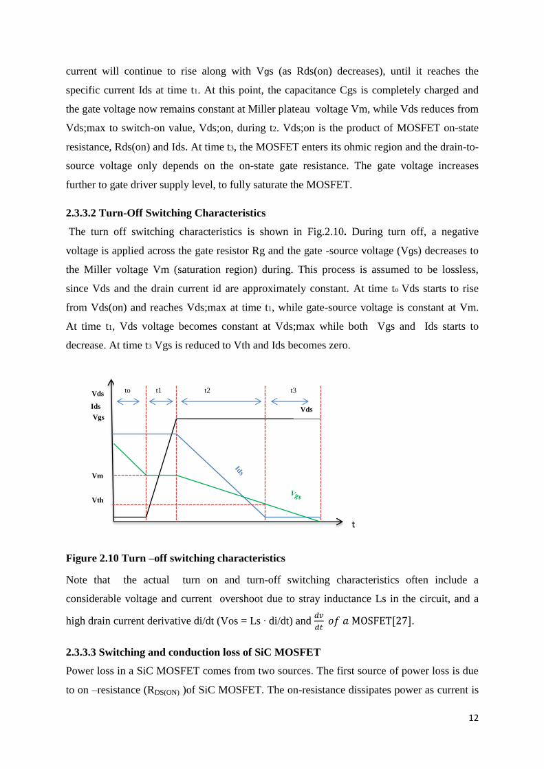
The turn off switching characteristics is shown in Fig.2.10. During turn off, a negative
voltage is applied across the gate resistor Rg and the gate -source voltage (Vgs) decreases to
the Miller voltage Vm (saturation region) during. This process is assumed to be lossless,
since Vds and the drain current id are approximately constant. At time to Vds starts to rise
from Vds(on) and reaches Vds;max at time t1, while gate-source voltage is constant at Vm.
At time t1, Vds voltage becomes constant at Vds;max while both Vgs and Ids starts to
decrease. At time t3 Vgs is reduced to Vth and Ids becomes zero.
Figure 2.10 Turn –off switching characteristics
Note that the actual turn on and turn-off switching characteristics often include a
considerable voltage and current overshoot due to stray inductance Ls in the circuit, and a
high drain current derivative di/dt (Vos = Ls ∙ di/dt) and 𝑑𝑣
𝑑𝑡 𝑜𝑓 𝑎 MOSFET[27].
2.3.3.3 Switching and conduction loss of SiC MOSFET
Power loss in a SiC MOSFET comes from two sources. The first source of power loss is due
to on –resistance (RDS(ON) )of SiC MOSFET. The on-resistance dissipates power as current is
Vds
Ids
Vgs
Vth
Vm
Vds
to t1 t2 t3
t

13
conducted through the device. This kind of loss is called conduction loss. These conduction
losses are inversely proportional to the size of the SiC MOSFET; the larger the switching
transistor, the lower its RDS(ON) and, therefore, its conduction loss.
Conduction losses can be determined as follows
𝑃𝑐 = 𝐼𝑑𝑟𝑚𝑠2 × RDS(ON) (2.1)
Where Pc is conduction loss and 𝐼𝑑𝑟𝑚𝑠 is the rms value of Drain current
The rms value of the drain current can be determined as follows
𝐼𝑑𝑟𝑚𝑠 = √𝐼
𝑇∫ 𝑖𝑠(𝑡)2𝑑𝑡
𝑇
0 (2.2)
The SiC MOSFET conducts for the time of DT , where D is the duty cycle and T is the period
as shown in Fig.3.2 Then the rms current becomes:-
𝐼𝑑𝑟𝑚𝑠 = √𝐼
𝑇𝑠∫ 𝐼𝑠2𝑑𝑡
𝐷𝑇𝑠
0= √
𝐼
𝑇𝑠[𝐼𝑠2 × 𝐷𝑇𝑠] (2.3)
= 𝐼𝑠√𝐷 (2.4)
Figure 2.11 MOSFET current [13]
The other source of power loss is through switching losses. As the MOSFET switches on and
off, it’s intrinsic parasitic capacitance stores and then dissipates energy during each switching
transition. The losses are proportional to the switching frequency and the values of the
parasitic capacitances. As the physical size of the MOSFET increases, its capacitance also
increases; so, increasing MOSFET size also increases switching loss.
And the conduction loss becomes:-
𝑃𝑐 = 𝐼𝑠2 × 𝐷 × RDS(ON) (2.5)

14
These sources of power loss create a significant challenge for power supply designers. While
a larger MOSFET will exhibit less on-resistance and consequently lower conduction loss – its
larger area drives up parasitic capacitance and switching loss. In many cases, moving to a
larger MOSFET to reduce conduction loss will result in so much increased switching loss that
it outweighs the conduction loss savings. Designers typically try to achieve a balance
between conductive and switching losses for a particular application.
The switching loss can be estimated from turn on and turn off energy given in the specific
MOSFET datasheet as follows
Pon=Eon×fs (2.6)
And Poff=Eoff×fs (2.7)
Where Pon/Poff are the turn on/ off Power losses,
Eon /Eoff are the turn on/off energy losses and fs is the switching frequency. The total
switching power loss becomes:-
Psw = Pon + Poff (2.8)
The turn on and turn off energy losses are highly dependent on the gate resistance. Gate
resistor versus turn on /off energy loss graph is provided in the datasheet of a given
MOSFET. Therefor careful manipulation of those graphs is required in order to get
approximate switching power loss. More over the drain current versus energy loss graphs are
also given in the datasheet which is really helpful to determine the exact energy losses
corresponding to the required drain current level.
Figure 2.12 (a) switching energy vs. External gate resistor (b) switching energy vs drain
current[25]

15
Therefor by reading the approximate turn on/off energies for the required drain current and
gate resistors, the total switching loss can be determined by using the Equation 2.8. Carful
determination of power loss is required in order to select appropriate heat sink.
2.4. Bidirectional DC-DC converters
Bidirectional DC-DC converters allow two way power flows as shown in Fig.2.13. Normal
DC-DC converters such as buck and boost converters does not allow the bidirectional power
flow rather power flow is only in one direction. This limitation is due to the presence of the
diode in those converters which allow current flow in one direction only. By replacing those
diodes by controllable power switches like MOSFETs and IGBTs, the unidirectional DC-DC
converters can be changed to Bidirectional DC- DC converters [14-15]
Basically BDCs can be classified into two
1. Non-isolated Bi-directional DC-DC converters (NBDC) and
2. Isolated Bi-directional DC-DC converters (IBDC) types.
Non-isolated BDCs (NBDC) are simpler than isolated BDCs (IBDC) and can achieve better
efficiency. However, galvanic isolation is required in many applications and mandated by
different standards. The complexity of IBDCs stems from the fact that an ac link must be
present in their structure in order to enable power transfer via a transformer [3][16].
2.4.1 Non-isolated BDC
Non-isolated BDC are transformer-less DC-DC converters. They are a derivation of normal
boost type and buck type DC-DC converters by replacing diodes by controllable power
switches. Since they don´t have transformers for isolation purpose, they have better
efficiency, less size, less weight and low cost compared to IBDC. Thus, in the high power or
spacecraft power system applications, where weight or size is the main concern, they are
more preferable [9-12].
Fig.2.13a. shows the structure of NBDC converters and Fig.2.13b. Shows the inductor
waveforms associated with Fig.2.13a. In the buck mode of operation, i.e. when the power is
transferred from the high voltage (HV) to the low voltage (LV) side, Q1 is the active switch
while Q2 is kept off. In the boost mode, i.e. when the power is transferred from LV to HV
side, Q2 acts as a controlled switch and Q1 is kept off. The inductor is the main energy

16
transfer element in this converter. In each switching cycle it is charged through source side
active switch for the duration of :-
Ton=DT (2.9)
Where T=1/fsw is the switching period and D is the duty cycle.
This energy is then discharged to load during Toff= (1-D) T (2.10)
Figure 2.11 (a) Basic NBDC (b) operating waveforms [3]
2.4.2 Isolated BDC (IBDC)
This kind of BDC is preferable when application requires galvanic isolation between multi-
source systems in order to assure personnel safety, noise reduction and correct operation of
protection systems. IBDC have transformer associated with their structure which is used for
isolation and voltage matching purposes since Voltage matching is also needed in many
applications.
The structure of IBDCs is shown in Fig.2.14. It consists of high-frequency switching DC-AC
converters, AC-DC converters and a high-frequency transformer. The transformer is mainly
used for galvanic isolation between two sources and voltage matching. Converter A which is
the DC-AC converter converts the dc source to high frequency ac source or vice versa for the
transformer and converter B converts the output of the transformer to DC power or vice

17
versa. Both converter A and Converter B should be Bidirectional in order to allow the power
flow in both directions [2-4].
Figure 2.12 Basic structure of IBDC [3]
Isolated Bidirectional DC -DC converters can be broadly classified into two categories on the
basis of their configuration:
• A current fed isolated Bidirectional DC-DC converter has an inductor at its terminals which
acts like a current source like a conventional boost converter with an inductor at the input
terminals.
• A voltage fed isolated bidirectional DC-DC converter as shown in the Fig.2.15 has a
capacitor at its terminals which acts like a voltage source like a conventional buck converter
with a capacitor at its input terminals.
Figure 2. 13 Dual Bridge Isolated Voltage Fed Bidirectional DC-DC Converter [3]
Compared to Non-isolated Bidirectional DC -DC converters, the presence of the transformer
in isolated Bidirectional DC-DC converters makes them to be more complex in structure,
more bulky, less efficient, costlier and heavier. Thought this paper the non-isolated half
bridge bidirectional DC-DC converter is used for this project [4-8].

18
2.5 Summary
In this chapter the state of art of SiC MOSFETs and Bidirectional DC-DC converters are
discussed briefly. The important features of SiC materials have been discussed. In addition to
this the main characteristics of SiC MOSFETs are briefly presented in this chapter. Moreover
the Literature review of Bidirectional DC-DC converters is also presented in detail. In chapter
three the design consideration and procedures of Bidirectional DC-DC converters will be
presented in detail.
19
CHAPTER THREE
3. CONVERTER DESIGN METHODOLOGY
3.1 Power Circuit Design Steps
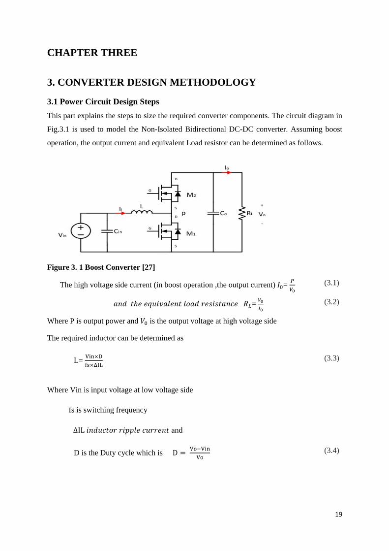
This part explains the steps to size the required converter components. The circuit diagram in
Fig.3.1 is used to model the Non-Isolated Bidirectional DC-DC converter. Assuming boost
operation, the output current and equivalent Load resistor can be determined as follows.
Figure 3. 1 Boost Converter [27]
The high voltage side current (in boost operation ,the output current) 𝐼0= 𝑃
𝑉0 (3.1)
𝑎𝑛𝑑 𝑡ℎ𝑒 𝑒𝑞𝑢𝑖𝑣𝑎𝑙𝑒𝑛𝑡 𝑙𝑜𝑎𝑑 𝑟𝑒𝑠𝑖𝑠𝑡𝑎𝑛𝑐𝑒 𝑅𝐿= 𝑉0
𝐼0 (3.2)
Where P is output power and 𝑉0 is the output voltage at high voltage side
The required inductor can be determined as
L= Vin×D
fs×ΔIL
(3.3)
Where Vin is input voltage at low voltage side
fs is switching frequency
ΔIL 𝑖𝑛𝑑𝑢𝑐𝑡𝑜𝑟 𝑟𝑖𝑝𝑝𝑙𝑒 𝑐𝑢𝑟𝑟𝑒𝑛𝑡 and
D is the Duty cycle which is D = Vo−Vin
Vo (3.4)
20
The inductor ripple current should be appropriately selected and in most application it is
chosen between 20 to 40 percent of the inductor current [13].
The input and output capacitors can be determined as follows [13]
𝐶0 = Iout × D
fs × ΔVo (3.5)
Where ΔVo is the output voltage ripple
Again the input capacitor is also determined as
𝐶𝑖𝑛 = IL × D
fs × Δ𝑉𝑖𝑛 [13] (3.6)
Where ΔV𝑖𝑛 is the input voltage ripple
Ripple voltage is taken between 1-5 % in most power converter designs [13].
Additionally the capacitors should handle the RMS value of inductor ripple current which is
ILrms = ILp−p
2×√3 (3.5)
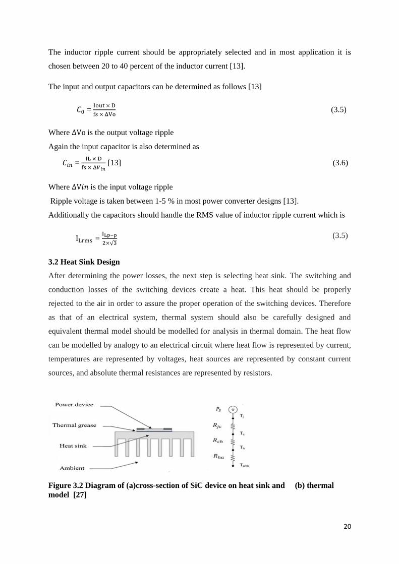
3.2 Heat Sink Design
After determining the power losses, the next step is selecting heat sink. The switching and
conduction losses of the switching devices create a heat. This heat should be properly
rejected to the air in order to assure the proper operation of the switching devices. Therefore
as that of an electrical system, thermal system should also be carefully designed and
equivalent thermal model should be modelled for analysis in thermal domain. The heat flow
can be modelled by analogy to an electrical circuit where heat flow is represented by current,
temperatures are represented by voltages, heat sources are represented by constant current
sources, and absolute thermal resistances are represented by resistors.
Figure 3.2 Diagram of (a)cross-section of SiC device on heat sink and (b) thermal
model [27]

21
The circuit in Fig.3.2a is typical cross-sectional view of a packaged SiC power device
mounted on a heat sink and Fig.3.2b shows the equivalent steady-state thermal circuit.
The junction to case thermal resistance is given in the datasheet of the MOSFETS. From the
equivalent circuit of Fig.3.4b,
Rth Ja = Rjc + Rch + Rha (3.8)
And 𝑇𝑗 − 𝑇𝑎 = Rth Ja × 𝑃𝑙𝑜𝑠𝑠 (3.9)
Where Tj is the device junction temperature and Ta is the ambient temperature
Rjc:- junction to case thermal resistance
Rch :- case to heat sink thermal resistance (it depends on the type of material to be used)
Rha:- heat sink to ambient thermal resistance
The thermal Resistance of the heat sink can be determined as follows:-
Rha = Rth Jc − Rjc + Rch (3.10)
Based on the value of Rh-a appropriate heat sink can be selected.
3.3 Driver circuit design steps and considerations
The turning on and turning off of MOSFET is accomplished by charging and discharging
gate capacitor. Charging the gate capacitor turns the power device on and allows current flow
between its drain and source terminals, while discharging it turns the device off and a large
voltage may then be blocked across the drain and source terminals. The minimum voltage
when the gate capacitor is charged and the device can just about conduct is the threshold
voltage (Vth). For operating an IGBT/power MOSFET as a switch, a voltage sufficiently
larger than Vth should be applied between the gate and source/emitter terminals. SiC
MOSFET requires 15-20V during turn on. However the output of digital controllers or PWM
signals from a microcontroller is not enough to drive power MOSFETs since the voltage is in
a range of 0 to 5V. Thus, an interface is needed between the logic/control circuitry and the
high power device. Gate drivers change voltage levels from microcontroller to the required
gate drive voltage so that the Power MOSFET will be fully on and off [17-20].
The gate driver circuit has three main parts as shown in Fig.3.3. The DC power supply
provides enough sources for the Gate driver IC and Isolation system. Some gate drivers don’t

22
need isolation however it is highly recommended for SiC MOSFET gate drivers. Most
isolation system is separate from the driver IC however now a days there are ICs with internal
isolation system which will save space and time [22][28].
Figure 3.3 Components of gate driver circuit
The following features are required for SiC MOSFET Gate drivers
3.3.1 Wide range of Gate voltages
The gate driver IC has to fulfil the range of positive and the negative gate voltage for
optimized operation of the SiC MOSFET. The positive gate-source voltage defines the on-
state RDS(on) of the SiC MOSFET. Increasing Positive gate voltage will result in reduction
of RDS(on) resistance which in turn results low conduction losses. Currently most SiC
MOSFETs available in the market requires in a range of 15-25V positive gate voltage in
order to perform efficiently. A lower gate voltage level is of course possible, but it results in
an increase of the steady-state channel resistivity and therefore higher conduction losses.
Table 3.1 shows the different gate-source voltage requirements and limits of currently
available SiC MOSFETs.
In addition to the positive gate voltage requirements, the gate driver should also provide the
required negative voltage for turning off the MOSFET properly. The minimum gate-source
threshold voltage Vgs(th) of SiC MOSFET devices can be lower than 2 Vat 25°C in some
cases. Therefore, minor ground bouncing can lead to an uncontrolled turn-on of the MOSFET
when using an off-state voltage of zero Volts. This situation could get more critical if one
takes the temperature drift of the gate-source voltage threshold into account. A negative turn-
off gate voltage can relax the situation and keeps the MOSFET in off-state even in noisy
environments. On the other hand, it is known that too low negative gate voltages can limit the
lifetime of such MOSFETs. The level of the negative gate voltage depends on the gate-source

23
threshold voltage as well as on the required gate charge for turning on the MOSFET. Thus,
the driver ICs for SiC MOSFET should have the capability of managing a small negative gate
voltage in order to provide a safe and stable off-state condition of SiC MOSFET [17][18].
3.3.2 Output current Requirement
The gate driver should source the peak current requirements of the gate of the power
MOSFET and it must be high enough to drive the lowest chosen gate resistor value with the
highest chosen gate voltage swing. The peak current requirement can be calculated as follows
Ip =∆𝑉𝐺
𝑅𝐺𝑒𝑥𝑡+𝑅𝑖𝑛𝑡 (3.11)
Where ∆𝑉𝐺 Is the difference between the positive and negative gate source voltage RGext
and Rint are the required external and internal gate resister respectively.
3.3.3 Input-Output Delay Time
There is a small delay between input and output of the gate driver IC. This delay varies with
temperature and should be as low as possible. However the significance of this propagation
delay for dead time calculations is less compared to the turn on and turn of delays of power
MOSFET.
Table 3. 1 Gate to source voltage limits for different SiC MOSFET
VGS Voltage(V) JFET cascode MOSFET 2nd gen MOSFET 3rd gen
25
20
Maximum Limit
Recommended Range
15
10
5
0
-1
-2
-3
-4
-5
-10
-15
-20
-25
24
3.3.4 Other considerations
In addition to the points mentioned above the gate driver should also operate at different
temperature ranges. The maximum junction temperatures of most available Driver IC’s are
150oC which enables the gate driver to work at harsh environment. In addition to this the
gate driver IC should have also high level of insulation voltage which is usually
recommended above 2500vrms for high power switching device applications. Moreover the
Driver IC is also required to have under voltage lock out, short circuit protection and over
voltage protection features which guarantee for safety operation [22-24].
3.4 Control system design
Closed-loop feedback system is implemented in most switching power supplies to provide
stable power under various transient and load conditions. There are two types of feedback
methodology,
1. Voltage mode control (VMC) and
2. Current mode control (CMC).
3.4.1 Voltage mode control (VMC)
This methodology provides simple, straight–forward feedback architecture for the control
path. A scaled value of the output voltage is used as the feedback signal. However the output
voltage regulation requires sensing a change in output voltage and propagation through the
entire feedback signal and filter before the output is appropriately compensated. This can
generate unacceptably slow response for systems that desire high levels of regulation. The
feedback compensation of the supply requires a higher level of analysis to address the two
poles introduced by the output low–pass filter. Additionally, the feedback component values
must be adjusted since different input voltages affect the overall loop gain [21].
3.4.2 Current mode control (CMC)
Current mode control addresses the above short-falls of voltage mode control by using the
inductor current waveform for control. This signal is included with the output voltage
feedback loop as a second, fast response control loop. While current mode control addresses
some of the drawbacks of VMC, it introduces challenges that can affect the circuit
performance. The addition of the current feedback loop increases the complexity of the
control/feedback circuit and circuit analysis. Stability across the entire range of duty cycles

25
and sensitivity to noise signals are other items that need to be considered in the selection of
current mode control [21][30].
The two most common methodologies used in circuit design are peak and average current
mode control.
3.4.2.1 Peak Current Mode Control
Peak current mode control (PCMC) utilizes the current waveform directly as the ramp
waveform into the PWM–generation comparator instead of an externally generated sawtooth–
or triangle–signal like VMC. The upslope portion of the inductor current or high–side
transistor current waveform is used to provide a fast response control loop in addition to the
existing voltage control loop. As shown in Fig 3.4(a), the current signal is compared with the
output of the voltage error amplifier to generate the PWM control signal for the power supply
[21].
Figure 3.4(a) Peak current control scheme (b) average current control scheme [21]
Peak current control mode have poor noise immunity ,need slop compensation and has Peak
to average current error. Moreover the peak current control only controls inductor current and
it is mostly effective only in controlling the output current of buck converter since the
inductor is in the output side in buck converter. However it cannot be used in boost converter
output current control [21].

26
3.4.2.2 Average Current Mode Control
Average current mode control (ACMC) utilizes the inductor current waveform and an
additional gain and integration stage before the signal is compared to an externally provided
ramp waveform (similar to VMC). This allows improved immunity to noise and removes the
need for slope compensation. Fig.3.4(b) shows a block diagram of ACMC operation for a
buck converter. In this project the Average Current Mode Control method is used and the
details of the design procedures can be referred in [30].
3.4.3 MOSFET Dead Time
In a system which has a Complementary PWM signals dead time is required in order to
protect cross conduction. When one MOSFET is on the other MOSFET should be kept off .if
the two complementary switching devices are on at the same time there will be a short circuit
from power to ground which causes large current spikes even for short a duration causes. The
current spike increases thermal output of switching devices which causes wears out of the
switching devices and blow up the whole circuit. Therefor dead time should be provided so
that the two complementary switching devices will not be on at the same time the dead time
and ensures that one switching device has fully turned off before the other complementary
switching device starts to turn on. The grey area between one signal turning off and the other
one turning on, shown in Fig.3.5 is the dead time.
Figure 3.5 Dead time added on the complementary PWM signals [21]
Even if adding dead time has an advantage of protecting large surge currents and short
circuit, it has also a disadvantage. The more dead time added the less efficient the converter
will be, since during that period it's not actually doing anything at all. But, if the dead time is
too short the converter will suffer short circuit and heating. Therefore proper dead time
should be tunned by considering the characteristics of the switching devices (MOSFET or
IGBT, for instance).

27
There are so many options to put dead time in the DC-DC converter. The dead time can be
added by using Digital controllers like DSP or it can be implemented by using Schemitt
trigger IC and RC circuits. The simple dead time circuit is shown in Fig.3.6 by using
Schemitt trigger IC and RC circuits.
Figure 3. 6 Dead time circuit using Schemitt trigger and RC components [29]
3.5 PCB design considerations
It is expected that every switching power supply should provide clear and stable power to the
loads. Unfortunately, this does not always happen. A common problem of switching power
supplies is unstable switching waveforms. If the problem is related to the printed circuit
board (PCB) layout, identifying the cause can be difficult and it is always necessary to
prepare proper PCB layout at the early stage of a switching supply design. A good layout
design optimizes supply efficiency, alleviates thermal stress, and most importantly,
minimizes the noise and interactions among traces and components [31].
In designing PCB the length of conduction path should be minimized as much as possible. If
the board has embedded DC-DC supplies, the supply output should be located close to the
load devices in order to minimize the interconnection impedance and the conduction voltage
drop across the PCB traces to achieve best voltage regulation, load transient response and
system efficiency. In designing power stage of a converter careful attention should be given
to the current traces. The large current traces should be short and wide to minimize PCB
inductance, resistance and voltage drop. This is especially critical for the traces with high
di/dt pulsating current flow.
On a multilayer PCB board, it is highly desirable to place the DC ground or DC input or
output voltage layers between the high current power component layer and the sensitive small
signal trace layer. The ground and/or DC voltage layers provide AC grounds to shield the
small signal traces from noisy power traces and power components. As a general rule, the

28
ground or DC voltage planes of a multilayer PCB should not be segmented. If the
segmentation is unavoidable, the number and length of traces in these planes must be
minimized. The traces should also be routed in the same direction as the high current flow
direction to minimize the impact [27][31].
PCBs can be designed using computer software, e.g. CadSoft Eagle and Altium. The
component package footprints should be carefully designed and drawn in order not to face
problems during mounting of components. It is also necessary to choose appropriate
clearance and creepage. If necessary, using Vias can also reduce complexity making
soldering easier [27].
When a PCB design is ready for manufacturing, it can be manufactured through different
methods. Popular solutions are etching and milling. PCB milling often gives the most
accurate result for small and detailed PCBs [27].

29
CHAPTER FOUR
4. CASE –STUDY
In this part the details of the Design of 20KW Bidirectional DC-DC converter is presented.
The DC-DC converter should have less weight and less loss as much as possible and have
targeted efficiency of above 98%. Proper switching frequency should also be selected by
considering the Switching losses of the MOSFETs and the required size of the inductor. The
high voltage side or the dc link voltage is required to be 800V and the low voltage side is
400V. In addition to this proper control system should be implemented in order to control the
inductor current. In most of the converter designs here at Zigor Corporation, the inductor
current ripple is taken as 33% of the average inductor current and the voltage ripple is 1%.
Therefor in this thesis work the same amount of current and voltage ripple is considered.
4.1 Power circuit Design
4.1.1 Choosing SiC MOSFETs
SiC MOSFETs from three different manufacturers (Wolfspeed, United Silicon Carbide and
Infineon) are compared based on the switching losses and their on resistance. However SiC
MOSFETs from Infineon are desired for large current and power applications and in this
thesis work we considered only SiC MOSFETs from the other two manufacturers.
The turn on and turn off energy losses and on resistances of the MOSFETs are taken from
their datasheet. The switching and conduction losses are determined based on Equation.2.5-
2.8. Moreover connecting two MOSFETs in parallel has also an advantage of reducing
switching and conduction losses since the current is divided in to two of the MOSFETs and
the conduction loss is proportional to the square of the drain current. Taking account of the
minimum RD on resistance, second generation C2M0040120D and third generation
C3M003090K Cree MOSFETs from Wolfspeed and UF3C120040K4S from United Silicon
Carbide's Cascode products, are considered in this project. The result is summarized on Table
4.1. Based on the results in Table 4.1 third generation Cree MOSFET (C3M003090K) has
less switching losses compared to 2nd
generation Cree MOSFET (C2M0040120D) and United
Silicon carbide MOSFETs. However, C3M003090K and UF3C120040K4S MOSFETs are
selected for this project and the DC-DC converter is designed in order to work for both
MOSFETs.

30
Table 4. 1 Comparison of switching energy loses for Different SiC MOSFETs
4.1.2. Selecting Switching frequency, the required inductor, Capacitors and Heat sink
Minimizing inductor size and switching loss are our design constraint. Both are dependent on
the switching frequency. As discussed in chapter 3 the size of the inductor is inversely
proportional to the switching frequency. To make rough estimation, firstly the size of the
required inductor is compared with the respective switching frequency according to Equation
3.3 and the result is summarized in Table 4.2. As it can be seen clearly higher switching
frequencies decrease the required size of inductor significantly.
Table 4. 2 Size of inductor for various frequencies
Switching
Frequency(KHz)
Inductor
Size(uH)
20 606
25 484
30 404
35 346
40 303
However higher switching frequencies will lead to noise and higher switching losses as
summarized on Table 4.1 which in turn requires larger Heat sink. Therefor by taking in to
account of the required inductor size, switching losses and available cores to make the
inductors here at Zigor Corporation, 35KHz switching frequency is selected for our design.
After choosing the switching frequency, the next step is sizing inductor, capacitors and
selecting the heat sink. The mathematical details of Bidirectional DC-DC converter are
W
olfs
peed
Fsw Eon Eoff Pon Poff Switchingloss Pconduction Ploss total
20000 1.40E-03 3.00E-04 2.80E+01 6.00E+00 6.80E+01 6.25E+01 1.31E+02
25000 1.40E-03 3.00E-04 3.50E+01 7.50E+00 8.50E+01 6.25E+01 1.48E+02
30000 1.40E-03 3.00E-04 4.20E+01 9.00E+00 1.02E+02 6.25E+01 1.65E+02
35000 1.40E-03 3.00E-04 4.90E+01 1.05E+01 1.19E+02 6.25E+01 1.82E+02
20000 6.00E-04 2.50E-04 1.20E+01 5.00E+00 6.80E+01 15.625 8.36E+01
25000 6.00E-04 2.50E-04 1.50E+01 6.25E+00 8.50E+01 15.625 1.01E+02
30000 6.00E-04 2.50E-04 1.80E+01 7.50E+00 1.02E+02 15.625 1.18E+02
35000 6.00E-04 2.50E-04 2.10E+01 8.75E+00 1.19E+02 15.625 1.35E+02
20000 4.10E-04 8.20E-05 8.20E+00 1.64E+00 3.94E+01 18.75 5.81E+01
25000 4.10E-04 8.20E-05 1.03E+01 2.05E+00 4.92E+01 18.75 6.80E+01
30000 4.10E-04 8.20E-05 1.23E+01 2.46E+00 5.90E+01 18.75 7.78E+01
35000 4.10E-04 8.20E-05 1.44E+01 2.87E+00 6.89E+01 18.75 8.76E+01
20000 9.00E-04 3.00E-04 1.80E+01 6.00E+00 9.60E+01 87.5 1.84E+02
25000 9.00E-04 3.00E-04 2.25E+01 7.50E+00 1.20E+02 87.5 2.08E+02
30000 9.00E-04 3.00E-04 2.70E+01 9.00E+00 1.44E+02 87.5 2.32E+02
35000 9.00E-04 3.00E-04 3.15E+01 1.05E+01 1.68E+02 87.5 2.56E+02
20000 6.00E-04 1.50E-04 1.20E+01 3.00E+00 6.00E+01 21.875 8.19E+01
25000 6.00E-04 1.50E-04 1.50E+01 3.75E+00 7.50E+01 21.875 9.69E+01
30000 1.69E-03 3.50E-04 5.07E+01 1.05E+01 1.22E+02 21.875 1.44E+02
35000 1.68E-03 3.50E-04 5.88E+01 1.23E+01 1.42E+02 21.875 1.64E+02
Cre
e M
osf
ets
from
wolf
spee
d
UF3
C1
20
04
0K
4S
Un
ited
Sil
ico
n C
arb
ide
Sin
gle
Par
alle
l
C2
M0
04
01
20
D Sin
gle
Par
alle
l
C3
M0
03
09
0K
Par
alle
l

31
discussed in chapter three. All the calculations are made for boost operation (since the
parameters can be used for buck operation). Therefore the output current and equivalent Load
resistor can be determined as follows in Boost operation
𝐼0 = 𝑃
𝑉0 =
20,000
800 =25A (4.1)
𝑅𝐿= 𝑉0
𝐼0 =
800
25 = 32ꭥ (4.2)
The average inductor current is 50A. The Duty cycle is 0.5 and considering 33% inductor
current ripple, the required inductor is sized as
L= Vin×D
fs×ΔIL (4.3)
= 400×0.5
35,000×0.33×50 = 346µH (4.4)
The required inductor is designed in our workshop using K8020E040 E shape magnetic core
as shown below.
Again considering 1% output voltage ripple, the required output capacitor is sized as follows
𝐶0 = Iout×D
fs×ΔVo (4.5)
= 25×0.5
35,000×0.01×800 = 44.6µF (4.6)
In this design two Metallized Polypropylene Film capacitors to be connected in parallel each
with 25A ripple current and 25uF capacitance is selected from KEMET.
Again the input capacitor is also determined as
𝐶𝑖𝑛 = IL×D
fs×Δ𝑉𝑖𝑛 (4.7)
Figure 4. 1 Designed inductor
32
= 50×0.5
35,000×0.01×400 =180µF (4.8)
The RMS value of inductor ripple current is
ILrms = ILp−p
2×√3 (4.9)
= 0.33×50
2×√3 = 4.61A (4.10)
Therefore four Aluminium Electrolytic capacitors (two in series and two in parallel) each
with 220uF is selected from KEMET.
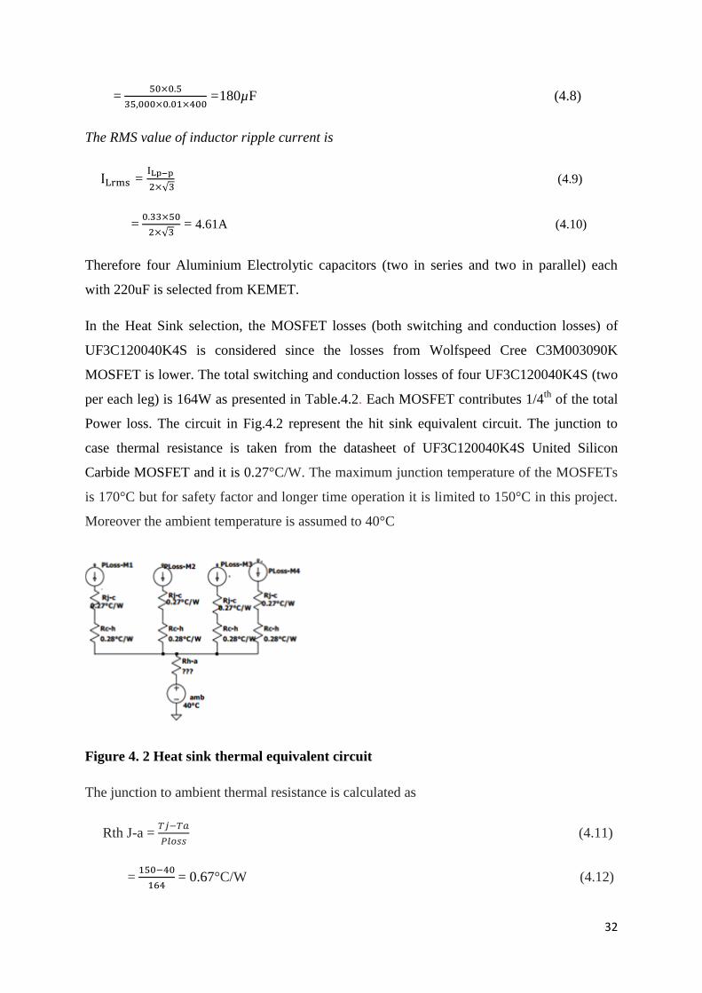
In the Heat Sink selection, the MOSFET losses (both switching and conduction losses) of
UF3C120040K4S is considered since the losses from Wolfspeed Cree C3M003090K
MOSFET is lower. The total switching and conduction losses of four UF3C120040K4S (two
per each leg) is 164W as presented in Table.4.2. Each MOSFET contributes 1/4th
of the total
Power loss. The circuit in Fig.4.2 represent the hit sink equivalent circuit. The junction to
case thermal resistance is taken from the datasheet of UF3C120040K4S United Silicon
Carbide MOSFET and it is 0.27°C/W. The maximum junction temperature of the MOSFETs
is 170°C but for safety factor and longer time operation it is limited to 150°C in this project.
Moreover the ambient temperature is assumed to 40°C
Figure 4. 2 Heat sink thermal equivalent circuit
The junction to ambient thermal resistance is calculated as
Rth J-a = 𝑇𝑗−𝑇𝑎
𝑃𝑙𝑜𝑠𝑠 (4.11)
= 150−40
164 = 0.67°C/W (4.12)
33
To determine the thermal resistance of the heat sink, the parallel combinations of the circuit
at Fig 4.2 should be solved
Hence, Rth J-a = Rj-c + Rc-h+ Rh-a (4.13)
Rj-c+Rc-h = 1/4× (0.27+0.28) °C/W = 0.1375°C/W (4.14)
Therefore the thermal resistance of the required heat sink becomes
Rh-a = Rth J-c - Rj-c+Rc-h (4.15)
= 0.67°C/W- 0.1375°C/W=0.5°C/W (4.16)
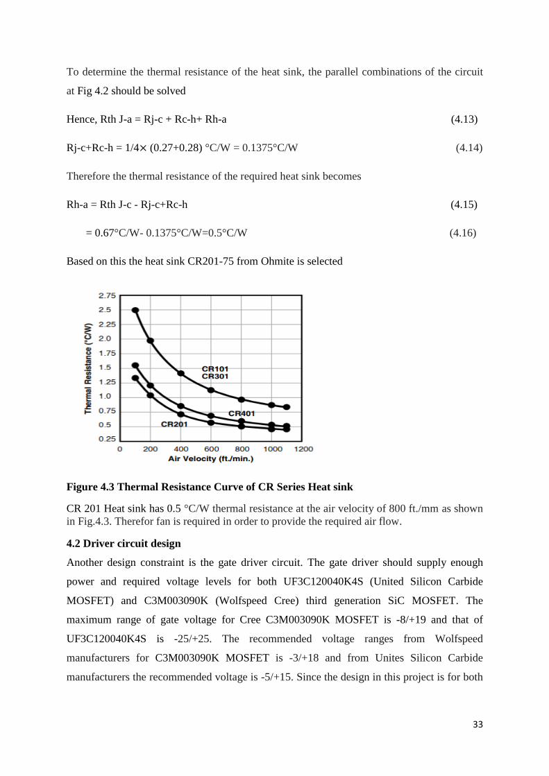
Based on this the heat sink CR201-75 from Ohmite is selected
Figure 4.3 Thermal Resistance Curve of CR Series Heat sink
CR 201 Heat sink has 0.5 °C/W thermal resistance at the air velocity of 800 ft./mm as shown
in Fig.4.3. Therefor fan is required in order to provide the required air flow.
4.2 Driver circuit design
Another design constraint is the gate driver circuit. The gate driver should supply enough
power and required voltage levels for both UF3C120040K4S (United Silicon Carbide
MOSFET) and C3M003090K (Wolfspeed Cree) third generation SiC MOSFET. The
maximum range of gate voltage for Cree C3M003090K MOSFET is -8/+19 and that of
UF3C120040K4S is -25/+25. The recommended voltage ranges from Wolfspeed
manufacturers for C3M003090K MOSFET is -3/+18 and from Unites Silicon Carbide
manufacturers the recommended voltage is -5/+15. Since the design in this project is for both

34
Wolfspeed and Unites Silicon Carbide MOSFETs, a voltage range of -3/+15 is selected.
Therefore the gate driver should supply +15 volt for turn on and -3V for turning off.
Again the manufacturers from Wolfspeed recommend to use 3-5ꭥ external gate resistor and
United Silicon Carbide manufacturers recommend to use 10ꭥ external gate resistor. The peak
current required for both types of SiC MOSFETs determined as follows
For C3M003090K Wolfspeed MOSFET, the internal gate resistance is 3ꭥ and the peak
current is Ipeak = Δ𝑉𝐺𝑠
𝑅𝐺𝑖𝑛𝑡+𝑅𝐺𝑒𝑥 (4.17)
= +15−(−3)
3+3 = 3.12A (4.18)
Again for UF3C120040K4S Unites Silicon Carbide MOSFETs, the internal gate resistance is
4.5ꭥ. The peak current is
Ipeak = Δ𝑉𝐺𝑠
𝑅𝐺𝑖𝑛𝑡+𝑅𝐺𝑒𝑥 =
+15−(−3)
4.5+10 = 1.31A (4.19)
Since the peak current required by UF3C120040K4S is lower than C3M003090K MOSFETs,
the gate driver is designed based on the C3M003090K MOSFETs. Moreover the gate driver
should be capable of supplying two MOSFETs in parallel and the peak current rating of the
gate driver should be greater than 2× 3.12A.
Based on this SIC1182K gate driver from Power integrations is selected. It is a single channel
gate driver and has a capacity of supplying ±8A peak output current. Moreover it has
reinforced galvanic isolation and important features like advanced active clamping (at turn-
off phase), short-circuit protection, overvoltage protection, under voltage lock-out (UVLO).
Therefore for this project two SIC1182K gate driver IC’s (one per each leg) are selected.
In addition to this DC power supply for gate driver circuit is selected. The turn on and turn
off energy requirements of the gate is
Eon = Eoff = 1/2× Cgs×𝑉𝑔𝑠2 (4.20)
Where Cgs is the gate-to- source capacitance and Vgs is the applied drive voltage
The total energy dissipation becomes

35
Et= Eon+Eoff=Cgs×𝑉𝑔𝑠2 (4.21)
And the Power dissipation becomes
P=Et×Fsw = Cgs×𝑉𝑔𝑠2 × Fsw (4.22)
Approximately the power dissipation can be determined as
P=Qg× Vgs×Fsw (4.23)
Therefor by taking the datasheet values of Qg as 87nC
P = 87nC×18V×35000Hz = 0.05WDC power supply having a capacity of 2W from RECOM
is selected. Moreover the input voltage of the Driver IC should be +15/-3V in order to get the
required gate driver voltage. Therefore the selected DC power supply has output voltage of
+15/-3V. For each gate driver IC, one DC power supply is selected. Small inductors and
capacitors are used in each power supply in order to filter out the high frequency components.
The schematic diagram of the power stage circuit and driver circuit of the Bidirectional DC-
DC converter is shown in Fig.4.5.
4.3. Control circuit design
As mentioned before the control circuit is based on average current control method. The
details of the calculations and formulas are found in [31]. The formulas and details of the
calculation can be referred there. The control loop is designed for buck operation to control
the inductor current (output current).
4.3.1 Current loop design
Sawtooth slope;
𝑑𝑉𝑠
𝑑𝑡 =
𝑉𝑠
𝑇𝑠 (4.24)
Where Vs is the amplitude of the Sawtooth voltage and Ts is period. Therefor
𝑑𝑉𝑠
𝑑𝑡 = 4V/1/35KHZ = 0.14V/µsec (4.25)
To sense the inductor current CQ-2335, High-Speed Small Current Sensor is selected. Hence
from the datasheet of the selected current sensor sensitivity is taken which is:

36
𝑑𝑉𝑖
𝑑𝐼 = 25mV/A (4.26)
the rate of change of inductor current is 𝑑𝐼𝐿
𝑑𝑡 = Vo/L = 400/350µH = 1.142A/ µsec (4.27)
𝑑𝑉𝑖
𝑑𝑡 =
𝑑𝑉𝑖
𝑑𝐼𝐿×
𝑑𝐼𝐿
𝑑𝑡 = 25mV/A×1.142A/ µsec = 0.0285V/µsec (4.28)
The current amplifier gain is
GCAmax = Vi
VCA =
𝑑𝑉𝑠
𝑑𝑡𝑑𝑉𝑖
𝑑𝑡
⁄ = 0.14v/0.0285 = 4.5 (4.29)
Back off some percent to allow additional down slop and take 4 as GCA
𝑅𝑓𝑖
𝑅𝑖𝑖 = GCA= 2 (4.30)
Then the following resistance values are chosen Rii=5K and Rfi=20K
The cross over frequency is:
Fc = fs
2𝜋D (4.31)
= 35000
2×3.14×0.5 =11.14Khz (4.32)
Civ = 1
2𝜋×𝑓𝑐
2×𝑅𝑓𝑖
= 1.428nF (4.33)
4.3.2 Voltage loop Design
Inductor current downslope (during OFF time), converted into an equivalent voltage
downslope by Rc, the output capacitor ESR
𝑑𝐼𝐿
𝑑𝑡 =Vo/L=400/350µH = 1.142A/ µsec (4.34)
𝑑𝑉𝑣
𝑑𝑡 = ESR×
𝑑𝐼𝐿
𝑑𝑡= 2.8𝑚ꭥ×1.142A / µsec=3.2mV/ µsec (4.35)
Because of slope limitations at the PWM comparator, the Sawtooth slope at the VA output
must be limited to 1/2 the slope across dvi/dt [31].
Thus the voltage amplifier gain at fs is
GVAmax = VvA
Vi =
𝑑𝑉𝑖
𝑑𝑡
2𝑑𝑉𝑣
𝑑𝑡
⁄ =28.5Mv
2×3.2mV= 4.5 (4.36)

37
Taking GVA to 4 gives Rfv = 4K and Rfi = 1k
Cfv = Civ = 1(2𝜋 × 𝑓𝑐 × 𝑅𝑓𝑣)⁄ = 3.5nF (4.37)
4.3.3 Dead time circuit
In order to protect cross conduction, dead time circuit is designed as shown in Fig.4.3. The
dead time circuit is connected to the average current controller PWM signal. 74HC240
inverting octal buffer IC and RC circuit is used in order to add the dead time. Moreover
NAND gate is used in order to enable and disable the octal buffer so that the high and low leg
PWM signals can be controlled (turned on/off) using the toggle switch.
Figure 4. 4 Schematic circuit used to generate Dead time
4.4. PCB design
In this project a total of two PCB is required. One PCB is for power stage and driver circuit.
The other PCB is for control system. However due to time and material limitation the PCB is
designed only for power stage and driver circuit. The control system is designed by using
breadboards. The PCB having two layers (Top and bottom layers) is designed using
CADSTAR software. Gate drivers are made closer to the MOSFETs. Moreover the DC
power supply for the gate drivers are close enough to the Gate driver IC in order to minimize
the interconnection impedance and the conduction voltage drop across the PCB traces to
achieve best voltage regulation . Most of the components are placed on the Top layer. Only
the heat sink and the SiC MOSFETs are placed on the bottom layer. Careful attention is given
to the length of the traces in order to minimize voltage drop. Rule of thumb is used to
determine the size of the traces which is 1mm per Ampere. In addition to this short and wide
traces are used for the power stage to minimize PCB inductance, resistance and voltage drop.

38
Careful attention was given for the clearance of the traces. The Top and bottom PCB design
is shown in Fig.4.7 and Fig 4.8. Finally the components are placed as shown in Fig.4.9.
4.5 Double pulse test Set Up
Double pulse test is used to study and analyse the switching behaviour of switching devices.
This test helps to determine the switching power losses of SiC MOSFETs. In half bridge
MOSFETs, one MOSFET is replaced with a diode and double pulse is applied to the other
MOSFETs as shown in Fig.4.5a.
Generally the double pulse is designed in order to supply pulses with different on time as
shown in Fig.4.5b
At the instant t1 the DUT is turned on and the inductor is charged up to the desired current
level. The time t1 should be enough to set up the inductor current at required level according
to the following formulas
At time t1, the inductor voltage VL= VDC = L𝑑𝐼𝐿
𝑑𝑡 (4.38)
From this Δt1 = L × IL/VDC (4.39)
Where L is load inductance and IL is an inductor current
t2 and t3 can be chosen each to half of the period or 1/switching frequency
Figure 4. 5 (a) Double pulse test circuit (b) wave form of applied pulse ,transistor
current and inductor current
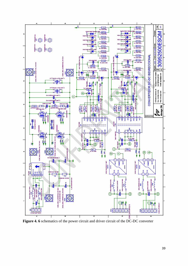
39
Figure 4. 6 schematics of the power circuit and driver circuit of the DC-DC converter
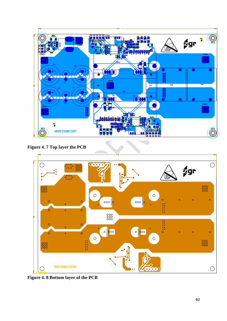
40
Figure 4. 7 Top layer the PCB
Figure 4. 8 Bottom layer of the PCB
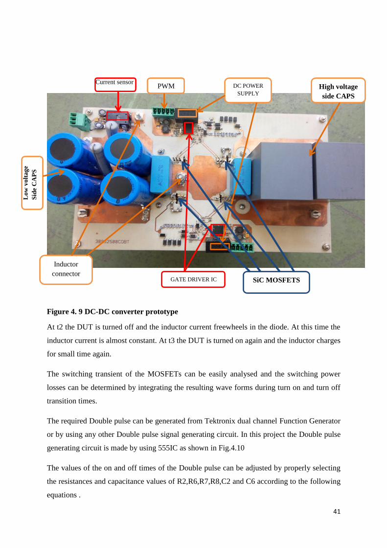
41
Current sensor
GATE DRIVER IC
Figure 4. 9 DC-DC converter prototype
At t2 the DUT is turned off and the inductor current freewheels in the diode. At this time the
inductor current is almost constant. At t3 the DUT is turned on again and the inductor charges
for small time again.
The switching transient of the MOSFETs can be easily analysed and the switching power
losses can be determined by integrating the resulting wave forms during turn on and turn off
transition times.
The required Double pulse can be generated from Tektronix dual channel Function Generator
or by using any other Double pulse signal generating circuit. In this project the Double pulse
generating circuit is made by using 555IC as shown in Fig.4.10
The values of the on and off times of the Double pulse can be adjusted by properly selecting
the resistances and capacitance values of R2,R6,R7,R8,C2 and C6 according to the following
equations .
DC POWER
SUPPLY
PWM
Lo
w v
olt
ag
e
Sid
e C
AP
S
High voltage
side CAPS
Inductor
connector SiC MOSFETS
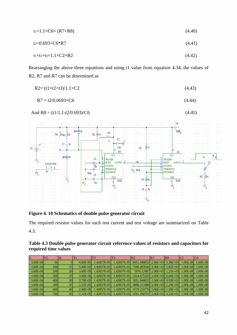
42
t1=1.1×C6× (R7+R8) (4.40)
t2=0.693×C6*R7 (4.41)
t1+t2+t3=1.1×C2×R2 (4.42)
Rearranging the above three equations and using t1 value from equation 4.34, the values of
R2, R7 and R7 can be determined as
R2= (t1+t2+t3)/1.1×C2 (4.43)
R7 = t2/0.0693×C6 (4.44)
And R8 = (t1/1.1-t2/0.693)/C6 (4.45)
Figure 4. 10 Schematics of double pulse generator circuit
The required resistor values for each test current and test voltage are summarized on Table
4.3.
Table 4.3 Double pulse generator circuit reference values of resistors and capacitors for
required time values
L VL IL T1 T2 T3 R2 R7 R8 C2 C6
3.60E-04 30 5 6.00E-05 1.42857E-05 1.42857E-05 8051.948052 2.06E+03 3.39E+03 1.00E-08 1.00E-08
3.60E-04 100 15 5.40E-05 1.42857E-05 1.42857E-05 7506.493506 2.06E+03 2.85E+03 1.00E-08 1.00E-08
3.60E-04 200 20 3.60E-05 1.42857E-05 1.42857E-05 5870.12987 2.06E+03 1.21E+03 1.00E-08 1.00E-08
3.60E-04 300 25 3.00E-05 1.42857E-05 1.42857E-05 5324.675325 2.06E+03 6.66E+02 1.00E-08 1.00E-08
3.60E-04 400 30 2.70E-05 1.42857E-05 1.42857E-05 5051.948052 2.06E+03 3.93E+02 1.00E-08 1.00E-08
3.60E-04 500 35 2.52E-05 1.42857E-05 1.42857E-05 4888.311688 2.06E+03 2.29E+02 1.00E-08 1.00E-08
3.60E-04 600 40 2.40E-05 1.42857E-05 1.42857E-05 4779.220779 2.06E+03 1.20E+02 1.00E-08 1.00E-08
3.60E-04 700 45 2.31E-05 1.42857E-05 1.42857E-05 4701.298701 2.06E+03 4.25E+01 1.00E-08 1.00E-08
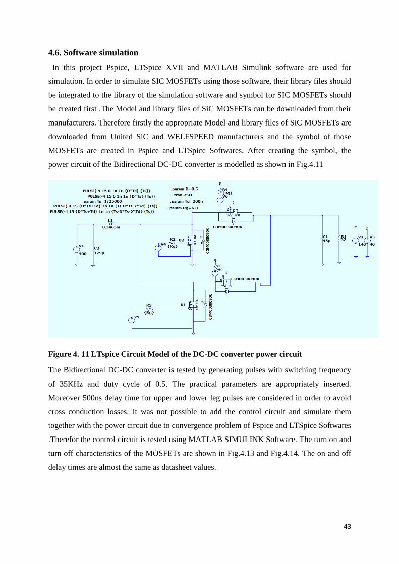
43
4.6. Software simulation
In this project Pspice, LTSpice XVII and MATLAB Simulink software are used for
simulation. In order to simulate SIC MOSFETs using those software, their library files should
be integrated to the library of the simulation software and symbol for SIC MOSFETs should
be created first .The Model and library files of SiC MOSFETs can be downloaded from their
manufacturers. Therefore firstly the appropriate Model and library files of SiC MOSFETs are
downloaded from United SiC and WELFSPEED manufacturers and the symbol of those
MOSFETs are created in Pspice and LTSpice Softwares. After creating the symbol, the
power circuit of the Bidirectional DC-DC converter is modelled as shown in Fig.4.11
Figure 4. 11 LTspice Circuit Model of the DC-DC converter power circuit
The Bidirectional DC-DC converter is tested by generating pulses with switching frequency
of 35KHz and duty cycle of 0.5. The practical parameters are appropriately inserted.
Moreover 500ns delay time for upper and lower leg pulses are considered in order to avoid
cross conduction losses. It was not possible to add the control circuit and simulate them
together with the power circuit due to convergence problem of Pspice and LTSpice Softwares
.Therefor the control circuit is tested using MATLAB SIMULINK Software. The turn on and
turn off characteristics of the MOSFETs are shown in Fig.4.13 and Fig.4.14. The on and off
delay times are almost the same as datasheet values.
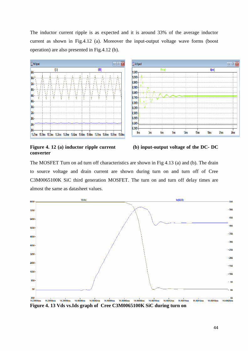
44
The inductor current ripple is as expected and it is around 33% of the average inductor
current as shown in Fig.4.12 (a). Moreover the input-output voltage wave forms (boost
operation) are also presented in Fig.4.12 (b).
Figure 4. 12 (a) inductor ripple current (b) input-output voltage of the DC- DC
converter
The MOSFET Turn on ad turn off characteristics are shown in Fig 4.13 (a) and (b). The drain
to source voltage and drain current are shown during turn on and turn off of Cree
C3M0065100K SiC third generation MOSFET. The turn on and turn off delay times are
almost the same as datasheet values.
Figure 4. 13 Vds vs.Ids graph of Cree C3M0065100K SiC during turn on
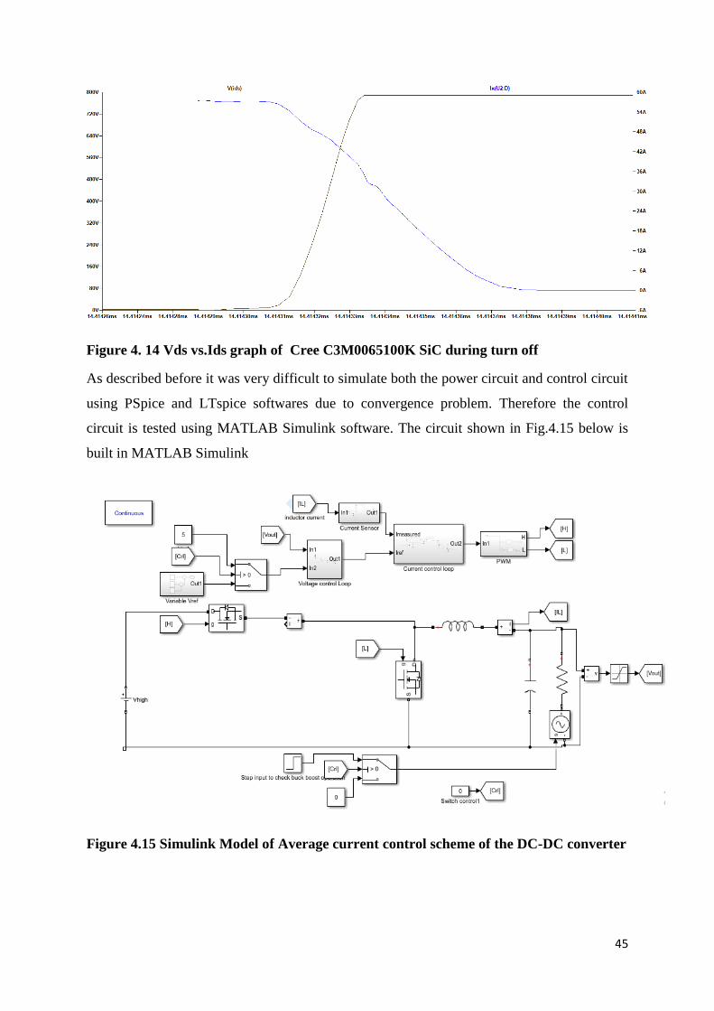
45
Figure 4. 14 Vds vs.Ids graph of Cree C3M0065100K SiC during turn off
As described before it was very difficult to simulate both the power circuit and control circuit
using PSpice and LTspice softwares due to convergence problem. Therefore the control
circuit is tested using MATLAB Simulink software. The circuit shown in Fig.4.15 below is
built in MATLAB Simulink
Figure 4.15 Simulink Model of Average current control scheme of the DC-DC converter
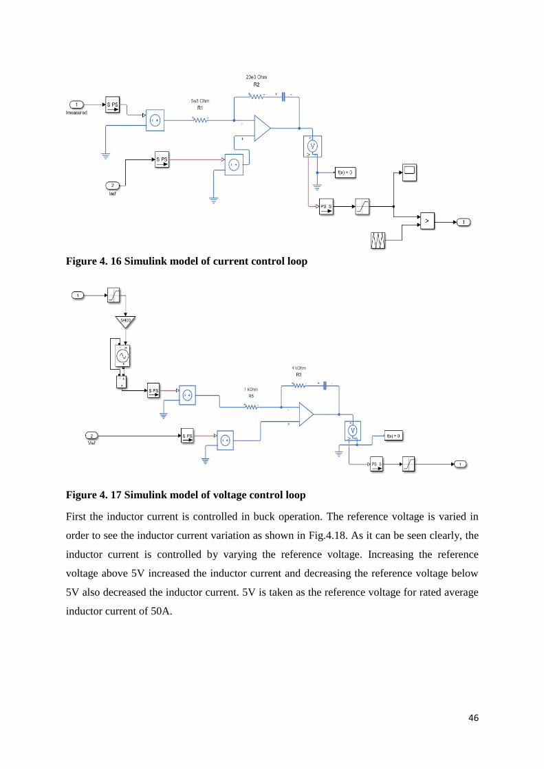
46
Figure 4. 16 Simulink model of current control loop
Figure 4. 17 Simulink model of voltage control loop
First the inductor current is controlled in buck operation. The reference voltage is varied in
order to see the inductor current variation as shown in Fig.4.18. As it can be seen clearly, the
inductor current is controlled by varying the reference voltage. Increasing the reference
voltage above 5V increased the inductor current and decreasing the reference voltage below
5V also decreased the inductor current. 5V is taken as the reference voltage for rated average
inductor current of 50A.
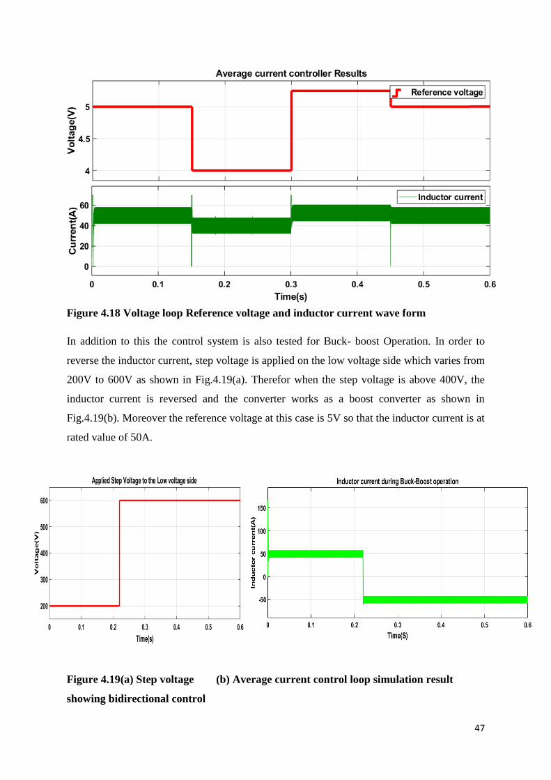
47
Figure 4.18 Voltage loop Reference voltage and inductor current wave form
In addition to this the control system is also tested for Buck- boost Operation. In order to
reverse the inductor current, step voltage is applied on the low voltage side which varies from
200V to 600V as shown in Fig.4.19(a). Therefor when the step voltage is above 400V, the
inductor current is reversed and the converter works as a boost converter as shown in
Fig.4.19(b). Moreover the reference voltage at this case is 5V so that the inductor current is at
rated value of 50A.
Figure 4.19(a) Step voltage (b) Average current control loop simulation result
showing bidirectional control
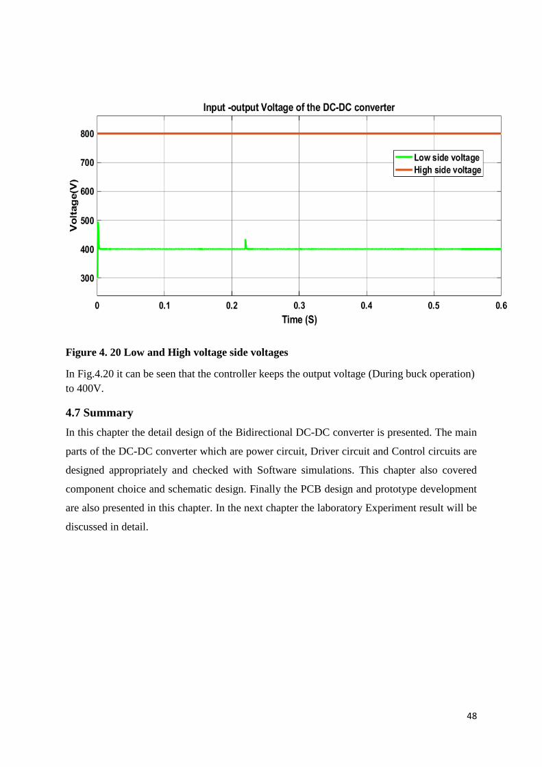
48
Figure 4. 20 Low and High voltage side voltages
In Fig.4.20 it can be seen that the controller keeps the output voltage (During buck operation)
to 400V.
4.7 Summary
In this chapter the detail design of the Bidirectional DC-DC converter is presented. The main
parts of the DC-DC converter which are power circuit, Driver circuit and Control circuits are
designed appropriately and checked with Software simulations. This chapter also covered
component choice and schematic design. Finally the PCB design and prototype development
are also presented in this chapter. In the next chapter the laboratory Experiment result will be
discussed in detail.

49
CHAPTER 5
5. RESULT AND DISCUSSION
5.1 Measuring Instruments
In the laboratory experiment, it is of interest to measure the drain-to-source voltage, the Gate-
to-source voltage, drain current, inductor current and input-output voltages. TDS 2024B
Oscilloscope from Tektronix is used to capture all waveforms. It has a bandwidth of 200MHz
and it is able to capture 2 GS/s. The Oscilloscope has four channels, which enable to measure
four different parameters at the same time. Moreover it has different triggering options and
complex mathematical operations.
In order to measure the Gate to source voltage, HAMEG instruments differential voltage
probe is used in order to protect grounding of the source terminal. It measures the voltage
difference between Gate and source terminals (since we have a negative turn off voltage).
Single-ended probe is not used because they measures voltage difference between a single
point and ground which in turn will ground the source terminal of the MOSFET. The drain to
source voltage is measured by using HP 10074A Probe. For measuring the inductor current,
TCP202 Current probe with 011606 Tektronix probe power supply is used. The gain of the
current probe is 0.76V/A
5.2 Power supplies
The gate driver circuit of the DC-DC converter needs 5V and 12V DC power supply.
Moreover small variable voltage DC power supply is required for testing the DC-DC
converter operation. FA-275 Triple power supply is used to supply the required voltages for
the gate driver circuit. It has 5V fixed output and 0-30V variable voltage output.
Another power supply used in this laboratory test is SUNZET 25. It has a capacity of
providing 25KW DC power with the voltage range of 0-1700V. This SUNZET power supply
has a USB port to be connected to the computer so that the output voltage and current can be
easily controlled and adjusted. In this lab test this power supply is used to supply power
during double pulse test and the final test of the DC-DC converter
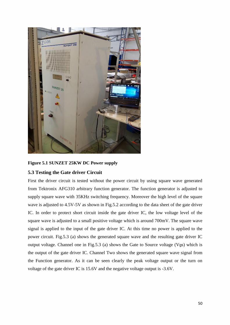
50
Figure 5.1 SUNZET 25KW DC Power supply
5.3 Testing the Gate driver Circuit
First the driver circuit is tested without the power circuit by using square wave generated
from Tektronix AFG310 arbitrary function generator. The function generator is adjusted to
supply square wave with 35KHz switching frequency. Moreover the high level of the square
wave is adjusted to 4.5V-5V as shown in Fig.5.2 according to the data sheet of the gate driver
IC. In order to protect short circuit inside the gate driver IC, the low voltage level of the
square wave is adjusted to a small positive voltage which is around 700mV. The square wave
signal is applied to the input of the gate driver IC. At this time no power is applied to the
power circuit. Fig.5.3 (a) shows the generated square wave and the resulting gate driver IC
output voltage. Channel one in Fig.5.3 (a) shows the Gate to Source voltage (Vgs) which is
the output of the gate driver IC. Channel Two shows the generated square wave signal from
the Function generator. As it can be seen clearly the peak voltage output or the turn on
voltage of the gate driver IC is 15.6V and the negative voltage output is -3.6V.
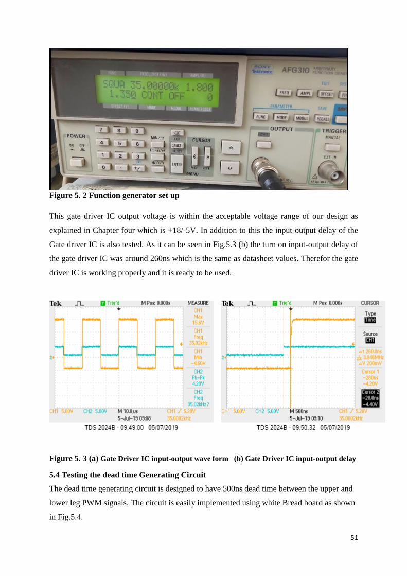
51
Figure 5. 2 Function generator set up
This gate driver IC output voltage is within the acceptable voltage range of our design as
explained in Chapter four which is +18/-5V. In addition to this the input-output delay of the
Gate driver IC is also tested. As it can be seen in Fig.5.3 (b) the turn on input-output delay of
the gate driver IC was around 260ns which is the same as datasheet values. Therefor the gate
driver IC is working properly and it is ready to be used.
Figure 5. 3 (a) Gate Driver IC input-output wave form (b) Gate Driver IC input-output delay
5.4 Testing the dead time Generating Circuit
The dead time generating circuit is designed to have 500ns dead time between the upper and
lower leg PWM signals. The circuit is easily implemented using white Bread board as shown
in Fig.5.4.
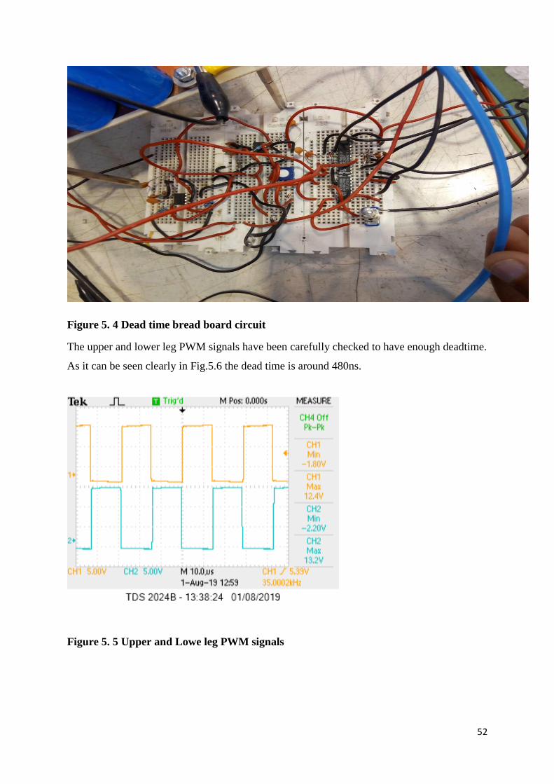
52
Figure 5. 4 Dead time bread board circuit
The upper and lower leg PWM signals have been carefully checked to have enough deadtime.
As it can be seen clearly in Fig.5.6 the dead time is around 480ns.
Figure 5. 5 Upper and Lowe leg PWM signals
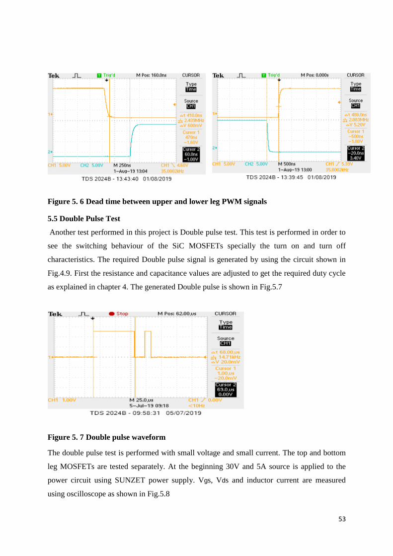
53
Figure 5. 6 Dead time between upper and lower leg PWM signals
5.5 Double Pulse Test
Another test performed in this project is Double pulse test. This test is performed in order to
see the switching behaviour of the SiC MOSFETs specially the turn on and turn off
characteristics. The required Double pulse signal is generated by using the circuit shown in
Fig.4.9. First the resistance and capacitance values are adjusted to get the required duty cycle
as explained in chapter 4. The generated Double pulse is shown in Fig.5.7
Figure 5. 7 Double pulse waveform
The double pulse test is performed with small voltage and small current. The top and bottom
leg MOSFETs are tested separately. At the beginning 30V and 5A source is applied to the
power circuit using SUNZET power supply. Vgs, Vds and inductor current are measured
using oscilloscope as shown in Fig.5.8
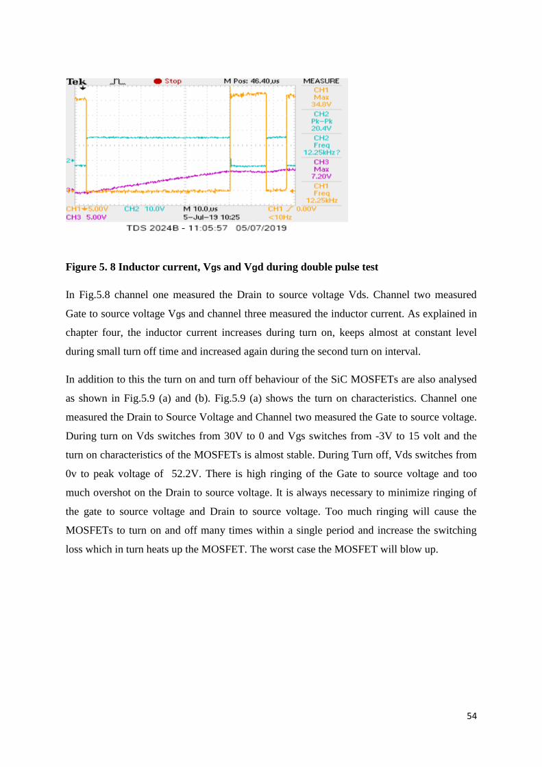
54
Figure 5. 8 Inductor current, Vgs and Vgd during double pulse test
In Fig.5.8 channel one measured the Drain to source voltage Vds. Channel two measured
Gate to source voltage Vgs and channel three measured the inductor current. As explained in
chapter four, the inductor current increases during turn on, keeps almost at constant level
during small turn off time and increased again during the second turn on interval.
In addition to this the turn on and turn off behaviour of the SiC MOSFETs are also analysed
as shown in Fig.5.9 (a) and (b). Fig.5.9 (a) shows the turn on characteristics. Channel one
measured the Drain to Source Voltage and Channel two measured the Gate to source voltage.
During turn on Vds switches from 30V to 0 and Vgs switches from -3V to 15 volt and the
turn on characteristics of the MOSFETs is almost stable. During Turn off, Vds switches from
0v to peak voltage of 52.2V. There is high ringing of the Gate to source voltage and too
much overshot on the Drain to source voltage. It is always necessary to minimize ringing of
the gate to source voltage and Drain to source voltage. Too much ringing will cause the
MOSFETs to turn on and off many times within a single period and increase the switching
loss which in turn heats up the MOSFET. The worst case the MOSFET will blow up.
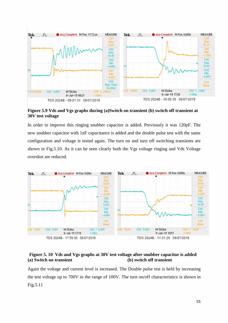
55
Figure 5.9 Vds and Vgs graphs during (a)Switch on transient (b) switch off transient at
30V test voltage
In order to improve this ringing snubber capacitor is added. Previously it was 120pF. The
new snubber capacitor with 1nF capacitance is added and the double pulse test with the same
configuration and voltage is tested again. The turn on and turn off switching transients are
shown in Fig.5.10. As it can be seen clearly both the Vgs voltage ringing and Vds Voltage
overshot are reduced.
Figure 5. 10 Vds and Vgs graphs at 30V test voltage after snubber capacitor is added
(a) Switch on transient (b) switch off transient
Again the voltage and current level is increased. The Double pulse test is held by increasing
the test voltage up to 700V in the range of 100V. The turn on/off characteristics is shown in
Fig.5.11
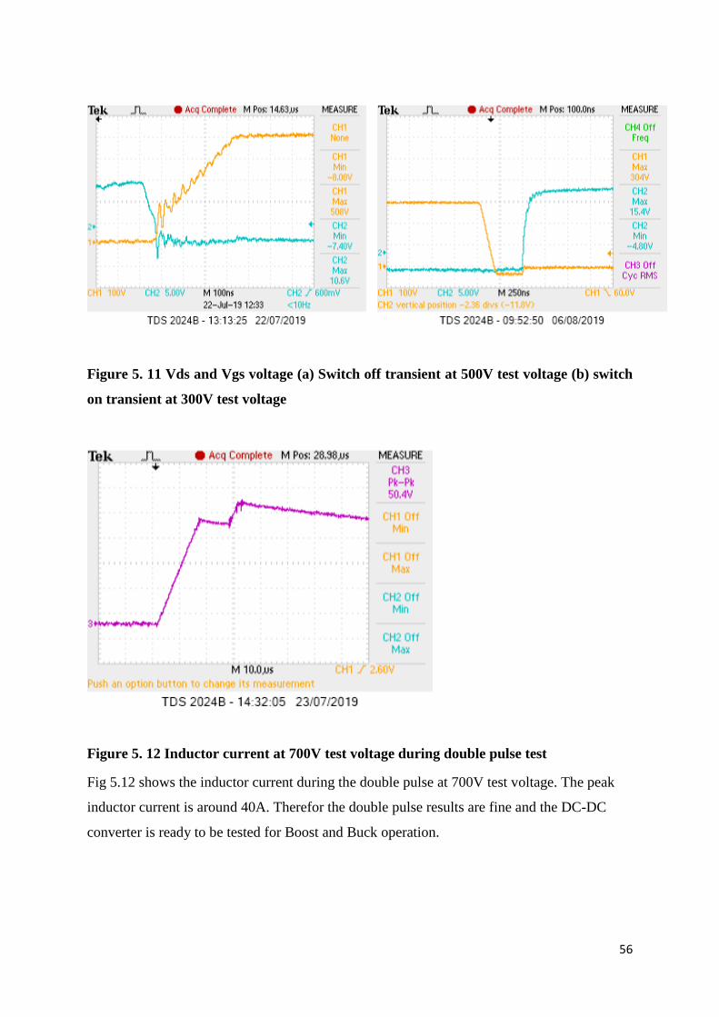
56
Figure 5. 11 Vds and Vgs voltage (a) Switch off transient at 500V test voltage (b) switch
on transient at 300V test voltage
Figure 5. 12 Inductor current at 700V test voltage during double pulse test
Fig 5.12 shows the inductor current during the double pulse at 700V test voltage. The peak
inductor current is around 40A. Therefor the double pulse results are fine and the DC-DC
converter is ready to be tested for Boost and Buck operation.
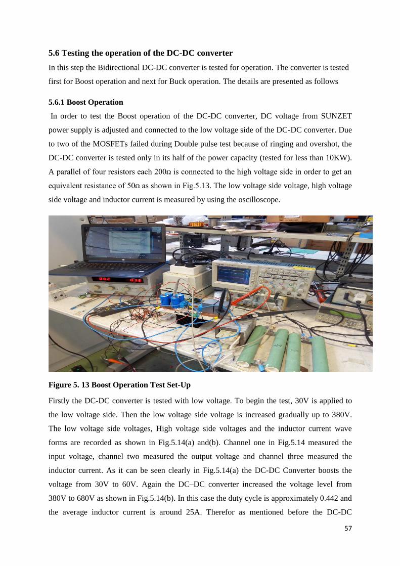
57
5.6 Testing the operation of the DC-DC converter
In this step the Bidirectional DC-DC converter is tested for operation. The converter is tested
first for Boost operation and next for Buck operation. The details are presented as follows
5.6.1 Boost Operation
In order to test the Boost operation of the DC-DC converter, DC voltage from SUNZET
power supply is adjusted and connected to the low voltage side of the DC-DC converter. Due
to two of the MOSFETs failed during Double pulse test because of ringing and overshot, the
DC-DC converter is tested only in its half of the power capacity (tested for less than 10KW).
A parallel of four resistors each 200ꭥ is connected to the high voltage side in order to get an
equivalent resistance of 50ꭥ as shown in Fig.5.13. The low voltage side voltage, high voltage
side voltage and inductor current is measured by using the oscilloscope.
Figure 5. 13 Boost Operation Test Set-Up
Firstly the DC-DC converter is tested with low voltage. To begin the test, 30V is applied to
the low voltage side. Then the low voltage side voltage is increased gradually up to 380V.
The low voltage side voltages, High voltage side voltages and the inductor current wave
forms are recorded as shown in Fig.5.14(a) and(b). Channel one in Fig.5.14 measured the
input voltage, channel two measured the output voltage and channel three measured the
inductor current. As it can be seen clearly in Fig.5.14(a) the DC-DC Converter boosts the
voltage from 30V to 60V. Again the DC–DC converter increased the voltage level from
380V to 680V as shown in Fig.5.14(b). In this case the duty cycle is approximately 0.442 and
the average inductor current is around 25A. Therefor as mentioned before the DC-DC
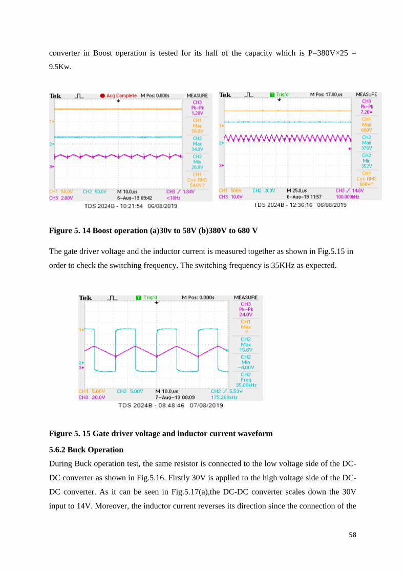
58
converter in Boost operation is tested for its half of the capacity which is P=380V×25 =
9.5Kw.
Figure 5. 14 Boost operation (a)30v to 58V (b)380V to 680 V
The gate driver voltage and the inductor current is measured together as shown in Fig.5.15 in
order to check the switching frequency. The switching frequency is 35KHz as expected.
Figure 5. 15 Gate driver voltage and inductor current waveform
5.6.2 Buck Operation
During Buck operation test, the same resistor is connected to the low voltage side of the DC-
DC converter as shown in Fig.5.16. Firstly 30V is applied to the high voltage side of the DC-
DC converter. As it can be seen in Fig.5.17(a),the DC-DC converter scales down the 30V
input to 14V. Moreover, the inductor current reverses its direction since the connection of the
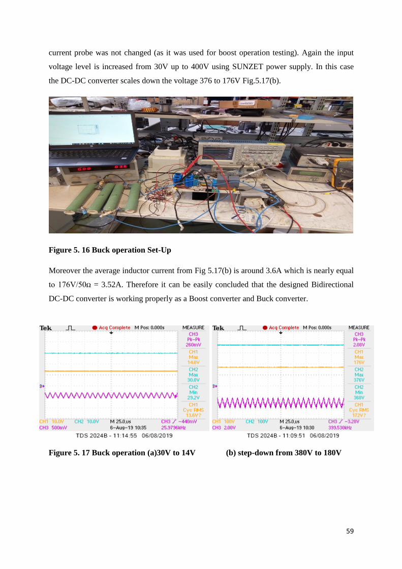
59
current probe was not changed (as it was used for boost operation testing). Again the input
voltage level is increased from 30V up to 400V using SUNZET power supply. In this case
the DC-DC converter scales down the voltage 376 to 176V Fig.5.17(b).
Figure 5. 16 Buck operation Set-Up
Moreover the average inductor current from Fig 5.17(b) is around 3.6A which is nearly equal
to 176V/50ꭥ = 3.52A. Therefore it can be easily concluded that the designed Bidirectional
DC-DC converter is working properly as a Boost converter and Buck converter.
Figure 5. 17 Buck operation (a)30V to 14V (b) step-down from 380V to 180V

60
CHAPTER 6
6. CONCLUSION AND FUTURE WORK
6.1 Conclusion
In this thesis work the design of 20KW Bidirectional DC-DC converter is presented. The DC-
DC converter has a capacity of 20KW and designed using Silicon Carbide MOSFETs. The
step by step design procedures, design Considerations and Mathematical calculations have
been presented. The three main parts of the DC-DC converter which are the power circuit,
driver circuit and Control circuit are designed properly. In addition to this the PCB design
and prototype development was also a part of this thesis work.
In this thesis work both software simulation and laboratory experiment results are discussed
briefly. LTspice, PSpice and MATLAB Simulink software are used for simulation. The
laboratory experiment results are presented in step by step. First the driver circuit is tested by
generating square wave from function generators. Next double pulse test have been
performed on the DC-DC converter. Finally the Buck and Boost operation of the DC-DC
converter is presented in detail.
Both the laboratory and simulation result shows that the designed Bidirectional DC- DC
converter performed as expected. The double pulse test results are fine. The DC-DC
converter boosts the voltage from 380V to 680V during Boost operation and it step down the
376V to 176V during Buck operation. Moreover the designed DC-DC converter is much
smaller in size compared to the conventional 25KW SUNZET DC Power supply.
6.2 Future Work
This thesis work is a part of “Silicon Carbide Solutions” project which is funded by
BASQUE GOVERNMENT and EUROPEAN UNION through the European Regional
Development Fund 2014-2020 at Zigor Corporation. In this project, Zigor Corporation would
like to become familiarize with SiC materials and manufacture power converters using this
advanced power electronics devices. The main goal of the project is to manufacture solar
inverters using SiC technology with less size and better efficiency. This thesis work is the
beginning of the project since DC-DC converters are required to integrate PV panels with

61
solar inverters. Zigor Corporation also wants to test and manufacture power converters with
high switching frequency and low cost. Therefore the future works will include
Improving the switching frequency to 100KHz
Minimizing Cost of the project
Development of solar inverters using Silicon carbide technologies
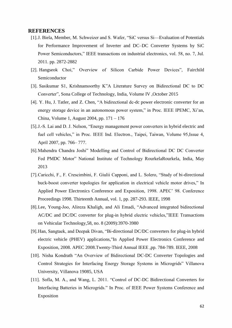
62
REFERENCES
[1]. J. Biela, Member, M. Schweizer and S. Wafer, “SiC versus Si—Evaluation of Potentials
for Performance Improvement of Inverter and DC–DC Converter Systems by SiC
Power Semiconductors,” IEEE transactions on industrial electronics, vol. 58, no. 7, Jul.
2011. pp. 2872-2882
[2]. Hangseok Choi,” Overview of Silicon Carbide Power Devices”, Fairchild
Semiconductor
[3]. Sasikumar S1, Krishnamoorthy K”A Literature Survey on Bidirectional DC to DC
Converter”, Sona College of Technology, India, Volume IV ,October 2015
[4]. Y. Hu, J. Tatler, and Z. Chen, “A bidirectional dc-dc power electronic converter for an
energy storage device in an autonomous power system,” in Proc. IEEE IPEMC, Xi’an,
China, Volume 1, August 2004, pp. 171 – 176
[5]. J.-S. Lai and D. J. Nelson, “Energy management power converters in hybrid electric and
fuel cell vehicles,” in Proc. IEEE Ind. Electron., Taipei, Taiwan, Volume 95,Issue 4,
April 2007, pp. 766– 777.
[6]. Mahendra Chandra Joshi” Modelling and Control of Bidirectional DC DC Converter
Fed PMDC Motor” National Institute of Technology RourkelaRourkela, India, May
2013
[7]. Caricchi, F., F. Crescimbini, F. Giulii Capponi, and L. Solero, “Study of bi-directional
buck-boost converter topologies for application in electrical vehicle motor drives,” In
Applied Power Electronics Conference and Exposition, 1998. APEC’ 98. Conference
Proceedings 1998. Thirteenth Annual, vol. 1, pp. 287-293. IEEE, 1998
[8]. Lee, Young-Joo, Alireza Khaligh, and Ali Emadi, “Advanced integrated bidirectional
AC/DC and DC/DC converter for plug-in hybrid electric vehicles,”IEEE Transactions
on Vehicular Technology,58, no. 8 (2009):3970-3980
[9]. Han, Sangtaek, and Deepak Divan, “Bi-directional DC/DC converters for plug-in hybrid
electric vehicle (PHEV) applications,"In Applied Power Electronics Conference and
Exposition, 2008. APEC 2008.Twenty-Third Annual IEEE ,pp. 784-789. IEEE, 2008
[10]. Nisha Kondrath “An Overview of Bidirectional DC-DC Converter Topologies and
Control Strategies for Interfacing Energy Storage Systems in Microgrids” Villanova
University, Villanova 19085, USA
[11]. Sofla, M. A., and Wang, L. 2011. “Control of DC-DC Bidirectional Converters for
Interfacing Batteries in Microgrids.” In Proc. of IEEE Power Systems Conference and
Exposition

63
[12]. Inoue, S., and Akagi, H. 2007. “A Bidirectional DC-DC Converter for an Energy
Storage System with Galvanic Isolation.” IEEE Transactions on Power Electronics 22
(6): 2299-306
[13]. Kondrath, N. 2017. “Design and Evaluation of a Novel Hybrid Sic-Gan Based
Bidirectional Full-Bridge DC-DC Converter.” SAE Technical Paper 2017-01-
2032.doi:10.4271/2017-01-2032
[14]. Liu, L-Y., Tsai, M-C., Hsu, C-L., Lo, K-Y., and Chang, Y-R. 2015. “Design of a
Energy Storage Converter for Micro-grid Applications.” In Proceedings of 4th
International Conference on Renewable Energy Research and Applications.
[15]. Hamid R. Karshenas, Hamid Daneshpajooh, Alireza Safaee, Praveen Jain and Alireza
Bakhshai (2011).Bidirectional DC - DC Converters for Energy Storage Systems, Energy
Storage in the Emerging Era of Smart Grids, Prof. Rosario Carbone (Ed.), ISBN: 978-
953-307-269-2, InTech, Available from:http://www.intechopen.com/books/energy-
storage-in-the-emerging-era-of-smart-grids/bidirectional-dc-dcconverters-for-energy-
storage-systems
[16]. Getnet Tadesse,(2015).Challenges of Multichannel Interleaved Bidirectional Power
converters and their digital solutions (Unpublished Master’s thesis).University of
Nottingham, Nottingham ,United Kingdom
[17]. Julius Rice, John Mookken “SiC MOSFET Gate Drive Design Considerations”, Cree
Inc. Durham, NC United States
[18]. Rohm. Gate driver selection Guide
[19]. Infineon EiceDRIVER™ gate driver ICs Selection guide 2019
[20]. Infineon .Advanced Gate Drive Options for Silicon Carbide (SiC) MOSFETs using
EiceDRIVER™,2018.
[21]. Texas Instruments. Current Mode Control in Switching Power Supplies
[22]. Texas Instruments. Impact of an isolated gate driver
[23]. On Semiconductor. “SiC MOSFETs Gate driver Optimization”. Rev. 1, July – 2018
[24]. Cree Inc . Gate Driver for Cree’s Generation 3 (C3MTM) SiC MOSFET. Application
Note
[25]. SiC MOSFET, C3M0065100K datasheet, Wolfspeed Cree
[26]. Rosario Gerhardt, “ProPerties and applications of silicon carbide”, InTech ,Janeza
Trdine 9, 51000 Rijeka, Croatia, March 2011

64
[27]. Bendik Nybakk Torsæter ,(2016). Evaluation of Switching Characteristics,Switching
Losses and Snubber Design for a Full SiC Half-Bridge Power Module (Unpublished
Master’s thesis). Norwegian University of Science and Technology, Norway
[28]. Sanket Sapre “Isolated Gate Drivers—What, Why, and How?”, Analog Devices.
Analog Dialogue 52-06, June 2018
[29]. Toshiba.Power MOSFET Characterstics
[30]. Lloyd Dixon. “Average Current Mode Control of Switching Power
Supplies”.UNITRODE Application Notes. Texas instruments
[31]. Henry J. Zhang. “PCB Layout Considerations for Non-Isolated Switching Power
Supplies”. Linear technology. Application Note 136.June 2012