Embed Size (px)
Citation preview
University of Notre Dame Center for Nano Science and Technology
Gregory L. SniderDepartment of Electrical Engineering
University of Notre Dame
Nanoelectronic Devices

University of Notre Dame Center for Nano Science and Technology
What are Nanoelectronic Devices?
A rough definition is a device where:
• The wave nature of electrons plays a significant
(dominant) role.
• The quantized nature of charge plays a significant
role.

University of Notre Dame Center for Nano Science and Technology
Examples
• Quantum point contacts (QPC)
• Resonant tunneling diodes (RTD)
• Single-electron devices
• Quantum-dot Cellular Automata (QCA)
• Molecular electronics (sometimes not truly nano)

University of Notre Dame Center for Nano Science and Technology
References
• Single Charge Tunneling, H. Grabet and M. Devoret, Plenum
Press, New York, 1992
• Modern Semiconductor Devices, S.M. Sze, John Wiley and Sons,
New York, 1998
• Theory of Modern Electronic Semiconductor Devices, K. Brennan
and A. Brown, John Wiley and Sons, New York, 2002
• Quantum Semiconductor Structures, Fundamentals and
Applications , C. Weisbuch and B. Vinter, Academic Press, Inc.,
San Diego, 1991

University of Notre Dame Center for Nano Science and Technology
When does Quantum Mechanics Play a Role?
W & V, pg. 12, Fig. 5
University of Notre Dame Center for Nano Science and Technology
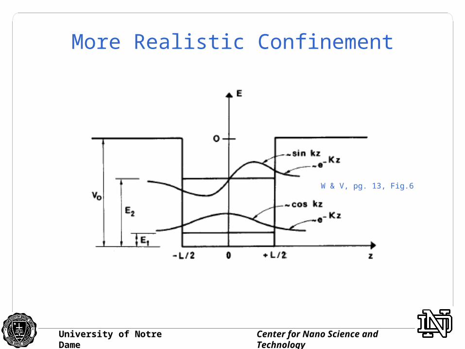
More Realistic Confinement
W & V, pg. 13, Fig.6
University of Notre Dame Center for Nano Science and Technology
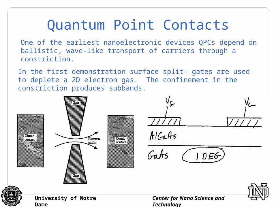
Quantum Point ContactsOne of the earliest nanoelectronic devices QPCs depend on ballistic, wave-like transport of carriers through a constriction.
In the first demonstration surface split- gates are used to deplete a 2D electron gas. The confinement in the constriction produces subbands.
University of Notre Dame Center for Nano Science and Technology
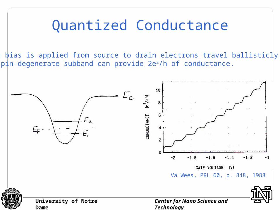
Quantized Conductance
When a bias is applied from source to drain electrons travel ballisticly.Each spin-degenerate subband can provide 2e2/h of conductance.
Va Wees, PRL 60, p. 848, 1988
University of Notre Dame Center for Nano Science and Technology
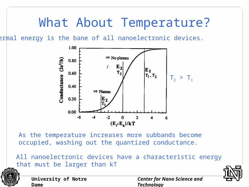
What About Temperature?Thermal energy is the bane of all nanoelectronic devices.
As the temperature increases more subbands become occupied, washing out the quantized conductance.
T2 > T1
All nanoelectronic devices have a characteristic energy that must be larger than kT
University of Notre Dame Center for Nano Science and Technology
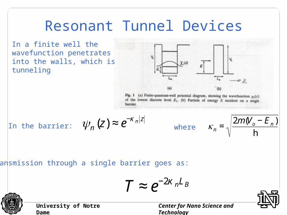
Resonant Tunnel DevicesIn a finite well the wavefunction penetrates into the walls, which is tunneling
€
ψn (z) ≈ e−κ n zIn the barrier:
€
κn =2m(Vo − En )
hwhere
Transmission through a single barrier goes as:
€
T ≈ e−2κ nLB
University of Notre Dame Center for Nano Science and Technology
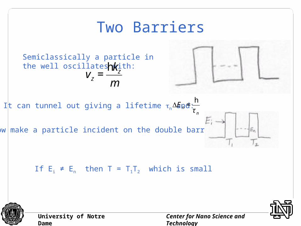
Two Barriers
Semiclassically a particle in the well oscillates with:
€
vz =hkzm
It can tunnel out giving a lifetime n and:
€
ΔEn =h
τ n
Now make a particle incident on the double barrier:
If Ei ≠ En then T = T1T2 which is small
University of Notre Dame Center for Nano Science and Technology
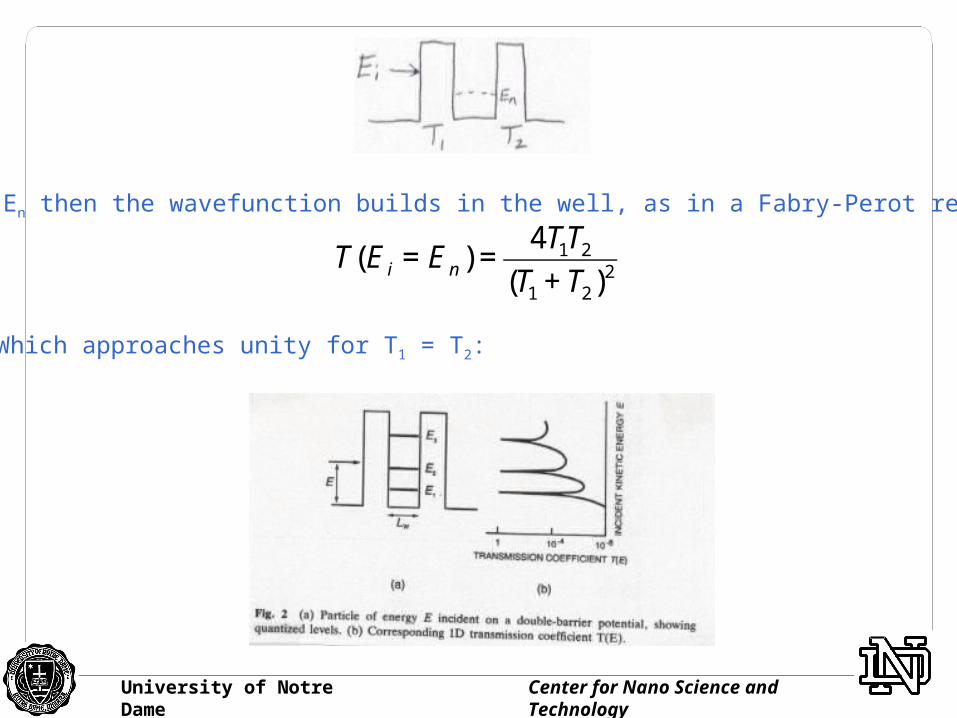
If Ei = En then the wavefunction builds in the well, as in a Fabry-Perot resonator:
€
T(E i = En ) =4T1T2
(T1 + T2)2
Which approaches unity for T1 = T2:
University of Notre Dame Center for Nano Science and Technology
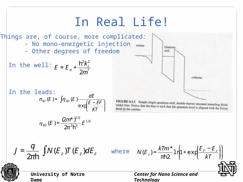
In Real Life!Things are, of course, more complicated:
- No mono-energetic injection- Other degrees of freedom
In the well:
€
E = En +h2k⊥
2
2m*
In the leads:
€
n3D (E) = η 3D (E)dE
expE − EF
KT
⎛
⎝ ⎜
⎞
⎠ ⎟
∫
€
η3D (E) =(2m*)3 / 2
2π 2h3E1/ 2
€
J =q
2πhN(E z)T(E z)dE z∫ where
€
N(E z) =kTm *
πh2ln 1+ exp
EF − E zkT
⎛
⎝ ⎜
⎞
⎠ ⎟
⎛
⎝ ⎜
⎞
⎠ ⎟

University of Notre Dame Center for Nano Science and Technology
In k Space No One Can Hear You Scream!
For Transmission:
€
kzo =2m * (Eo − Ec
L )
h
To get through the barriers electrons must have E > Ec but must also have the correct kz. Only states on the disk meet these criteria.

University of Notre Dame Center for Nano Science and Technology
J is proportional to the number of states on the disk, and therefore to the area of the disk:
€
Area = πR2 = π kF2 − kzo
2( )
€
⇒ J ∝ kF2 − kzo
2 ∝ EFL − Ec
L( ) − Eo − Ec
L( ) = EF
L − Eo
€
∴ J ∝V
EcL is above Eo, so no
states have the correct kz
Note: we have ignored the transmission probability

University of Notre Dame Center for Nano Science and Technology
ScatteringScattering plays an important but harmful role, mixing in-plane and perpendicular states
B&B p236
University of Notre Dame Center for Nano Science and Technology
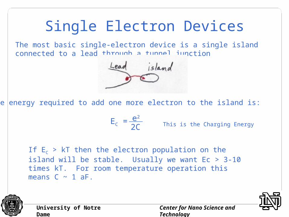
Single Electron DevicesThe most basic single-electron device is a single island connected to a lead through a tunnel junction
The energy required to add one more electron to the island is:
EC = e2
2C This is the Charging Energy
If EC > kT then the electron population on the island will be stable. Usually we want Ec > 3-10 times kT. For room temperature operation this means C ~ 1 aF.
University of Notre Dame Center for Nano Science and Technology
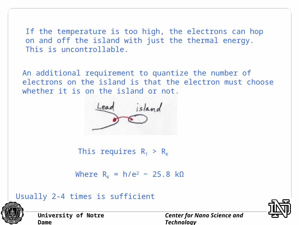
If the temperature is too high, the electrons can hop on and off the island with just the thermal energy. This is uncontrollable.
An additional requirement to quantize the number of electrons on the island is that the electron must choose whether it is on the island or not.
This requires RT > RK
Where RK = h/e2 ~ 25.8 kΩ
Usually 2-4 times is sufficient
University of Notre Dame Center for Nano Science and Technology
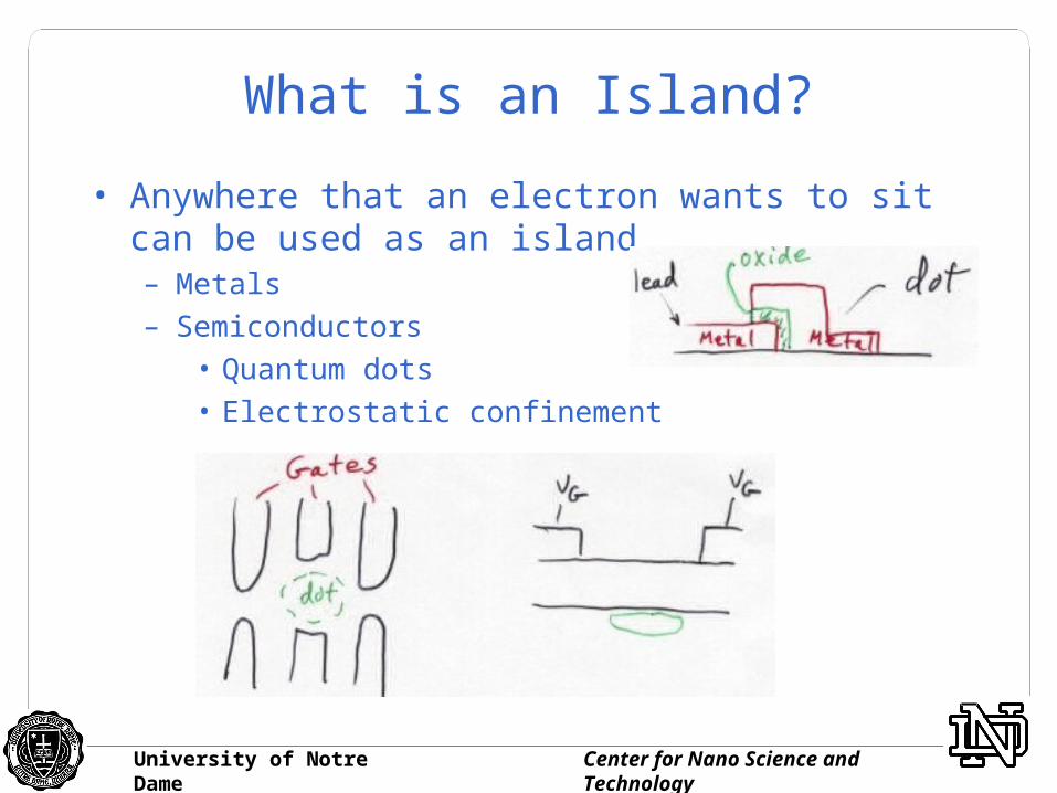
What is an Island?
• Anywhere that an electron wants to sit can be used as an island– Metals– Semiconductors
• Quantum dots• Electrostatic confinement
University of Notre Dame Center for Nano Science and Technology
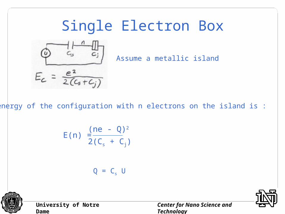
Single Electron Box
Assume a metallic island
The energy of the configuration with n electrons on the island is :
E(n) = (ne - Q)2
2(Cs + Cj)
Q = Cs U
University of Notre Dame Center for Nano Science and Technology
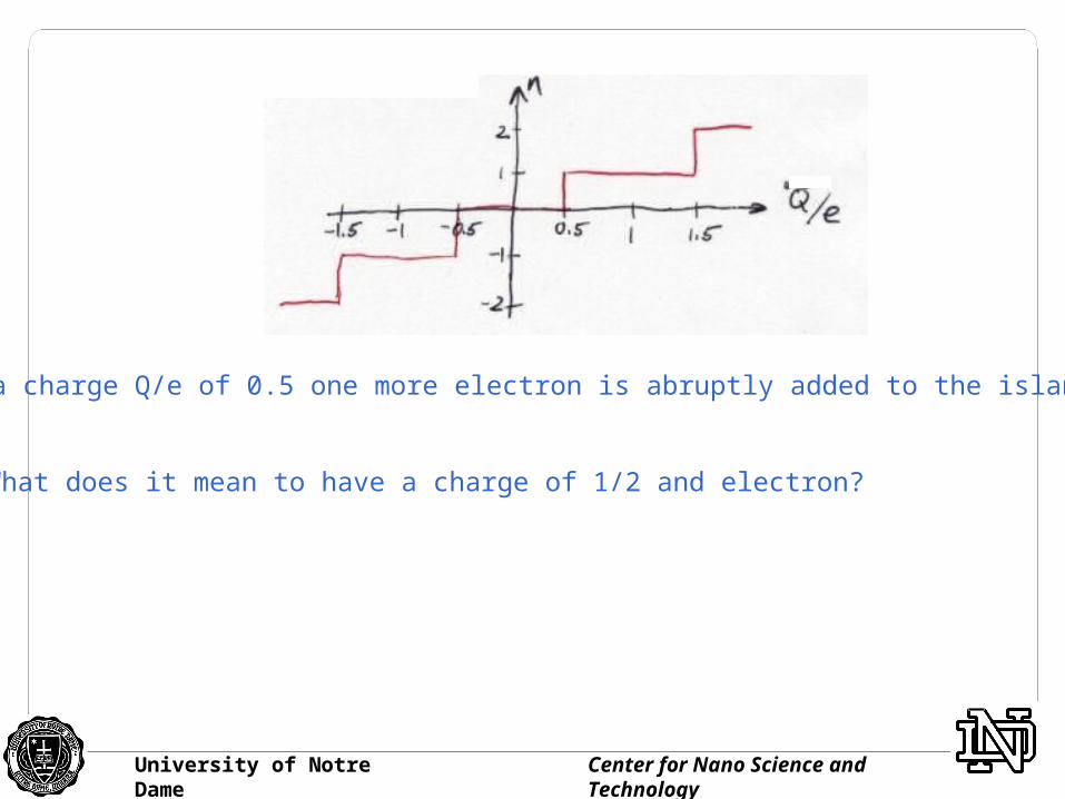
At a charge Q/e of 0.5 one more electron is abruptly added to the island.
What does it mean to have a charge of 1/2 and electron?
University of Notre Dame Center for Nano Science and Technology
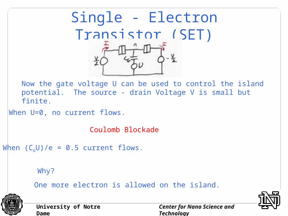
Single - Electron Transistor (SET)
Now the gate voltage U can be used to control the island potential. The source - drain Voltage V is small but finite.
When U=0, no current flows.
Coulomb Blockade
When (CGU)/e = 0.5 current flows.
Why?
One more electron is allowed on the island.
University of Notre Dame Center for Nano Science and Technology
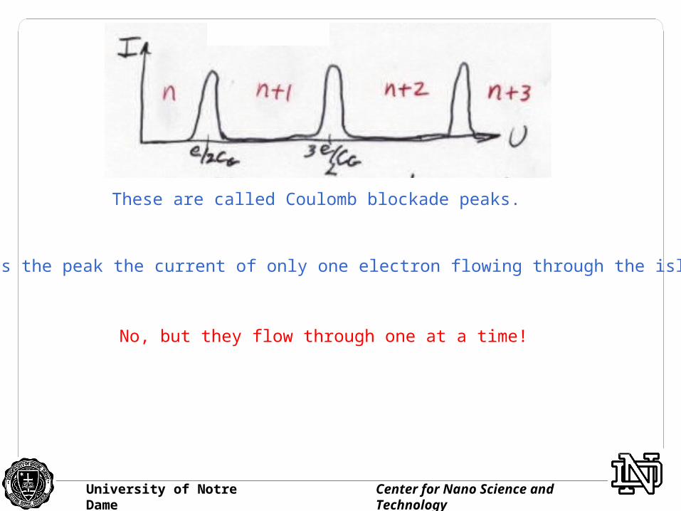
These are called Coulomb blockade peaks.
Is the peak the current of only one electron flowing through the island?
No, but they flow through one at a time!

University of Notre Dame Center for Nano Science and Technology
What about Temperature?
G&D p181
As the temperature increases the peaks stay about the same, while the valleys no longer go to zero. This is the loss of Coulomb blockade. Finally the peaks smear out entirely.
This shows the classical regime, such as for metal dots. In semiconductor dots resonant can cause an increase in the conductance at low temperatures (the peak values increase).
University of Notre Dame Center for Nano Science and Technology
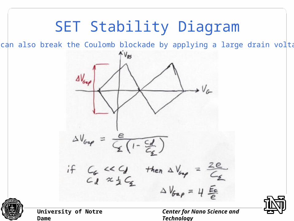
SET Stability DiagramYou can also break the Coulomb blockade by applying a large drain voltage.
University of Notre Dame Center for Nano Science and Technology
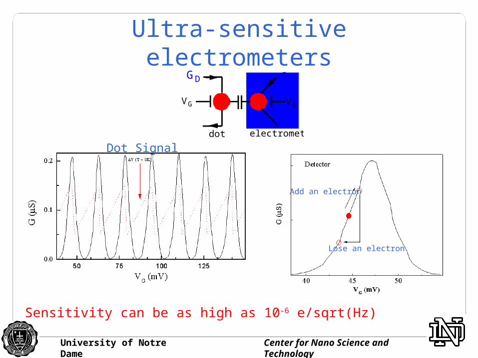
Ultra-sensitive electrometers
Dot Signal
Add an electron
Lose an electron
GD GE
VG VE
dot electrometer
Sensitivity can be as high as 10-6 e/sqrt(Hz)
University of Notre Dame Center for Nano Science and Technology
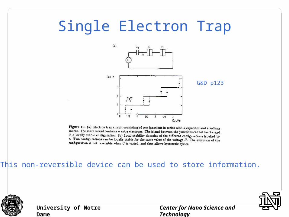
Single Electron Trap
G&D p123
This non-reversible device can be used to store information.

University of Notre Dame Center for Nano Science and Technology
Single Electron Turnstile
G&D p124
This is an extension of the single electron trap that can move electrons one at at time

University of Notre Dame Center for Nano Science and Technology
Turnstile Operation
G&D page 125Why does it need to be non-reversible?
Can this be used as a current standard?
Issues:Co-tunnelingMissed transitionsThermally activated events
University of Notre Dame Center for Nano Science and Technology
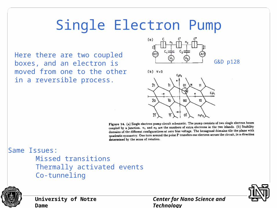
Single Electron Pump
G&D p128Here there are two coupled boxes, and an electron is moved from one to the other in a reversible process.
Same Issues:Missed transitionsThermally activated eventsCo-tunneling
University of Notre Dame Center for Nano Science and Technology
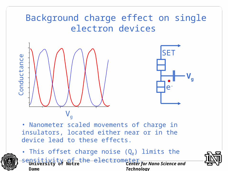
e-
Vg
SET
Con
duct
ance
Vg
• Nanometer scaled movements of charge in insulators, located either near or in the device lead to these effects.
• This offset charge noise (Q0) limits the sensitivity of the electrometer.
Background charge effect on single electron devices
University of Notre Dame Center for Nano Science and Technology
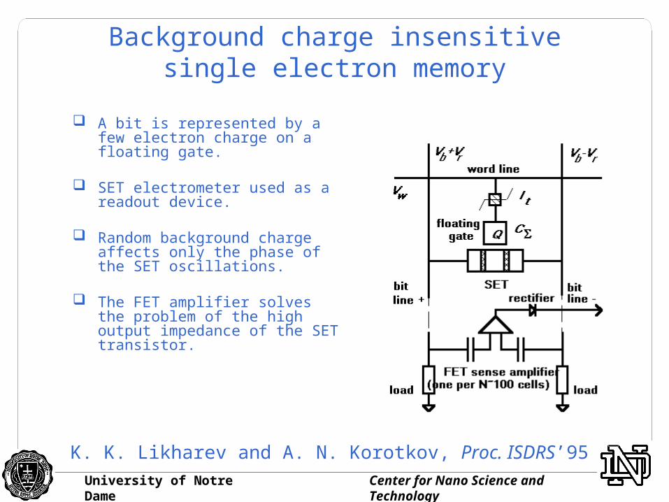
Background charge insensitive single electron memory
A bit is represented by a few electron charge on a floating gate.
SET electrometer used as a readout device.
Random background charge affects only the phase of the SET oscillations.
The FET amplifier solves the problem of the high output impedance of the SET transistor.
K. K. Likharev and A. N. Korotkov, Proc. ISDRS’95
University of Notre Dame Center for Nano Science and Technology
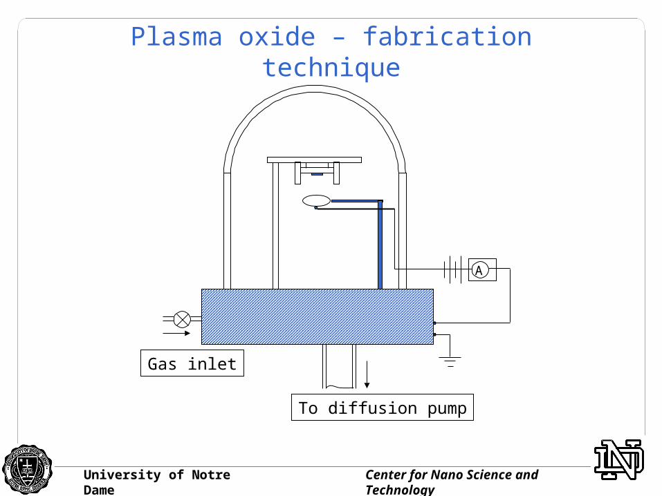
Plasma oxide – fabrication technique
A
To diffusion pump
Gas inlet

University of Notre Dame Center for Nano Science and Technology
Plasma oxide device
• Two step e-beam lithography on PMMA/MMA.
• Oxidation after first step in oxygen plasma formed by glow discharge.
• Oxide thickness characterized by VASE technique.
CG FG
Ground
BG
SET
• 6 nm of oxide grown after 5 min oxidation in 50 mTorr oxygen plasma at 10 W.

University of Notre Dame Center for Nano Science and Technology
Hysteresis Loops
• SET conductance monitored on the application of a bias on the control gate.
• A back gate bias cancels the direct effect of the control gate on the SET.
• The change in the operating point of the SET is due to electrons charging and discharging the floating gate.
University of Notre Dame Center for Nano Science and Technology
on=“1”
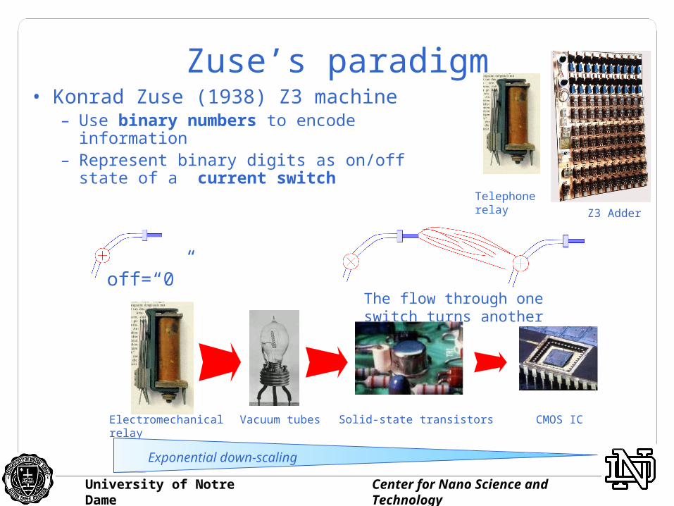
Zuse’s paradigm• Konrad Zuse (1938) Z3 machine
– Use binary numbers to encode information
– Represent binary digits as on/off state of a current switch Telephone
relay Z3 Adder
The flow through one switch turns another on or off.
Electromechanicalrelay
Exponential down-scaling
Vacuum tubes Solid-state transistors CMOS IC
off=“0”

University of Notre Dame Center for Nano Science and Technology
Problems shrinking the current-switch
Electromechanicalrelay
Vacuum tubes Solid-state transistors CMOS IC
New idea
Valve shrinks also – hard to get good on/off
Current becomes small - resistance becomes high Hard to turn next switchCharge becomes quantized
Power dissipation threatens to melt the chip.
Quantum Dots
University of Notre Dame Center for Nano Science and Technology
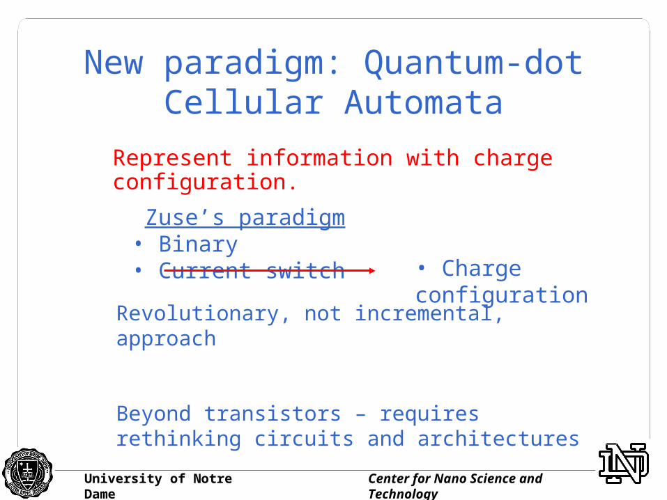
New paradigm: Quantum-dot Cellular Automata
Revolutionary, not incremental, approach
Beyond transistors – requires rethinking circuits and architectures
Represent information with charge configuration.
Zuse’s paradigm• Binary• Current switch • Charge configuration
University of Notre Dame Center for Nano Science and Technology
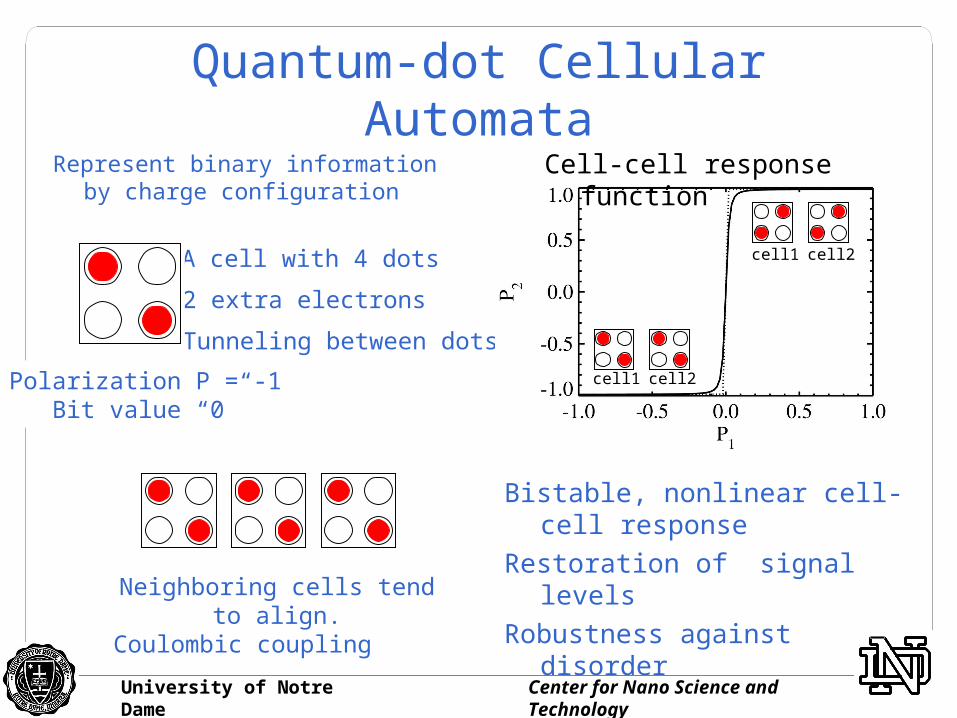
Quantum-dot Cellular Automata
Represent binary information by charge configuration
A cell with 4 dots
Tunneling between dots
Polarization P = +1Bit value “1”
2 extra electrons
Polarization P = -1Bit value “0”
Bistable, nonlinear cell-cell response
Restoration of signal levels
Robustness against disorder
cell1 cell2
cell1 cell2
Cell-cell response function
Neighboring cells tend to align.Coulombic coupling
University of Notre Dame Center for Nano Science and Technology
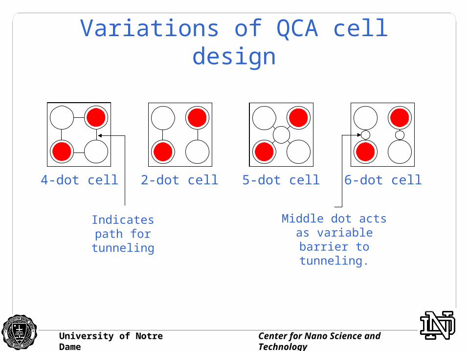
Variations of QCA cell design
4-dot cell 2-dot cell 5-dot cell 6-dot cell
Middle dot acts as variable barrier to
tunneling.
Indicates path for tunneling
University of Notre Dame Center for Nano Science and Technology
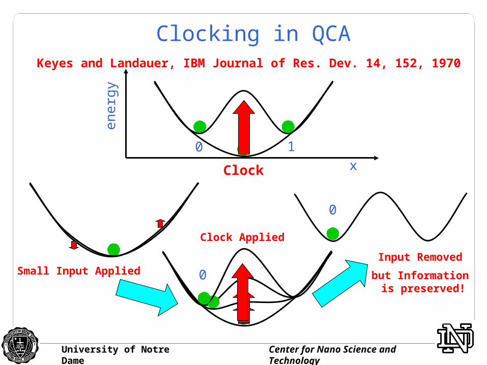
Clocking in QCA
0 1
0
en
erg
y
xClock
Small Input Applied
Clock Applied
Input Removed
but Information is preserved!
0
Keyes and Landauer, IBM Journal of Res. Dev. 14, 152, 1970
University of Notre Dame Center for Nano Science and Technology
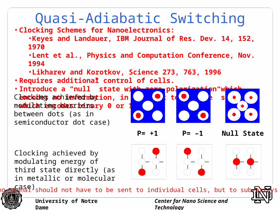
Quasi-Adiabatic Switching• Clocking Schemes for Nanoelectronics:
•Keyes and Landauer, IBM Journal of Res. Dev. 14, 152, 1970•Lent et al., Physics and Computation Conference, Nov. 1994•Likharev and Korotkov, Science 273, 763, 1996
• Requires additional control of cells.• Introduce a “null” state with zero polarization which encodes no
information, in contrast to “active” state which encodes binary 0 or 1.
Clocking achieved by modulating energy of third state directly (as in metallic or molecular case)
P= +1 P= –1 Null State
Clocking achieved by modulating barriers between dots (as in semiconductor dot case)
Clocking signal should not have to be sent to individual cells, but to sub-arrays of cells.
University of Notre Dame Center for Nano Science and Technology
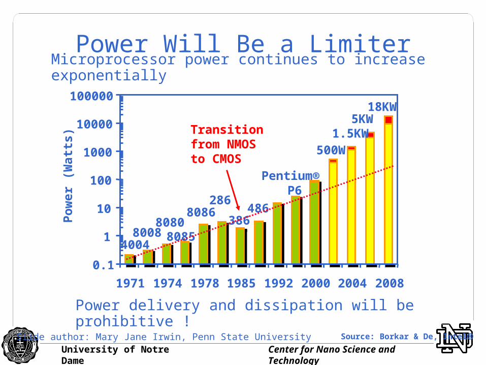
Power Will Be a Limiter
5KW 18KW
1.5KW 500W
40048008
80808085
8086286
386486
Pentium®
0.1
1
10
100
1000
10000
100000
1971 1974 1978 1985 1992 2000 2004 2008
Pow
er
(Watt
s)
Microprocessor power continues to increase exponentially
Power delivery and dissipation will be prohibitive !
P6
Transition from NMOS to CMOS
Source: Borkar & De, IntelSlide author: Mary Jane Irwin, Penn State University
University of Notre Dame Center for Nano Science and Technology
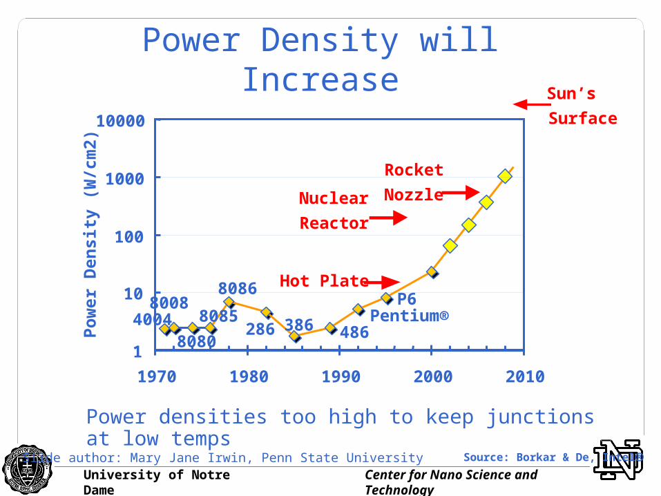
Power Density will Increase
40048008
8080
8085
8086
286 386 486Pentium®
P6
1
10
100
1000
10000
1970 1980 1990 2000 2010
Pow
er
Den
sit
y (
W/c
m2)
Hot Plate
Nuclear
Reactor
Rocket
Nozzle
Power densities too high to keep junctions at low temps
Source: Borkar & De, Intel
Sun’s
Surface
Slide author: Mary Jane Irwin, Penn State University
University of Notre Dame Center for Nano Science and Technology
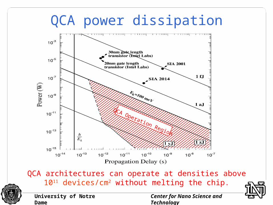
QCA power dissipation
QCA architectures can operate at densities above 1011 devices/cm2 without melting the chip.
QCA Operation Region
University of Notre Dame Center for Nano Science and Technology
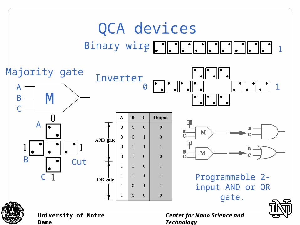
0 01 1
01 10
A
B
C
Out
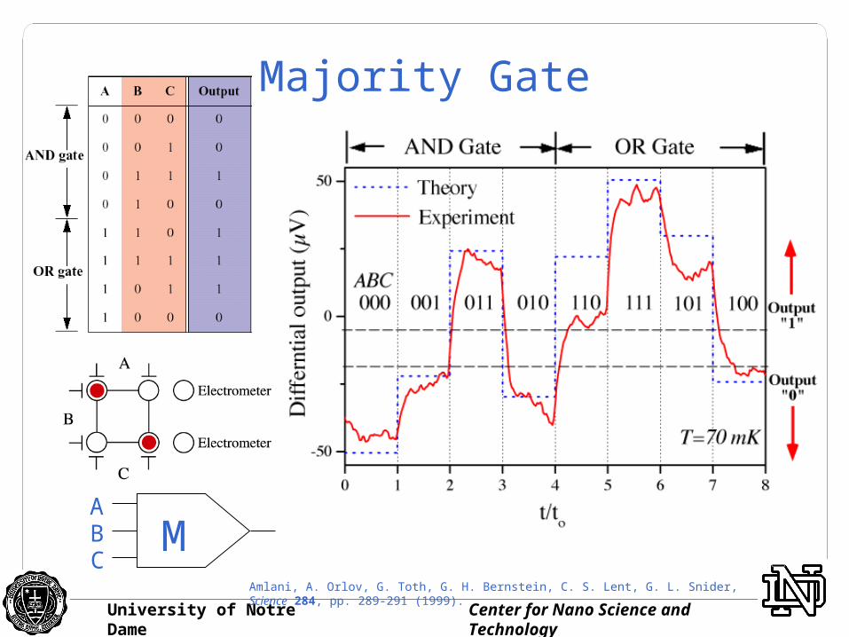
Binary wire
InverterMajority gate
MABC
Programmable 2-input AND or OR gate.
QCA devices
University of Notre Dame Center for Nano Science and Technology
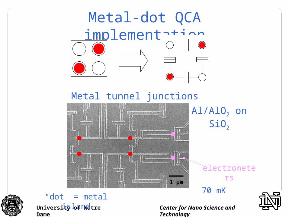
Metal-dot QCA implementation
“dot” = metal island70 mK
electrometers
Al/AlO2 on SiO2
Metal tunnel junctions
1 µm
University of Notre Dame Center for Nano Science and Technology
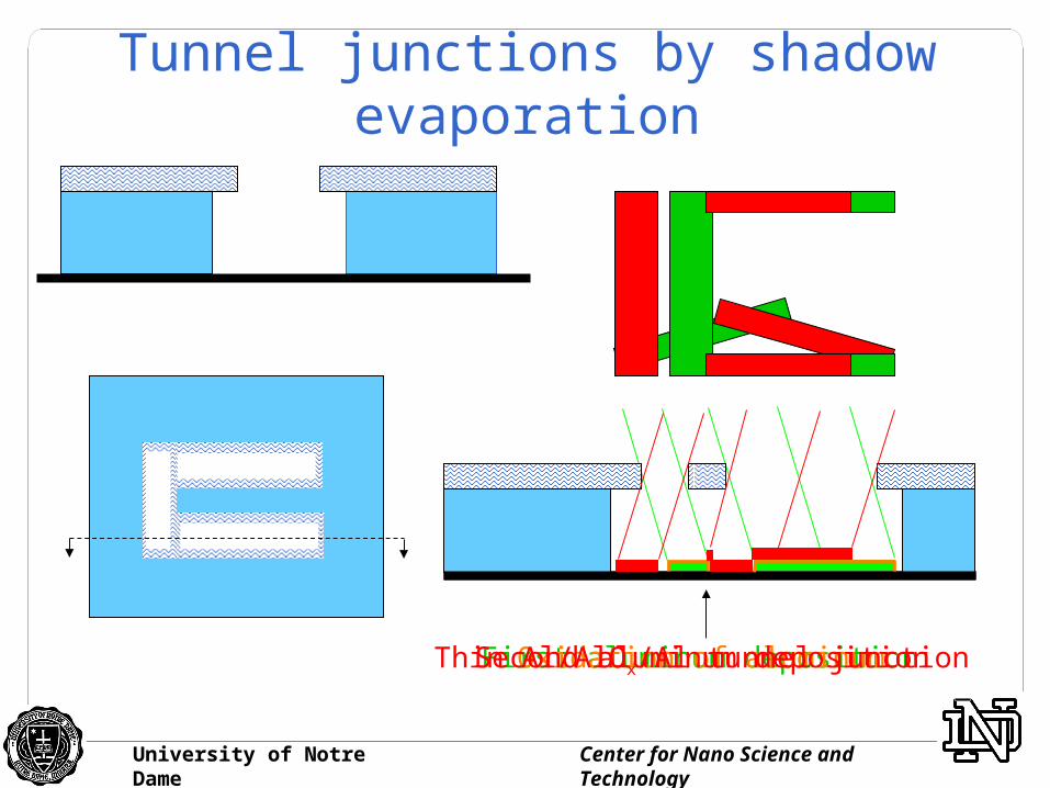
Tunnel junctions by shadow evaporation
First aluminum depositionOxidation of aluminumSecond aluminum depositionThin Al/AlOx/Al tunnel junction
University of Notre Dame Center for Nano Science and Technology
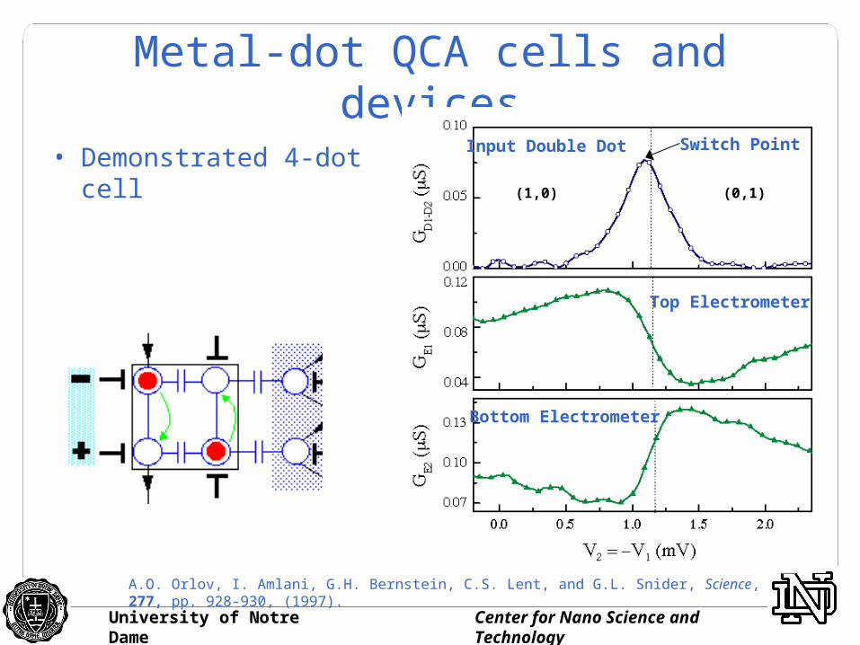
Metal-dot QCA cells and devices
• Demonstrated 4-dot cell
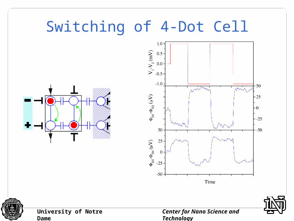
A.O. Orlov, I. Amlani, G.H. Bernstein, C.S. Lent, and G.L. Snider, Science, 277, pp. 928-930, (1997).
Input Double Dot
(1,0) (0,1)
Switch Point
Top Electrometer
Bottom Electrometer
University of Notre Dame Center for Nano Science and Technology
Switching of 4-Dot Cell
University of Notre Dame Center for Nano Science and Technology
Majority Gate
MABC
Amlani, A. Orlov, G. Toth, G. H. Bernstein, C. S. Lent, G. L. Snider, Science 284, pp. 289-291 (1999).
University of Notre Dame Center for Nano Science and Technology
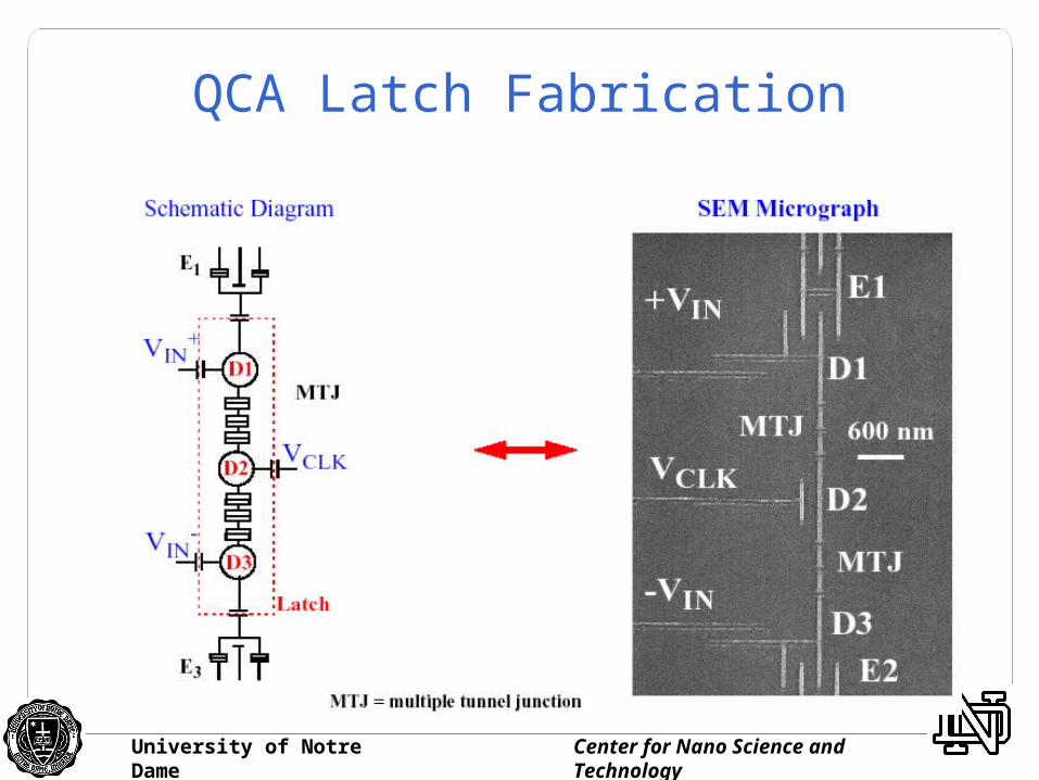
QCA Latch Fabrication
University of Notre Dame Center for Nano Science and Technology
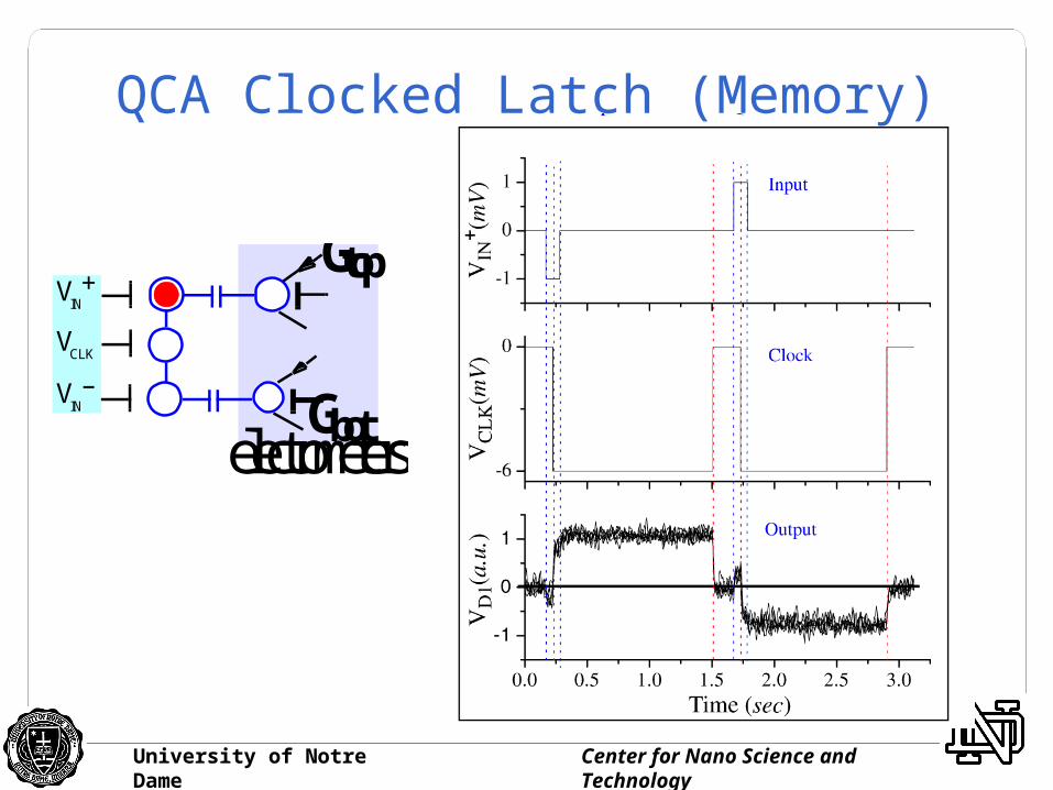
Gtop
Gbotelectrometers
VIN+
VIN–
VCLK
QCA Clocked Latch (Memory)
University of Notre Dame Center for Nano Science and Technology
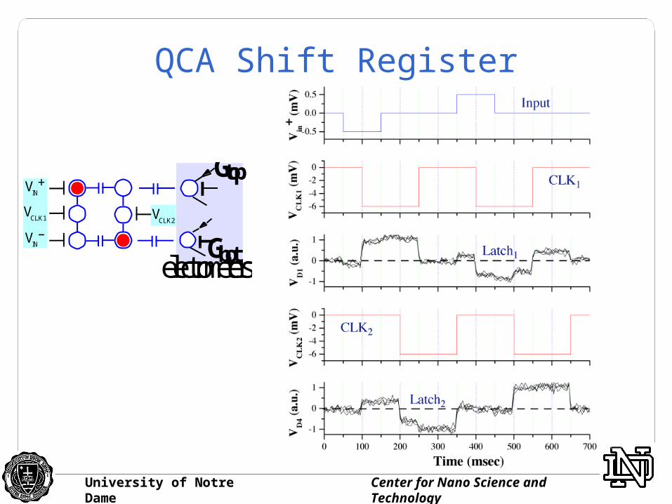
QCA Shift Register
Gtop
Gbotelectrometers
VIN+
VIN–
VCLK1 V
CLK2
University of Notre Dame Center for Nano Science and Technology
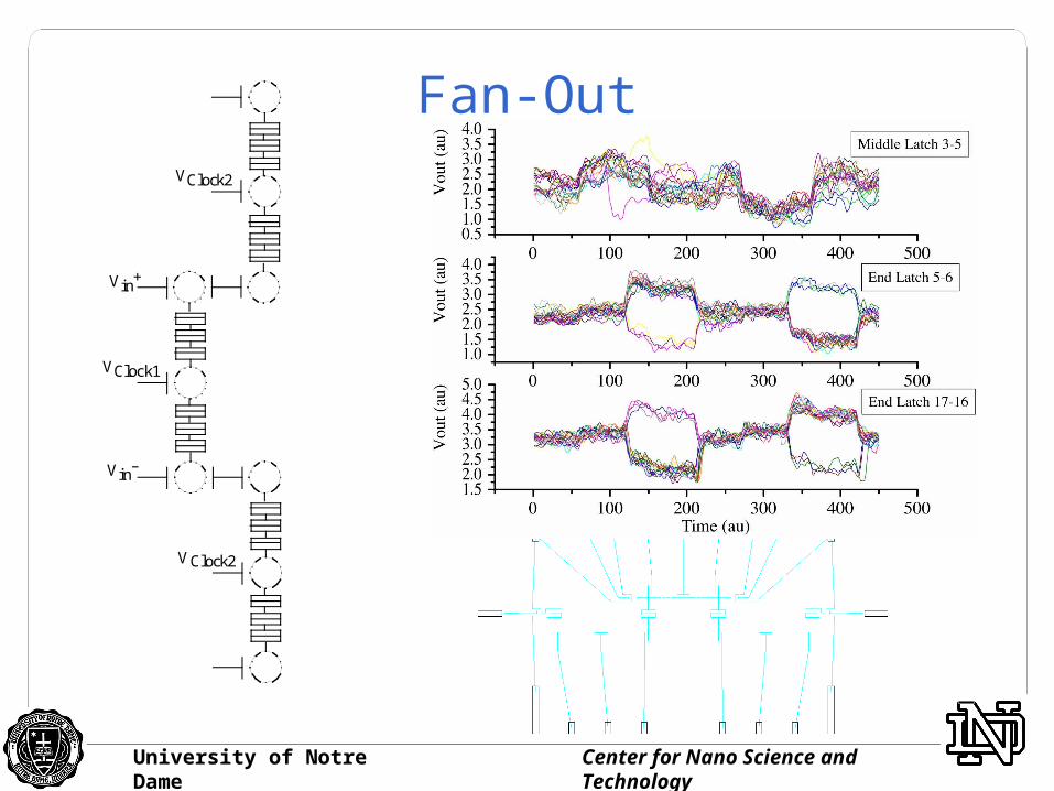
Fan-Out
Vin+
Vin–
VClock1
VClock2
VClock2

University of Notre Dame Center for Nano Science and Technology
From metal-dot to molecular QCA
“dot” = metal island70 mK
Mixed valence compounds
“dot” = redox center
Metal-dot QCA established proof-of-principle.but …low T, fabrication variations
Molecular QCA: room temp, synthetic consistency
room temperature+
Metal tunnel junctions
University of Notre Dame Center for Nano Science and Technology
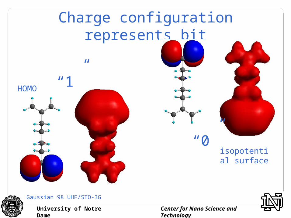
Charge configuration represents bit
“1”
isopotential surface
“0”
Gaussian 98 UHF/STO-3G
HOMO

University of Notre Dame Center for Nano Science and Technology
Double molecule
Considered as a single cell, bit is represented by quadrupole moment.
Alternatively: consider it a dipole driving another dipole.

University of Notre Dame Center for Nano Science and Technology
“0”
HOMO Isopotential (+)
“1”
Double molecule
University of Notre Dame Center for Nano Science and Technology
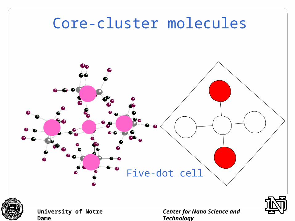
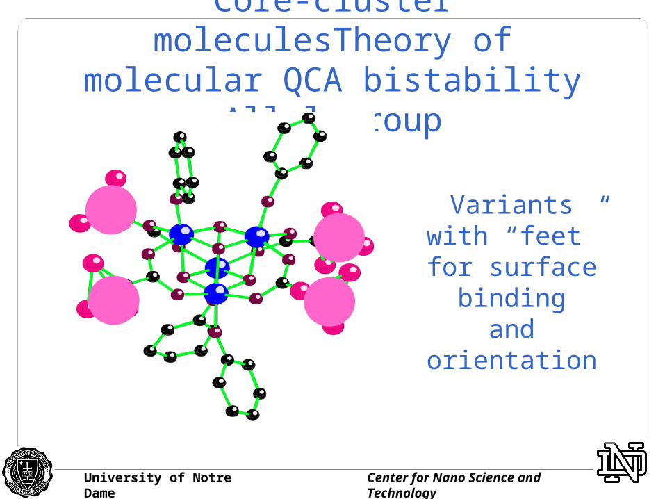
Core-cluster molecules
Five-dot cell
University of Notre Dame Center for Nano Science and Technology
Core-cluster moleculesTheory of molecular QCA bistability Allyl group
Variants with
“feet” for surface bindingand orientation

University of Notre Dame Center for Nano Science and Technology
Electron Switching in QCAMetal Dots
Measure conductance
Molecular Dots
Measure capacitance
C
Voltage
University of Notre Dame Center for Nano Science and Technology
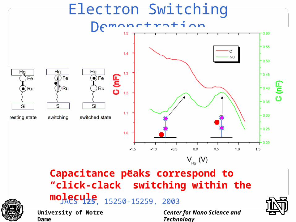
Electron Switching Demonstration
Capacitance peaks correspond to “click-clack” switching within the molecule
JACS 125, 15250-15259, 2003

University of Notre Dame Center for Nano Science and Technology
Clocked molecular QCA
University of Notre Dame Center for Nano Science and Technology
Summary
• QCA may offer a promising paradigm for nanoelectronics– binary digits represented by charge configuration – beyond transistors– general-purpose computing– enormous functional densities– solves power issues: gain and dissipation– Scalable to molecular dimensions
• Single electron memories represent the ultimate scaling