Embed Size (px)
Citation preview
i
UNIVERSITY OF NAIROBI
FACULTY OF ENGINEERING
DEPARTMENT OF ELECTRICAL AND INFORMATION ENGINEERING
PROJECT: A MICROCONTROLLER BASED WIRELESS E-NOTICE BOARD
PROJECT INDEX: 06
NAME: LUBANGA DENNIS WASIOYA
REG. NO: F17/1353/2010
SUPERVISOR: PROF. ELIJAH MWANGI
EXAMINER: MR. C. OMBURA
A project report submitted to the Department of Electrical and Information Engineering in
partial fulfillment of the requirements for the award of the Degree of Bachelor of Science
in Electrical and Electronic Engineering of the University of Nairobi
Submitted on: 24TH
APRIL 2015
i
DECLARATION OF ORIGINALITY
NAME: LUBANGA DENNIS WASIOYA
REGISTRATION NUMBER: F17/1353/2010
COLLEGE: College Of Architecture and Engineering
FACULTY: Engineering
DEPARTMENT: Electrical and Information Engineering
COURSE: Bachelor of Science in Electrical and Electronic
Engineering
PROJECT NAME: A Microcontroller Based Wireless E-Notice Board
1. I understand what plagiarism is and I am aware of the university policy in this regard.
2. I declare that this final year project report is my original work and has not been submitted
elsewhere for examination, award of a degree or publication. Where other people’s work
or my own work has been used, this has properly been acknowledged and referenced in
accordance with the University of Nairobi’s requirements.
3. I have not sought or used the services of any professional agencies to produce this work.
4. I have not allowed, and shall not allow anyone to copy my work with the intention of
passing it off as his/her own work.
5. I understand that any false claim in respect of this work shall result in disciplinary action,
in accordance with University anti-plagiarism policy.
Signature:………………………………………….
Date:………………………………… ………….

ii
DEDICATION
This project is dedicated to my dad, who financially and emotionally supported me through my
entire academic life, and my mom for being there for me always.

iii
ACKNOWLEDGEMENT
First of all, I would like to sincerely express my gratitude to the almighty God who gave me life,
strength and opportunity to get this far in my academic life.
I would also like to thank my supervisor, Prof. Elijah Mwangi, for his insight and valuable
assistance he provided me to make this project work.
I also express my gratitude to the department and especially the electronics laboratory
technicians for the assistance they gave me in completion of my project.
Lastly, I would like to thank my friends and classmates for their educational and any other
related insight they afforded me during the period I was undertaking this project.
iv
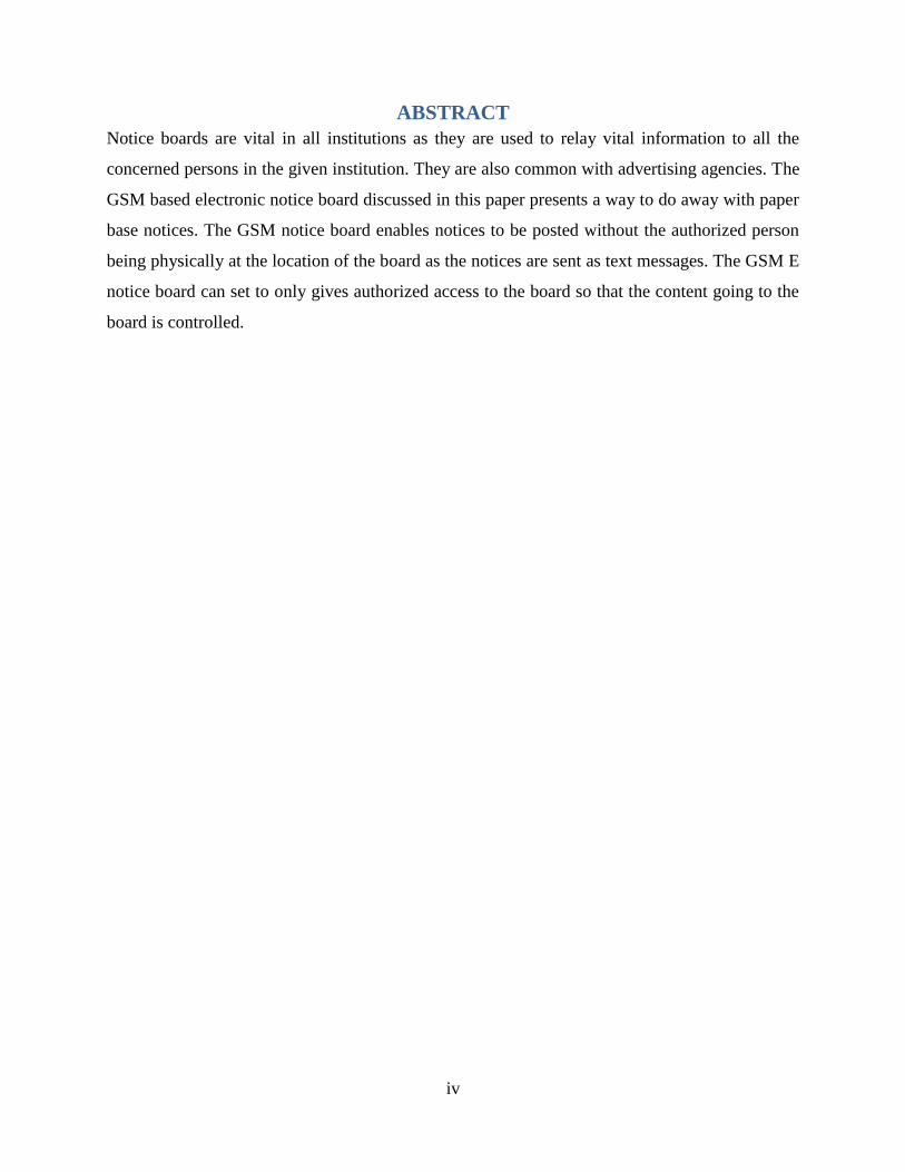
ABSTRACT
Notice boards are vital in all institutions as they are used to relay vital information to all the
concerned persons in the given institution. They are also common with advertising agencies. The
GSM based electronic notice board discussed in this paper presents a way to do away with paper
base notices. The GSM notice board enables notices to be posted without the authorized person
being physically at the location of the board as the notices are sent as text messages. The GSM E
notice board can set to only gives authorized access to the board so that the content going to the
board is controlled.
v
TABLE OF CONTENTS
DECLARATION OF ORIGINALITY ........................................................................................ I
DEDICATION.............................................................................................................................. II
ACKNOWLEDGEMENT .......................................................................................................... III
ABSTRACT ................................................................................................................................. IV
TABLE OF CONTENTS ............................................................................................................ V
ABBREVIATIONS AND ACRONYMS ................................................................................. VII
LIST OF FIGURES ................................................................................................................. VIII
LIST OF TABLES ...................................................................................................................... IX
CHAPTER 1 .................................................................................................................................. 1
INTRODUCTION......................................................................................................................... 1
1.1 BACKGROUND ........................................................................................................................ 1
1.2 PROBLEM STATEMENT ........................................................................................................... 1
1.3 OBJECTIVES ........................................................................................................................... 1
1.4 SCOPE OF WORK .................................................................................................................... 2
1.5 ORGANISATION OF THE PROJECT ............................................................................................ 2
CHAPTER 2 .................................................................................................................................. 3
LITERATURE REVIEW ............................................................................................................ 3
2.1 THE MICROCONTROLLER ....................................................................................................... 3
2.1.1 Classification of microcontrollers .................................................................................. 3
2.1.2 Applications of Microcontrollers ................................................................................... 6
2.1.3 The PIC 16F690 ............................................................................................................. 6
2.2 GSM MODEM ...................................................................................................................... 9
2.3 DISPLAY UNIT ...................................................................................................................... 10
2.3.1 Classification of LCD’s ............................................................................................... 11
2.4 POWER SUPPLY .................................................................................................................... 12
2.5 PROGRAMMING LANGUAGE AND SOFTWARE ....................................................................... 12
2.5.1 Programming Language ............................................................................................... 12
2.5.2 Tools and Computer Software ..................................................................................... 13
CHAPTER 3 ................................................................................................................................ 15
DESIGN AND IMPLEMENTATION ...................................................................................... 15
3.1 SOFTWARE DESIGN .............................................................................................................. 15
3.1.1 The Microcontroller Unit ............................................................................................. 16
3.1.2 LCD Screen .................................................................................................................. 17
3.1.4 Computer Software Used ............................................................................................. 21
vi
3.2 HARDWARE IMPLEMENTATION ............................................................................................ 22
3.2.1 LCD Connections......................................................................................................... 22
3.2.2 GSM connections ......................................................................................................... 23
3.2.3 PIC connections ........................................................................................................... 24
3.2.4 The Power Supply Unit ................................................................................................ 25
CHAPTER 4 ................................................................................................................................ 26
RESULTS AND ANALYSIS ..................................................................................................... 26
4.1 STARTUP DISPLAY ............................................................................................................... 26
4.2 GSM MESSAGE DISPLAY ..................................................................................................... 27
CHAPTER 5 ................................................................................................................................ 28
CONCLUSION AND RECOMMENDATIONS ...................................................................... 28
5.1 CONCLUSIONS ...................................................................................................................... 28
5.2 REALIZATION ON LARGER SCREEN ....................................................................................... 28
5.3 RECOMMENDATIONS ............................................................................................................ 29
BIBLIOGRAPHY ....................................................................................................................... 31
APPENDIX .................................................................................................................................. 33
A. MICROCONTROLLER CODE ................................................................................................. 33
B. PIC16F690 INTERNAL ARCHITECTURE .............................................................................. 41
C. CIRCUIT DIAGRAM ................................................................................................................ 42
D. COST OF MATERIALS ............................................................................................................. 43
vii
ABBREVIATIONS AND ACRONYMS
GSM Global System of Mobile
SIM Subscriber Identification Module
PIC Peripheral interface Control
LCD Liquid Crystal Display
LED Light Emitting Diode
TFT Thin Film Transistor
RX receiver
TX Transmitter
GND Ground
ALU Arithmetic and Logic Unit
CISC Complex Instruction Set Computing
RISC Reduced Instruction Set Computing
PC Personal Computer
IDE Integrated development Environment
ASCII American Standard Code for Information Interchange
ETSI European Telecommunications standards Institute
2G Second Generation
EEPROM Electrically Erasable Programmable Read Only Memory
ROM Read only Memory
ISR Interrupt Service Routine
USART Universal Synchronous Asynchronous Receiver Transmitter
viii
LIST OF FIGURES
Figure 2. 1 Types of Microcontrollers ............................................................................................ 3
Figure 2. 2 Transmitting data using USART module [3] ............................................................... 8
Figure 2. 3 The GSM MODEM .................................................................................................... 10
Figure 2. 4 Internal structure of the LCD screen .......................................................................... 10
Figure 2. 5 A 20 by 4 LCD screen ................................................................................................ 12
Figure 2. 6 Pickit 3 ........................................................................................................................ 14
Figure 3. 1 Software design flowchart .......................................................................................... 15
Figure 3. 2 The STATUS register [9] ........................................................................................... 16
Figure 3. 3The OSCCON register [9] ........................................................................................... 19
Figure 3. 4 The INTCON Register [9] .......................................................................................... 20
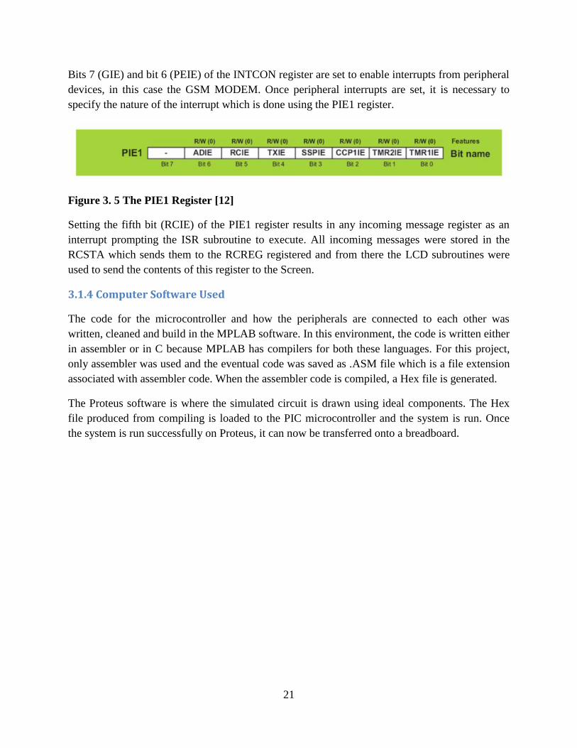
Figure 3. 5 The PIE1 Register [9] ................................................................................................. 21
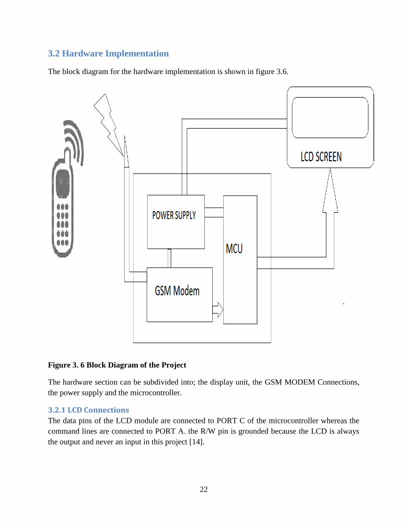
Figure 3. 6 Block Diagram of the Project ..................................................................................... 22
Figure 3. 7 Level Shifter Circuit [12] ........................................................................................... 24
Figure 3. 8 Pin Diagram of the Microcontroller [2] ...................................................................... 24
Figure 3. 9 Voltage Stabilizer Circuit [6] ..................................................................................... 25
Figure 4. 1 Proteus Simulation...................................................................................................... 26
Figure 4. 2 Practical Result ........................................................................................................... 26
Appendix Figure 1. 1 Internal Architecture of PIC16F690 [3] .................................................... 41
Appendix Figure 1. 2 Proteus Circuit Diagram ............................................................................ 41
ix
LIST OF TABLES
Table 3. 1: Bank Selection ............................................................................................................ 17
Table 3. 2: LCD Instructions ........................................................................................................ 18
Table 3. 3: Internal Clock setting .................................................................................................. 19
Table 3. 4: Baud Rate setting [12] ................................................................................................ 20
Table 3. 5: LCD pin Connections ................................................................................................. 23

x
1
CHAPTER 1
INTRODUCTION
1.1 Background
Microcontrollers have become an integral part of modern systems as they provide the ability to
create stand alone systems which have revolutionize the technological world. The ability to
program microcontrollers to perform a given task under a certain circumstance and react
differently in another situation has made our work easier in many ways. In order to create any
system, a microcontroller is interfaced with several peripheral devices depending on what the
system designer wants to create. For example, to create a notice board as in this project, a display
unit and a GSM MODEM are connected to the microcontroller. The GSM MODEM is
responsible for the reception of the notices and sends the information to the microcontroller
which in turn sends the message to the display unit [1].
This is just one example of the systems that can be actualized by connecting a microcontroller to
some other devices. There are many systems that can be made using microcontrollers. This
project discusses the making of a wireless notice board and explains how it can be implemented
on a larger and economically viable way.
1.2 Problem Statement
A notice board is an important item in any institution as it is used to pass any information to
people in the institution. They are also very important in the advertising field as companies
market their products and services on these boards. All along, the notice boards have been
“physical” with the notices printed on a piece of paper and posted on the boards. The wireless E
notice board provides the unique opportunity of posting notices remotely from any location in
the world provided there area has GSM network coverage. However, notice boards can distract
motorists on the roads and lead to accidents. It is therefore important to regulate the information
one puts on these boards so as to ensure they are less distractive.
1.3 Objectives
The objectives of this project is to design a GSM E-Notice board based on the PIC
microcontroller that will have the following functionalities;
Receive a text message sent through the GSM network
Display the message on a LCD screen
Discuss how the project can be realized using the more economically practical TFT LCD
and LED screens
2
1.4 Scope of Work
The project covers the following areas;
Using a PIC microcontroller to display text on an LCD screen
Connecting a GSM MODEM to a microcontroller and receive text messages from a
mobile phone through the GSM Network
If the received text is from an authorized source, display the text on the LCD screen, if
not authorized, discard the text message
The other functionalities of the GSM MODEM such as receiving calls and checking the signal
strength of the GSM network are not within the scope of this project
1.5 Organisation of the Project
The project is organized into five chapters as follows: the introduction, the literature review,
design and implementation, results then the conclusions and recommendations. After the
chapters there are the references and lastly the appendix.
The introduction to the project discusses the background of the project, problem statement,
objectives and the project scope.
The literature review section is where the various components of the project are discussed. These
components include the GSM MODEM, the microcontroller, the power supply and also the
programming language and the software used.
The design and implementation chapter focuses on the software and hardware implementation of
the project. The software part discusses how the modules are interfaced in the program code and
the hardware design focuses on the physical creation of the wireless E-Notice board system.
The fourth chapter is where the results of the project are presented and their analysis given. The
results of the project are divided into; simulated and practical. The simulated results are seen
from the software in the PC and the practical results are seen on the Breadboard from actual
circuitry.
The fifth chapter concludes the findings of the entire project and recommends what should be
done for further works in line with that project.
References of the project are given after the fifth chapter. The appendix has the MCU code used,
the circuit diagram, important figures and the breakdown of the project cost.
3
CHAPTER 2
LITERATURE REVIEW
This chapter discusses the various components and aspects that have been used in this project.
These are the microcontroller, the LCD screen, the GSM/GPRS MODEM, the power supply,
software and other tools used.
2.1 The Microcontroller
By definition, a microcontroller is simply a computer on a chip. To be able to produce any
system, like a GSM E-Notice board, several peripheral devices are to be interfaced with the
microcontroller and a code is programmed into the microcontroller to enable the peripherals to
work in a certain way so that the system is complete [2]. The microcontrollers are of different
types and they are classified in different ways.
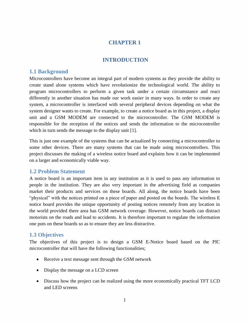
2.1.1 Classification of microcontrollers
Microcontrollers can be classified into many types based of various aspects some of them being;
bus width, instruction set, memory architecture, instruction set and family. Here we shall look at
all these classification aspects with special reference to the PIC 16F690. Figure 2.1 shows one
way of classifying microcontrollers.
Figure 2. 1 Types of Microcontrollers [1]
4
2.1.1.1 Memory Architecture
Architecture is the conceptual design and operational structure of the microcontroller. There are
two main architectural designs which are considered to classify any microcontroller, the Von
Neumann and the Harvard architectures. The two architectural designs differ in the way data and
programs are accessed and stored.
2.1.1.1.1 Harvard Architecture
In this memory architecture, the program memory is completely separated from the data
memory. All PIC microcontrollers have the Harvard architecture. With the separate physical
memories, each memory has its special dedicated bus used for instruction and data flow. This
allows faster execution of commands and parallel flow of data is possible [2].
2.1.1.1.2 Von Neumann Architecture
In this design, the controller can either read an instruction or write one but not read and write at
the same time as the two processes use a single bus for instruction and data transfer. The
advantage of the von Neumann architecture is that it can handle both a program with very large
program memory requirements but little data space or one with very little program memory
requirement with very large data amount without any problem. It is also able to optimize
memory for both cases.
The architecture, however, has many disadvantages thus making it not very common among the
microcontrollers. First, since the memory is the same for the entire chip, if you happen to
misplace the place holder of the instruction to be executed next your computer may “hang”.
Also, some program data may be moved to the next memory location if it doesn’t fit in the
desired destination. This next location can contain data from another program and hence this will
intentionally overrun the data memory with program instructions [2].
2.1.1.2 Bus Width
Classifications according to the width of the internal data bus of the microcontroller lead to the
following types:
2.1.1.2.1 8-bit Microcontroller
A microcontroller is regarded as an 8-bit microcontroller when the ALU performs its operations
on a byte at an instruction. This simply means that the internal bus width is 8-bit long. Examples
of 8-bit microcontrollers are Intel 8051 family and Motorola MC68HC11 family. The
PIC16F690 microcontroller which is used in this project falls under this category.
2.1.1.2.2 16-bit microcontroller
The data bus width of this family of microcontrollers is 16- bit as the names suggest. Examples
of 16-bit microcontrollers are Intel 8096 family and Motorola MC68HC12 and MC68332
families. The capabilities of this microcontroller family are greatly improved as compared to the
earlier family.
5
2.1.1.2.3 32-bit microcontroller
As the name suggest, the internal bus width is 32 bits long. Examples of this family are the Intel
80960 family and Motorola M683xx and Intel/Atmel 251 family Again their capabilities greatly
surpass those of the 16 bit bus width.
2.1.1.3 Instruction Set
Classification made taking into account the instruction sets, results in three distinct types of
microcontrollers i.e. CISC, RISC and SISC.
2.1.1.3.1 CISC
This is an acronym for Complex Instruction Set Computing. This architecture contains a large set
of instruction ranging from very complex to very simple. The disadvantage of the CISC
architecture is that it is easier to compute these complex computations by using short instructions
instead of the complex ones making the CISC architecture inefficient. This led to the
development of the RISC to efficiently work out the inefficiencies of the CISC. Examples of
systems with this architecture are the Intel Pentium processors [2].
2.1.1.3.2 RISC
RISC architecture, which stands for the Reduced Instruction Set computer, uses a small, highly
organized set of instructions as opposed to the complex instructions used by the CISC
architecture. This now the most common architecture used in microcontrollers [2].
Another possible architecture based on the instruction set is the SISC architecture which stands
for Special Instruction Set Computing. This type is not as common as the other two.
2.1.1.4 Memory Devices
This classification yields two types of microcontrollers; embedded memory microcontroller and
external memory microcontroller
2.1.1.4.1 Embedded Memory
This is a microcontroller which has all the functional blocks available on a chip. These functional
blocks are the data memory, I/O ports, Serial communication, counters and timers as well as
interrupts.
2.1.1.4.2 External Memory
Not all the functional blocks are available on the same chip. An example of such is the Intel 8031
where the program memory is not available on the chip and hence an external memory has to be
connected.
6
Microcontrollers can also be classified by the family which is based on the manufacturer of the
microcontroller leading to a number of microcontroller types. The main types are AVR and PIC.
PIC,made by Microchip, is used in this project
2.1.2 Applications of Microcontrollers
Microcontrollers are vital in the building of various devices across the technological divide. The
applications of the microcontroller include:
Light sensing and control devices
Temperature sensing and control devices
Fire detection and safety devices
Industrial instrumentation devices
Process control devices
Voltage, current and power measurement
Measuring revolving objects
Hand held metering systems
Among many other applications
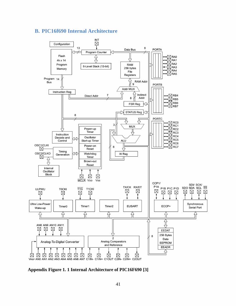
2.1.3 The PIC 16F690
The PIC 16F690 is a 20 pin microcontroller. This PIC belongs to the 16 series 8-bit mid-range
class of PIC microcontrollers with a typical range of interfaces which includes;
Digital input/output
Analog inputs (12 pins)
Multimode timers (3)
Serial ports
An internal clock (4MHz)
The chip has 4K of program memory, 256 bytes of SRAM and another 256 bytes of
EEPROM.The chip can be initialized to provide 18 I/O pins and the other two are for VDD and
VSS. The 18 pins are grouped into three ports, A (6pins), B (4 pins) and C (8 pins) [3].
7
Other important features of the PIC16 F690 that are instrumental in the construction of the E-
Notice board are;
Serial ports (mostly the USART)
Interrupts
EEPROM Data Memory
2.1.3.1 Serial Ports
Serial ports allow the PIC to communicate with a wide range of other devices; in our case we
want the microcontroller to communicate with the LCDs and the GSM MODEM so as to send
messages to the Notice Board. The USART stands for Universal Synchronous/Asynchronous
Receiver/Transmitter. The use of the USART involves sending or receiving an 8-bit or 9-bit
packet of data i.e. a byte of data plus a parity bit where the parity bit is used for error checking
the byte sent. The error checking mechanism works such that if there are an odd number of ones
in the data byte sent or received then the parity bit will be 1 and if the number of 1s is even then
the parity bit will be 0. If there is an error in the sent or received data then the parity bits of the
two will not match and hence the receiver will detect an error [4].
The USART module has two modes of operation i.e. asynchronous operation and synchronous
operation.
In Asynchronous operation, the RX pin of the PIC microcontroller is connected to the TX pin of
the device (in our case the GSM MODEM) and the data is swapped. This connection is referred
to as Full Duplex connection.
In synchronous operation, clock and data lines are shared between a number of devices with the
master device responsible for providing the clock.
In both these modes, the rate at which data is sent by the transmitter should be equal to the rate at
which the receiver expects the same data. This rate is known as the Baud Rate, which for this
project is set at 9600. The baud rate is set using register SPBRG which is located in Bank 1.
In the PIC microcontrollers, the registers responsible for receiving and transmission of data are
the RCSTA (located in Bank 0) and the TXSTA (located in Bank 1). Data read is stored in the
RCREG register (located in Bank 1) whereas data to be transmitted is stored in the TXREG
register also in Bank 1
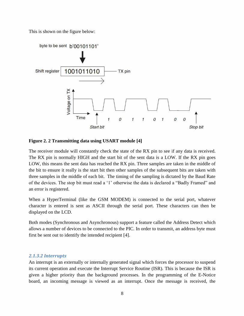
When the USART is to send data (8 OR 9- Bits long) the module adds a start bit (usually a 0) to
the front of the data to be sent and a stop bit (usually a 1) to the end of the data resulting in a 10
or 11-bit long data. This is then moved to the shift register which rotates the bits onto the
transmission pin (TX).
8
This is shown on the figure below:
Figure 2. 2 Transmitting data using USART module [4]
The receiver module will constantly check the state of the RX pin to see if any data is received.
The RX pin is normally HIGH and the start bit of the sent data is a LOW. If the RX pin goes
LOW, this means the sent data has reached the RX pin. Three samples are taken in the middle of
the bit to ensure it really is the start bit then other samples of the subsequent bits are taken with
three samples in the middle of each bit. The timing of the sampling is dictated by the Baud Rate
of the devices. The stop bit must read a ‘1’ otherwise the data is declared a “Badly Framed” and
an error is registered.
When a HyperTerminal (like the GSM MODEM) is connected to the serial port, whatever
character is entered is sent as ASCII through the serial port. These characters can then be
displayed on the LCD.
Both modes (Synchronous and Asynchronous) support a feature called the Address Detect which
allows a number of devices to be connected to the PIC. In order to transmit, an address byte must
first be sent out to identify the intended recipient [4].
2.1.3.2 Interrupts
An interrupt is an externally or internally generated signal which forces the processor to suspend
its current operation and execute the Interrupt Service Routine (ISR). This is because the ISR is
given a higher priority than the background processes. In the programming of the E-Notice
board, an incoming message is viewed as an interrupt. Once the message is received, the
9
processor leaves whatever it was doing, displays the message if it is from an authorized source or
discards the message if the source is not authorized [5].
2.1.3.3 EEPROM Data Memory
The EEPROM is a collection of General Purpose file registers whose contents remain intact even
when power to the microcontroller is cut off. Information that is vital to the functioning of a
system like the passwords and authorized phone numbers are stored in the EEPROM.
The file register EEADR (located in Bank 3) holds the address in the EEPROM which you wish
to read from or writes to while EEDATA file register holds the data you have just read or wish to
write in the EEPROM. The writing process involves the use of registers EECON1 and EECON2,
both of which are located in Bank 3. EECON1 is used to hold setting of the EEPROM whereas
the EECON2 is a special function register used in the EEPROM writing process.
In the creating of the Notice board, it is important that only authorized persons get to display
notices on the board. The EEPROM is important to this function as the programmer gets to give
certain users this opportunity by storing their phone numbers in the EEPROM. As mentioned
earlier the EEPROM memory for the PIC 16F690 is 256 bytes [5].
2.2 GSM MODEM
GSM, acronym for the Global System of Mobile Communication, are standards set by the
European Telecommunications Standard Institute (ETSI) to describe the protocols of the 2G
digital cellular networks used for mobile phones. By the year 2014, the GSM network was the
default mobile communication system in the world with over 90% of the market share for mobile
communication which translates to coverage in 219 countries and territories. Since the GSM
network covers our entire country, a GSM MODEM will be appropriate for use in this project.
The GSM MODEM is a specialized MODEM that accepts a SIM card and operates via
subscription to a mobile operator just like a mobile phone. The SIM card used in the GSM
MODEM is from the wireless carriers such as Safaricom, Airtel or Orange. The GSM MODEM
has the following capabilities when used in a system;
Reading, writing and deleting of messages
Sending of text messages
Monitoring the signal strength
Reading writing and searching entries in the phonebook
The GSM MODEM used in this project is the SIM 900 Mini Wireless Data Transmission
Module GSM/GPRS board kit w/Antenna.
10
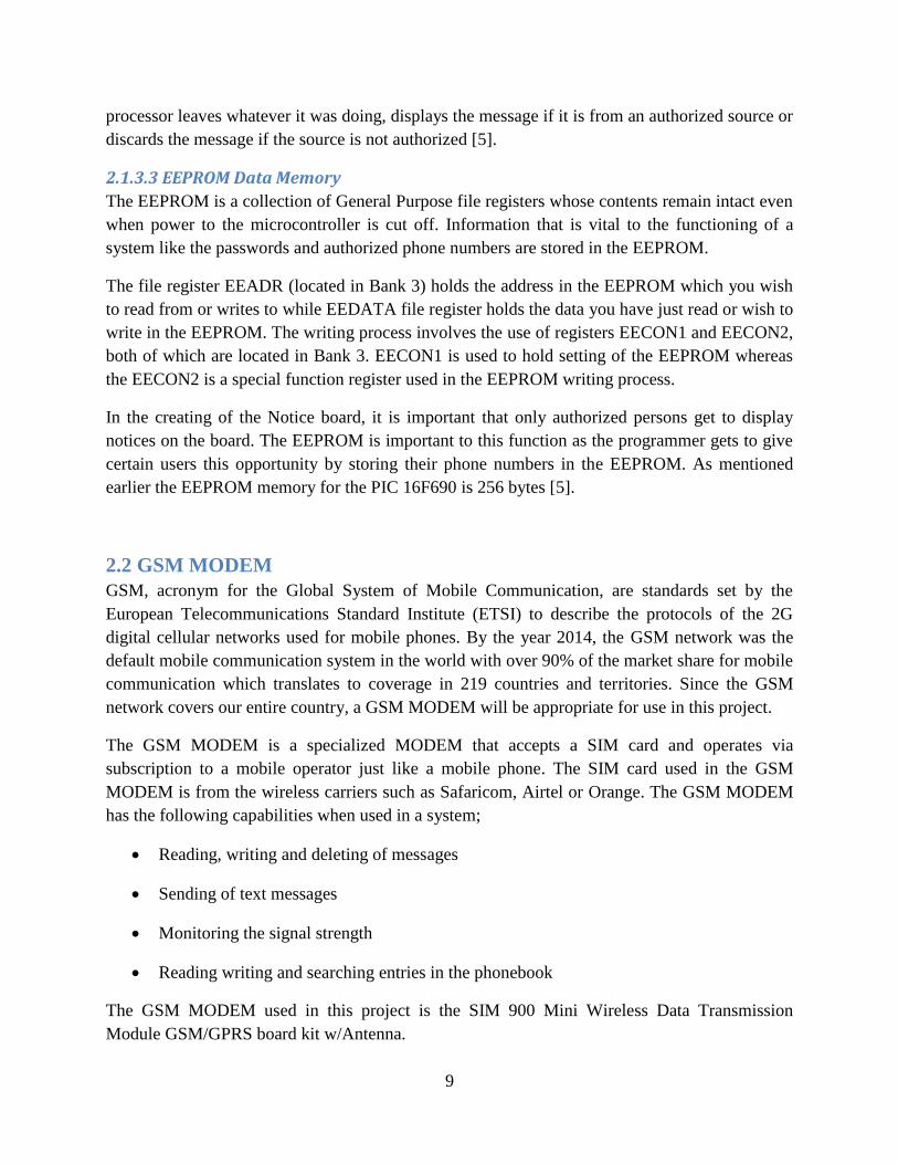
The figure 2.3 below shows the GSM MODEM that will be used in this project
Figure 2. 3 The GSM MODEM [6]
2.3 Display Unit
In this project, the display of the messages/notices is handled by the LCD, an acronym that
stands for Liquid Crystal Display. The LCD screen is an output device which enables the
messages or notice to be displayed for the intended audience to see it. The display on the screen
can be ASCII characters or dot based graphics depending on the message to be displayed.
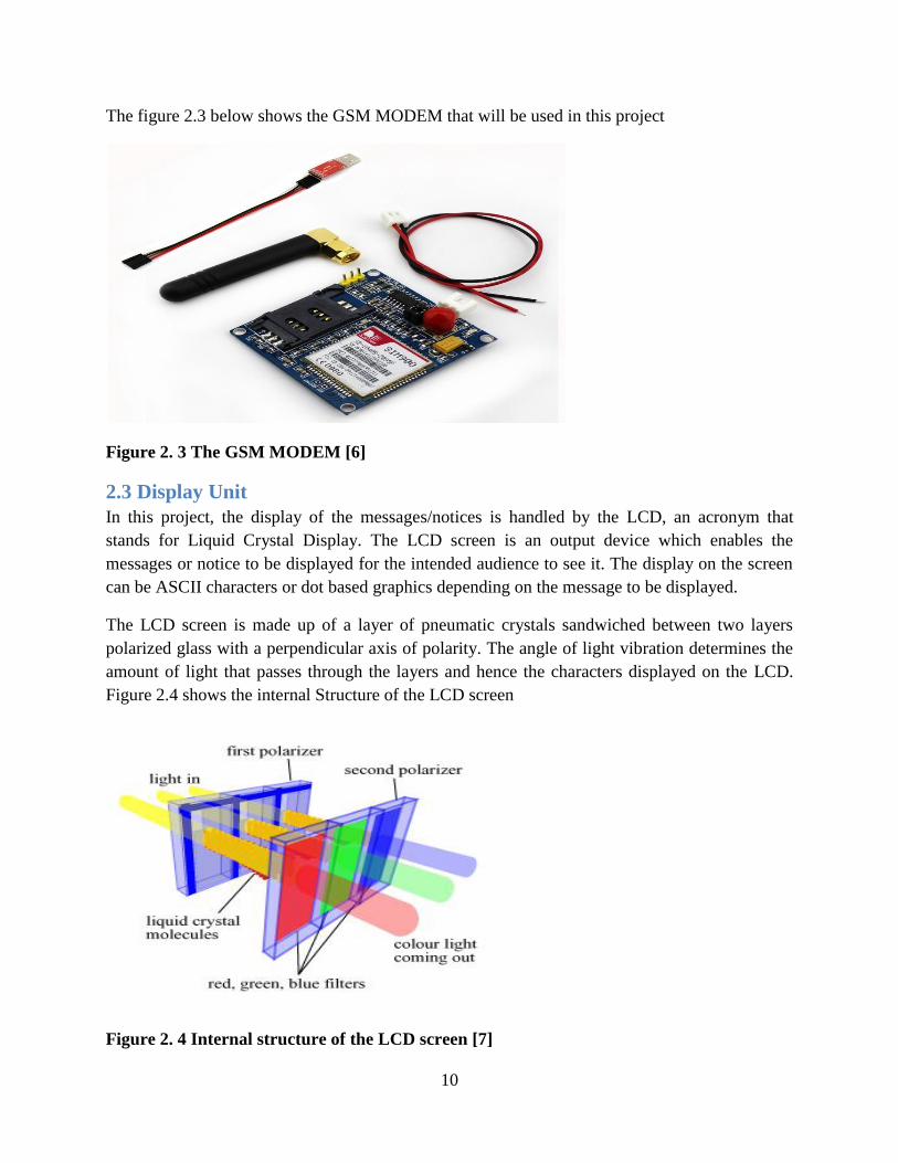
The LCD screen is made up of a layer of pneumatic crystals sandwiched between two layers
polarized glass with a perpendicular axis of polarity. The angle of light vibration determines the
amount of light that passes through the layers and hence the characters displayed on the LCD.
Figure 2.4 shows the internal Structure of the LCD screen
Figure 2. 4 Internal structure of the LCD screen [7]
11
The electric current supplied to the LCD affect the angle of twist of the liquid crystal hence the
amount of light that passes through the LCD. This is how the display of the different characters
is achieved using the LCD screen.
2.3.1 Classification of LCD’s
There are three criteria with which LCDs are classified by with each criterion resulting in several
types of LCDs.
2.3.1.1 According to how they are illuminated
LCDs can be illuminated either from the back, from an external source or from a combination of
the two methods
When the pixels of the LCDs are illuminated from behind the monitor screen and the LCD is
viewed from the front then the LCD is said to be transmissive. Transmissive LCDs are common
in appliances which require high level illumination such as laptop computers and television sets.
When the pixels are illuminated from the front of the screen, the same side as the user is said to
be a reflective LCD. This type of LCD is suitable for low power consumption applications and is
therefore common in digital watches and calculators. This is the type of LCD which is used in
this project.
When the pixels can either be illuminated from the front or from the back of the screen then the
LCD is said to be transflective. The term transflective is used to show that this particular LCD is
a combination of both the transmissive and the reflective LCDs. This LCD works either as a
reflective or a transmissive LCD depending on the ambient lighting available.
2.3.1.2 Colour or Monochrome LCDs
In the color LCDs, each pixel contains cells which are red, green or blue. A pixel can have sub
pixels each of which contain the three colors which are independently controlled and as a result
the LCD is capable of showing millions of colors for each pixel
The monochrome LCD is the most commonly used with microcontrollers
2.3.1.3 According to Display Technology
Basic on this criterion, LCDs are either alphanumeric or dot addressable. There are three
electrode configuration used for this display using the LCD.
The alphanumeric type, which uses a matrix composed of linear segments, is most common in
microcontroller applications. The seven and sixteen segment electrode configurations as shown
below are suitable for small digital devices such as watches and calculators.
The dot addressable type is necessary when there is need to display an entire character or for
graphical display. This type of LCD has more addressable elements hence its more complex that
12
the earlier mentioned LCD. The matrix format LCD display is the most common in
microcontroller circuits.
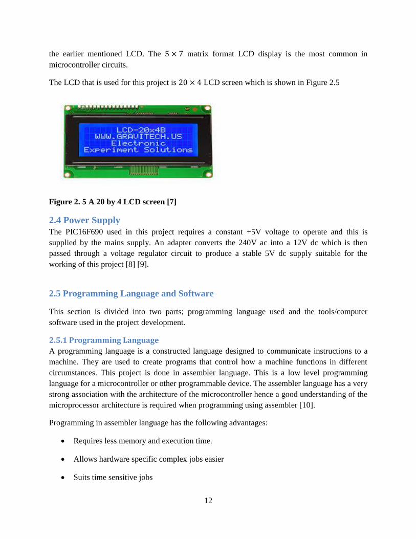
The LCD that is used for this project is LCD screen which is shown in Figure 2.5
Figure 2. 5 A 20 by 4 LCD screen [7]
2.4 Power Supply
The PIC16F690 used in this project requires a constant +5V voltage to operate and this is
supplied by the mains supply. An adapter converts the 240V ac into a 12V dc which is then
passed through a voltage regulator circuit to produce a stable 5V dc supply suitable for the
working of this project [8] [9].
2.5 Programming Language and Software
This section is divided into two parts; programming language used and the tools/computer
software used in the project development.
2.5.1 Programming Language
A programming language is a constructed language designed to communicate instructions to a
machine. They are used to create programs that control how a machine functions in different
circumstances. This project is done in assembler language. This is a low level programming
language for a microcontroller or other programmable device. The assembler language has a very
strong association with the architecture of the microcontroller hence a good understanding of the
microprocessor architecture is required when programming using assembler [10].
Programming in assembler language has the following advantages:
Requires less memory and execution time.
Allows hardware specific complex jobs easier
Suits time sensitive jobs
13
2.5.2 Tools and Computer Software
These are the hardware and computer software used during the project in various sections of
building the prototype and the eventual finished project. The tool used is the Pickit 3 whereas the
software programs used are MPLAB and Proteus.
2.5.2.1 MPLAB
This is software, developed by Microchip, which gives a platform for the writing and debugging
of the assembler language. The MPLAB software is furnished with an IDE which allows the user
to develop software of embedded systems. Software for an embedded system is referred to as
firmware as it cannot be easily changed and requires special equipment i.e. the programmer to
put it on the system it was designed for. The only disadvantage of the MPLAB software is that it
was designed PC. A user on Mac, UNIX or Linux systems cannot use MPLAB. This is however
not a problem to us because the project was done on a PC [12].
2.5.2.2 Proteus
Proteus is simulation software which enables us to see if the code that has been written serves the
intended purpose. The Proteus software enables us to draw the circuit of the particular project
including all the passive and active components required to make the circuit work. The code for
the particular section is input and when the circuit is run, experimental results of the project are
obtained. The only disadvantage of using Proteus is that it assumes all the components are ideal
and hence the experimental results are not necessary the same as the practical ones. This force
the designer to be as close as possible to the experimental results hence a good quality product is
obtained [12].
2.5.2.3 Programmer
Relating to microcontroller technology, the process by which a program is transferred to a chip is
called burning or blowing the chip. A device that burns a program onto a chip is called a
programmer. A programmer contains the following components:
A software package to run on a PC
A cable connecting the PC to the programmer
A programmer device
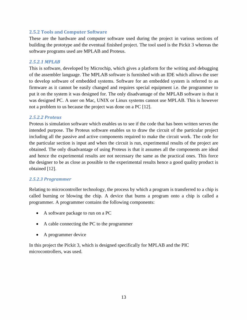
In this project the Pickit 3, which is designed specifically for MPLAB and the PIC
microcontrollers, was used.
14
A photo of the Pickit 3 with its accessories is shown in figure 2.6
Figure 2. 6 Pickit 3 [11]
15
CHAPTER 3
DESIGN AND IMPLEMENTATION
This section discusses how the wireless Electronic Notice board was designed and implemented
using the PIC 16F690. The section is broken down into the:
Software module.
Hardware module.
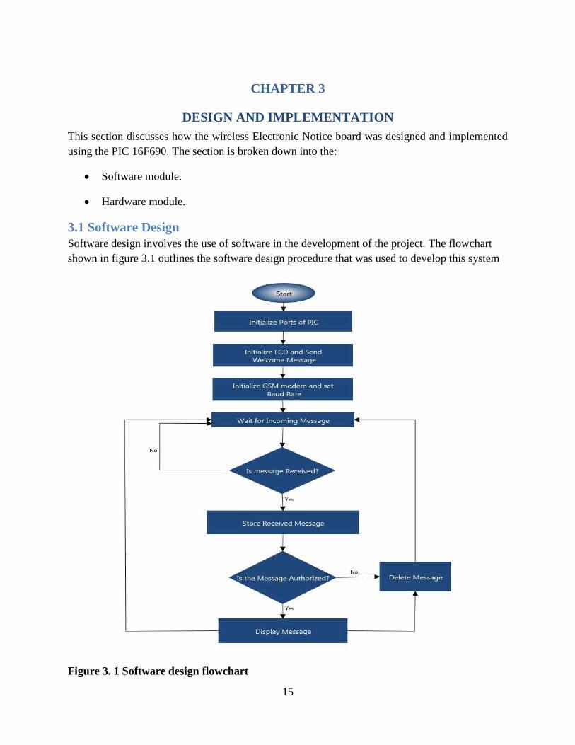
3.1 Software Design
Software design involves the use of software in the development of the project. The flowchart
shown in figure 3.1 outlines the software design procedure that was used to develop this system
Figure 3. 1 Software design flowchart
16
Software design was divided into four parts namely; the Microcontroller Unit, the LCD screen,
the USART functions and the Computer software used.
3.1.1 The Microcontroller Unit
For a microcontroller to function, it has to be connected to peripheral devices which are
connected to the ports of the microcontroller. The first thing to do in PIC programming is the
initialization of the ports and pin function assignment.
Initializing the ports of the PIC microcontroller is done by the use of two Special Function
Registers (SFRs); TRIS and PORT. Each port contain a number of pins and for the PIC 16F690
there are three ports A, B and C which contain 6, 4 and 8 pins respectively. A pin can be set,
becomes an input, or cleared, becomes an output, depending on what you want to connect to the
microcontroller. The block of code below is responsible for the initializing of PORTC which is
where the LCD Screen is connected:
Bcf STATUS, RP0
Clear PORTC
Bsf STATUS, RP0
Clear TRISC
Bcf STATUS, RP0
In the above piece of code, the first line selects the bank where the register PORTC is found i.e.
Bank0. Clearing the port, done with line two, initializes the port. The third line is responsible for
moving to Bank1 where the TRIS register is found, clearing TRIS means all the pins of port are
outputs (the direction of data is to the LCD), and finally the last line moves back to the default
Bank0. Bits 5 and 6 of the status register are responsible for the bank selection as shown in
figure 3.2.
Figure 3. 2 The STATUS register [12]
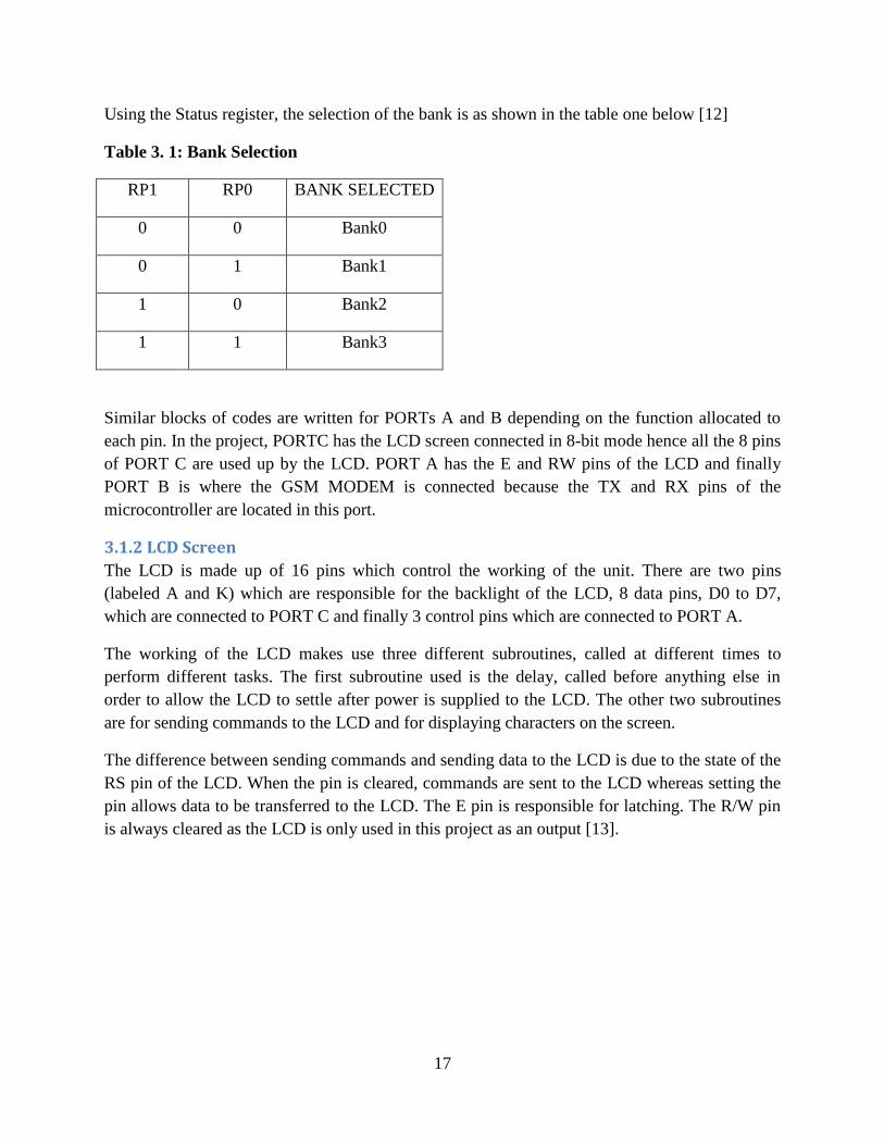
17
Using the Status register, the selection of the bank is as shown in the table one below [12]
Table 3. 1: Bank Selection
RP1 RP0 BANK SELECTED
0 0 Bank0
0 1 Bank1
1 0 Bank2
1 1 Bank3
Similar blocks of codes are written for PORTs A and B depending on the function allocated to
each pin. In the project, PORTC has the LCD screen connected in 8-bit mode hence all the 8 pins
of PORT C are used up by the LCD. PORT A has the E and RW pins of the LCD and finally
PORT B is where the GSM MODEM is connected because the TX and RX pins of the
microcontroller are located in this port.
3.1.2 LCD Screen
The LCD is made up of 16 pins which control the working of the unit. There are two pins
(labeled A and K) which are responsible for the backlight of the LCD, 8 data pins, D0 to D7,
which are connected to PORT C and finally 3 control pins which are connected to PORT A.
The working of the LCD makes use three different subroutines, called at different times to
perform different tasks. The first subroutine used is the delay, called before anything else in
order to allow the LCD to settle after power is supplied to the LCD. The other two subroutines
are for sending commands to the LCD and for displaying characters on the screen.
The difference between sending commands and sending data to the LCD is due to the state of the
RS pin of the LCD. When the pin is cleared, commands are sent to the LCD whereas setting the
pin allows data to be transferred to the LCD. The E pin is responsible for latching. The R/W pin
is always cleared as the LCD is only used in this project as an output [13].
18
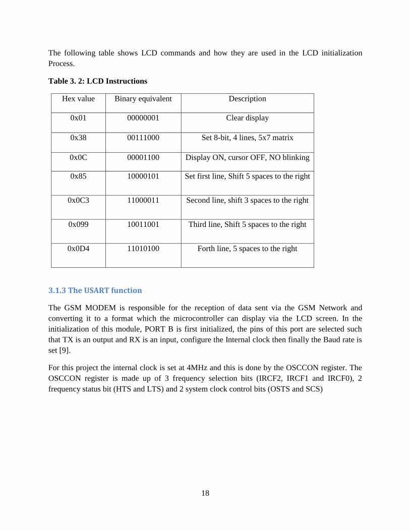
The following table shows LCD commands and how they are used in the LCD initialization
Process.
Table 3. 2: LCD Instructions
Hex value Binary equivalent Description
0x01 00000001 Clear display
0x38 00111000 Set 8-bit, 4 lines, 5x7 matrix
0x0C 00001100 Display ON, cursor OFF, NO blinking
0x85 10000101 Set first line, Shift 5 spaces to the right
0x0C3 11000011 Second line, shift 3 spaces to the right
0x099 10011001 Third line, Shift 5 spaces to the right
0x0D4 11010100 Forth line, 5 spaces to the right
3.1.3 The USART function
The GSM MODEM is responsible for the reception of data sent via the GSM Network and
converting it to a format which the microcontroller can display via the LCD screen. In the
initialization of this module, PORT B is first initialized, the pins of this port are selected such
that TX is an output and RX is an input, configure the Internal clock then finally the Baud rate is
set [9].
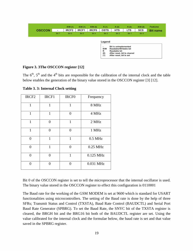
For this project the internal clock is set at 4MHz and this is done by the OSCCON register. The
OSCCON register is made up of 3 frequency selection bits (IRCF2, IRCF1 and IRCF0), 2
frequency status bit (HTS and LTS) and 2 system clock control bits (OSTS and SCS)
19
Figure 3. 3The OSCCON register [12]
The 6th
, 5th
and the 4th
bits are responsible for the calibration of the internal clock and the table
below enables the generation of the binary value stored in the OSCCON register [3] [12].
Table 3. 3: Internal Clock setting
IRCF2 IRCF1 IRCF0 Frequency
1 1 1 8 MHz
1 1 0 4 MHz
1 0 1 2 MHz
1 0 0 1 MHz
0 1 1 0.5 MHz
0 1 0 0.25 MHz
0 0 1 0.125 MHz
0 0 0 0.031 MHz
Bit 0 of the OSCCON register is set to tell the microprocessor that the internal oscillator is used.
The binary value stored in the OSCCON register to effect this configuration is 0110001
The Baud rate for the working of the GSM MODEM is set at 9600 which is standard for USART
functionalities using microcontrollers. The setting of the Baud rate is done by the help of three
SFRs; Transmit Status and Control (TXSTA), Baud Rate Control (BAUDCTL) and Serial Port
Baud Rate Generator (SPBRG). To set the Baud Rate, the SNYC bit of the TXSTA register is
cleared, the BRGH bit and the BRG16 bit both of the BAUDCTL register are set. Using the
value calibrated for the internal clock and the formulae below, the baud rate is set and that value
saved in the SPBRG register.
20
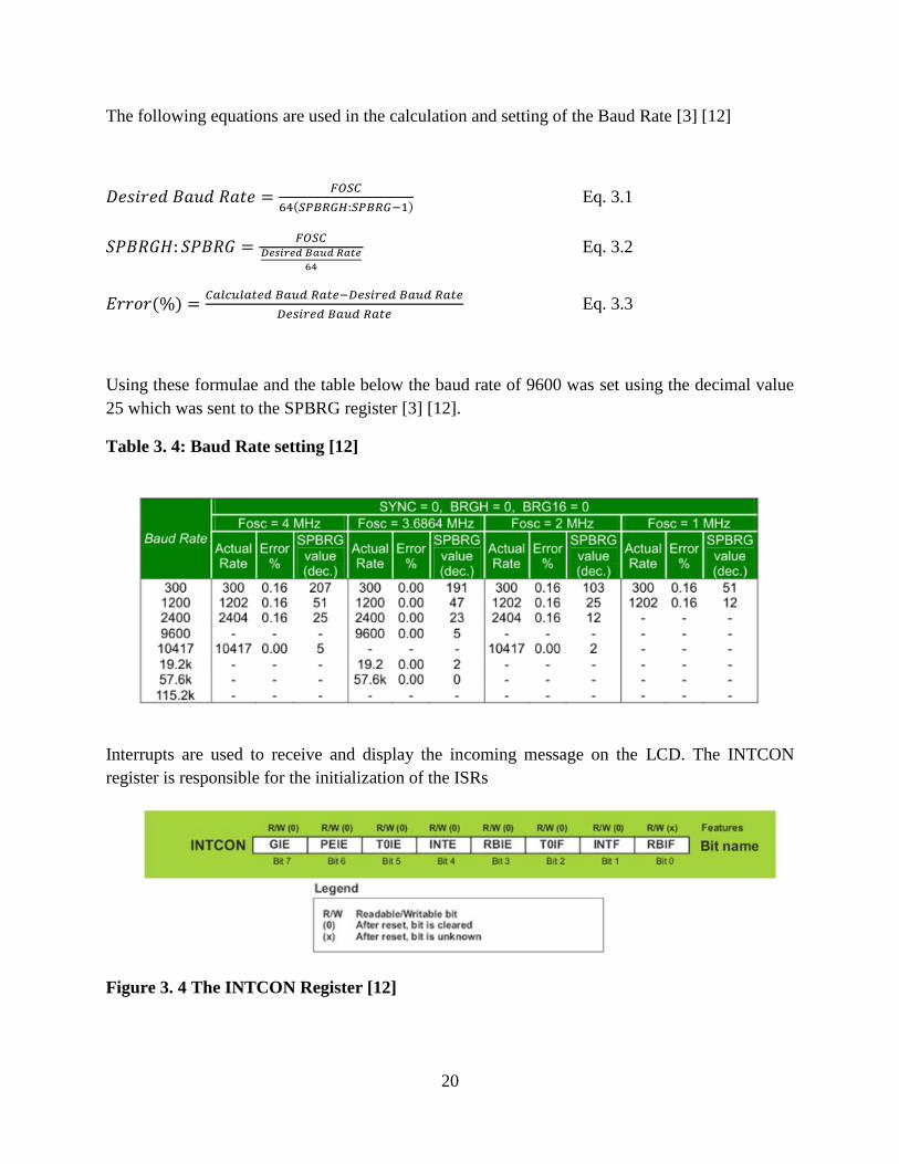
The following equations are used in the calculation and setting of the Baud Rate [3] [12]
Eq. 3.1
Eq. 3.2
Eq. 3.3
Using these formulae and the table below the baud rate of 9600 was set using the decimal value
25 which was sent to the SPBRG register [3] [12].
Table 3. 4: Baud Rate setting [12]
Interrupts are used to receive and display the incoming message on the LCD. The INTCON
register is responsible for the initialization of the ISRs
Figure 3. 4 The INTCON Register [12]
21
Bits 7 (GIE) and bit 6 (PEIE) of the INTCON register are set to enable interrupts from peripheral
devices, in this case the GSM MODEM. Once peripheral interrupts are set, it is necessary to
specify the nature of the interrupt which is done using the PIE1 register.
Figure 3. 5 The PIE1 Register [12]
Setting the fifth bit (RCIE) of the PIE1 register results in any incoming message register as an
interrupt prompting the ISR subroutine to execute. All incoming messages were stored in the
RCSTA which sends them to the RCREG registered and from there the LCD subroutines were
used to send the contents of this register to the Screen.
3.1.4 Computer Software Used
The code for the microcontroller and how the peripherals are connected to each other was
written, cleaned and build in the MPLAB software. In this environment, the code is written either
in assembler or in C because MPLAB has compilers for both these languages. For this project,
only assembler was used and the eventual code was saved as .ASM file which is a file extension
associated with assembler code. When the assembler code is compiled, a Hex file is generated.
The Proteus software is where the simulated circuit is drawn using ideal components. The Hex
file produced from compiling is loaded to the PIC microcontroller and the system is run. Once
the system is run successfully on Proteus, it can now be transferred onto a breadboard.
22
3.2 Hardware Implementation
The block diagram for the hardware implementation is shown in figure 3.6.
Figure 3. 6 Block Diagram of the Project
The hardware section can be subdivided into; the display unit, the GSM MODEM Connections,
the power supply and the microcontroller.
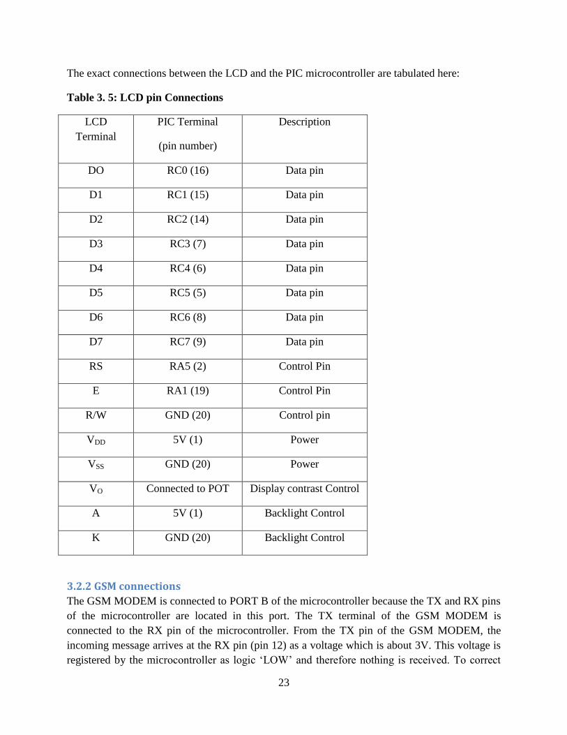
3.2.1 LCD Connections
The data pins of the LCD module are connected to PORT C of the microcontroller whereas the
command lines are connected to PORT A. the R/W pin is grounded because the LCD is always
the output and never an input in this project [14].
23
The exact connections between the LCD and the PIC microcontroller are tabulated here:
Table 3. 5: LCD pin Connections
LCD
Terminal
PIC Terminal
(pin number)
Description
DO RC0 (16) Data pin
D1 RC1 (15) Data pin
D2 RC2 (14) Data pin
D3 RC3 (7) Data pin
D4 RC4 (6) Data pin
D5 RC5 (5) Data pin
D6 RC6 (8) Data pin
D7 RC7 (9) Data pin
RS RA5 (2) Control Pin
E RA1 (19) Control Pin
R/W GND (20) Control pin
VDD 5V (1) Power
VSS GND (20) Power
VO Connected to POT Display contrast Control
A 5V (1) Backlight Control
K GND (20) Backlight Control
3.2.2 GSM connections
The GSM MODEM is connected to PORT B of the microcontroller because the TX and RX pins
of the microcontroller are located in this port. The TX terminal of the GSM MODEM is
connected to the RX pin of the microcontroller. From the TX pin of the GSM MODEM, the
incoming message arrives at the RX pin (pin 12) as a voltage which is about 3V. This voltage is
registered by the microcontroller as logic ‘LOW’ and therefore nothing is received. To correct
24
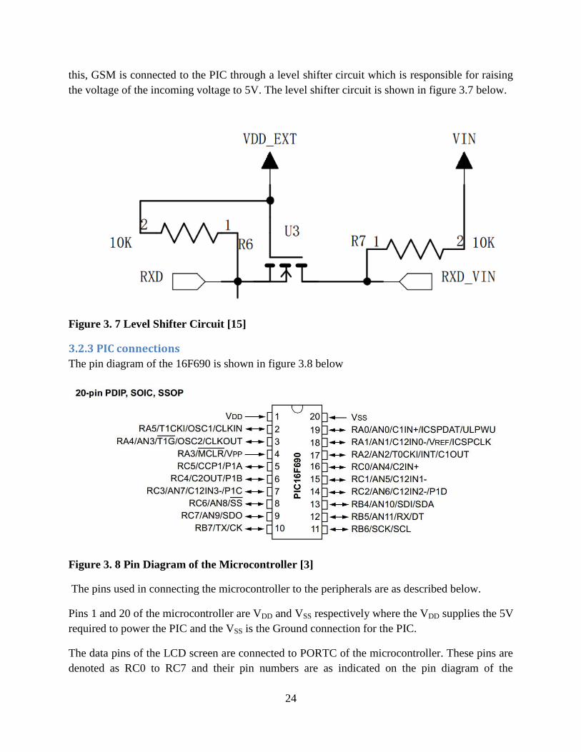
this, GSM is connected to the PIC through a level shifter circuit which is responsible for raising
the voltage of the incoming voltage to 5V. The level shifter circuit is shown in figure 3.7 below.
Figure 3. 7 Level Shifter Circuit [15]
3.2.3 PIC connections
The pin diagram of the 16F690 is shown in figure 3.8 below
Figure 3. 8 Pin Diagram of the Microcontroller [3]
The pins used in connecting the microcontroller to the peripherals are as described below.
Pins 1 and 20 of the microcontroller are VDD and VSS respectively where the VDD supplies the 5V
required to power the PIC and the VSS is the Ground connection for the PIC.
The data pins of the LCD screen are connected to PORTC of the microcontroller. These pins are
denoted as RC0 to RC7 and their pin numbers are as indicated on the pin diagram of the
25
PIC16F690 shown in figure 3.8. The control pins of the LCD are connected on PORTA of the
microcontroller with E terminal of the LCD connected to pin 18 of the PIC and the RS terminal
connected to pin 2 of the PIC. The R/W terminal of the LCD is grounded because we are always
writing to the LCD and never reading from the screen. The LCD receives its power from the VDD
and the VSS terminals which are connected to pins 1 and 20 respectively.
The GSM MODEM is connected to PORTB of the PIC microcontroller. The microcontroller is
receiving from the GSM MODEM and as a result the TX pin of the MODEM is connected to the
RX pin of the PIC (pin 12).
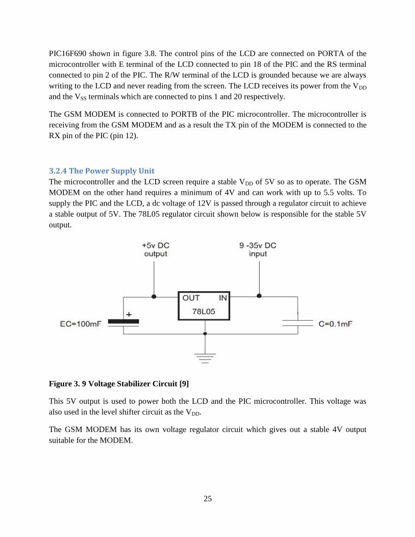
3.2.4 The Power Supply Unit
The microcontroller and the LCD screen require a stable VDD of 5V so as to operate. The GSM
MODEM on the other hand requires a minimum of 4V and can work with up to 5.5 volts. To
supply the PIC and the LCD, a dc voltage of 12V is passed through a regulator circuit to achieve
a stable output of 5V. The 78L05 regulator circuit shown below is responsible for the stable 5V
output.
Figure 3. 9 Voltage Stabilizer Circuit [9]
This 5V output is used to power both the LCD and the PIC microcontroller. This voltage was
also used in the level shifter circuit as the VDD.
The GSM MODEM has its own voltage regulator circuit which gives out a stable 4V output
suitable for the MODEM.
26
CHAPTER 4
RESULTS AND ANALYSIS
This chapter shows the results of the projects and analysis of the results is also presented. This
section takes a look at the simulated and practical results of the project.
This chapter is divided into three sections; Startup display, GSM general message display and
authorized message display.
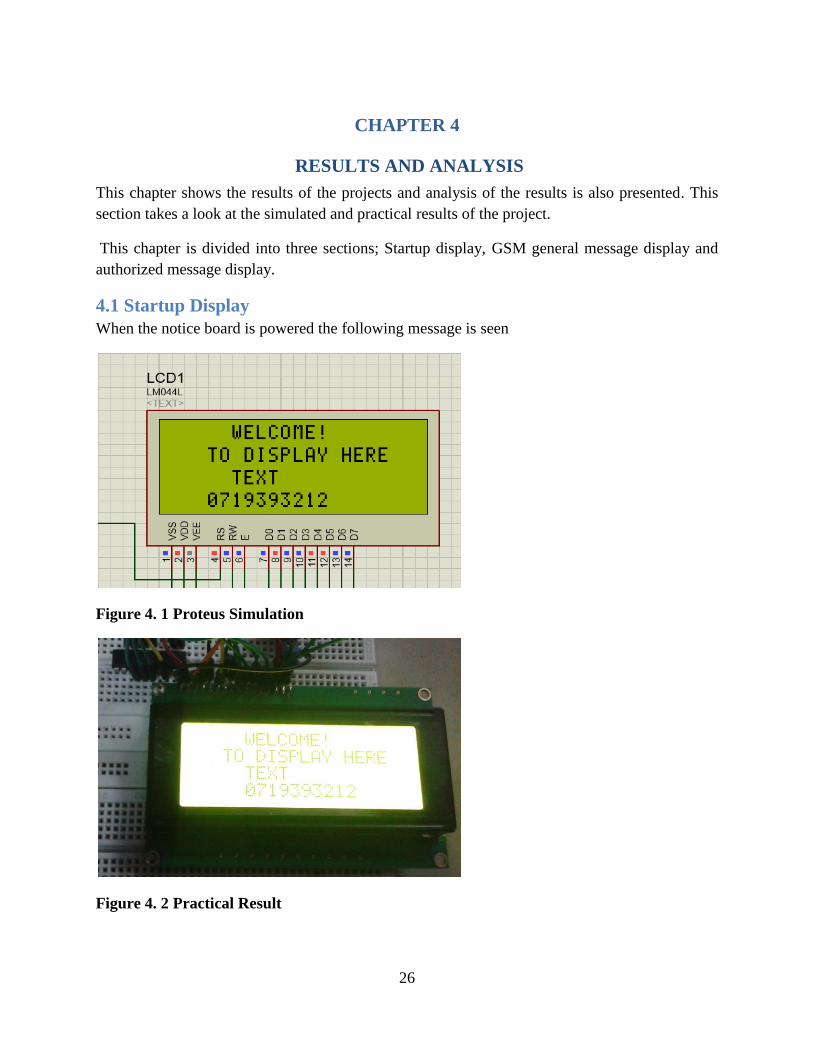
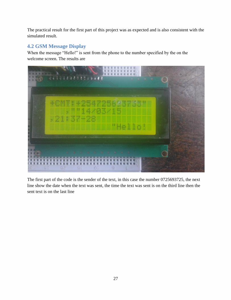
4.1 Startup Display
When the notice board is powered the following message is seen
Figure 4. 1 Proteus Simulation
Figure 4. 2 Practical Result
27
The practical result for the first part of this project was as expected and is also consistent with the
simulated result.
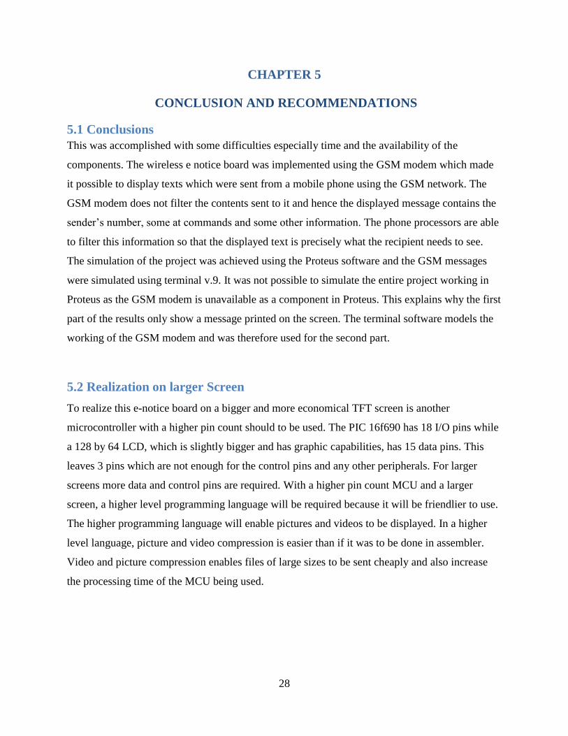
4.2 GSM Message Display
When the message “Hello!” is sent from the phone to the number specified by the on the
welcome screen. The results are
The first part of the code is the sender of the text, in this case the number 0725693725, the next
line show the date when the text was sent, the time the text was sent is on the third line then the
sent text is on the last line
28
CHAPTER 5
CONCLUSION AND RECOMMENDATIONS
5.1 Conclusions
This was accomplished with some difficulties especially time and the availability of the
components. The wireless e notice board was implemented using the GSM modem which made
it possible to display texts which were sent from a mobile phone using the GSM network. The
GSM modem does not filter the contents sent to it and hence the displayed message contains the
sender’s number, some at commands and some other information. The phone processors are able
to filter this information so that the displayed text is precisely what the recipient needs to see.
The simulation of the project was achieved using the Proteus software and the GSM messages
were simulated using terminal v.9. It was not possible to simulate the entire project working in
Proteus as the GSM modem is unavailable as a component in Proteus. This explains why the first
part of the results only show a message printed on the screen. The terminal software models the
working of the GSM modem and was therefore used for the second part.
5.2 Realization on larger Screen
To realize this e-notice board on a bigger and more economical TFT screen is another
microcontroller with a higher pin count should to be used. The PIC 16f690 has 18 I/O pins while
a 128 by 64 LCD, which is slightly bigger and has graphic capabilities, has 15 data pins. This
leaves 3 pins which are not enough for the control pins and any other peripherals. For larger
screens more data and control pins are required. With a higher pin count MCU and a larger
screen, a higher level programming language will be required because it will be friendlier to use.
The higher programming language will enable pictures and videos to be displayed. In a higher
level language, picture and video compression is easier than if it was to be done in assembler.
Video and picture compression enables files of large sizes to be sent cheaply and also increase
the processing time of the MCU being used.
29
5.3 Recommendations
With assembler language, the amount of material being sent to the screen from the GSM modem
is a lot and most of it is irrelevant to the target audience. When a higher level language is used
the content can be edited to be precise as possible. The display unit used in this project is a 20 by
4 LCD screen and this does not allow for graphic changes and picture to be displayed. For future
work of a similar project, a bigger screen should be used so display is not limited to text
messages only. 29 the GSM modem has other functionalities that can be used to make the notice
board more functional. For example the GSM modem has the capacity to read and write
messages, delete messages from the SIM card and it can also make and receive calls. Future
works should explore these functions.

30
31
BIBLIOGRAPHY
[1] M. Joshi, "EnTcians," Students of E&TC, 25 July 2013. [Online]. Available: electro-
mate.blogspot.com/2013/07/classification-of-microcontrollers.html. [Accessed 17 February
2015].
[2] T. Wilmhurst, Designing Embedded Systems with PIC Microcontrollers: Principles and
applications, Oxford: Elsevier, 2007.
[3] PIC16F631/677/685/687/689/690 Datasheet, USA: Microchip Technology, 2006.
[4] J. Morton, The PIC microcontroller: Your personal introductory course, Oxford: Jordan
Hill, 2005.
[5] M. Bates, PIC Microcontroller: An introductin to Microelectronics, Oxford: Elsevier, 2011.
[6] "Ali Express," [Online]. Available:
m.aliexpress.com/item/478350901.html?tracelog=storedetail2mobilesitedetail. [Accessed 18
February 2015].
[7] "Electronic Experimental Solutions," [Online]. Available:
www.gravitech.us/20chbllcd.html. [Accessed 17 February 2015].
[8] D. Ibrahim, PIC basic Projects: 30 projects using PICBASIC and PICBASIC PRO, Oxford:
Elservier, 2006.
[9] C. P. Sanchez.J, Microcrontroller Programming; The Microchip PIC, London: CRC Press,
2007.
[10] Michael.A.Covington, PIC Assembly language for the complete beginner, Athens:
Gernsback publications, 1999.
[11] "Ali Express," [Online]. Available:
m.aliexpress.com/item/1988030875.html?tracelog=storedetail2mobilesitedetail. [Accessed
18 February 2015].
[12] M. Verle, PIC Microcontrollers, Mikroelectronika.
[13] "PIC Tutorial Three- LCD modules," Winpicprog, june 2002. [Online]. Available:
www.winpicprog.co.uk/pic_tutorial.htm. [Accessed 12 March 2015].
32
[14] M. Bates, Interfacing PIC microcontrollers: Embedded design by interactive simulation,
Oxford: Elsevier, 2006.
[15] "SIM 900 modules," in SIM 900 datasheet.
[16] D. W. Smith, PIC in Practice: A Project based Approach, oxford: elsevier, 2006.
[17] "saving energy forcomputer monitors," [Online]. Available: www.hk-
phy.org/energy/commercial office_is03_e.html. [Accessed 17 February 2015].
33
APPENDIX
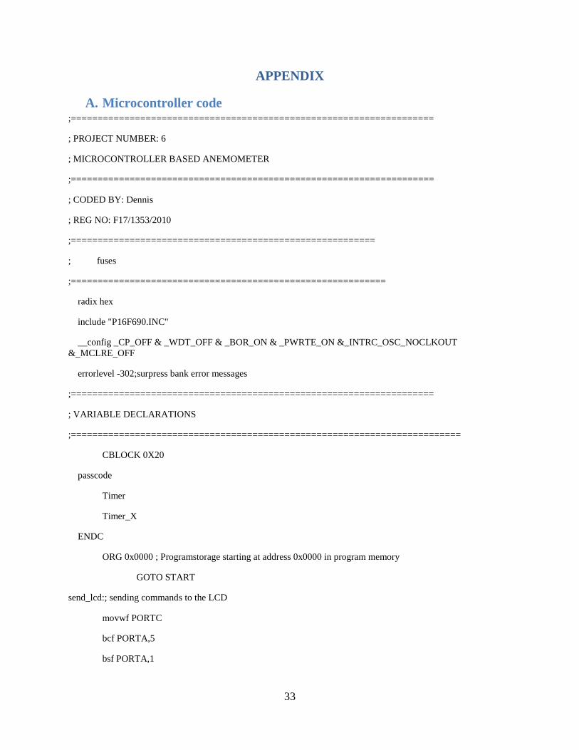
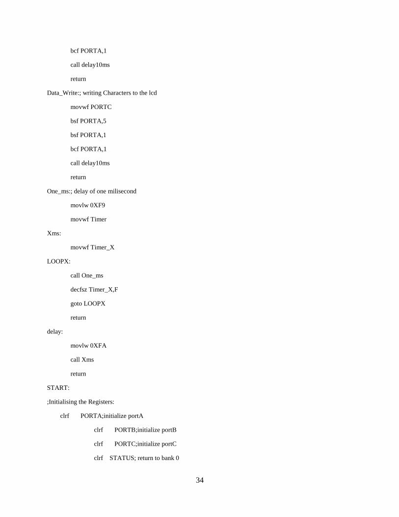
A. Microcontroller code ;====================================================================
; PROJECT NUMBER: 6
; MICROCONTROLLER BASED ANEMOMETER
;====================================================================
; CODED BY: Dennis
; REG NO: F17/1353/2010
;=========================================================
; fuses
;===========================================================
radix hex
include "P16F690.INC"
__config _CP_OFF & _WDT_OFF & _BOR_ON & _PWRTE_ON &_INTRC_OSC_NOCLKOUT
&_MCLRE_OFF
errorlevel -302;surpress bank error messages
;====================================================================
; VARIABLE DECLARATIONS
;=========================================================================
CBLOCK 0X20
passcode
Timer
Timer_X
ENDC
ORG 0x0000 ; Programstorage starting at address 0x0000 in program memory
GOTO START
send_lcd:; sending commands to the LCD
movwf PORTC
bcf PORTA,5
bsf PORTA,1
34
bcf PORTA,1
call delay10ms
return
Data_Write:; writing Characters to the lcd
movwf PORTC
bsf PORTA,5
bsf PORTA,1
bcf PORTA,1
call delay10ms
return
One_ms:; delay of one milisecond
movlw 0XF9
movwf Timer
Xms:
movwf Timer_X
LOOPX:
call One_ms
decfsz Timer_X,F
goto LOOPX
return
delay:
movlw 0XFA
call Xms
return
START:
;Initialising the Registers:
clrf PORTA;initialize portA
clrf PORTB;initialize portB
clrf PORTC;initialize portC
clrf STATUS; return to bank 0
35
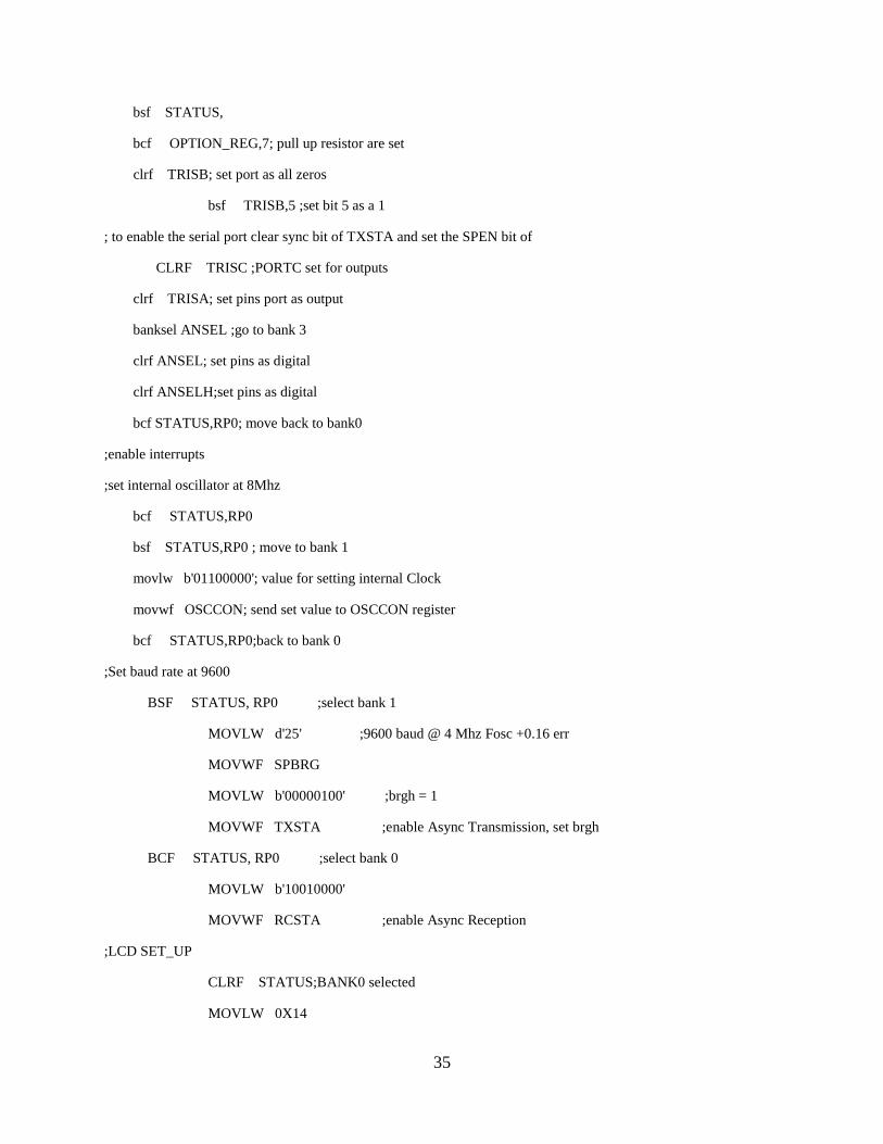
bsf STATUS,
bcf OPTION_REG,7; pull up resistor are set
clrf TRISB; set port as all zeros
bsf TRISB,5 ;set bit 5 as a 1
; to enable the serial port clear sync bit of TXSTA and set the SPEN bit of
CLRF TRISC ;PORTC set for outputs
clrf TRISA; set pins port as output
banksel ANSEL ;go to bank 3
clrf ANSEL; set pins as digital
clrf ANSELH;set pins as digital
bcf STATUS,RP0; move back to bank0
;enable interrupts
;set internal oscillator at 8Mhz
bcf STATUS,RP0
bsf STATUS,RP0 ; move to bank 1
movlw b'01100000'; value for setting internal Clock
movwf OSCCON; send set value to OSCCON register
bcf STATUS,RP0;back to bank 0
;Set baud rate at 9600
BSF STATUS, RP0 ;select bank 1
MOVLW d'25' ;9600 baud @ 4 Mhz Fosc +0.16 err
MOVWF SPBRG
MOVLW b'00000100' ;brgh = 1
MOVWF TXSTA ;enable Async Transmission, set brgh
BCF STATUS, RP0 ;select bank 0
MOVLW b'10010000'
MOVWF RCSTA ;enable Async Reception
;LCD SET_UP
CLRF STATUS;BANK0 selected
MOVLW 0X14

36
CALL Xms ;20ms time delay allows LCD to complete initialisation process.
MOVLW 0x01 ;Display clear command
CALL send_lcd
MOVLW 0x38
CALL send_lcd;LCD set for 8-bit, 2-Line,5x8 dot matrix display.
MOVLW 0x0c
CALL send_lcd ;Display on,Cursor off, no Blinking.
MOVLW 0x04
CALL send_lcd
MOVLW 0x01
CALL send_lcd;Display cleared,DDRAM address=0
MOVLW 0x85
CALL send_lcd ;DDRAM address set to 0
;WELCOME message sent to screen
movlw 0x57 ;'w'
call Data_Write
movlw 0x45 ;'E'
call Data_Write
movlw 0x4C ;'L'
call Data_Write
movlw 0x43 ;'C'
call Data_Write
movlw 0x4F ;'O'
call Data_Write
movlw 0x4D ;'M'
call Data_Write
movlw 0x45 ;'E'
call Data_Write
movlw 0x21 ;'!'
call Data_Write
37
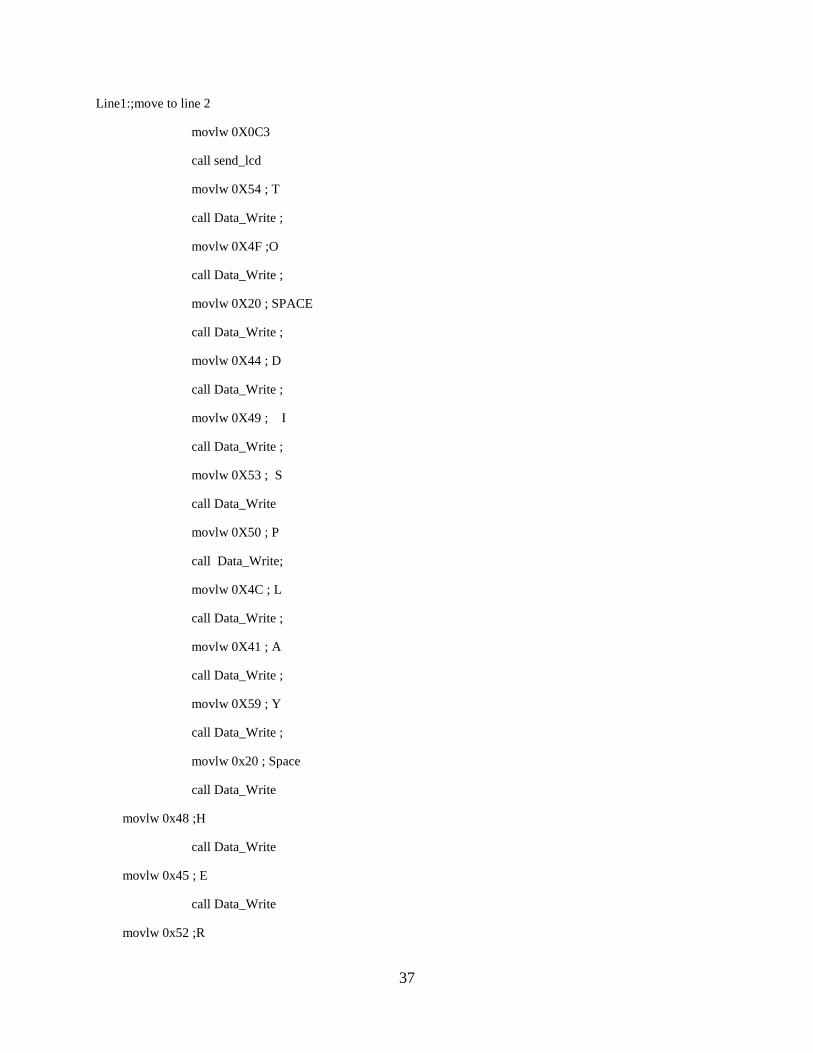
Line1:;move to line 2
movlw 0X0C3
call send_lcd
movlw 0X54 ; T
call Data_Write ;
movlw 0X4F ;O
call Data_Write ;
movlw 0X20 ; SPACE
call Data_Write ;
movlw 0X44 ; D
call Data_Write ;
movlw 0X49 ; I
call Data_Write ;
movlw 0X53 ; S
call Data_Write
movlw 0X50 ; P
call Data_Write;
movlw 0X4C ; L
call Data_Write ;
movlw 0X41 ; A
call Data_Write ;
movlw 0X59 ; Y
call Data_Write ;
movlw 0x20 ; Space
call Data_Write
movlw 0x48 ;H
call Data_Write
movlw 0x45 ; E
call Data_Write
movlw 0x52 ;R
38
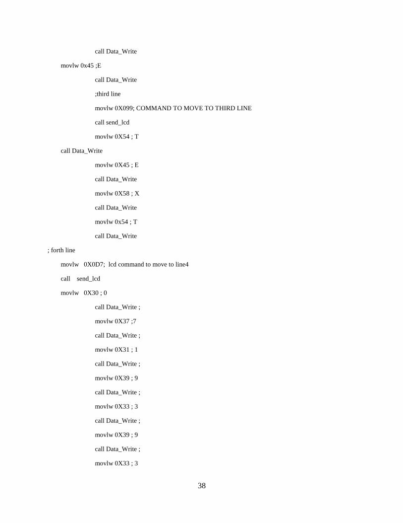
call Data_Write
movlw 0x45 ;E
call Data_Write
;third line
movlw 0X099; COMMAND TO MOVE TO THIRD LINE
call send_lcd
movlw 0X54 ; T
call Data_Write
movlw 0X45 ; E
call Data_Write
movlw 0X58 ; X
call Data_Write
movlw 0x54 ; T
call Data_Write
; forth line
movlw 0X0D7; lcd command to move to line4
call send_lcd
movlw 0X30 ; 0
call Data_Write ;
movlw 0X37 ;7
call Data_Write ;
movlw 0X31 ; 1
call Data_Write ;
movlw 0X39 ; 9
call Data_Write ;
movlw 0X33 ; 3
call Data_Write ;
movlw 0X39 ; 9
call Data_Write ;
movlw 0X33 ; 3
39
call Data_Write ;
movlw 0X32 ; 2
call Data_Write
movlw 0X31 ; 1
call Data_Write
movlw 0X32 ; 2
call Data_Write
movlw d'100';delay
call LOOPX
movlw d'100';wait
call LOOPX
movlw d'100'; wait
call LOOPX
movlw d'100'; wait
call LOOPX
LOOP:
call Rcv_RS232 ; function to receive from GSM
goto LOOP;recheck the above function
XMIT_RS232: ;transmitting
btfss PIR1, TXIF ;xmit buffer empty?
GOTO XMIT_RS232 ;no, wait
MOVWF TXREG ;now send
RETURN
Rcv_RS232:
BTFSS PIR1, RCIF ; check for received data
GOTO Rcv_RS232
40
MOVF RCREG, W; move received data to RCREG
CALL Data_Write
RETURN
END; end of entire program
41
B. PIC16f690 Internal Architecture
Appendix Figure 1. 1 Internal Architecture of PIC16F690 [3]
42
C. Circuit Diagram
43
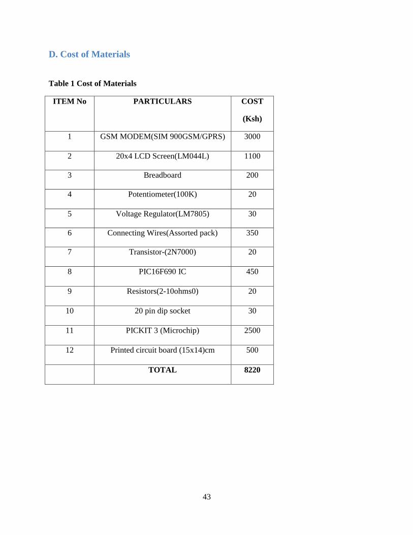
D. Cost of Materials
Table 1 Cost of Materials
ITEM No PARTICULARS COST
(Ksh)
1 GSM MODEM(SIM 900GSM/GPRS) 3000
2 20x4 LCD Screen(LM044L) 1100
3 Breadboard 200
4 Potentiometer(100K) 20
5 Voltage Regulator(LM7805) 30
6 Connecting Wires(Assorted pack) 350
7 Transistor-(2N7000) 20
8 PIC16F690 IC 450
9 Resistors(2-10ohms0) 20
10 20 pin dip socket 30
11 PICKIT 3 (Microchip) 2500
12 Printed circuit board (15x14)cm 500
TOTAL 8220