Embed Size (px)
Citation preview

University of Mumbai
A PROJECT ON
GSM Based Home Automation & Security
By
Kartik Bhat
V.Ananthasuri Amit More
Riddhi Shah
Under the guidance of
Prof. Dipali Joshi (Internal Guide) Prof. Hiral Shah (Internal Guide)
Department Of Instrumentation
Rajiv Gandhi Institute of Technology Versova, Andheri (West), Mumbai-400053
2008-2009

Department of Instrumentation, Rajiv Gandhi Institute of Technology,
Juhu – Versova Link Road ,Versova ,Andheri (w) Mumbai-53
2008-2009
This is to certify that
Kartik Bhat
V.Ananthasuri Amit More
Riddhi Shah
Have Satisfactory completed the project entitled
GSM Based Home Automation & Security
Towards the partial fulfillment of the
BACHELOR OF ENGINEERING IN
INSTRUMENTATION
As laid by University of Mumbai.
Internal Guide (Prof. Dipali Joshi) (Prof. Hiral Shah)
Examiner Head of department
Principal (Dr. N K Rana)
(Dr. U V Bhosle)

GSM BASED HOME AUTOMATION AND SECURITY
ACKNOWLEDGEMENT
The success of our project involves a lot of direct & indirect contribution from
a lot of people. It is difficult of thank all of them but we would like to thank the
most prominent ones.
First and foremost, we are extremely indebted to our internal guide Prof.
Dipali Joshi and co-guide Prof. Hiral Shah for showing faith in our project &
believing in our potential. Their guidance and suggestions were great source
of inspiration and motivation without which implementing this project would
have been impossible.
We would also like to thank Prof. N. K. Rana, our Head of the Department, in
instrumentation section with whose kind consent we could go ahead with this
project. He was very co-operative and provided all the support required to
accomplish such a task successfully.
We would also like to express our thanks to all the staff in general who co-
operated with us in this project. And last but not the least we would like to
thank our friends to help us at various times of our difficulties.
Project team members:
Kartik Bhat.
V. Ananthasuri.
Amit More.
Riddhi Shah.

GSM BASED HOME AUTOMATION AND SECURITY
ii
ABSTRACT
We live in the world of uncertainties. Security has become one of the
most important and primary concern in our day-to-day life. There is always an element of danger in every point. Sometimes it is possible to avoid these conditions. We can control the magnitude of the destruction caused if it is not. The two main security concerns addressed in this project are theft and fire. These are the foremost concerns be it homes, offices, banks etc. The existing system involves human interaction on a very large scale. These systems have greater chance of failure because humans are prone to make errors. Imagine a situation when fire breaks out or a Burglary takes place. These incidents involve loss of property or even lives. These conditions demands quick thinking and immediate action. Otherwise destruction on a large scale would take place.
One thing in is clear now that the human intervention has made the existing security system impaired. Our aim is to eliminate or minimize the role played by the humans in the system. It should be as low as possible. This is where the role of GSM based Home Automation & Security System comes into play. What if the fire department is informed about the possibility of outbreak of fire? What if the Owner of the home or the Police are informed about the presence of an intruder? It would be clear in the next few chapters how by using modern scientific techniques we can take step into the world of improved security. We present you in this project the future of the security system. It involves a Burglar Alarm system and Fire alarm. It also has additional features like Temperature Controller and Light Intensity Controller. The purpose of the Temperature Controller is to keep the temperature of a room within a certain range. This range can be adjusted by the user. Light Intensity Controller is used to keep the intensity of light within a certain range. Again the range is adjustable as per the user’s choice. These features would be explained in detail in the forthcoming chapters.

GSM BASED HOME AUTOMATION AND SECURITY
iii
List of Figures
Figure 2-2.1 Block diagram of project 6
Figure 3-3.1a Full circuit diagram 11
Figure 3-3.1b Relay interfacing with microcontroller 12
Figure 3-3.1c Motor interfacing 13
Figure 3-3.1d Max232 interfacing 14
Figure 3-3.3a Pin diagram of P89C51 21
Figure 3-3.3b Block diagram of P89C51 22
Figure 3-3.3c Microcontroller interface 23
Figure 3-3.4a Block diagram of ADC0809 29
Figure 3-3.4b Pin diagram of ADC0809 29
Figure 3-3.5 LCD interfacing 31
Figure 3-3.6a Pole and throw 33
Figure 3-3.6b Basic diagram showing working of relay 35
Figure 3-3.7 Pin diagram of Max232 39
Figure 3-3.8a Pin diagram of motor L293D 42
Figure 3-3.8b Circuit diagram of L293D 43
Figure 3-3.9 Circuit diagram of Power supply 46
Figure 3-3.10 Circuit diagram of Keypad 48
Figure 3-3.11 LDR 50
Figure 3-3.12 LM35 52
Figure 4-4.1a Pin outs of Nokia 3310 58
Figure 4-4.1b F-bus connected to 3310 58
Figure 4-4.1c An F-bus cable 58
Figure 5-5.1 Basic block diagram of GSM system 69
Figure 5-5.2 Communication between BTS and BSC 71

GSM BASED HOME AUTOMATION AND SECURITY
iv
List of Tables
Table 3-3.3 Convention used for 8X51 19
Table 7-7.1 Comparison of various technologies 82

GSM BASED HOME AUTOMATION AND SECURITY
v
Table of Contents
SR.NO Page No
Acknowledgement i Abstract ii
List of figures iii List of tables iv
Chapter 1 Project Overview
1.1 Introduction 02
1.2 Motivation 03
1.3 Scope 04
Chapter 2 SYSTEM DESIGN
2.1 Block Diagram 06
2.2 General Description 07
2.3 Hardware Requirements 08
2.4 Software Requirements 09
Chapter 3 CIRCUIT DIAGRAM AND DESCRIPTION
3.1 Circuit Diagram 11
3.2 Description & Working 15
3.3 PHILIPS 89C51
Introduction to microcontrollers 18
Features 20
Pin Diagram 21
Internal Block Diagram 21
Microcontroller Interface 22
3.4 ADC 0809
Block Diagram 24
Pin Diagram 24

GSM BASED HOME AUTOMATION AND SECURITY
vi
General Description 25
Features 25
3.5 LIQUID CRYSTAL DISPLAY (LCD)
General Description 28
LCD Interface 29
3.6 RELAYS
General Description 31
Operation 33
Applications of Relay 35
3.7 MAX232
General Description 36 Features 37 PIN Diagram 37
3.8 MOTOR DRIVER (L293D)
General Description 39 Features 39 Pin diagram 40 Working 41
3.9 POWER SUPPLY
Design 43 Circuit Diagram 44
3.10 KEYPAD
Circuit Diagram 46 Description 46
3.11 LDR
General Description 47
3.12 LM35
General Description 50 Features 50 3.13 SMOKE SENSOR
General Description 51
Chapter 4 F-BUS COMMUNICATION
4.1 Introduction to Nokia F-Bus 54

GSM BASED HOME AUTOMATION AND SECURITY
vii
4.2 F-Bus Protocol 56 4.3 How to Send a SMS 59 4.4 Receiving a SMS 61 4.5 Deleting a SMS 63
Chapter 5 GSM SYSTEM
5.1 Basic Architecture 65 5.2 GSM Security 69 5.3 Subscriber Identification Module (SIM) 70
Chapter 6 SOFTWARE AND FLOWCHARTS
6.1 Flow Charts 72 6.2 KEIL 75
Chapter 7 SYSTEM ANALYSIS
7.1 Comparison between Various Technologies 78
7.2 GSM Based Automation Features over Current Systems 79
Chapter 8 POSSIBLE ENHANCEMENTS 80
Chapter 9 RESULTS AND CONCLUSION 81
APPENDIX
Layouts Datasheets Bibliography

GSM BASED HOME AUTOMATION AND SECURITY
- 1 -
Chapter 1
Project Overview
Introduction
Motivation
Scope

GSM BASED HOME AUTOMATION AND SECURITY
- 2 -
1.1
Introduction
Now-a-days, life style has become very fast and busy and it is not possible to
continuously track the alarming events. Hence, the automation of capturing the events
and communicating them has become necessity. To achieve this we have developed
the system named GSM BASED HOME AUTOMATION & SECURITY. If a particular
sensor detects a failure of a system then the system generates an alarming event and
depending upon the severity it sends respective SMS to the configured mobile number
of a concerned person. Depending upon the type of the event the person can take
further action.
This system can be used in many applications. Here, we are presenting
general Security System for offices or company or home. For this, we have used
smoke detector, Light dependent resistor, Temperature sensor and keypad based
lock. The slave mobile is connected to the Micro controller via the F-BUS cable and
serial port. Remote controlling is done by the remote master mobile. The specific SMS
is sent from the master mobile to the slave mobile through a regular GSM network.
The Micro controller interprets the received message from the slave mobile and
initiates the required action. An acknowledgement signal is then generated by the
Micro controller which is sent back to the master mobile as a regular SMS.
The Micro controller will continuously check the status of the sensors. If any of
the sensor’s condition breaks, then the Microcontroller detects that and sends
respective SMS through Mobile to the concerned person, so that the person can take
further action.

GSM BASED HOME AUTOMATION AND SECURITY
- 3 -
1.2
Motivation
Many of the current security and monitoring systems available till now requires
manual intervention and not all of them real time and don’t support 24 hour
monitoring. Where the manual intervention is, there will be little pinch for errors. The
GSM based Automation system provides easy accessibility and complete automation
of the system. The mobile network is on the path of continual improvement. The
betterment of this system for the end user is the main aim of the project. As the mobile
has become an integral part of our lives, the choice of this project seems all the more
logical.
GSM BASED HOME AUTOMATION AND SECURITY
- 4 -
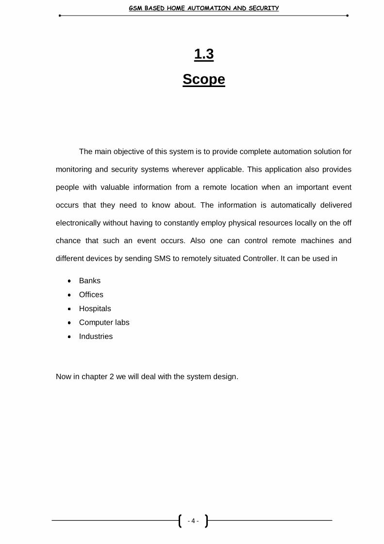
1.3
Scope
The main objective of this system is to provide complete automation solution for
monitoring and security systems wherever applicable. This application also provides
people with valuable information from a remote location when an important event
occurs that they need to know about. The information is automatically delivered
electronically without having to constantly employ physical resources locally on the off
chance that such an event occurs. Also one can control remote machines and
different devices by sending SMS to remotely situated Controller. It can be used in
Banks
Offices
Hospitals
Computer labs
Industries
Now in chapter 2 we will deal with the system design.

GSM BASED HOME AUTOMATION AND SECURITY
- 5 -
Chapter 2
System Design
Block diagram
Specifications
Hardware requirement
Software requirement

GSM BASED HOME AUTOMATION AND SECURITY
- 6 -
2.1
Block Diagram
Figure 2-2.1 Block diagram of project

GSM BASED HOME AUTOMATION AND SECURITY
- 7 -
2.2
General Description
The block diagram show above contains 4 blocks before the signal conditioning block
and these blocks are
Fire sensor: In this project we have used ionization type smoke detector which
will continuously check for fire in the place of its installation.
Temperature control: In this project we have used LM35 as temperature
sensor which will continuously check the temperature and give its output to
microcontroller through ADC. Two relays will switch the heater and the cooler
respectively according to temperature preset.
Anti theft device: In this project we have used keypad based locking system,
where in the user has to enter the pre-defined password to open the door. User
gets 3 attempts to enter correct password.
Light control: In this project we have used LDR (light dependent resistor) to
control the lighting of the room based on the intensity. Lights will switch ON-
OFF according to some predefined intensity level.
For GSM module we are using Nokia 3310 with an F-bus cable and it serves
the purpose of GSM interface with microcontroller.
For purpose of display we are using 16*2 LCD display which gives information
about various activities happening in the microcontroller and peripheral
devices.
Microcontroller used here is Philips P89C51.
Buzzer is used to bring to attention some undesirable event that is going to
take place.
GSM BASED HOME AUTOMATION AND SECURITY
- 8 -
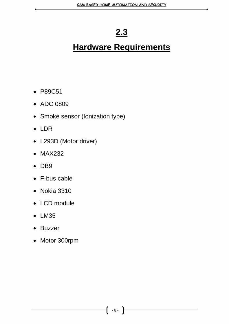
2.3
Hardware Requirements
P89C51
ADC 0809
Smoke sensor (Ionization type)
LDR
L293D (Motor driver)
MAX232
DB9
F-bus cable
Nokia 3310
LCD module
LM35
Buzzer
Motor 300rpm
GSM BASED HOME AUTOMATION AND SECURITY
- 9 -
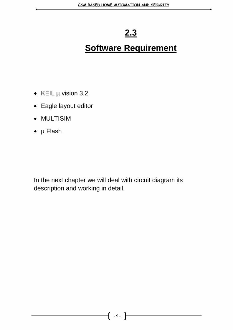
2.3
Software Requirement
KEIL µ vision 3.2
Eagle layout editor
MULTISIM
µ Flash
In the next chapter we will deal with circuit diagram its
description and working in detail.

GSM BASED HOME AUTOMATION AND SECURITY
- 10 -
Chapter 3
Circuit Diagram and Description
Circuit diagram
Description & working
Philips P89C51
ADC 0809
Liquid crystal display (LCD)
Relays
MAX 232
Power supply
Keypad
LDR
LM 35
Smoke sensor

GSM BASED HOME AUTOMATION AND SECURITY
- 11 -
3.1
Circuit diagram
Figure 3-3.1a Full Circuit diagram

GSM BASED HOME AUTOMATION AND SECURITY
- 12 -
Relays Interfacing with Microcontroller
Figure 3-3.1b Relay interfacing

GSM BASED HOME AUTOMATION AND SECURITY
- 13 -
Motor Interfacing
Figure 3-3.1c Motor interfacing

GSM BASED HOME AUTOMATION AND SECURITY
- 14 -
Max 232 Interfacing
Figure 3-3.1d Max 232 interfacing
X1A is connected to port 3.1 of microcontroller
X1B is connected to port 3.0 of microcontroller

GSM BASED HOME AUTOMATION AND SECURITY
Actual photo of the circuit with all devices connected.

GSM BASED HOME AUTOMATION AND SECURITY
- 15 -
3.2
Description and working
Circuit Description & Working
The above circuit shows the interfacing of the microcontroller with different
components. The components which are interfaced are LCD, ADC, Keypad, Relays,
Smoke sensor, LM35.
LCD: The LCD is connected to the Port 1 of the microcontroller. The pins P1.5 to P1.8
are the data lines. P1.2 to P1.4 is control lines. P1.2 is connected to WR (write) pin,
P1.3 is connected to RD (read) pin and P1.4 to enable pin.
ADC: ADC is used to convert the input analog signal to digital signal. It is connected to
the Port 0 of the microcontroller. The ADC gets the analog signal from the
temperature sensor and LDR. Timer is used to provide clock pulses to ADC used in
the conversion of analog signals to digital signals.
Keypad: Keypad is a component useful in the Anti Theft system. It is connected to the
Port 2 of the microcontroller. The user uses keypad to enter the password. The user
must enter the correct password in order to enter the house. The keypad used here is
3*3 keypad.
Smoke detector: Smoke detector used is an ionization type detector. It is connected to
ort 2.3 of microcontroller.
LM35: It is temperature sensor used to constantly monitor temperature inside the
room. It is connected to channel 2 of ADC 0809.
LDR: it is used for automatic light controlling and continuously senses for change in
light intensity. It is connected to channel 1 of ADC.
GSM BASED HOME AUTOMATION AND SECURITY
- 16 -
Working:
The system we have designed works as a real time system which keeping on
scanning the current condition with the one which is preset in the microcontroller to
check if there is any undesirable condition. If there is any undesirable condition it
takes corrective action accordingly for e.g. if the temperature passes the set range of
20-40 and it goes down to say 18 in this case we have predefined to turn ON the
cooler till temperature becomes greater than or equal to 20 i.e. bringing it back to pre
defined range.
Similarly we have done it for automatic lighting where if the intensity of light
falls below dome predefined range the microcontroller switches on the relay and
hence the light thus compensating for fall in intensity of light.
We have used a smoke sensor to continuously monitor if the house is safe from
any fire hazardous. The sensor used is an ionic type sensor whose working is
explained in detail in section 3.13. The sensor checks for hazardous condition and
immediately brings it to notice of the owner if there is any breakthrough.
Similar sort of arrangement is made for security by using keypad based locking
of the door which acts as burglar alarm system. Only genuine user can enter the room
that has the correct password. The user gets 3 attempts to enter correct password if
he fails to enter it correctly the buzzer starts to ring and immediately this is brought to
notice of the owner by sending him a warning message.
This is how the entire system works.
We will explain you function and working of each part in following subsections.

GSM BASED HOME AUTOMATION AND SECURITY
- 17 -
3.3
PHILIPS Micro-Controller
Introduction to Microcontrollers
Features of 89C51
Pin Diagram of 89C51
Architecture of 89C51

GSM BASED HOME AUTOMATION AND SECURITY
- 18 -
Introduction to Microcontrollers
Definition
An embedded microcontroller is a chip which has a computer processor with all
its support functions (clock & reset), memory (both program and data), and I/O
(including bus interface) built into the device. These built in functions minimize the
need for external circuits and devices to be designed in the final application.
Types of Microcontroller
Creating applications for microcontrollers is completely different than any other
development job in computing and electronics. In most other applications one
probably have a number of subsystem and interfaces already available for his/her use.
This is not the case with a microcontroller where one is responsible for –
Power distribution
System clocking
Interface design and wiring
System programming
Application programming
Device programming
Before selecting a particular device for an application, it’ s important to understand
what the different options and features are and what they can mean with regard to
developing application.
Embedded Microcontroller
When all the hardware required to run the application is provided on the
chip, it is refer to as an Embedded Microcontroller. All that is typically required to
operate the device is power, reset, and a clock. Digital I/O pins are provided to allow
interfacing with external devices.

GSM BASED HOME AUTOMATION AND SECURITY
- 19 -
External Memory Microcontroller
Sometimes, the program memory is insufficient for an application or, during
debug; a separate ROM (or even RAM) would make the work easier. Some
microcontrollers including the 8051 allow the connection of external memory.
An external memory microcontroller seems to primarily differ from a
microprocessor in the areas of built-in-peripheral features. These features could
include memory device selection (avoiding the need for external address decoders or
DRAM address multiplexers), timers, interrupt controllers, DMA, and I/O devices like
serial ports.
Microcontroller Memory Types
There are number of different types of control store (Program Memory) that are
available in different versions and different manufacturers’ 8051s. The following is
the list of conventions used for 8X51-
Table 3-3.3 conventions used for 8X51
“X” value Control Store Type
0 None
3 Mask ROM
7 EPROM
9 EEPROM/FLASH

GSM BASED HOME AUTOMATION AND SECURITY
- 20 -
Features of 89C51
80C51 Central Processing Unit
On-chip FLASH Program Memory
Speed up to 33 MHz
Fully static operation
RAM expandable externally up to 64 Kbytes
4 interrupt priority levels
6 interrupt sources
Four 8-bit I/O ports
Full-duplex enhanced UART
Framing error detection
Automatic address recognition
Three 16-bit timers/counters T0, T1 (standard 80C51) and
Additional T2 (capture and compare)
Power control modes
Clock can be stopped and resumed
Idle mode
Power down mode
Programmable clock out
Second DPTR register
Asynchronous port reset
Low EMI (inhibit ALE)
Wake up from power down by an external interrupt

GSM BASED HOME AUTOMATION AND SECURITY
- 21 -
Pin Diagram of 89C51
Figure 3-3.3a Pin Diagram of P89C51
Internal Block Diagram
Figure 3-3.3b Block Diagram of P89C51

GSM BASED HOME AUTOMATION AND SECURITY
- 22 -
Microcontroller Interface
Figure 3-3.3c Micro Controller Interface

GSM BASED HOME AUTOMATION AND SECURITY
- 23 -
3.4
ADC 0808/0809
Block Diagram
Pin Diagram
General Description
Features

GSM BASED HOME AUTOMATION AND SECURITY
- 24 -
Block Diagram
Figure 3-3.4a block diagram of ADC
Pin diagram
Figure 3-3.4b Pin Diagram of ADC 0809

GSM BASED HOME AUTOMATION AND SECURITY
- 25 -
General description
The ADC0808, ADC0809 data acquisition component is a monolithic CMOS device
with an 8-bit analog-to-digital converter, 8-channel multiplexer and microprocessor
compatible control logic. The 8-bit A/D converter uses successive approximation as
the conversion technique. The converter features a high impedance chopper
stabilized comparator, a 256R voltage divider with analog switch tree and a
successive approximation register. The 8-channel multiplexer can directly access any
of 8-single-ended analog signals. The device eliminates the need for external zero
and full-scale adjustments. Easy interfacing to microprocessors is provided by the
latched and decoded multiplexer address inputs and latched TTL TRI-STATE®
outputs.
The ADC0808, ADC0809 offers high speed, high accuracy, minimal
temperature dependence, excellent long-term accuracy and repeatability, and
consumes minimal power. These features make this device ideally suited to
applications from process and machine control to consumer and automotive
applications.
Features
Easy interface to all microprocessors
Operates ratiometrically or with 5 VDC or analog span
Adjusted voltage reference
No zero or full-scale adjust required
8-channel multiplexer with address logic
0V to 5V input range with single 5V power supply
Outputs meet TTL voltage level specifications

GSM BASED HOME AUTOMATION AND SECURITY
- 26 -
Standard hermetic or molded 28-pin DIP package
28-pin molded chip carrier package
ADC0808 equivalent to MM74C949
ADC0809 equivalent to MM74C949-1
Key Specifications
Resolution 8 Bits
Total Unadjusted Error ±1⁄2 LSB and ±1 LSB
Single Supply 5 VDC
Low Power 15 mW
Conversion Time 100 μs

GSM BASED HOME AUTOMATION AND SECURITY
- 27 -
3.5
LIQUID CRYSTAL DISPLAY (LCD)
General description
Features
Interfacing

GSM BASED HOME AUTOMATION AND SECURITY
- 28 -
General description
LCD’s are passive display having low power consumption and contrast ratio. The
characteristic of LCD’s are given below:
LCD’s operate on the principle of light scattering. They can be operated either in a
reflective or transmissive configuration. There operation dependent on ambient or
back lightering as they do not generate their own light. It operates on low voltage
around 1v-5v and the power required by LCD to the scatter or absorbs light is very
low in the order of the few micro-watts/cm.
A transmissive LCD has better visual characteristic than a reflective LCD.
The operation of LCD is base on the use of certain organic material, which retains
a regular crystal like structure even when they have been melted.
Nematic and cholestric are to important liquid crystal material used in display out of
these two NLC has a particular crystal structure. The liquid is normally transparent,
but if subjected to a strong electric field, an ion moves through it and disturbs the
well-ordered crystal structure. The liquid is normally transparent, but if subjected to
a strong electric field, ions move through it and disturb the well ordered crystal
structure causing the liquid to polarize and hence turn opaque.
Features
RS232 compatible serial interface (2400 & 9600 baud selectable)
Externally selectable serial polarities (Inverted & Non-Inverted)
Serially controllable contrast and backlight levels
8 user programmable custom characters
16 Byte serial receive buffer
5 x 8 dots with cursor
Built-in controller (KS 0066 or Equivalent)
+ 5V power supply (Also available for + 3V)
1/16 duty cycle

GSM BASED HOME AUTOMATION AND SECURITY
- 29 -
Interfacing
Figure 3-3.5 LCD interfacing with Microcontroller in 4 bit mode

GSM BASED HOME AUTOMATION AND SECURITY
- 30 -
3.6
RELAYS
General description
Operation
Application

GSM BASED HOME AUTOMATION AND SECURITY
- 31 -
General description
A relay is an electrical switch that opens and closes under the control of
another electrical circuit. In the original form, the switch is operated by an
electromagnet to open or close one or many sets of contacts. It was invented by
Joseph Henry in 1835. Because a relay is able to control an output circuit of higher
power than the input circuit, it can be considered to be, in a broad sense, a form of an
electrical amplifier.
Pole and Throw
Figure 3-3.6a Pole and Throw
SPST - Single Pole Single Throw. These have two terminals which can be
connected or disconnected. Including two for the coil, such a relay has four
terminals in total. It is ambiguous whether the pole is normally open or normally
closed. The terminology "SPNO" and "SPNC" is sometimes used to resolve the
ambiguity.
SPDT - Single Pole Double Throw. A common terminal connects to either of two
others. Including two for the coil, such a relay has five terminals in total.
DPST - Double Pole Single Throw. These have two pairs of terminals. Equivalent
to two SPST switches or relays actuated by a single coil. Including two for the coil,
such a relay has six terminals in total. The poles may be Form A or Form B (or one
of each).

GSM BASED HOME AUTOMATION AND SECURITY
- 32 -
DPDT - Double Pole Double Throw. These have two rows of change-over
terminals. Equivalent to two SPDT switches or relays actuated by a single coil.
Such a relay has eight terminals, including the coil.
Since relays are switches, the terminology applied to switches is also applied to relays
Normally-open (NO) contacts connect the circuit when the relay is activated; the
circuit is disconnected when the relay is inactive. It is also called a Form A contact
or "make" contact.
Normally-closed (NC) contacts disconnect the circuit when the relay is activated; the circuit is connected when the relay is inactive. It is also called a Form B contact or "break" contact.

GSM BASED HOME AUTOMATION AND SECURITY
- 33 -
Operation of relay
Circuit 1 is a simple electromagnet which requires only a small current. When the
switch is closed, current flows and the iron rocker arm is attracted to the
electromagnet. The arm rotates about the central pivot and pushes the contacts
together. Circuit 2 is now switched on.
Figure 3-3.6b Basic diagram showing working of relay
Circuit 2 may have a large current flowing through it, to operate a powerful motor or
very bright light. When the switch is opened the electromagnet releases the rocker
arm and the spring moves the contacts apart. Circuit 2 is now switched off. The
advantage of using a relay is that a small current (circuit 1) can be used to switch on
and off a circuit with a large current (circuit2).
This is useful for two reasons:
(i) Circuit 1 may contain a component such as an LDR, which only uses small
currents.
(ii) Only the high current circuit needs to be made from thick wire.

GSM BASED HOME AUTOMATION AND SECURITY
- 34 -
A relay is used to operate the starter motor in cars and the heating circuit in diesel
engines.
Applications
To control a high-voltage circuit with a low-voltage signal, as in
some types of modems or audio amplifiers
To control a high-current circuit with a low-current signal, as in the
starter solenoid of an automobile,
To detect and isolate faults on transmission and distribution lines by
opening and closing circuit breakers (protection relays)

GSM BASED HOME AUTOMATION AND SECURITY
- 35 -
3.7
MAX 232
General description
Features
Pin diagram
GSM BASED HOME AUTOMATION AND SECURITY
- 36 -
General Description
When communicating with various micro processors one needs to convert the
RS232 levels down to lower levels, typically 3.3 or 5.0 Volts.
Serial RS-232 (V.24) communication works with voltages -15V to +15V for high
and low. On the other hand, TTL logic operates between 0V and +5V. Modern low
power consumption logic operates in the range of 0V and +3.3V or even lower
Thus the RS-232 signal levels are far too high TTL electronics, and the negative
RS-232 voltage for high can’t be handled at all by computer logic. To receive serial
data from an RS-232 interface the voltage has to be reduced. Also the low and
high voltage level has to be inverted.
The MAX232 from Maxim was the first IC which in one package contains the
necessary drivers and receivers to adapt the RS-232 signal voltage levels to TTL
logic. It became popular, because it just needs one voltage (+5V or +3.3V) and
generates the necessary RS-232 voltage levels.

GSM BASED HOME AUTOMATION AND SECURITY
- 37 -
Features of MAX232
Meets or Exceeds TIA/EIA-232-F and ITU
Recommendation V.28
Operates From a Single 5-V Power Supply
With 1.0-_F Charge-Pump Capacitors
Operates Up To 120 Kbit/s
Two Drivers and Two Receivers
±30-V Input Levels
Low Supply Current . . . 8 mA Typical
Applications
− TIA/EIA-232-F, Battery-Powered Systems,
Terminals, Modems, and Computers
Pin diagram of MAX 232:
Figure 3-3.7 Pin diagram of max 232

GSM BASED HOME AUTOMATION AND SECURITY
- 38 -
3.8
MOTOR DRIVER L293D
General description
Features
Pin diagram

GSM BASED HOME AUTOMATION AND SECURITY
- 39 -
General description:
The L293 and L293D are quadruple high-current half-H drivers. The L293 is designed
to provide bidirectional drive currents of up to 1 A at voltages from 4.5 V to 36 V. The
L293D is designed to provide bidirectional drive currents of up to 600-mA at voltages
from 4.5 V to 36 V. Both devices are designed to drive inductive loads such as relays,
solenoids, dc and bipolar stepping motors, as well as other high-current/high-voltage
loads in positive-supply applications.
All inputs are TTL compatible. Each output is a complete totem-pole drive circuit, with
a Darlington transistor sink and a pseudo-Darlington source. Drivers are enabled in
pairs, with drivers 1 and 2 enabled by 1,2EN and drivers 3 and 4 enabled by
3,4EN.When an enable input is high, the associated drivers are enabled and their
outputs are active and in phase with their inputs. When the enable input is low, those
drivers are disabled and their outputs are off and in the high-impedance state. With
the proper data inputs, each pair of drivers forms a full-H (or bridge) reversible drive
suitable for solenoid or motor applications.
On the L293, external high-speed output clamp diodes should be used for inductive
transient suppression.
A VCC1 terminal, separate from VCC2, is provided for the logic inputs to minimize device
power dissipation.

GSM BASED HOME AUTOMATION AND SECURITY
- 40 -
Features
Operation from 0°C to 70°C
600mA Output Current Capability
Per Channel
1.2A Peak Output Current (Non Repetitive)
Per Channel
Enable Facility
Over Temperature Protection
Logical "0" Input Voltage Up To 1.5 V
(High Noise Immunity)
Internal Clamp Diodes
Pin diagram
Figure 3-3.8 a Pin diagram of motor driver L293D
GSM BASED HOME AUTOMATION AND SECURITY
- 41 -
Working:
Figure 3-3.8b Circuit diagram of motor driver L293D
This schematic shows the use of L293D to drive a pair of DC motors/Geared
Motors. The motor supply voltage can go up to 24Volts safely. But remember that
the IC supports a maximum of only 600mA current/channel which is more than
enough to drive small DC geared motors.
Remember to add 0.22uF capacitors across both the motors to reduce the effect of
noise on the circuitry.
It is also recommended to add 100uF capacitor between the motor supply pin and
the Gnd.
Connections M1-A and M2-B correspond to Motor 1 while connections M2-A and
M2-B correspond to Motor 2.
M1a=logic 0 and M1b= logic 1, motor runs in one direction.
M1a=logic1 and M1b= logic 0, motors run in reverse direction.
M1a = M1b= 0 motor stops running.
GSM BASED HOME AUTOMATION AND SECURITY
- 42 -
3.9
Power Supply
Design
Circuit diagram

GSM BASED HOME AUTOMATION AND SECURITY
- 43 -
Design
The system demanded an output of 5V dc and 12V dc.
We have used a bridge rectifier circuit along with 15V step down transformer.
Two IC’s namely IC 7805 and IC 7812 are used whose output is 5V and 12V dc
respectively.
5V supply is needed to microcontroller, LCD, MAX 232, Motor driver.
12V supply is needed for relays and Motor driver.

GSM BASED HOME AUTOMATION AND SECURITY
- 44 -
Circuit diagram:
Figure 3-3.9 circuit diagram of Power Supply

GSM BASED HOME AUTOMATION AND SECURITY
- 45 -
3.10
Keypad
Description
Circuit diagram

GSM BASED HOME AUTOMATION AND SECURITY
- 46 -
Description
Keypad is basically a matrix of many rows and columns. The number of pin
outs of keypad equals the sum of number of rows and columns in the keypad, with
each pin attached to a particular, unique, entire row or entire column via a naked tiny
conducting wire. All the wires are properly insulated from each other, however, at the
places where a wire for a column crosses a wire representing a row, there is a short
air-spacing between the two, instead of some insulated material, so that the two wires
do not touch each other at their own, but may be made to do so on key press. That is
where we press the keys on the keypad. As we press a particular key on the keypad,
the spacing between two wires reduces until the two wires, of one particular row and
one particular column, touch each other. Different scanning techniques may be
developed to determine which key is pressed (generally termed as keypad scanning).
Circuit diagram
Figure 3-3.10 Circuit diagram of Keypad

GSM BASED HOME AUTOMATION AND SECURITY
- 47 -
3.11
Light Dependent Resistor (LDR)
General description
LIGHT DEPENDENT RESISTOR
A photo resistor or light dependent resistor or cadmium sulfide (CdS) cell is a resistor
whose resistance decreases with increasing incident light intensity. It can also be
referenced as a photoconductor.
A photo resistor is made of a high resistance
semiconductor. If light falling on the device is of high
enough frequency, photons absorbed by the
semiconductor give bound electrons enough energy to
jump into the conduction band. The resulting free
electron (and its hole partner) conduct electricity,
thereby lowering resistance.
An intrinsic semiconductor has its own charge carriers
and is not an efficient semiconductor, e.g. silicon. In
intrinsic devices the only available electrons are in the
valence band, and hence the photon must have enough
energy to excite the electron across the entire band gap.
Extrinsic devices have impurities, also called dopants,
added whose ground state energy is closer to the
conduction band; since the electrons do not have as far
to jump, lower energy photons (i.e., longer wavelengths
and lower frequencies) are sufficient to trigger the
device. If a sample of silicon has some of its atoms
replaced by phosphorus atoms (impurities), there will be
extra electrons available for conduction.
Figure 3-3.11 LDR

GSM BASED HOME AUTOMATION AND SECURITY
- 48 -
A photo resistor is a sensor whose resistance varies with light intensity. Most
decrease in resistance as the light intensity increases. In a typical microcontroller
application, this resistance must be converted to a voltage so that an A2D converter
can measure it. The easiest way to do this is with a voltage divider circuit.
GSM BASED HOME AUTOMATION AND SECURITY
- 49 -
3.12
LM 35 (Temperature sensor)
Description
Features

GSM BASED HOME AUTOMATION AND SECURITY
- 50 -
Description
Figure 3-3.12 LM35
The LM35 series are precision integrated-circuit temperature sensors, whose output
voltage is linearly proportional to the temperature in degree Celsius. The LM35 thus
has an advantage over linear temperature sensors calibrated in ° Kelvin, as the user is
not required to subtract a large constant voltage from its output to obtain convenient
Centigrade scaling. The LM35 does not require any external calibration or trimming to
provide typical accuracies of ±¼°C at room temperature and ±¾°C over a full -55 to
+150°C temperature range. Low cost is assured by trimming and calibration at the
wafer level. The LM35's low output impedance, linear output, and precise inherent
calibration make interfacing to readout or control circuitry especially easy. It can be
used with single power supplies, or with plus and minus supplies. As it draws only
60 µA from its supply, it has very low self-heating, less than 0.1°C in still air. The
LM35 is rated to operate over a -55° to +150°C temperature range, while the LM35C
is rated for a -40° to +110°C range (-10° with improved accuracy).
Features:
Calibrated directly in ° Celsius (Centigrade)
Linear + 10.0 mV/°C scale factor
0.5°C accuracy (at +25°C)
Rated for full −55° to +150°C range
Operates from 4 to 30 volts
Less than 60 μA current drain
Low self-heating, 0.08°C in still air
Nonlinearity only ±1⁄4°C typical
Low impedance output, 0.1 W for 1 mA load
GSM BASED HOME AUTOMATION AND SECURITY
- 51 -
3.13
Smoke Detector
Description & Working:
A smoke detector is a device that detects smoke and issues a signal to a fire alarm
system, or issues a local audible and/or visual alarm from the detector itself.
A household smoke detector will typically be mounted in a disk-shaped plastic
enclosure about 150 millimeters (6 in) in diameter and 25 millimeters (1 in) thick, but
the shape can vary by manufacturer. Most smoke detectors work either by optical
detection (photoelectric) or by physical process (ionization), but some of them use
both detection methods to increase sensitivity to smoke.
Working of Ionization Smoke Detector:
Ionization smoke detectors use an ionization chamber and a source of ionizing
radiation to detect smoke. This type of smoke detector is more common
because it is inexpensive and better at detecting the smaller amounts of smoke
produced by flaming fires.
Inside ionization detector is a small amount (perhaps 1/5000th of a gram)
of americium-241. The radioactive element americium has a half-life of 432
years, and is a good source of alpha particles.
GSM BASED HOME AUTOMATION AND SECURITY
- 52 -
An ionization chamber is very simple. It consists of two plates with a voltage
across them, along with a radioactive source of ionizing radiation, like this:
The alpha particles generated by the americium have the following property:
They ionize the oxygen and nitrogen atoms of the air in the chamber. To
"ionize" means to "knock an electron off of." When you knock an electron off of
an atom, you end up with a free electron (with a negative charge) and an atom
missing one electron (with a positive charge). The negative electron is attracted
to the plate with a positive voltage, and the positive atom is attracted to the
plate with a negative voltage (opposites attract, just like with magnets). The
electronics in the smoke detector sense the small amount of electrical
current that these electrons and ions moving toward the plates represent.
When smoke enters the ionization chamber, it disrupts this current the smoke
particles attach to the ions and neutralize them. The smoke detector senses the
drop in current between the plates and sets off the horn.

GSM BASED HOME AUTOMATION AND SECURITY
- 53 -
Chapter 4
F-Bus Communication
Introduction to Nokia F-Bus
F-Bus Protocol
Sending a SMS
Receiving a SMS
Deleting a SMS

GSM BASED HOME AUTOMATION AND SECURITY
- 54 -
4.1
An Introduction to Nokia F-Bus
How to connect microcontrollers to Nokia 3310 & 3315
Most Nokia phones have F-Bus and M-Bus connections that can be used to
connect a phone to a PC or in our case a microcontroller. The connection can be used
for controlling just about all functions of the phone, as well as uploading new firmware
etc. This bus will allow us to send and receive SMS messages.
Figure 4-4.1a pin outs of NOKIA 3310 Figure 4-4.1b F-bus connected to 3310
The very popular Nokia 3310/3315 has the F/M Bus connection under the
battery holder. This is a bit of a pain to get to and requires a special cable to make the
connection.
Figure 4-4.1c An F-bus cable

GSM BASED HOME AUTOMATION AND SECURITY
- 55 -
The left picture above shows the 4 gold pads used for the F and M Bus. The
right picture shows the F-Bus cable connected to Nokia 3310.
Nokia download cables are available from most mobile phone shops and some
electronics stores. The cable contains electronics to level convert 3V signals to RS232
type signals. There are also M and F bus switching in most cables.
The differences of M-Bus and F-Bus
M-Bus is a one pin bi-directional bus for both transmitting and receiving data
from the phone. It is slow (9600bps) and only half-duplex. Only two pins on the phone
are used. A ground pin and one data pin. M-Bus runs at 9600bps, 8 data bits, odd
parity, and one stop bit. The data terminal ready (DTR) pin must be cleared with the
request to send (RTS).
F-Bus is the later high-speed full-duplex bus. It uses one pin for transmitting
data and one pin for receiving data plus the ground pin. Very much like a standard
serial port. It is fast 115,200bps, 8 data bits, no parity, and one stop bit. For F-Bus the
data terminal ready (DTR) pin must be set and the request to send (RTS) pin cleared.

GSM BASED HOME AUTOMATION AND SECURITY
- 56 -
4.2
F-Bus Protocol
The F-Bus is bi-directional serial type bus running at 115,200bps, 8 data bits.
The serial cable contains electronics for level conversion and therefore requires
power. The first thing to do is supply power to the cable electronics and this is done by
setting the DTR (Data Terminal Ready) pin and clearing the RTS (Request to Send)
pin.
Connect the DTR pin to a +3 to 12 Volt supply and RTS to a -3 to -12Volt
supply. The easy way to achieve this is by using a Max232 or similar transceiver for
the RS232 TX and RX pins and then connecting the DTR pin on the serial cable to the
V+ pin on the Max232. Do the same for the RTS; however connect it to the V- pin on
the Max232. The V+ and V- pins are derived from internal charge pumps that double
the input voltage. I.e. for a 5V Max232, the V+ will +10V and the V- will be -10V.
The next step is to synchronize the UART in the phone with microcontroller.
This is done by sending a string of 0x55 or 'U' 128 times. The bus is now ready to be
used for sending frames.
The Nokia protocol has a series of commands that allow the user to make calls,
send and get SMS messages and lots more.
Sample frame sent to Nokia 3310 (showed as a Hex dump)
Byte 00 01 02 03 04 05 06 07 08 09 10 11 12 13 14 15
Data 1E 00 0C D1 00 07 00 01 00 03 00 01 60 00 72 D5
This sample frame is used to get the hardware and software version from a
Nokia phone.
Byte 0: All frames sent by cable will start with the character 0x1E first. This is the F-
Bus Frame ID. Cable is 0x1E and Infrared is 0x1C.

GSM BASED HOME AUTOMATION AND SECURITY
- 57 -
Byte 1: This is the destination address. When sending data, it's the phone's device ID
byte. In our case it's always 00 for the phone.
Byte 2: This is the source address. When sending data, it's the PC's device ID byte.
In our case it's always 0x0C (Terminal).
Byte 3: This is the message type or 'command'. 0xD1 is Get HW & SW version.
Byte 4 & 5: Byte 4 & 5 is the message length. In our case it is 7 bytes long. Byte 4 is
the MSB and byte 5 is the LSB.
Byte 6: The data segment starts here and goes for 7 bytes in our case. As The Nokia
is a 16 bit phone and therefore requires an even number of bytes. As ours is odd the
last byte will be a padding byte and the message will end at location 13.
The last byte in the data segment (Byte 12 above) is the sequence number. The last 3
bits of this byte increment from 0 to 7 for each frame. This part needs to be sent back
to the phone in the acknowledge frame.
Bytes 14 & 15: The second to last byte is always the odd checksum byte and the last
byte is the even checksum byte. The checksum is calculated by XORing all the odd
bytes and placing the result in the odd Checksum location and then XORing the even
bytes and then placing the result in the even byte.
If the phone received it, the reply is shown in the following data:
1E 0C 00 7F 00 02 D1 00 CF 71
1E 0C 00 D2 00 26 01 00 00 03 56 20 30 34 2E 34 35 0A 32 31 2D 30 36 2D
30 31 0A 4E 48 4D 2D 35 0A 28 63 29 20 4E 4D
50 2E 00 01 41 3F A4
The first line is an Acknowledge command frame. Notice how the destination
and source addresses are now swapped. This is because the Nokia phone is now
talking. This message is two bytes long with the two bytes representing the message
type received (0xD1) and the sequence number (0x00). The last two bytes are the

GSM BASED HOME AUTOMATION AND SECURITY
- 58 -
checksum and should be checked to make sure the data is correct. The 3310 will be
waiting for an acknowledge frame after these two frames were sent. If the
acknowledge frame is not sent the 3310 will retry sending the data. The 3310 will only
send the data 3 times and then gives up.
The second frame from the Nokia 3310 is the data we requested. The message
type is 0xD2. This is 'receive Get HW&SW version'. This 38-byte (0x26) message
should show 0x0003 "V" "firmware\n" "firmware date\n" "model\n" "(c) NMP." The last
byte in the data is the sequence number. As with standard F-bus frames, the last two
bytes in the frame are always checksum bytes.

GSM BASED HOME AUTOMATION AND SECURITY
- 59 -
4.3
How to send a SMS message with
F-Bus?
Now that we know how to send frames on the bus, we should look at sending
an SMS message.
SMS Point-to-Point Character Packing
The first thing we have to refer “GSM 03.38 - Alphabets and language-
specific information” This is the Technical Specification that describes the packing
of 7-bit characters and shows the standard character map.
Example:
Let's say we want to decode the string 'hello'. First we have displayed 'hello' in
hexadecimal using the character map provided in GSM 03.38. For A to Z and
numbers it’s just the standard ASCII conversion.
h e l l o (ASCII characters)
68 65 6C 6C 6F (In hexadecimal)
1101000 1100101 1101100 1101100 1101111 (In Binary)
The first byte in the string is on the right. The least significant bit is then
displayed on the left with the most significant bit on the left. Shown below is the same
string of 'hello' just displayed backwards. Then it's just a matter to dividing the binary
values into bytes starting with the first character in the string. (Start from right and go
to left.) The first decoded byte is simply the first 7 bits of the first character with the
first bit of the second character added to the end as shown below. The next decoded
byte in then the remaining 6 bits from the second character with two bits of the third
byte added to the end. This process just keeps going until all characters are decoded.
The last decoded byte is the remaining bits from the last character with the most
significant bits packed with zeros.
6F 6C 6C 65 68
1101111 1101100 1101100 1100101 1101000

GSM BASED HOME AUTOMATION AND SECURITY
- 60 -
(The ASCII characters shown in binary)
110 11111101 10011011 00110010 11101000
(The above binary just split into 8 bit segments)
06 FD 9B 32 E8
(The 8 bit segments decoded into hex
The message hello is therefore E8 32 9B FD 06 when packed.

GSM BASED HOME AUTOMATION AND SECURITY
- 61 -
4.4
Receive A SMS Message With F-Bus?
This part is really quite simple. When the phone gets SMS message, it sends a
'SMS Message Received Frame' with the message attached to the F-Bus. All we have
to do is decode it!
The SMS send example above sends a SMS message back to phone (The
same phone sending the message). Therefore below is the SMS message that was
sent above, but now getting received by the phone.
Byte: 00 01 02 03 04 05 06 07 08 09 10 11 12 13 14 15 16 17 18 19 20 21 22 23 24
25 26 27 28 29 30 31 32 33 34 35
Data: 1E 0C 00 02 00 59 01 08 00 10 02 10 00 07 91 16 14 91 09 10 F0 00 10 19 38
04 00 00 33 0B 91 16 04 73 08 70
Byte: 36 37 38 39 40 41 42 43 44 45 46 47 48 49 50 51 52 53 54 55 56 57 58 59 60
61 62 63 64 65 66 67 68 69 70 71
Data: F4 70 40 32 25 30 30 82 22 74 45 4C 25 30 30 82 22 74 45 4C 74 7A 0E 6A 97
E7 F3 F0 B9 0C BA 87 E7 A0 79 D9
Byte: 72 73 74 75 76 77 78 79 80 81 82 83 84 85 86 87 88 89 90 91 92 93 94 95 96
97
Data: 4D 07 D1 D1 F2 77 FD 8C 06 19 5B C2 FA DC 05 1A BE DF EC 50 08 01 45
00 4A 5C
Byte 03: Message Type = 0x02 - SMS Handing
Byte 04 & 05: Message Length = 0x0059 - 89 Bytes long
Byte 09: 0x10 = SMS Message received
Byte 10: 0x02 = Memory Type = SIM
Byte 11: 0x10 = Location where SMS message stored - required to delete SMS
message
(TPDU) Transfer Protocol Data Unit

GSM BASED HOME AUTOMATION AND SECURITY
- 62 -
Byte 24: 0x38
Byte 25: 0x04
Byte 26: Protocol ID
Byte 27: Data Coding Scheme
Byte 28: Message Length. 0x33 = 51 Bytes long!

GSM BASED HOME AUTOMATION AND SECURITY
- 63 -
4.5
How to delete a SMS message with
F-Bus
This part is really quite simple as well. When the phone gets sent a SMS
message it sends a 'SMS Message Received Frame' with the message attached. In
this frame is the location where the message is stored. All you have to do is tell the
phone to delete it!
Byte: 00 01 02 03 04 05 06 07 08 09 10 11 12 13 14 15
Data: 1E 00 0C 14 00 08 00 01 00 0A 02 02 01 41 11 54
Byte 03: Message Type = 0x14 - SMS Functions
Byte 04 & 05: Message Length = 0x0008 - 08 Bytes long
Byte 6 to 8: Start of the SMS Frame Header. 0x00, 0x01, 0x00
Byte 9: 0x0A Delete SMS Message
Byte 10: 0x02 = Memory Type = SIM - Make sure message is store in this type (0x03
= phone)
Byte 11: 0x02 = Location where SMS message stored. This location can be found in
the 'receive SMS frame' (Byte 11)
Byte 12: 0x01
Byte 13: Packet Sequence Number
Byte 14 & 15: Odd & even checksum bytes.

GSM BASED HOME AUTOMATION AND SECURITY
- 64 -
Chapter 5
GSM System
Basic architecture
GSM security
SIM

GSM BASED HOME AUTOMATION AND SECURITY
- 65 -
Basic Architecture
The GSM network can be divided into three broad parts. The Mobile Station is
carried by the subscriber; the Base Station Subsystem controls the radio link with the
Mobile Station. The Network Subsystem, the main part of which is the Mobile services
Switching Center, performs the switching of calls between the mobile and other fixed
or mobile network users, as well as management of mobile services, such as
authentication. Not shown is the Operations and Maintenance center, which oversees
the proper operation and setup of the network. The Mobile Station and the Base
Station Subsystem communicate across the Um interface, also known as the air
interface or radio link. The Base Station Subsystem communicates with the Mobile
service Switching Center across the A interface.
Figure 5-5.1 Basic block diagram of GSM system
Mobile Station
The mobile station (MS) consists of the physical equipment, such as the radio
transceiver, display and digital signal processors, and a smart card called the
Subscriber Identity Module (SIM). The SIM provides personal mobility, so that the
user can have access to all subscribed services irrespective of both the location of the
terminal and the use of a specific terminal. By inserting the SIM card into another

GSM BASED HOME AUTOMATION AND SECURITY
- 66 -
GSM cellular phone, the user is able to receive calls at that phone, make calls from
that phone, or receive other subscribed services.
The mobile equipment is uniquely identified by the International Mobile Equipment
Identity (IMEI). The SIM card contains the International Mobile Subscriber Identity
(IMSI), identifying the subscriber, a secret key for authentication, and other user
information. The IMEI and the IMSI are independent, thereby providing personal
mobility. The SIM card may be protected against unauthorized use by a password or
personal identity number
Base Station Subsystem
The Base Station Subsystem is composed of two parts, the Base Transceiver
Station (BTS) and the Base Station Controller (BSC). These communicate across the
specified Abis interface, allowing (as in the rest of the system) operation between
components made by different suppliers.
The Base Transceiver Station houses the radio transceivers that define a cell and
handles the radio link protocols with the Mobile Station. In a large urban area, there
will potentially be a large number of BTSs deployed. The requirements for a BTS are
ruggedness, reliability, portability, and minimum cost.
The Base Station Controller manages the radio resources for one or more BTS’s. It
handles radio channel setup, frequency hopping, and handovers, as described below.
The BSC is the connection between the mobile and the Mobile service Switching
Center (MSC). The BSC also translates the 13 kbps voice channel used over the
radio link to the standard 64 kbps channel used by the Public Switched Telephone
Network or ISDN.

GSM BASED HOME AUTOMATION AND SECURITY
- 67 -
Figure 5-5.2 communication between BTS and BSC
Network Subsystem
The central component of the Network Subsystem is the Mobile services
Switching Center (MSC). It acts like a normal switching node of the PSTN or ISDN,
and in addition provides all the functionality needed to handle a mobile subscriber,
such as registration, authentication, location updating, handovers, and call routing to a
roaming subscriber. These services are provided in conjunction with several
functional entities, which together form the Network Subsystem. The MSC provides
the connection to the public fixed network (PSTN or ISDN), and signaling between
functional entities uses the ITUT Signaling System Number 7 (SS7), used in ISDN and
widely used in current public networks.
The Home Location Register (HLR) and Visitor Location Register (VLR), together with
the MSC, provide the call routing and (possibly international) roaming capabilities of
GSM. The HLR contains all the administrative information of each subscriber
registered in the corresponding GSM network, along with the current location of the
mobile. The current location of the mobile is in the form of a Mobile Station Roaming
Number (MSRN) which is a regular ISDN number used to route a call to the MSC
where the mobile is currently located. There is logically one HLR per GSM network,
although it may be implemented as a distributed database.

GSM BASED HOME AUTOMATION AND SECURITY
- 68 -
The Visitor Location Register contains selected administrative information from the
HLR, necessary for call control and provision of the subscribed services, for each
mobile currently located in the geographical area controlled by the VLR. Although
each functional entity can be implemented as an independent unit, most
manufacturers of switching equipment implement one VLR together with one MSC, so
that the geographical area controlled by the MSC corresponds to that controlled by the
VLR, simplifying the signaling required. Note that the MSC contains no information
about particular mobile stations - this information is stored in the location registers.
The other two registers are used for authentication and security purposes. The
Equipment Identity Register (EIR) is a database that contains a list of all valid mobile
equipment on the network, where each mobile station is identified by its International
Mobile Equipment Identity (IMEI). An IMEI is marked as invalid if it has been reported
stolen or is not type approved. The Authentication Center is a protected database that
stores a copy of the secret key stored in each subscriber's SIM card, which is used for
authentication and ciphering of the radio channel.

GSM BASED HOME AUTOMATION AND SECURITY
- 69 -
GSM Security
GSM security
GSM was designed with a moderate level of security. The system was
designed to authenticate the subscriber using a pre-shared key and challenge-
response. Communications between the subscriber and the base station can be
encrypted. The development of UMTS introduces an optional USIM, that uses a
longer authentication key to give greater security, as well as mutually authenticating
the network and the user - whereas GSM only authenticates the user to the network
(and not vice versa). The security model therefore offers confidentiality and
authentication, but limited authorization capabilities, and no non-repudiation. GSM
uses several cryptographic algorithms for security. The A5/1 and A5/2 stream
ciphers are used for ensuring over-the-air voice privacy. A5/1 was developed first and
is a stronger algorithm used within Europe and the United States; A5/2 is weaker and
used in other countries. Serious weaknesses have been found in both algorithms: it is
possible to break A5/2 in real-time with a cipher text-only attack, and in February
2008, Pico Computing, Inc revealed its ability and plans to commercialize FPGAs that
allow A5/1 to be broken with a rainbow table attack. The system supports multiple
algorithms so operators may replace that cipher with a stronger one.

GSM BASED HOME AUTOMATION AND SECURITY
- 70 -
SIM
A Subscriber Identity Module (SIM) on a removable SIM Card securely stores the
service-subscriber key (IMSI) used to identify a subscriber on mobile telephony
devices (such as computers and mobile phones). The SIM card allows users to
change phones by simply removing the SIM card from one mobile phone and inserting
it into another mobile phone or broadband telephony device.
SIM cards are available in two standard sizes. The first is the size of a credit card
(85.60 mm × 53.98 mm x 0.76 mm). The newer, more popular miniature-version has a
width of 25 mm, a height of 15 mm, and a thickness of 0.76 mm. However, most SIM
cards are supplied as a full-sized card with the smaller card held in place by a few
plastic links and can be easily broken off to be used in a phone that uses the smaller
SIM.
Each SIM Card stores a unique International Mobile Subscriber Identity (IMSI). The
format of this number is as follows:
The first 3 digits represent the Mobile Country Code (MCC).
The next 2 digits represent the Mobile Network Code (MNC).
The next 10 digits represent the mobile station identification number.

GSM BASED HOME AUTOMATION AND SECURITY
- 71 -
Chapter 6
Software and Flowcharts
Flowchart
KEIL

GSM BASED HOME AUTOMATION AND SECURITY
- 72 -
Flowcharts
Flow Chart for Controlling Unit
1

GSM BASED HOME AUTOMATION AND SECURITY
- 73 -

GSM BASED HOME AUTOMATION AND SECURITY
- 74 -
Flowchart for user side control

GSM BASED HOME AUTOMATION AND SECURITY
- 75 -
KEIL
Introduction to C51 Cross Compiler
The KEIL C51 Cross Compiler is an ANSI C Compiler that is written specifically
to generate fast, compact code for the 8051 microcontroller family. The C51 Compiler
generates object code that matches the efficiency and speed
of assembly programming language.
Using a high-level language like C has many advantages over assembly language
programming:
Knowledge of the processor instruction set is not required. Rudimentary
knowledge of the memory structure of the 8051 CPU is desirable (but not
necessary).
Details like register allocation and addressing of the various memory types and
data types is managed by the compiler.
Programs get a formal structure (which is imposed by the C programming
language) and can be divided into separate functions. This contributes to source
code reusability as well as better overall application structure.
The ability to combine variable selection with specific operations improves program
readability.
Keywords and operational functions that more nearly resemble the human thought
process may be used.
Programming and program test time is drastically reduced.

GSM BASED HOME AUTOMATION AND SECURITY
- 76 -
The C run-time library contains many standard routines such as: formatted output,
numeric conversions, and floating-point arithmetic.
Existing program parts can be more easily included into new programs because of
modular program construction techniques.
The language C is a very portable language (based on the ANSI standard) that
enjoys wide popular support and is easily obtained for most systems. Existing
program investments can be quickly adapted to other processors as needed.
Software Development Cycle in KEIL
When we use the KEIL Software tools, the project development cycle is roughly
the same as it is for any other software development project.
1. Create a project, select the
target chip from the device
database, and configure the tool
settings.
2. Create source files in C or
assembly.
3. Build your application with the
project manager.
4. Correct errors in source files.
5. Test the linked application. A
block diagram of the complete
8051 tool set may best illustrate the
development cycle.

GSM BASED HOME AUTOMATION AND SECURITY
- 77 -
Chapter 7
System Analysis
Comparison of various technologies
Features over Current Systems

GSM BASED HOME AUTOMATION AND SECURITY
- 78 -
7.1 Comparison of various technologies
Table 7-7.1 comparison of various technologies
Technology Internet Intranet V-Sat GSM Based
Establishment cost
Low Very high
Very High
Moderate
Running cost Moderate Very high Very High Very low
Maintenance
Low Very high due
to large area
High
Very low
Reliability
Low
Average
High
VERY high (Due to low
cost and reliable n/w)
Speed
Low High
High
High
Pre-Requisites
ISP, Modem Phone line
and a Computer
Local area network,
hubs, amplifiers,
computers etc
Costly V-sat
Infrastructure
GSM Based H/W &
Embedded S/W

GSM BASED HOME AUTOMATION AND SECURITY
- 79 -
7.2
GSM Based Automation & Security
Features Over Current Systems
Real-Time Information: The current system stores the data in system and
person has to generate the report or take the action on it. But here the information is
real time.
Open Technology: It uses Microcontroller and GSM. This solution can be
upgraded and modified easily at negligible cost. This Solution can be upgraded to
make it GPRS compatible, which will add enormous features to the solution.
Cost effectiveness: The hardware required for this solution is a microcontroller
and a mobile phone, which are very cheap and are readily available. Moreover their
maintenance cost is very low and technical support is easily available.
Power Consumption: Currently available Automation systems need electronic
equipments hence their power consumption shoots up sharply whereas this system
can work on battery and UPS/INVERTERS.
Security: As in Current solutions manual intervention is there, it increases the
chances of errors, which causes less security where as in this system, there is no
human intervention thus reducing such chances on data/equipment loss.
Maintenance Cost: Current solutions are customized electronic machine thus
making it less viable for technical/ logical up gradation or modification. On the other
hand our system being based on open technology can be readily modified/ upgraded
at negligible cost.
GSM BASED HOME AUTOMATION AND SECURITY
- 80 -
Chapter 8
Possible Enhancements
No project is perfect and there is always room for improvement.
The system can be enhanced more to face the challenges in the future. For this, system must be improved technically.
1. The system can be made to work on battery in the absence of AC mains power supply.
2. It can also be made to work on the internal battery of mobile.
3. The system can be made to send SMS to many people at a time.
4. In case of accident, by making use of GPS (Global
Positioning System), the place of accident can also be determined thus helping in locating the house or building more efficiently.
5. The system can be implemented with biometric scanner using fingerprints for security purpose.
6. The light control system can be developed more efficiently using counter system which will compensate light as it is required thus saving energy
7. The phone can be made to charge automatically thus making the system more reliable.

GSM BASED HOME AUTOMATION AND SECURITY
- 81 -
Chapter 9
Results and Conclusion
The implemented system is tested using different test inputs.
The fire sensor (Smoke detector) is tested by exploiting it to fire
generated by incense sticks. As expected the system produced
alarm to give warning.
The next test input is the light falling on LDR which is changed by
darkening the system area. The automatic on-off control of device is
thus tested.
The next sensor to be tested was LM35 which was successfully
tested by subjecting it to high temperature and low temperature by
placing it near a 60W bulb and near an ice bath respectively. As
expected the temperature sensor show us the variation in
temperature as specified in datasheet. Thus the temperature sensor
for controlling temperature was also successfully tested.
We also tested the antitheft feature i.e. keypad based door locking
by trying to open the door by various password combination but
only one correct combination worked as expected. Thus we
successfully this feature as well.
The main objective of the system is controlling of the devices through
SMS

GSM BASED HOME AUTOMATION AND SECURITY
- 82 -
Controlling through SMS:
If the status of the device is not known then it can tested using SMS.
Following is the syntax for sending SMS.
INITIALIZING TWO MOBILE NUMBERS:
<Password><m>
abcdem
This command initializes the system with the new number through
which the message was sent provided password is correct.
FOR ACTIVATING FEEDBACK
<Password><a>
abcdea
The key word “a” activates the feedback of system provided
password is correct.
FOR CHECKING CURRENT TEMPERATURE
<Password><t>
abcdet
The key word “t” gives current temperature as feedback provided
password is correct.
FOR CHECKING CURRENT LIGHT INTENSITY
<Password><l>
abcdel

GSM BASED HOME AUTOMATION AND SECURITY
- 83 -
The key word “l” gives current light intensity as feedback provided
password is correct.
FOR CHANGING LIMITS
<Password><upper/lower limit><channel no><new limit>
abcdeLl30 (new lower limit of light 30)
abcdeHt35 (new higher limit of temperature is 35)
For changing higher limit the key word is”H”.
For changing lower limit the key word is “L”.
For changing temperature the key word is”t”.
For changing light the key word is”l”.
PS. The password used here is “abcde”
GSM BASED HOME AUTOMATION AND SECURITY
- 84 -
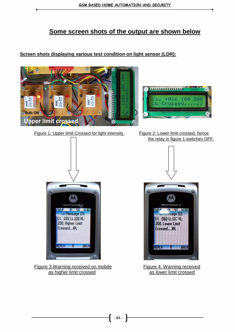
Some screen shots of the output are shown below
Screen shots displaying various test condition on light sensor (LDR):
Figure 1: Upper limit Crossed for light intensity. Figure 2: Lower limit crossed; hence
the relay in figure 1 switches OFF.
Figure 3 Warning received on mobile Figure 4: Warning received as higher limit crossed as lower limit crossed

GSM BASED HOME AUTOMATION AND SECURITY
- 85 -
Screen shots displaying various test condition on Temperature sensor (LM35):
Figure 5: Upper limit Crossed for Temperature and cooler Figure 6: Lower limit Crossed
Turns ON for Temperature and heater
turns ON
Figure 3: Warning received on mobile Figure 4: Warning received
higher limit crossed as lower limit crossed

GSM BASED HOME AUTOMATION AND SECURITY
- 86 -
Testing Anti-Theft Feature:
Figure 8: Type correct password to get access Figure 9: On typing correct password
Figure 10: Type correct password to get access Figure 11: On typing incorrect password
Figure 12: Type correct password to get access Figure 13: On typing incorrect password
Figure 14: Warning on cell phone after 3 wrong attempts

GSM BASED HOME AUTOMATION AND SECURITY
- 87 -
Testing smoke detector:
Figure 14: On detecting smoke
Figure 15: Warning on detection of
Smoke

GSM BASED HOME AUTOMATION AND SECURITY
- 88 -
Appendix
Layouts:
Layout of Microcontroller
Track side of P89C51 PCB Layout Component side P89C51PCB
Layout of ADC 0809
Track side of ADC 0809 PCB Layout Component side ADC 0809 PCB
GSM BASED HOME AUTOMATION AND SECURITY
- 89 -
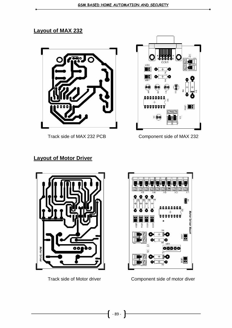
Layout of MAX 232
Track side of MAX 232 PCB Component side of MAX 232
Layout of Motor Driver
Track side of Motor driver Component side of motor diver

GSM BASED HOME AUTOMATION AND SECURITY
- 90 -
Layout of Power Supply
Track side of Power supply Component side of Power supply
L293DL293DD
PUSH-PULL FOUR CHANNEL DRIVER WITH DIODES
600mA OUTPUT CURRENT CAPABILITYPER CHANNEL 1.2A PEAK OUTPUT CURRENT (non repeti-tive) PER CHANNELENABLE FACILITY OVERTEMPERATURE PROTECTION LOGICAL "0" INPUT VOLTAGE UP TO 1.5 V(HIGH NOISE IMMUNITY)INTERNAL CLAMP DIODES
DESCRIPTIONThe Device is a monolithic integrated high volt-age, high current four channel driver designed toaccept standard DTL or TTL logic levels and driveinductive loads (such as relays solenoides, DCand stepping motors) and switching power tran-sistors.To simplify use as two bridges each pair of chan-nels is equipped with an enable input. A separatesupply input is provided for the logic, allowing op-eration at a lower voltage and internal clamp di-odes are included.This device is suitable for use in switching appli-cations at frequencies up to 5 kHz.
The L293D is assembled in a 16 lead plasticpackaage which has 4 center pins connected to-gether and used for heatsinkingThe L293DD is assembled in a 20 lead surfacemount which has 8 center pins connected to-gether and used for heatsinking.
July 2003
®
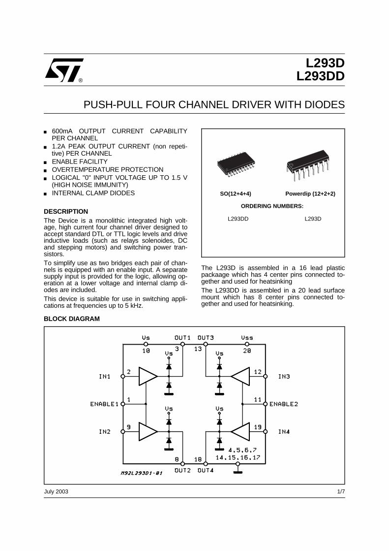
BLOCK DIAGRAM
SO(12+4+4) Powerdip (12+2+2)
ORDERING NUMBERS:
L293DD L293D
1/7

ABSOLUTE MAXIMUM RATINGS
Symbol Parameter Value Unit
VS Supply Voltage 36 V
VSS Logic Supply Voltage 36 V
Vi Input Voltage 7 V
Ven Enable Voltage 7 V
Io Peak Output Current (100 µs non repetitive) 1.2 A
Ptot Total Power Dissipation at Tpins = 90 °C 4 W
Tstg, Tj Storage and Junction Temperature – 40 to 150 °C
THERMAL DATA
Symbol Decription DIP SO Unit
Rth j-pins Thermal Resistance Junction-pins max. – 14 °C/W
Rth j-amb Thermal Resistance junction-ambient max. 80 50 (*) °C/W
Rth j-case Thermal Resistance Junction-case max. 14 –
(*) With 6sq. cm on board heatsink.
PIN CONNECTIONS (Top view)
SO(12+4+4) Powerdip(12+2+2)
L293D - L293DD
2/7

ELECTRICAL CHARACTERISTICS (for each channel, VS = 24 V, VSS = 5 V, Tamb = 25 °C, unlessotherwise specified)
Symbol Parameter Test Conditions Min. Typ. Max. Unit
VS Supply Voltage (pin 10) VSS 36 V
VSS Logic Supply Voltage (pin 20) 4.5 36 V
IS Total Quiescent Supply Current(pin 10)
Vi = L ; IO = 0 ; Ven = H 2 6 mA
Vi = H ; IO = 0 ; Ven = H 16 24 mA
Ven = L 4 mA
ISS Total Quiescent Logic SupplyCurrent (pin 20)
Vi = L ; IO = 0 ; Ven = H 44 60 mA
Vi = H ; IO = 0 ; Ven = H 16 22 mA
Ven = L 16 24 mA
VIL Input Low Voltage (pin 2, 9, 12,19)
– 0.3 1.5 V
VIH Input High Voltage (pin 2, 9,12, 19)
VSS ≤ 7 V 2.3 VSS V
VSS > 7 V 2.3 7 V
IIL Low Voltage Input Current (pin2, 9, 12, 19)
VIL = 1.5 V – 10 µA
IIH High Voltage Input Current (pin2, 9, 12, 19)
2.3 V ≤ VIH ≤ VSS – 0.6 V 30 100 µA
Ven L Enable Low Voltage(pin 1, 11)
– 0.3 1.5 V
Ven H Enable High Voltage(pin 1, 11)
VSS ≤ 7 V 2.3 VSS V
VSS > 7 V 2.3 7 V
Ien L Low Voltage Enable Current(pin 1, 11)
Ven L = 1.5 V – 30 – 100 µA
Ien H High Voltage Enable Current(pin 1, 11)
2.3 V ≤ Ven H ≤ VSS – 0.6 V ± 10 µA
VCE(sat)H Source Output SaturationVoltage (pins 3, 8, 13, 18)
IO = – 0.6 A 1.4 1.8 V
VCE(sat)L Sink Output Saturation Voltage(pins 3, 8, 13, 18)
IO = + 0.6 A 1.2 1.8 V
VF Clamp Diode Forward Voltage IO = 600nA 1.3 V
tr Rise Time (*) 0.1 to 0.9 VO 250 ns
tf Fall Time (*) 0.9 to 0.1 VO 250 ns
ton Turn-on Delay (*) 0.5 Vi to 0.5 VO 750 ns
toff Turn-off Delay (*) 0.5 Vi to 0.5 VO 200 ns
(*) See fig. 1.
L293D - L293DD
3/7

TRUTH TABLE (one channel)
Input Enable (*) Output
HLHL
HHLL
HLZZ
Z = High output impedance(*) Relative to the considered channel
Figure 1: Switching Times
Figure 2: Junction to ambient thermal resistance vs. area on board heatsink (SO12+4+4 package)
L293D - L293DD
4/7

DIM.mm inch
MIN. TYP. MAX. MIN. TYP. MAX.
a1 0.51 0.020
B 0.85 1.40 0.033 0.055
b 0.50 0.020
b1 0.38 0.50 0.015 0.020
D 20.0 0.787
E 8.80 0.346
e 2.54 0.100
e3 17.78 0.700
F 7.10 0.280
I 5.10 0.201
L 3.30 0.130
Z 1.27 0.050Powerdip 16
OUTLINE ANDMECHANICAL DATA
L293D - L293DD
5/7

1 10
1120
A
eB
D
E
L
K
H
A1 C
SO20MEC
h x 45˚
SO20
DIM.mm inch
MIN. TYP. MAX. MIN. TYP. MAX.
A 2.35 2.65 0.093 0.104
A1 0.1 0.3 0.004 0.012
B 0.33 0.51 0.013 0.020
C 0.23 0.32 0.009 0.013
D 12.6 13 0.496 0.512
E 7.4 7.6 0.291 0.299
e 1.27 0.050
H 10 10.65 0.394 0.419
h 0.25 0.75 0.010 0.030
L 0.4 1.27 0.016 0.050
K 0 ̊(min.)8 ̊(max.)
OUTLINE ANDMECHANICAL DATA
L293D - L293DD
6/7

Information furnished is believed to be accurate and reliable. However, STMicroelectronics assumes no responsibility for the consequencesof use of such information nor for any infringement of patents or other rights of third parties which may result from its use. No license isgranted by implication or otherwise under any patent or patent rights of STMicroelectronics. Specification mentioned in this publication aresubject to change without notice. This publication supersedes and replaces all information previously supplied. STMicroelectronics productsare not authorized for use as critical components in life support devices or systems without express written approval of STMicroelectronics.
The ST logo is a registered trademark of STMicroelectronics© 2003 STMicroelectronics – Printed in Italy – All Rights Reserved
STMicroelectronics GROUP OF COMPANIESAustralia - Brazil - Canada - China - Finland - France - Germany - Hong Kong - India - Israel - Italy - Japan - Malaysia - Malta - Morocco -
Singapore - Spain - Sweden - Switzerland - United Kingdom - United States.http://www.st.com
L293D - L293DD
7/7


Bibliography
Books
The 8051 Microcontroller and Embedded Systems, ’Muhammad Ali Mazidi,
Janice Gillespie Mazidi ’, 4th Reprint 2002, Pearson Education Inc. Pg 184-193,236-243
The 8051 Microcontroller Architecture, Programming and Applications,
‘Kenneth J. Ayala’, 2nd Edition, Delinar Publishers Inc. Pg 134-136, 155, 185-197. Websites GSM:
http://www.m-indya.com/gsm/gsmarchitecture.php http://www.roggeweck.net/uploads/media/Student_-_GSM_Architecture.pdf (Referred on 14-4-09) LDR: http://en.wikipedia.org/wiki/Photoresistor (Referred on 08-04-09) LM35: http://www.national.com/appinfo/tempsensors/files/temphb.pdf http://www.ece.osu.edu/~passino/LM35.pdf (Referred on 08-04-09) Microcontroller:
http://www.8051projects.info/tutorials.asp (Referred on 4-4-09) SIM:
http://en.wikipedia.org/wiki/Subscriber_Identity_Module (Referred on 14-4-09) Smoke Sensor:
http://en.wikipedia.org/wiki/Smoke_detector (Referred on 14-04-09) F-bus communication:
http://www.embedtronics.com/nokia/fbus.html (Referred on 4-4-09) L293D
http://www.triindia.co.in/resources/?p=54 (Referred on 4-4-09)