Embed Size (px)
Citation preview
University of Groningen
Semiconducting SWNTs sorted by polymer wrappingDerenskyi, Vladimir; Gomulya, Widianta; Gao, Jia; Bisri, Satria Zulkarnaen; Pasini,Mariacecilia; Loo, Yueh-Lin; Loi, MariaPublished in:Journal of Materials Research
DOI:10.1063/1.5011388
IMPORTANT NOTE: You are advised to consult the publisher's version (publisher's PDF) if you wish to cite fromit. Please check the document version below.
Document VersionFinal author's version (accepted by publisher, after peer review)
Publication date:2018
Link to publication in University of Groningen/UMCG research database
Citation for published version (APA):Derenskyi, V., Gomulya, W., Gao, J., Bisri, S. Z., Pasini, M., Loo, Y-L., & Loi, M. A. (2018). SemiconductingSWNTs sorted by polymer wrapping: How pure are they? Journal of Materials Research, 112(7), [072106].DOI: 10.1063/1.5011388
CopyrightOther than for strictly personal use, it is not permitted to download or to forward/distribute the text or part of it without the consent of theauthor(s) and/or copyright holder(s), unless the work is under an open content license (like Creative Commons).
Take-down policyIf you believe that this document breaches copyright please contact us providing details, and we will remove access to the work immediatelyand investigate your claim.
Downloaded from the University of Groningen/UMCG research database (Pure): http://www.rug.nl/research/portal. For technical reasons thenumber of authors shown on this cover page is limited to 10 maximum.
Download date: 18-03-2018
1
Semiconducting SWNTs sorted by polymer wrapping – How pure are they?
Vladimir Derenskyi1, Widianta Gomulya1,3, Jia Gao2, Satria Zulkarnaen Bisri1,3, Mariacecilia Pasini4, Yueh-Lin Loo2,5, Maria Antonietta Loi1*
1 Zernike Institute for Advanced Materials, University of Groningen, Nijenborgh 4, Groningen 9747 AG, The Netherlands E-mail: [email protected] 2 Department of Chemical and Biological Engineering, Princeton University, Princeton, New Jersey 08544, United States 3 RIKEN Center for Emergent Matter Science (CEMS), 2-1 Hirosawa, Wako-shi, Saitama, 351-0198, Japan 4 Istituto per lo Studio delle Macromolecole (CNR), Via A. Corti 12, 20133 Milano, Italy 5 Andlinger Center for Energy and the Environment, Princeton University, Princeton, NJ 08544, United States
ABSTRACT: Short-channel field-effect transistors (FETs) prepared from semiconducting
single-walled carbon nanotube (s-SWNT) dispersions sorted with poly(2,5-
dimethylidynenitrilo-3,4-didodecylthienylene) (PAMDD), are demonstrated. Electrical
analysis of the FETs show no evidence of metallic tubes out of a total number of 646 SWNTs
tested, implying an estimated purity of our semiconducting SWNT solution higher than
99.85%. These findings confirm the effectiveness of the polymer-wrapping technique in
selecting semiconducting SWNTs, as well as the potential of sorted nanotubes for the
fabrication of short channel FETs comprising from 1 to up to 15 nanotubes without inter-
nanotube junctions.
KEYWORDS: Semiconducting carbon nanotube, polymer-wrapping, field-effect transistor,
short channel
2
Single-walled carbon nanotubes (SWNTs) remain one of the strongest candidates for the
applications of high-performance nanoscale field-effect transistors (FETs). The one-
dimensional nature of SWNTs, and such properties as intrinsic ambipolarity1, high carrier
mobility2 and ballistic electron transport3 make them perfect building blocks for the
fabrication of transistors for high-speed, low-cost and low power-consumption electronics. In
order to utilize the full potential of SWNTs in FETs, however, a few challenges must be
overcome, including the separation of metallic (m-SWNT) and semiconducting (s-SWNT)
species present in the as-synthesized material. After a decade of extensive research in the field
of sorting s-SWNTs, post-growth purification techniques, such as column chromatography,4
dielectrophoresis,5 density gradient ultracentrifugation,6,7 weak field centrifugation,8 DNA9
and polymer-assisted SWNT separation10 have been successfully developed.
One of the most promising techniques for sorting s-SWNTs is the one using conjugated
polymers, which takes the advantage of the non-covalent interaction of the backbone and side
chains of certain conjugated polymers with SWNTs with specific structures10. This method
has significant advantages over other techniques, including the high purity of the sorted s-
SWNTs, minimal detrimental effect on their structure, ease of processing, high
reproducibility and scalability.11
Following the discovery of this method, polyfluorene-12 and polythiophene-based13
conjugated polymers with different side-chains14 have demonstrated excellent ability to select
semiconducting SWNTs based on their helicity and/or diameters. Indeed, s-SWNTs
dispersions prepared in this way have enabled the fabrication of high-performance SWNT
network-based FETs exhibiting high on/off current ratio modulation (up to 108)15, and charge
mobility above 30 cm2/ V·s.14,16 A trade-off between the extracted field-effect mobility and
current on/off ratio is generally observed, which has been ascribed to the presence of residual
metallic nanotubes in the carbon nanotube networks that work as FET channel. Due to the fact
3
that most FETs reported so far comprise device channel much longer than the average length
of the dispersed carbon nanotube, the FETs may still exhibit high current on/off ratios when
the metallic species are below the percolation threshold.17
Such observation cast doubts on the actual purity of polymer-sorted s-SWNTs, even though
spectroscopic characterization shows no detectable signals of m-SWNTs. For the ultimate
goal of building nanoscale logic circuit with s-SWNTs, a reliable evaluation of the
semiconductor purity of polymer-wrapped SWNTs is desirable.
Statistical analysis of the electrical performance of single-nanotube field-effect transistors is a
more reliable approach to evaluate the purity of s-SWNT dispersion compare to spectroscopic
methods. Recently, single-tube transistors based on s-SWNT dispersions prepared either with
column chromatography18 or polymer sorting19 have been demonstrated. In the polymer
sorting work, the purity of semiconducting SWNTs solutions sorted with polyfluorene was
estimated by evaluating the on/off ratios of transistors having a channel length of 240 nm
using arrays of SWNTs.19
Recently, we reported the high yield (16%) sorting of semiconducting SWNT by using the
polymer poly(2,5-dimethylidynenitrilo-3,4-didodecylthienylene) (PAMDD).16 Field-effect
transistors comprising such carbon nanotube networks exhibit mobilities above 30 cm2/Vs
and on/off ratio of 106.
In this article, we report the performance of field-effect transistors comprising individual
PAMDD-wrapped s-SWNT as the active channel. Field-effect transistors with channel length
of 300 nm, i.e., smaller than the average length of the SWNTs, were fabricated. On/off
current ratios as high as 105 for electron enhancement and 104 for hole enhancement regimes
were obtained. The distribution of the on current and of the threshold voltages displays high
stability over the 190 fabricated devices. Moreover, in none of the measured devices, short-
circuit was observed. Such a short-circuit would occur in short-channel SWNT-based FETs

4
only if metallic SWNT species would be present in the channel. Given the absence of short-
circuited devices, the statistical results indicate that the PAMDD-sorted s-SWNT dispersion
contains > 99.85% pure semiconducting species.
s-SWNTs were selected with a polyazomethine (PAMDD)16,20,21,22 polymer. The chemical
structure of PAMDD is shown in Figure 1(a). The polymer was synthesized through a
condensation reaction between 2,5-Diformyl-3,4-didodecylthiophene and p-
phenylenediamine. It is worthy to note that imine polymerization does not require any metal
catalysts typically used for traditional conjugated polymer synthesis. Moreover imine
chemistry seems to be very promising for the development of “green electronics” thanks to
the absence of noble metal catalysts and toxic phosphorous ligands, which allows a totally
disintegrable and biocompatible semiconducting polymer.23
The selection process consists of two main steps, ultrasonication and
ultracentrifugation24. Briefly, the ultrasonication process destroys nanotube bundles, allowing
the polymer to interact with the walls of SWNTs (Fig. 1(b)) and to disperse individual
nanotubes in organic solvents. During ultracentrifugation, the undispersed metallic nanotubes,
bundles and other forms of carbon present in the as-synthesized material precipitate and are
then removed. The excellent s-SWNT extraction yield (16%) obtained with PAMDD is
attributed to the presence of Nitrogen atoms in the polymeric backbone, which display a very
high affinity for the polarizable walls of SWNTs; details on this mechanism and attribution of
chirality and diameter of the SWNTs extracted, have been reported elsewhere16

5
Figure 1. (a) Chemical structure of the PAMDD polymer used for the selection of the
semiconducting SWNTs (b) schematic structure of a SWNT wrapped by a polymer chains (c)
absorption spectra of the enriched HiPCO-PAMDD nanotube solution.
The absorption spectrum of the HiPCO-PAMDD solution is shown in Fig. 1(c). Two
sets of sharp peaks in the ranges between 600 nm – 900 nm and 1000 nm – 1600 nm
corresponding to the second (S22) and the first (S11) electronic transitions of s-SWNTs,
respectively, are observed. The first electronic transitions of metallic nanotubes, M11, usually
appear in the range between 400 nm and 600 nm. However, the broad absorption peak of
PAMDD in this same range masks any signature of metallic nanotubes, even if they were
present. This spectral overlap thus precludes the quantification of the purity of s-SWNTs by
absorption spectroscopy.
Even though FETs with high mobility and current on/off ratio based on this dispersion
have been demonstrated,16 we did not previously quantify the purity of semiconducting
SWNTs. Being the extraction yield of this polymer one of the highest is important to quantify

6
the number of metallic tubes, as very often the effectiveness in selecting semiconducting
tubes is inversely proportional to yield. Herein, we then adopt an alternative method of
evaluating the purity of s-SWNTs in the HiPCO-PAMDD solution by analyzing the charge-
transport characteristics of the short-channel FETs, i.e., of devices with source-drain distance
shorter than the average length of s-SWNTs (approx.1 µm)24.
Figure 2(a) shows the optical micrograph of the fabricated devices with a central
source electrode and 12 surrounding drain electrodes. The channel region of one such device
is illustrated in Fig. 2(b). The channel length is as short as 300 nm; this length was chosen to
avoid the formation of a SWNT network with nanotube-nanotube junctions within the
transistor channel. In addition, the 300-nm channel width minimizes the probability of
multiple SWNTs assembled in the channel region. Using this configuration, we were able to
study the performance of devices based on single or few s-SWNT bridging the source and
drain electrodes.

7
Figure 2. (a) Optical image of the fabricated FETs, one substrate includes 12 FETs with
common source electrode in the center and drain electrodes at the edges. (b) Schematic
structure of the single SWNT device. (c) AFM image of the source and drain electrodes
forming the FET channel together with an individual SWNT. The channel width and length
are 300 nm.
Two sets of SWNT FETs were fabricated for this experiment. HiPCO-PAMDD
solutions with different s-SWNT concentrations were spin-coated on top of highly-doped Si
wafer with thermally grown SiO2. Top Ti/Au source and drain electrodes were subsequently
defined by electron-beam lithography (Raith e-Line with a spatial resolution of 6 nm). The
experiment was repeated three times for each solution concentration for a total 150 and 40
fabricated devices with the low and the high concentration solutions, respectively. Figure 2(c)
displays the atomic force microscopy (AFM) micrograph of a FET with an individual
PAMDD-wrapped s-SWNT deposited between the electrodes, this sample was obtained with
the low concentration solution. The white spots on the image are most probably due to
residual PAMDD from the selection process and/or from incomplete removal of photoresist
during the lithographic step.
The drain (𝑉!) and the gate (𝑉!) voltage dependences of the drain current are shown
on Figure 3(a, b), respectively. Of 150 s-SWNT transistors measured, 46 exhibited
semiconducting behavior and 104 FETs showed no drain current, due to the absence of
nanotubes between the electrodes. This was verified by performing detailed AFM imaging in
the channels of these devices. The relatively low yield of functional devices (31 %) is
primarily due to the low probability of matching the randomly distributed SWNTs on the
substrate with the top electrodes.
8
Because of the bottom-gate structure with conventional SiO2 as gate dielectric, the
devices were operated up to 60 V. Fig. 3(a) shows the 𝐼! − 𝑉! output characteristic of a single
SWNT device; due to short-channel effects and the presence of contact resistance, the output
characteristics does not saturate as one would have predicted. The devices are ambipolar with
the maximum hole current of about 0.2 µA and electron current around 25 nA. The
transconductance curves showing values up to 8 nS are reported in the inset Fig. 3(c). These
values are comparable with previously reported results on FETs made with a few polymer-
wrapped SWNTs per channel25, but because of the SiO2 gate dielectric they do not compete
with the best devices reported recently using poly[(9,9-dioctylfluorenyl-2,7-diyl)-alt-co-(6,60-
(2,20-bipyridine))] (PFO-BPy) wrapped SWNTs.26 The current in the off-state (Fig. 3(b)) was
as low as 5 pA and was limited by the resolution of the measurement set-up. The measured
on- and off-currents in working transistors resulted in an average on/off ratio of 105 (Fig.
3(b)). Despite being limited by the applied drain voltage, these on/off ratio values are very
high and comparable with the highest reported on/off ratios for solution-processed SWNT
FETs with short transistor channels25.

9
Figure 3. Electrical measurements of a single SWNT FET. (a) output 𝐼! − 𝑉! demonstrates
gate-effect for 𝑉! varying between 0 and 50 V (-50 V) with steps of 10 V (-10 V) (b) transfer
𝐼! − 𝑉! characteristics for p- and n-type channels measured in linear operational regime
at 𝑉! = 0.4 𝑉. Drain current (𝐼!, black curve) and Gate current (𝐼! , red curve) (c) transfer
𝐼! − 𝑉! characteristics in linear scale. Insets: Transconductance plot for single SWNT FET.
10
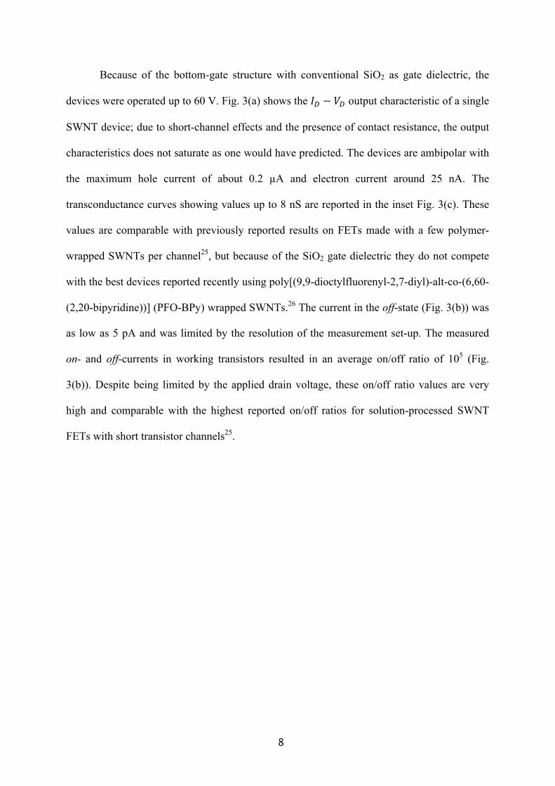
Unlike previous reports,27 showing that SWNT FETs with Ti/Au electrodes usually
display unipolar p-type characteristics when fabricated in ambient conditions due to the
trapping of electrons by adsorbed oxygen molecules28, our devices show ambipolar electrical
behavior even though the device fabrication was also performed in ambient conditions. This
recovery in ambipolarity likely stems from post-deposition annealing of the transistors,
carried out at 200⁰C in nitrogen atmosphere for 2 h, which allows the desorption of oxygen
and water molecules 29–31 and reestablishes the intrinsic charge transport properties.
Figure 4. (a) AFM image of the channel region. (b) output characteristics ( 𝑉! = 0.4 𝑉) of
FETs with few SWNTs crossing the channel. Hole current in this FET demonstrates a 25
times increase compared to that in a single SWNT FET. (c) Statistics of the threshold voltages
for hole and electron currents. (d) Linear scale of the transfer 𝐼! − 𝑉! characteristics for p-
and n-type channels measured at 𝑉! = 0.4 𝑉. Insets: Transfer characteristic in the hole-only
11
regime in logarithmic scale (left) and transconductance in the hole only regime plot for
multiple SWNT FET (right).
To further understand the uniformity of the electrical properties of PAMDD-sorted s-
SWNTs, we fabricated devices starting from a more concentrated solution. Figure 4(a) shows
an AFM micrograph showing one of these transistors with several SWNTs between the
electrodes. Fig. 4(b, d) display representative 𝐼! − 𝑉! (output) and 𝐼! − 𝑉! (transfer)
characteristics, respectively, obtained in a device comprising 10-15 s-SWNTs. The transistors
show higher hole current, about 12 µA at 𝑉! = −50 𝑉 and 𝑉! = −2 𝑉, and the electron
current (for 𝑉! = 50 𝑉 and 𝑉! = 2 𝑉) is about 200 nA compare to those based on individual
nanotubes (shown in Fig. 3). The current appears to scale approximately with the number of
the s-SWNTs bridging the channel, indicating that each nanotube, regardless of chirality (few
chiralities are present in the starting solution (see Fig. 1(c)), carries similar current under the
same conditions. Such uniformity is desirable for the integration of SWNT-based FETs into
arrays and circuits. Figure 4 (c) shows also the stability of the threshold shift over all the
single nanotube devices.
Figure 4 (d) shows the transfer characteristics in linear regime. That the current on/off
ratio values reaches more than 105 proves that all tubes within the channels are
12
semiconducting. The inset Fig. 4(d) shows the conductance of the same device.
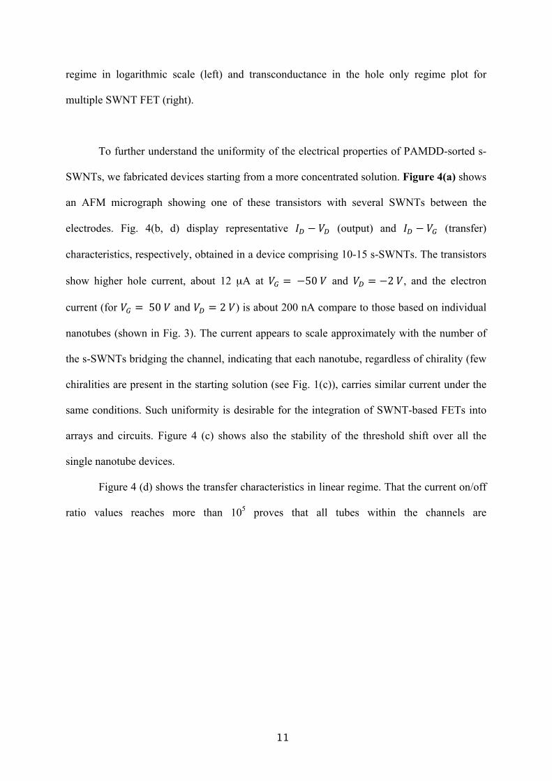
Figure 5. Diagram representing the distribution of on/off ratio in 150 FETs measured with
single SWNT in the channel region. 69% of fabricated devices did not show any current due
to the absence of SWNTs in channels. Working FETs demonstrated average on/off current
ratio 105.
The diagram reported in Figure 5 represents the statistical distribution of the on/off
ratio of the fabricated transistors. 80% of working devices demonstrate an average on/off
current ratio of 105 only about 9% show on/off between 104 and 103. Interestingly, of the 150
devices with single nanotubes and of the 40 devices with multiple tubes (an average of 15
tubes per device), for a total of 646 SWNTs measured, none of them failed short circuit.
Therefore from these data we can estimate that the percentage of metallic tubes in our
samples is lower that 0.15%, corresponding to a purity of semiconducting carbon nanotube
solution > 99.85%. This value is an underestimate; since no short-circuits where detected, to
precisely determine the purity of this high quality sample a much larger number of devices
would be required to precisely determine the purity of our s-SWNTs.
13
We have demonstrated statistical analysis on single-SWNT FETs prepared from a
PAMDD-wrapped s-SWNT solutions. Of 46 working single s-SWNT FETs and 40 multiple
tubes (avg. 15 tubes) FETs, an average on/off current ratio of 105 is observed. No traces of
metallic SWNTs were found in any of the prepared FETs (646 SWNTs tested), indicating an
estimated purity of our semiconducting SWNT solution higher than 99.85%. Statistical
analysis of the electrical conductance of s-SWNTs and of the threshold voltage (15%
variation) of SWNT-based FETs suggests rather uniform electrical characteristics of dispersed
s-SWNT. These findings confirm the effectiveness of the PAMDD in selecting
semiconducting SWNTs, as well as the potential of the sorted nanotubes for short-channel
FETs application.
Acknowledgements
The technical support of Arjen Kamp and Johan Holstein is acknowledged. The
Groningen team would like to thank the Stichting voor de Technische Wetenschappen (STW,
Utrecht, the Netherlands) for financial support. We would like also to thank Mario Caironi for
discussions.
See supplementary material for the detailed experimental section.
----------------------
References
1 S. Z. Bisri, C. Piliego, J. Gao, M. A. Loi, Adv. Mater., 26, 1176 (2014). 2 T. Dürkop, S. A. Getty, E. Cobas, M. S. Fuhrer, Nano Lett., 4, 35 (2004). 3 A. Javey, J. Guo, Q. Wang, M. Lundstrom, H. Dai, Nature, 424, 654 (2003). 4 H. Liu, D. Nishide, T. Tanaka, H. Kataura, Nat. Commun., 2, 309 (2011). 5 R. Krupke, F. Hennrich, H. V. Löhneysen, M. M. Kappes, Science, 301, 344 (2003). 6 M. S. Arnold, S. I. Stupp, M. C. Hersam, Nano Lett., 5, 713 (2005). 7 M. S. Arnold, A. A. Green, J. F. Hulvat, S. I. Stupp, M. C. Hersam, Nat. Nanotechnol., 1, 60
(2006). 8 W. G. Reis, R. T. Weitz, M. Kettner, A. Kraus, M. G. Schwab, Ž. Tomović, R. Krupke, J.
Mikhael, Sci. Rep., 6, 26259 (2016). 9 M. Zheng, A. Jagota, E. D. Semke, B. A. Diner, R. S. Mclean, S. R. Lustig, R. E.
Richardson, N. G. Tassi, Nat. Mater., 2, 338 (2003).

14
10 A. Nish, J. -Y. Hwang, J. Doig, R. J. Nicholas, Nat. Nanotechnol., 2, 640 (2007). 11 S. K. Samanta, M. Fritsch, U. Scherf, W. Gomulya, S. Z. Bisri, M. A. Loi, Acc. Chem.
Res., 47, 2446 (2014). 12 W. Gomulya, G. D. Costanzo, E. J. F. de Carvalho, S. Z.; Bisri, V. Derenskyi, M. Fritsch,
N. Fröhlich, S. Allard, P. Gordiichuk, A. Herrmann, S. J. Marrink, M. C. dos Santos, U. Scherf, M. A. Loi, Adv. Mater., 25, 2948 (2013).
13 H. W. Lee, Y. Yoon, S. Park, J. H. Oh, S. Hong, L. S. Liyanage, H. Wang, S. Morishita, N. Patil, Y. J. Park, J. J. Park, A. Spakowitz, G. Galli, F. Gygi, P. H. -S. Wong, J. B.-H. Tok, J. M. Kim, Z. Bao, Nat. Commun., 2, 541 (2011).
14 S. P. Schießl, N. Fröhlich, M. Held, F. Gannott, M. Schweiger, M. Forster, U. Scherf, J. Zaumseil, ACS Appl. Mater. Interfaces, 7, 682 (2015).
15 V. Derenskyi, W. Gomulya, J. M. Salazar-Rios, M. Fritsch, N. Fröhlich, S. Jung, S. Allard, S. Z. Bisri, P. Gordiichuk, A. Herrmann, U. Scherf, M. A. Loi, Adv. Mater., 26, 5969 (2014).
16 W. Gomulya, V. Derenskyi, E. Kozma, M. Pasini, M. A. Loi, Adv. Funct. Mater., 25, 5858 (2015).
17 C. Wang, J. Zhang, K. Ryu, A. Badmaev, L. G. De Arco, C. Zhou, Nano Lett., 9, 4285 (2009).
18 G. S. Tulevski, A. D. Franklin, A. Afzali, ACS Nano, 7, 2971 (2013). 19 G. J. Brady, Y. Joo, M. -Y. Wu, M. J. Shea, P. Gopalan, M. S. Arnold, ACS Nano, 8,
11614 (2014). 20 S. Destri, M. Pasini, C. Pelizzi, W. Porzio, G. Predieri, C. Vignali, Macromolecules, 32,
353 (1999). 21 T. Lei, X. Chen, G. Pitner, H.-S. P. Wong, and Z. Bao, J. Am. Chem. Soc. 138, 802 (2016). 22 T. Lei, I. Pochorovski, Z. Bao, Acc. Chem. Res., 50, 1096 (2017). 23 T. Lei, M. Guan, J. Liu, H. C. Lin, R. Pfattner, L. Shaw, A. F. McGuire, T. -C. Huang, L.
Shao, K. -T. Cheng, J. B. H. Tok, Z. Bao, Proceedings of the National Academy of Sciences, 114, 5107 (2017).
24 S. Z. Bisri, J. Gao, V. Derenskyi, W. Gomulya, I. Iezhokin, P. Gordiichuk, A. Herrmann, M. A. Loi, Adv. Mater., 24, 6147 (2012).
25 S. Park, H. W. Lee, H. Wang, S. Selvarasah, M. R. Dokmeci, Y. J. Park, S. N. Cha, J. M. Kim, Z. Bao, ACS Nano, 6, 2487 (2012).
26 G. J. Brady, A. J. Way, N. S. Safron, H. T. Evensen, P. Gopalan, M. S. Arnold, Science Adv., 2, e1601240 (2016).
27 A. Javey, H. Kim, M. Brink, Q. Wang, A. Ural, J. Guo, P. McIntyre, P. McEuen, M. Lundstrom, H. Dai, Nat. Mater., 1, 241 (2002).
28 V. Derycke, R. Martel, J. Appenzeller, P. Avouris, Appl. Phys. Lett., 80, 2773 (2002). 29 A. Javey, J. Guo, D. B. Farmer, Q. Wang, E. Yenilmez, R. G. Gordon, M. Lundstrom, H.
Dai, Nano Lett., 4, 1319 (2004). 30 S. J. Wind, J. Appenzeller, R. Martel, V. Derycke, P. Avouris, Appl. Phys. Lett., 80, 3817
(2002). 31 R. V. Seidel, A. P. Graham, J. Kretz, B. Rajasekharan, G. S. Duesberg, M. Liebau, E.
Unger, F. Kreupl, W. Hoenlein, Nano Lett., 5, 147 (2005).