Embed Size (px)
Citation preview
University of Groningen
Processing and structure of nanoparticlesDutka, Mikhail Vasilievich
IMPORTANT NOTE: You are advised to consult the publisher's version (publisher's PDF) if you wish to cite fromit. Please check the document version below.
Document VersionPublisher's PDF, also known as Version of record
Publication date:2014
Link to publication in University of Groningen/UMCG research database
Citation for published version (APA):Dutka, M. V. (2014). Processing and structure of nanoparticles: Characterization and modeling. [S.n.].
CopyrightOther than for strictly personal use, it is not permitted to download or to forward/distribute the text or part of it without the consent of theauthor(s) and/or copyright holder(s), unless the work is under an open content license (like Creative Commons).
The publication may also be distributed here under the terms of Article 25fa of the Dutch Copyright Act, indicated by the “Taverne” license.More information can be found on the University of Groningen website: https://www.rug.nl/library/open-access/self-archiving-pure/taverne-amendment.
Take-down policyIf you believe that this document breaches copyright please contact us providing details, and we will remove access to the work immediatelyand investigate your claim.
Downloaded from the University of Groningen/UMCG research database (Pure): http://www.rug.nl/research/portal. For technical reasons thenumber of authors shown on this cover page is limited to 10 maximum.
Download date: 05-04-2022
Chapter 3
3Characterization of nanoparticles
Chapter 3 summarizes the various experimental methods that have been
employed during this thesis work so as to characterize nanostructured materials.
The principal technique used is high resolution transmission electron microscopy. It
will be shown that the concepts of resolution in high-resolution transmission
electron microscopy (HRTEM) are still not without pitfalls, and a thorough
understanding of image formation is essential for a sound interpretation. High-
resolution TEM imaging is based on the same principles as introduced by Frits
Zernike for optical microscopy and phase contrast imaging in HRTEM derives
contrast from the phase differences among the different beams scattered by the
specimen, causing addition and subtraction of amplitude from the forward-scattered
beam. However, in reality a HRTEM is not a perfect phase contrast microscope and
electron beams at different angles with the optical axis obtain different phase shifts.
Besides HRTEM this chapter presents a concise introduction to scanning electron
microscopy and to the important issues of image processing and analysis of
nanostructured materials.
3.1 Introduction to electron microscopy
Electron Microscopy in the field of nanostructured materials is devoted to
linking structural observations to functional performance. In turn, the
microstructural features are determined by chemical composition and processing.
Unfortunately a straightforward correlation between structural information obtained
by electron microscopy and properties of nanostructured systems is still hampered
by fundamental and practical reasons. First, defects affecting the properties of
nanostructured systems are in fact not in thermodynamic equilibrium and their
behavior may be very much non-linear. Second, a quantitative evaluation of the
structure-property relationship can be rather difficult because of statistics.
Chapter 3
30
The wave-like characteristics of electrons that are essential for electron
microscopy were first postulated in 1924 by Louis de Broglie (in fact in his PhD
thesis [1] sic!, Nobel Prize in Physics in 1929), with a wavelength far less than
visible light. In the same period Busch revealed that an electromagnetic field might
act as a focusing lens on electrons [2]. Subsequently, the first electron microscope
was constructed in 1932 by Ernst Ruska. For his research, he was awarded, much
too late of course, in 1986 the Nobel Prize in Physics together with Gerd Binnig and
Heinrich Rohrer who invented the scanning tunneling microscope. The electron
microscope opened new horizons to visualize materials structures far below the
resolution reached in light microscopy. The most attractive point is that the
wavelength of electrons is much smaller than atoms and it is at least theoretically
possible to see details well below the atomic level.
However, currently it is impossible to build transmission electron microscopes
with a resolution limited by the electron wavelength, mainly because of
imperfections of the magnetic lenses. In the middle of the 70’s the last century
commercial TEMs became available that were capable of resolving individual
columns of atoms in crystalline materials. High voltage electron microscopes, i.e.
with accelerating voltages between 1 MV and 3 MV have the advantage of shorter
wavelength of the electrons, but a drawback is that also radiation damage increases.
After that period HRTEMs operating with intermediate voltages between 200 kV –
400 kV were designed offering very high resolution close to that achieved
previously in the ranging between 1 and 3 MV.
More recently, developments were seen to reconstruct the exit wave (from a
defocus series) and to improve the directly interpretable resolution to the
information limit. In fact during the last two decades, electron microscopy has
witnessed a number of innovations that enhanced existing approaches of exit wave
reconstruction and introduced qualitatively new techniques. One of the most
important novel technologies is aberration correction. Correction of spherical
aberration sC has been demonstrated by Haider et al. [3]. In the years that followed,
this hexapole corrector was applied to various materials science problems [4-6]. A
quadrupole/octopole corrector was developed and applied by Dellby et al. [7] for
scanning transmission electron microscopy (STEM) mode. Since then, aberration
correction has been used to help solve various material science problems [8-10].
Recently, correction of chromatic aberration has been demonstrated [11] and
successfully applied to improve resolution in energy-filtered TEM (EFTEM) by a
factor of five or so. Furthermore, there has been significant progress in EELS,
resulting in improved energy resolution (monochromator) and a larger field of view
Characterization of nanoparticles
31
for electron-spectroscopic [12] and energy-filtered imaging [13]. For a review
reference is made to [14].
Elastically scattered electrons provide the basics of the image formation in
HRTEM and they are the predominant fraction of the transmitted electrons for small
sample thickness (< 15 nm). In contrast, the thicker the sample the more electrons
become inelastically scattered and this must be prevented as much as possible,
because they contribute mostly to the background intensity of the image. Therefore,
the thinner the specimen (< 15 nm) the better the quality of the HRTEM images. The
inelastic scattered electrons can be removed by inserting an energy filter in the
microscope between specimen and recording device. In the following section on
image formation, only the elastic scattered electrons are considered. The main
technique for detailed examination of the structure of nanoparticles in our work
concerns transmission electron microscopy but also scanning electron microscopy
(SEM) has been employed.
Here we present a concise review of electron microscopy and other
nanoparticle characterization techniques for non-experts, without going into every
detail. This part is based on summaries that were also presented in several reviews
[15,16] and by former PhDs of our MK group, in particular by Bas Groen, Patricia
Carvalho, Wouter Soer, Zhenguo Chen, Sriram Venkatesan, Stefan Mogck and
Sergey Punzhin [17-23].
3.2 Transmission electron microscopy
A schematic picture of a TEM is shown in Figs. 3.1 and 3.2. A transmission
electron microscope consists of an illumination system, specimen stage and imaging
system, analogous to a conventional light microscope. Several textbooks and
reviews have been written on the subject of (high resolution) microscopy, sadly with
different notation conventions. This chapter adopts the notation used in [24,25].
Spence [26] has presented a more in-depth description of imaging in HRTEM
theory. Williams and Carter [27] have written a very inspirational and practical
textbook on general aspects of electron microscopy. In our work two different
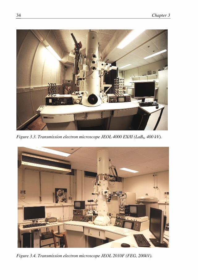
transmission electron microscopes were used, a JEOL 4000 EX/II (LaB6, 400 kV)
for atomic structure observations (Fig. 3.3) and a JEOL 2010F (FEG, 200kV) for
EDS analysis (Fig. 3.4). For a textbook on theory behind elastic and inelastic
scattering processes in TEM reference is also made to [28].
Chapter 3
32
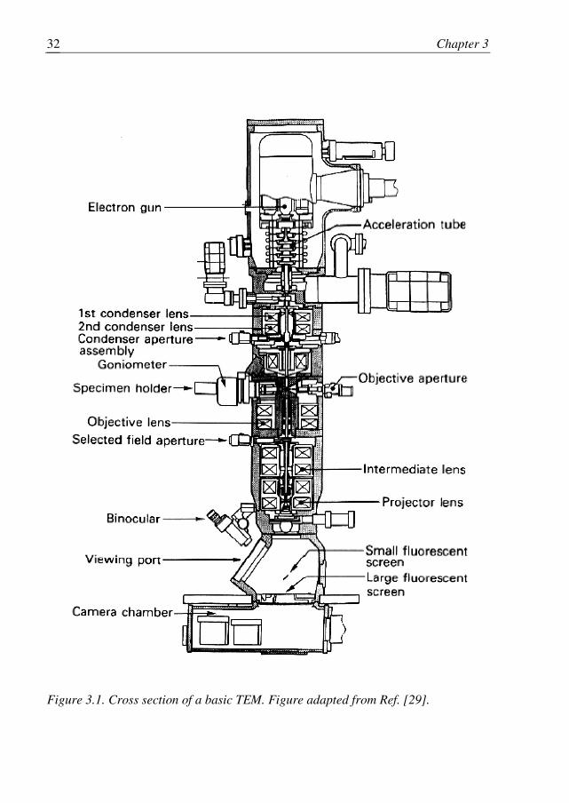
Figure 3.1. Cross section of a basic TEM. Figure adapted from Ref. [29].
Characterization of nanoparticles
33
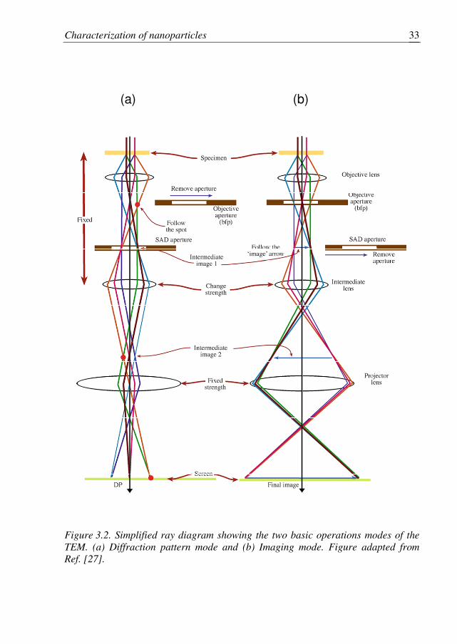
(a) (b)
Figure 3.2. Simplified ray diagram showing the two basic operations modes of the
TEM. (a) Diffraction pattern mode and (b) Imaging mode. Figure adapted from
Ref. [27].
Chapter 3
34
Figure 3.3. Transmission electron microscope JEOL 4000 EX/II (LaB6, 400 kV).
Figure 3.4. Transmission electron microscope JEOL 2010F (FEG, 200kV).
Characterization of nanoparticles
35
3.2.1 Illumination system
Electrons are generated in an electron gun, accelerated towards the anode and
focused at the specimen with condenser lenses. High resolution TEM requires planar
coherent electron waves, since high-resolution micrographs are formed by phase
contrast. For elemental analysis, it is also important to have the possibility to focus
the electron beam within a diameter (FWHM) of the order of 1 nm to determine
chemical compositions in the nanometer range. Several demands must be fulfilled:
high brightness, small source size and little energy spread of the electrons. The
brightness of the beam is an important parameter and is defined as follows
I
BA
=Ω
(3.1)
i.e. the brightness value B is related to the electron current I emitted from the area
A (which also determines the spatial coherency) into the spatial angle Ω . The
conventional way to generate electrons is to use thermionic emission. Any material
that is heated to a high enough temperature will emit electrons when they have
enough energy to overcome the work function. In practice this can only be done with
high melting materials (such as tungsten) or low work function materials like LaB6.
Richardson’s law describes thermionic emission as a function of the work function
W and temperature T
2 expW
J CTkT
= − (3.2)
with the current density J at the tip and C the so-called Richardson-Dushman's
constant depending on the material used for the tip. In electron microscopes tungsten
filaments were most commonly used until the introduction of LaB6. LaB6 sources
have the advantages of a lower operating temperature that reduces the energy spread
of the electrons and increases the brightness.
Another way of extracting electrons from a material is to apply a high electric
field to the emitter that enables the electrons to tunnel through the barrier.
Sharpening the tip may enhance the electric field since the electric field at the apex
of the tip is inversely proportional to the radius of the apex
V
EkR
= , (3.3)
with k a correction factor for the tip geometry (usually around 2). The advantage of
this cold field emitter gun (cold FEG) is that the emission process can be to done at
room temperature, reducing the energy spread of the electrons. The small size of the
emitting area and the shape of the electric field results in a very small (virtual)
Chapter 3
36
source size in the order of nanometers with a brightness that is three orders of
magnitude higher than for thermionic sources. It is thus possible to focus the beam
to a very small probe for chemical analysis at an atomistic level or to fan the beam to
produce a beam with high spatial coherence over a large area of the specimen. The
disadvantages of this type of emitter are the need for (expensive) UHV equipment to
keep the surface clean, the need for extra magnetic shielding around the emitter and
the limited lifetime. For electric fields E > 107 V/cm the electron current density J
can be described according the modified Fowler-Nordheim relation
6 7 3 2
22
1 54 10 6 8 10 /. . ( )exp
( )
v y WJ E
EWt y
− − × × = − ’ (3.4)
where J is the field-emitted current density in A/m2, E is the applied electric field at
the tip, and W is the work function in eV. The functions v and t of the variable
1 243 79 10.y E ϕ−= × depend weakly on the applied electric field and have been
tabulated in literature [30]. In our FEG-TEM it is therefore possible to focus the
beam to a very small probe for chemical analysis at a sub-nanometer range and
produce a beam with high spatial coherence over a large area of the specimen. The
small (virtual) source size reaches values for the brightness in the order of B = 1011
to 1014 Am-2sr-1 with an energy spread of 0.2 – 0.5 eV compared with ~109 Am-2sr-1
and an energy spread of 0.8 – 1 eV for thermionic emission.
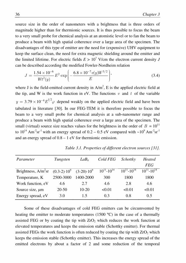
Table 3.1. Properties of different electron sources [31].
Parameter Tungsten LaB6 Cold FEG Schottky Heated
FEG
Brightness, A/m2sr (0.3-2)⋅109 (3-20)⋅109 1011-1014 1011-1014 1011-1014
Temperature, K 2500-3000 1400-2000 300 1800 1800
Work function, eV 4.6 2.7 4.6 2.8 4.6
Source size, µm 20-50 10-20 <0.01 <0.01 <0.01
Energy spread, eV 3.0 1.5 0.3 0.8 0.5
Some of these disadvantages of cold FEG emitters can be circumvented by
heating the emitter to moderate temperatures (1500 °C) in the case of a thermally
assisted FEG or by coating the tip with ZrO2 which reduces the work function at
elevated temperatures and keeps the emission stable (Schottky emitter). For thermal
assisted FEGs the work function is often reduced by coating the tip with ZrO2 which
keeps the emission stable (Schottky emitter). This increases the energy spread of the
emitted electrons by about a factor of 2 and some reduction of the temporal
Characterization of nanoparticles
37
coherency compared with cold FEGs. The Schottky emitter is widely used in
commercial FEG-TEMs, because of the stability, lifetime and high intensity.
Table 3.1 gives an overview of the technical data of different electron sources.
Transmission electron microscopes operate generally between 80 kV and
1000 kV meaning that the velocity of the electron includes relativistic effects (with
rest mass and energy, 0m and 0E , respectively. This must be taken into account
applying the De Broglie relationship to calculate the wavelength
1 2
00 0 2
0
2 12
/eE
h m eEm c
λ
− = + . (3.5)
For 400 kV electrons λ = 1.64 pm which is much smaller than the resolution
of any electron microscope because the resolution is limited by aberrations of the
objective lens and not by the wavelength of the electrons. The electron beam is now
focused on the specimen with the condenser lenses and aligned using several
alignment coils. The function of the condenser lens system is to provide a parallel
beam of electrons at the specimen surface. In practice this is not possible and the
beam always possesses a certain kind of convergence when imaging at high
resolution, usually in the range of 1 mrad for LaB6 emitters and 0.1 mrad for FEGs.
3.2.2 Interaction with specimen
After entering the specimen most of the electrons are scattered elastically by
the nuclei of the atoms in the specimen. Some electrons are inelastically scattered by
the electrons in the specimen. Compared to X-ray or neutron diffraction the
interaction of electrons with the specimen is huge and multiple scattering events are
common. For thick specimens at lower resolutions an incoherent particle model can
describe the interaction of the electrons with the specimen. However, with thin
specimens at high resolution this description fails because the wave character of the
electrons is then predominant. The electrons passing the specimen near the nuclei
are somewhat accelerated towards the nuclei causing small, local, reductions in
wavelength, resulting in a small phase change of the electrons. Information about the
specimen structure is therefore transferred to the phase of the electrons [14]. In the
following we take the convention for the wave description in solids which is
commonly used in crystallography. Spence [26] presents an interesting table listing
the differences, mainly in sign, between the Dirac notations and crystallography and
indeed one should be careful and aware of this when comparing different textbooks.
After the (plane) electron wave strikes the specimen a part of the electrons
experience a phase shift. The essential part of image formation in TEM is the
Chapter 3
38
transformation of the phase shift stored in the exit wave into amplitude modulation,
and therefore into visible contrast. With the assumption that the specimen is a pure
phase object the phase shift can be described with the exit plane function:
( )( ) exp ( )ep objectiϕ = − Φr r (3.6)
For sufficiently thin objects the phase of the object wave function can be considered
as weak 1( )objectΦ r ≪ and ( )epϕ r can be approximated to first order:
1( ) ( )ep objectiϕ = − Φr r . ( )objectΦ r is the projected potential distribution in the
materials slice, averaged over the electron beam direction. The technique of
HRTEM has a base in the technique of phase contrast microscopy, introduced by
Zernike [32] for optical microscopy in the physics department of our own university,
the University of Groningen. In 1953 he received the Nobel Prize in Physics for this
invention which made an undisputed immense impact, in particular into bio- and
medical sciences. The principle and very basic problem in any microscopy, both in
optical and electron microscopy, is to derive information about the object we are
interested in. The object is defined by amplitude and phase and to retrieve
information about ( )Φ r from the intensity of the image is a very complex because of
the so-called transfer function that takes ( )epϕ r into ( )imageϕ r . Even in an ideal but
non-existing (because of aberrations in any optical system in practice) microscope
the intensity of the image is exactly equal to the intensity of the object function but
unfortunately phase information is already lost in the intensity.
Zernike had a brilliant and at the same time an utmost simple idea – i.e. most
probably a prerequisite of any Nobel Prize. He realized that if the phase of the
diffracted beam can be shifted over 2/π it is as if the image function has the form
1( )
( )objecti
image objecte iϕ− Φ∝ ≅ − Φr
r and in fact neglecting any transfer function of
the microscope, the weak phase object acts as an amplitude object, i.e. the intensity
observed, i.e. 2
1 2( ) ( )image objectI ϕ= = + Φr r , can be connected to ( )objectΦ r .
High-resolution TEM imaging is based on the same principles. Phase-contrast
imaging derives contrast from the phase differences among the different beams
scattered by the specimen, causing addition and subtraction of amplitude from the
forward-scattered beam. Components of the phase difference come from both the
scattering processes itself and the electron optics of the microscope. Just because of
a fortunate balance between spherical aberration and defocus we can perform high-
resolution TEM with atomic resolution as will be shown in the following.
Characterization of nanoparticles
39
A possibility to visualize the phase contrast in TEM was introduced by
Scherzer. Perfect lenses do not show an amplitude modulation, but imaging
introduces an extra phase shift between the central beam and the beam further away
from the optical axis of the objective lens (deviation from the ideal Gaussian wave
front). Deviations from the ideal Gaussian wave front in lenses are known as
spherical aberration. For particular frequencies the phase contrast of the exit wave
will be nearly at optimum transferred into amplitude contrast. Therefore the
observed contrast in TEM micrographs is mainly controlled by the extra phase shift
of the spherical aberration and the defocus. The influence of the extra phase shift on
the image contrast can be taken into account by multiplying the wave function at the
back focal plane with the function describing the extra phase shift as a function of
the distance from the optical axis. The lenses can be conceived cylindrical
symmetric, and will be represented as a function of the distance of the reciprocal
lattice point to the optical axis ( )1 22 2U u v= + , where u and v are the angular
variables in reciprocal space. The extra phase factor ( )Uχ depends on the spherical
aberration and defocus [26]
2 3 40 5( ) . sU fU C Uχ πλ π λ= ∆ + (3.7)
with f∆ the defocus value and sC the spherical aberration coefficient. The function
that multiplies the exit wave is the so-called transfer function ( )Uξ
( ) ( )exp ( )U E U i Uξ χ = (3.8)
For the final image wave and intensity after the objective lens, assuming a weak
phase object with
21 2
( ) ( ) ( )
( ) ( ) ( ( ) ( )
image ep
image objectI
ϕ ϕ ξ
ϕ ξ
= ⊗
= = + Φ ⊗ ℑ
r r r
r r r r
(3.9)
where ℑ represents the Fourier transform. In fact the Fourier transform of the object
wave function is the electron diffractogram in the back focal plane of the objective
lens. As said before because of a fortunate balance between spherical aberration and
defocus, i.e. with the transfer function ( )ξ r in Eq. 2.9 going close to unity,
information about the object can be obtained from the image. After the
multiplication of Eq. (3.9) with its complex conjugate and neglecting the terms of
second order and higher the image formation results in
11 2( ) ( ) [ ( )sin( ( ))]imageI E U Uχ−= + Φ ⊗ ℑr r (3.10)
Chapter 3
40
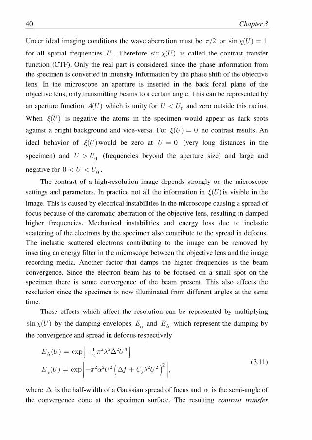
Under ideal imaging conditions the wave aberration must be 2/π or 1sin ( )Uχ = for all spatial frequencies U . Therefore sin ( )Uχ is called the contrast transfer
function (CTF). Only the real part is considered since the phase information from
the specimen is converted in intensity information by the phase shift of the objective
lens. In the microscope an aperture is inserted in the back focal plane of the
objective lens, only transmitting beams to a certain angle. This can be represented by
an aperture function ( )AU which is unity for 0U U< and zero outside this radius.
When ( )Uξ is negative the atoms in the specimen would appear as dark spots
against a bright background and vice-versa. For 0( )Uξ = no contrast results. An
ideal behavior of ( )Uξ would be zero at 0U = (very long distances in the
specimen) and 0U U> (frequencies beyond the aperture size) and large and
negative for 00 U U< < .
The contrast of a high-resolution image depends strongly on the microscope
settings and parameters. In practice not all the information in ( )Uξ is visible in the
image. This is caused by electrical instabilities in the microscope causing a spread of
focus because of the chromatic aberration of the objective lens, resulting in damped
higher frequencies. Mechanical instabilities and energy loss due to inelastic
scattering of the electrons by the specimen also contribute to the spread in defocus.
The inelastic scattered electrons contributing to the image can be removed by
inserting an energy filter in the microscope between the objective lens and the image
recording media. Another factor that damps the higher frequencies is the beam
convergence. Since the electron beam has to be focused on a small spot on the
specimen there is some convergence of the beam present. This also affects the
resolution since the specimen is now illuminated from different angles at the same
time.
These effects which affect the resolution can be represented by multiplying
sin ( )Uχ by the damping envelopes Eα and E∆ which represent the damping by
the convergence and spread in defocus respectively
( )
2 2 2 412
22 2 2 2 2
( ) exp
( ) exp ,s
E U U
E U U f C Uα
π λ
π α λ
∆ = − ∆
= − ∆ +
(3.11)
where ∆ is the half-width of a Gaussian spread of focus and α is the semi-angle of
the convergence cone at the specimen surface. The resulting contrast transfer
Characterization of nanoparticles
41
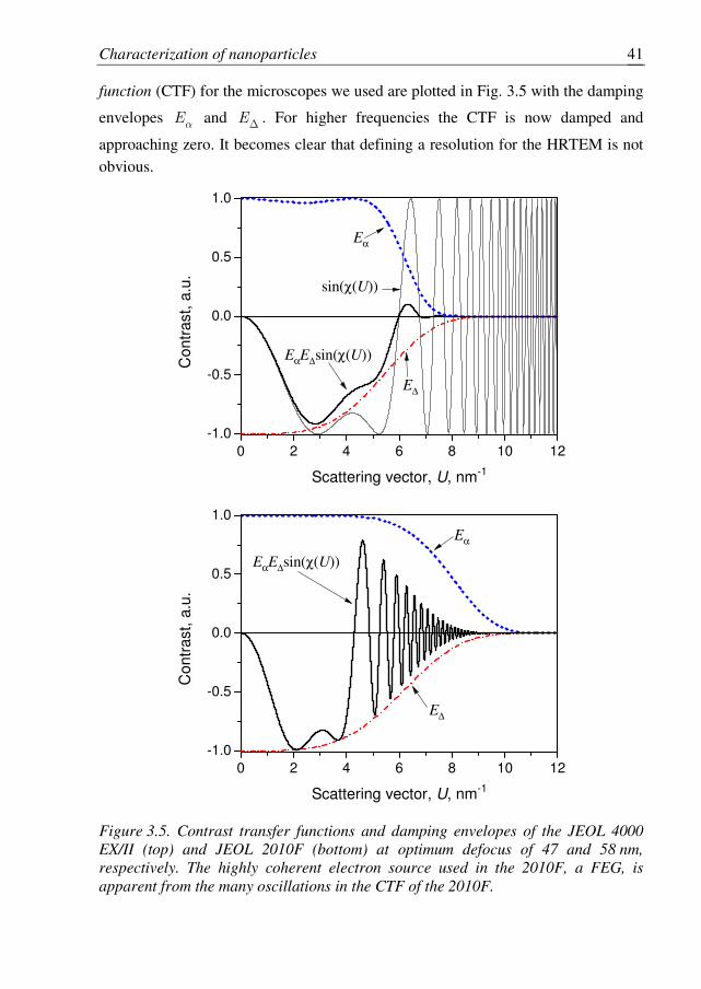
function (CTF) for the microscopes we used are plotted in Fig. 3.5 with the damping
envelopes Eα and E∆ . For higher frequencies the CTF is now damped and
approaching zero. It becomes clear that defining a resolution for the HRTEM is not
obvious.
0 2 4 6 8 10 12
-1.0
-0.5
0.0
0.5
1.0
Eα
E∆
sin(χ(U))
Contr
ast,
a.u
.
Scattering vector, U, nm-1
EαE∆sin(χ(U))
0 2 4 6 8 10 12
-1.0
-0.5
0.0
0.5
1.0
Contr
ast,
a.u
.
Scattering vector, U, nm-1
Eα
E∆
EαE∆sin(χ(U))
Figure 3.5. Contrast transfer functions and damping envelopes of the JEOL 4000
EX/II (top) and JEOL 2010F (bottom) at optimum defocus of 47 and 58 nm,
respectively. The highly coherent electron source used in the 2010F, a FEG, is
apparent from the many oscillations in the CTF of the 2010F.
Chapter 3
42
Several different resolutions can be defined as stated by O’Keefe [33]:
(1) Fringe or lattice resolution. This is related to the highest spatial frequency
present in the image. In thicker crystals second-order or non-linear interference
may cause this. Since the sign of sin ( )Uχ is not known there is in general no
correspondence between the structure and the image. This resolution is limited
by the beam convergence and the spread in defocus.
(2) Information limit resolution. This is related to the highest spatial frequency
that is transferred linearly to the intensity spectrum. These frequencies may fall
in a passband, with blocked lower frequencies. Usually this resolution is almost
equal to the lattice resolution. A definition used is that the information limit is
defined as the frequency where the overall value of the damping envelopes
corresponds to 2e− (e.g. the damping is 5% of the CTF intensity).
(3) Point resolution. This is the definition of the first zero point in the contrast
transfer function, right hand side of the Scherzer band. For higher spatial
frequencies, the image contrast and thus the structure cannot be unambiguously
interpreted. The optimal transmitted phase contrast is defined as a Scherzer
defocus: ( )1 24 3
/
sC λ and the highest transferred frequency is equal to
1 4 3 41 5 /. sC λ− − .
In Fig. 3.5 the CTFs of the JEOL 4000EX and JEOL 2010F at optimum
defocus are plotted with the damping envelopes. The corresponding electrical-
optical properties are listed in Table 3.2.
Table 3.2. Technical data of the used microscopes.
Parameter JEOL 4000EX/II JEOL 2010F
Emission LaB6 (filament)
FEG (Schottky emitter)
Operating voltage, 0E , kV 400 200
Spherical aberration coefficient, sC , mm 0.97 1.0
Spread of defocus, ∆ , nm 7.8 4.0
Beam convergence angle, α , mrad 0.8 0.1
Optimum defocus, f∆ , nm –47 –58
Information limit, nm 0.14 0.11
Point resolution, nm 0.165 0.23
Characterization of nanoparticles
43
For the two microscopes in the MK group with a different illumination system, it is
clearly visible that with the JEOL 2010F a rapid oscillation of the CTF occurs.
These oscillations arise because the spatial coherence is higher for the 2010F (spread
of defocus and in particular beam convergence is smaller) than for the 4000 EX/II.
Correspondingly, the information limit of the JEOL 2010F is better than of the
4000EX/II. For the JEOL 2010F the information limit is a factor 2 higher compared
with the point resolution. For microscopes with higher operating voltages, a FEG
will not significantly increase the information limit, because the higher the voltage
the larger the energy spread of the electrons and the damping envelope is limited by
the spread of defocus, instead of beam convergence. For lower (≤ 200 kV) voltage
TEMs the situation is clearly more favorable and a FEG thus significantly improves
the information limit. With higher voltage instruments the higher acceleration
voltage increases the brightness of the source and the damping envelope is limited
by the spread of defocus. The spherical aberration of the objective lens can be
lowered but generally at the expense of a decrease in tilt capabilities of the
specimen. It is possible to compensate sC by a set of hexapole lenses as suggested
by Scherzer [34] in 1947 but it was only feasible recently due to the complex
technology involved. Haider demonstrated a sC corrected 200 kV FEG microscope
[35] in which sC was set at 0.05 mm to reach an optimum between contrast and
resolution. The point resolution of this microscope was now equal to the information
limit of 0.14 nm. Successful application of this technology would put the limiting
factors of the microscope at the chromatic aberration and mechanical vibrations that
currently limit the resolution around 0.1 nm.
For a correct interpretation of the structure the specimen has to be carefully
aligned along a zone axis, which is done with the help of Kikuchi patterns and an
even distribution of the spot intensities in diffraction. The misalignment of the
crystal is in this way reduced to a fraction of a mrad. Beam tilt has a more severe
influence on the image because the tilted beam enters the objective lens at an angle
causing phase changes in the electron wave front. To correct the beam tilt the
voltage center alignment is used by which the acceleration voltage is varied to find
the center of magnification that is then placed on-axis. This alignment might not be
correct due to misalignments in the imaging system after the objective lens. For a
better correction of the beam-tilt the coma-free alignment procedure is necessary.
This is done by varying the beam tilt between two values in both directions and
optimizing the values until images with opposite beam tilts are similar. This
procedure is only practically feasible with a computer-controlled microscope
Chapter 3
44
equipped with a CCD camera and is not used here; instead, the voltage center
alignment is used which could result in some residual beam tilt.
3.2.3 Quantitative X-ray microanalysis
Quantitative X-ray microanalysis was performed using a JEOL 2010F
analytical transmission electron microscope. Additionally to the operation in the
TEM-mode (parallel incidence of the electron beam) there exists also the possibility
to operate in X-ray energy-dispersive spectrometry (EDS) and nano-beam-
diffraction (NBD) mode. In the NBD-mode the convergences angle α of the beam
incidence is smaller, whereas in the EDS-mode these angles are larger. In the latter
case, the diameter of the electron probe can be reduced to approximately 0.5 nm
(FWHM) and thus enables very localized chemical analysis. The NBD-mode will be
not considered in the present work.
In EDS the inelastic scattered electrons are essential. In general, the highly
accelerated primary electrons are able to remove one of the tightly bound inner-shell
electrons of the atoms in the irradiated sample. This “hole” in the inner-shell will be
filled by an electron from one of the outer-shells of the atom to lower the energy
state of the configuration. After recombination each element emits its specific
characteristic X-rays or an Auger electron. The electron of the incident beam also
interacts with the Coulomb field of the nuclei.
These Coulomb interactions of the electrons with the nuclei lower their
velocity and produce a continuum of Bremsstrahlung in the spectrum. The results is
that the characteristic X-rays of a detected element in the specimen appear as
Gaussian shaped peaks on top of the background of Bremsstrahlung. This
background of the EDS spectrum must be taken into account in quantitative
analysis. In practice we have used a Bruker QUANTAX EDS microanalysis system
for TEM.
A Si(Li)-detector is mounted between the objective pole pieces with a ultra-
thin window in front of it. This has the advantage that X-rays from light elements
down to boron can be detected. The EDS unit in an analytical TEM has three main
parts: the Si(Li)-detector, the processing electronics and the multi-channel analyzer
(MCA) display. After the X-rays penetrate the Si(Li)-detector a charge pulse
proportional to the X-ray energy will be generated that is converted into a voltage.
This signal is subsequently amplified through the field-effect transistor. Finally, a
digitized signal is stored as a function of energy in the MCA. After manual
subtraction of the background from the X-ray dispersive spectra the quantification of
the concentration iC ( ,i A B= ) of elements A and B can be related to the
Characterization of nanoparticles
45
intensities iI in the X-ray spectrum by using the Cliff-Lorimer [29] ratio technique
in the thin-film approximation
A AAB
B B
C Ik
C I= . (3.12)
For the quantification, the Cliff-Lorimer factor ABk is not a unique factor and can
only be compared under identical conditions (same: accelerating voltage, detector
configuration, peak-integration, background-subtraction routine). The ABk factor
can be user-defined or theoretical ABk values are stored in the library of the
quantification software package [36]. With modern quantification software, it is
possible nowadays to obtain an almost fully automated quantification of X-ray
spectra using the MCA system. The intensities AI and BI are measured, their
background is subtracted and they are integrated. For the quantification the Kα -
lines are most suitable, since the L- or M-lines are more difficult due to the
overlapping lines in each family. However, highly energetic Kα -lines (for energies
> 20 keV non-linear effects in the Si(Li)-detector) should be excluded for
quantification in heavy elements and L- or M-lines must be taken into account
instead. The possible overlapping peaks in X-ray spectra must be carefully analyzed.
Poor counting statistics, because of the thin foil can be a further source of error in
particular for detection of low concentrations. A longer acquisition time increases
the count rates (better statistics), but this may have the drawback of higher
contamination and sample drift during the recording of the spectra. Sample drift is
extremely disadvantageous in experiments where spatial resolution is essential.
The correction procedure in bulk microanalysis is often performed with the
ZAF correction; Z for the atomic number, A for absorption of X-rays and F for
fluorescence of X-rays within the specimen. For thin electron-transparent specimen
the correction procedure can be simplified, because the A- and F factors are very
small and only generally the Z-correction is necessary. All acquisitions of the
present work were performed using a double-tilt beryllium specimen holder. The
beryllium holder prevents generation of detectable X-rays from parts of the
specimen holder. A cold finger near the specimen (cooled with liquid nitrogen)
reduces hydrocarbon contamination at the surface of the specimen.
Chapter 3
46
3.2.4 Image recording
At present digital cameras are widely used to acquire high-quality electron-
microscope images. A typical sensor for these cameras is a charge-coupled device
(CCD), which can be manufactured with a broad range of sensing properties and can
be packaged in rugged arrays of 4000x4000 elements or more [37]. The response of
each sensor is proportional to the integral of the photon energy projected onto the
surface of the sensor. A scintillator is positioned directly on the top of CCD chip to
convert the electron image into a light image. It is made either of YAG (yttrium
aluminum garnet) or powdered-phosphor. These materials exhibit some properties
that make it particularly attractive for electron microscopy applications (e.g. high
electron conversion efficiency, good resolution, mechanical ruggedness and long
lifetime).
Important parameters of digital cameras for TEM are: sensitivity, dynamic
range, thermal noise (or dark current), resolution and readout rate [38]. Sensitivity is
the minimum number of detectable electrons. Dynamic range of a camera is usually
defined as the ratio of the brightest point of an image to the darkest point of the same
image. Dark current is due to thermal energy within CCD. Electrons can be freed
from the CCD material itself through thermal excitation and then, trapped in the
CCD well, be indistinguishable from “true” photoelectrons. By cooling the CCD
chip it is possible to reduce significantly the number of “thermal electrons” that give
rise to thermal noise. Resolution is a function of the number of pixels and their size
relative to the projected image. Readout rate is the rate at which data is read from
the sensor chip. Table 3.3 summarizes these parameters for several cameras used
during this project.
Table 3.3. Characteristics of the camera systems used in this thesis.
Microscope JEOL 4000EX/II JEOL 2010F
Camera TVIPS FastScan-F114T Gatan MSC794 Gatan DV300
Sensor type CCD
Format, pixel 1024x1024 1300x1030
Pixel size, µm 14 24 6.7
Frame rate, fps 12 5 3
Scintillator type Polycrystalline Phosphor YAG
Sensor cooling Peltier
Post-magnification 1.4x 25x 0.2x
Characterization of nanoparticles
47
Signal-to-noise ratio is another important parameter of any TEM digital
camera. It can be improved by letting the sensor integrate the input signal over
longer time or by taking multiple images with short exposure time. The latter
approach is more advantageous when sample drift is present. The software can apply
a drift correction by using image cross-correlation and consequent averaging of
obtained multiple images giving much better results compared to ones acquired by
single long exposure method.
As shown in Table 3.3, JEOL 2010F of our MK group has two cameras
installed. Gatan DV300 is mounted in the 35mm port of a TEM column just above
the fluorescent screen. It is mainly used to obtain conventional bright and dark field
images. Special anti-blooming design enables this camera to record diffraction
patterns. The other camera, MSC794, is a part of post-column energy filter called
Gatan Imaging Filter (GIF). It has a post-magnification of 25x and therefore suitable
for obtaining high-resolution TEM images.
A dedicated high-resolution microscope JEOL 4000EX/II at Applied Physics-
Materials Science group has been originally installed only with an option to record
images on a photographic film. Later during the course of this PhD project, a new
camera was installed expanding possibilities of the microscope. TVIPS FastScan-
F114T has fast readout rate, high dynamic range and single-electron sensitivity. In
combination with sophisticated software it brings the microscope performance to a
higher level.
3.3 Scanning electron microscopy
The Scanning Electron Microscopy (SEM) is a type of electron microscope that
study microstructural and morphological features of the sample surface by scanning
it with a high-energy electron beam in a raster scanning pattern. The electrons
interact with the sample matter producing a variety of signals that contain
information about the sample surface topography, composition and other properties.
The first SEM image was obtained by Max Knoll, who in 1935 obtained an
image of silicon steel showing electron channeling contrast [39]. The first true
scanning electron microscope, i.e. with a high magnification by scanning a very
small raster with a demagnified and finely focused electron beam, was produced by
von Ardenne a couple of years later [40]. The instrument was further developed by
Sir Charles Oatley and his postgraduate student Gary Stewart and was first marketed
in 1965 by the Cambridge Instrument Company as the “Stereoscan”.
The signals produced by an SEM include secondary and back-scattered
electrons (SE & BSE), characteristic X-rays, cathodoluminescence (light), specimen
Chapter 3
48
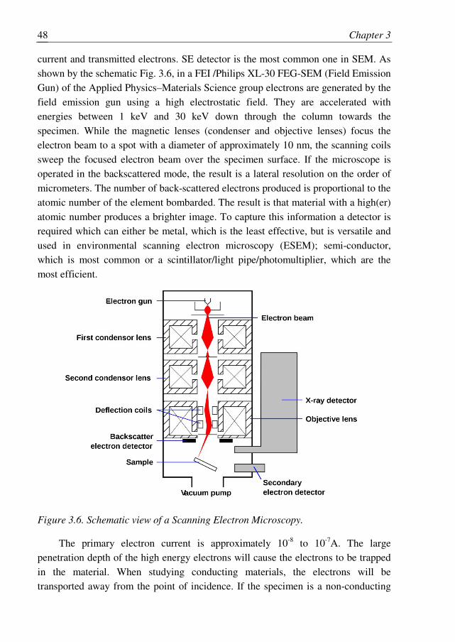
current and transmitted electrons. SE detector is the most common one in SEM. As
shown by the schematic Fig. 3.6, in a FEI /Philips XL-30 FEG-SEM (Field Emission
Gun) of the Applied Physics–Materials Science group electrons are generated by the
field emission gun using a high electrostatic field. They are accelerated with
energies between 1 keV and 30 keV down through the column towards the
specimen. While the magnetic lenses (condenser and objective lenses) focus the
electron beam to a spot with a diameter of approximately 10 nm, the scanning coils
sweep the focused electron beam over the specimen surface. If the microscope is
operated in the backscattered mode, the result is a lateral resolution on the order of
micrometers. The number of back-scattered electrons produced is proportional to the
atomic number of the element bombarded. The result is that material with a high(er)
atomic number produces a brighter image. To capture this information a detector is
required which can either be metal, which is the least effective, but is versatile and
used in environmental scanning electron microscopy (ESEM); semi-conductor,
which is most common or a scintillator/light pipe/photomultiplier, which are the
most efficient.
Figure 3.6. Schematic view of a Scanning Electron Microscopy.
The primary electron current is approximately 10-8 to 10-7A. The large
penetration depth of the high energy electrons will cause the electrons to be trapped
in the material. When studying conducting materials, the electrons will be
transported away from the point of incidence. If the specimen is a non-conducting
Characterization of nanoparticles
49
material, the excess electrons will cause charging of the surface. The electrostatic
charge on the surface deflects the incoming electrons, giving rise to distortion of the
image. To reduce surface charging effects, a conducting layer of metal, with typical
thicknesses 5-10 nm, can be sputtered onto the surface. This layer will transport the
excess electrons, reducing the negative charging effects. An adverse effect of the
sputtered layer is that it may diminish the resolving power of the microscope, since
topographical information is no longer gained from the surface of the material, but
from the sputtered layer. Charging of the surface is not the only factor determining
the resolution of a scanning electron microscope. The width of the electron beam is
also an important factor for the lateral resolution. A narrow electron beam results in
a high resolution. The spot size however, is a function of the accelerating voltage
2 22 2 2 6
20
1 1
2p c s
i Ed C C
B Eλ α α
α
∆ = + + + . (3.13)
The broadening of the spot size is the sum of broadening effects due to several
processes. The first contributor is the beam itself, B is the brightness of the source,
i is the beam current and α its divergence angle. The second part is the
contribution due to diffraction of the electrons of wavelength λ by the size of the
final aperture. The last two parts are the broadening caused by chromatic and
spherical aberrations. Where 0E is the electron energy and E∆ is the energy
spread, sC represents the spherical aberration and cC is the chromatic aberration
coefficient. To achieve the smallest spot size, all contributions should be as small as
possible. Decreasing the accelerating voltage will not only cause the wavelength of
the electrons to increase, but also the chromatic aberration increases as well,
resulting in increasing of the spot size and, as a consequence, a decrease in resolving
power of the microscope.
A field emission gun has a very high brightness B , reducing the contribution
in broadening due to the beam itself. The energy spread E∆ in the electron energies
is also small. Together with the fact that the coefficients sC and cC can be reduced
by optimizing the lenses for low-energy electrons, provides the FEG low voltage
scanning electron microscope with very high resolving power. In this thesis part of
the work is concentrated on silica particles. Since these particles are not electrical
conductive, the XL30-ESEM-FEG SEM in high vacuum and wet modes and FEI
Philips XL30s-FEG with TLD detector were used. All MK scanning electron
microscopes are equipped with field emission guns (FEG).
Chapter 3
50
3.4 Image processing and analysis
Digital image processing and analysis is the computer-aided manipulation with
an image aimed at improving the image quality and extracting useful information
about the objects depicted in the image [41]. Image processing is concerned with
transforming image, i.e. the input of the processing is an image; the output is an
image again. Image enhancement, restoration and segmentation are among the most
common image processing tasks. In image analysis we want to obtain quantitative
data from the images, such as dimensions of nanoparticles, their concentration and
fractal dimension; in this case, input consists of one or more images, whereas the
output contains numeric or symbolic data.
Images acquired by digital camera always contain noise and other artefacts
caused by imperfections in the measurement equipment: gain and offset of
individual elements of any multi-element detector will never be precisely the same.
These variations result from the physical nature of the scintillator and optical
coupling. Noise reduction is usually the first step in image processing methods. In
this thesis, all image processing and analysis methods are applied to TEM
micrographs. Advantage of TEM digital cameras is its ability to correct for gain
variations; they can be measured and cancelled automatically. Therefore this
processing was done during the image acquisition stage by digital camera software.
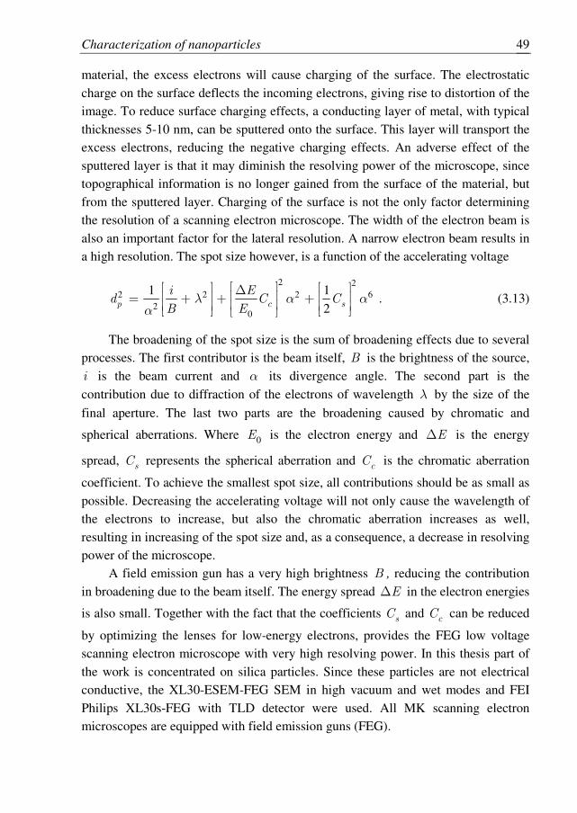
Figure 3.7 shows an example of a typical TEM image used in this study.
Figure 3.7. TEM image of agglomerates composed of multiple primary particles.
Characterization of nanoparticles
51
For image analysis to produce meaningful results, the spatial calibration must
be known. In our case, the magnification and other acquisition parameters can be
read from the microscope then the spatial calibration of the image can be
determined.
Further processing and analysis was performed with a Matlab software package
and the associated image processing toolbox. It is particularly well-suited for our
aim and enables one to concentrate on the image processing concepts and techniques
while keeping concerns about programming syntax and data management to a
minimum.
The first image processing step done in Matlab is thresholding. It is a basic
point transform which produces a binary image from a grey-scale image by setting
pixel values to 1 or 0 depending on whether they are above or below the threshold
value [42]. This is commonly used to separate or segment a region or object within
the image based upon its pixel values. In its basic operation, thresholding operates
on an image as follows
1
0
, ( , )( , )
,
if I x y thresholdI x y
otherwise
>= (3.14)
Thresholding is a primary operator for the separation of image foreground from
background. An important question is how to select an appropriate and efficient
threshold. Many image processing tasks require full automation, and there is often a
need for a criterion for selecting a threshold automatically. Selection of these criteria
is often based on actual consideration of image histogram. For a review and further
details references are made to [43-47]. However in our case, required precision of
threshold, low object contrast to the background and total number of images to
process, makes it more beneficial to inspect images by human eye and to set an
appropriate threshold manually.
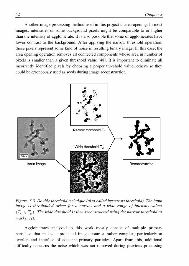
In this work we used a common variation of threshold – double threshold
method. The double threshold method consists in thresholding the input image for
two ranges of grey scale values, one being included in the other [48]. The threshold
for the narrow range is then used as a seed for the reconstruction of the threshold for
the wide range. The resulting binary image is much cleaner than that obtained with a
unique threshold. Moreover, the result is more stable to slight modifications of
threshold values. The double threshold technique is illustrated in Fig 3.8 for
extracting a shape of agglomerate that could not be obtained with a unique
threshold. Sometimes in the literature the double threshold technique is also called
hysteresis threshold [49].
Chapter 3
52
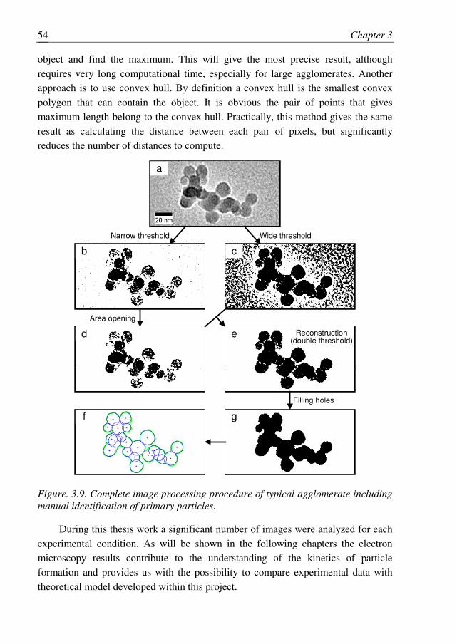
Another image processing method used in this project is area opening. In most
images, intensities of some background pixels might be comparable to or higher
than the intensity of agglomerate. It is also possible that some of agglomerates have
lower contrast to the background. After applying the narrow threshold operation,
those pixels represent some kind of noise in resulting binary image. In this case, the
area opening operation removes all connected components whose area in number of
pixels is smaller than a given threshold value [48]. It is important to eliminate all
incorrectly identified pixels by choosing a proper threshold value; otherwise they
could be erroneously used as seeds during image reconstruction.
Figure. 3.8. Double threshold technique (also called hysteresis threshold). The input
image is thresholded twice: for a narrow and a wide range of intensity values
( )n wT T∈ . The wide threshold is then reconstructed using the narrow threshold as
marker set.
Agglomerates analyzed in this work mostly consist of multiple primary
particles; that makes a projected image contrast rather complex, particularly at
overlap and interface of adjacent primary particles. Apart from this, additional
difficulty concerns the noise which was not removed during previous processing
Characterization of nanoparticles
53
steps. These are the reasons for appearance of holes in a binary image after applying
the double threshold operation. The holes are defined as a set of background
components which are not connected to the image border [48]. For proper projected
area calculation it is required to remove all the holes. This is done by a function
from Matlab image processing toolbox. It uses a morphological reconstruction by
erosion where mask image equals the input image and marker is an image of
constant value having the same border values as the input image.
On majority of examined images some agglomerates extended beyond the edge
of the image. Certainly, they may introduce some bias when performing statistics on
particle measurements. Therefore it is necessary to remove all such objects from
further analysis. Particles where the contrast was too low to accurately separate
particle from background were also removed from evaluation.
The complete image processing procedure is demonstrated in Fig. 3.9. The
original grey-scale image (Fig. 3.9a) was modified using the operations mentioned
earlier and following closely the techniques described in literature [48,50,51]. So, to
summarize, the image processing consists of:
- Narrow thresholding of the original image (Fig. 3.9b).
- Noise removal by area opening of the binary image (Fig. 3.9d).
- Wide thresholding of the original image (Fig. 3.9c).
- The wide threshold reconstruction using the narrow threshold as marker set
(Fig. 3.9e).
- Filling holes in the binary image (Fig. 3.9g).
- Removal of agglomerates connected to the image border and low contrast
particles.
Examination of obtained binary image (Fig. 3.9g) needs to be performed to
verify the correct identification of particle boundaries with manual adjustments
where necessary. Final image after processing is presented in Fig. 3.9f. Identified
border of agglomerate is shown in green. Blue circles with center marks are primary
particles. Their diameter and position with respect to the geometric center of the
agglomerate was manually measured for each object. Agglomerates with
unidentified primary particles were rejected from the analysis.
Further image analysis was done automatically by in-house made Matlab code.
It allows us to determine the projected area of agglomerate, its maximum projected
length L and width W in the direction perpendicular to L . These parameters were
calculated by measuring a set of properties for each connected component (object) in
the binary image. The projected area is simply the actual number of pixels in the
object. But maximum projected length can be measured in different ways. In
principle, it is possible to calculate the distance between each pair of pixels in the
Chapter 3
54
object and find the maximum. This will give the most precise result, although
requires very long computational time, especially for large agglomerates. Another
approach is to use convex hull. By definition a convex hull is the smallest convex
polygon that can contain the object. It is obvious the pair of points that gives
maximum length belong to the convex hull. Practically, this method gives the same
result as calculating the distance between each pair of pixels, but significantly
reduces the number of distances to compute.
a
b c
d e
f g
Narrow threshold Wide threshold
Area opening
Reconstruction(double threshold)
Filling holes
Figure. 3.9. Complete image processing procedure of typical agglomerate including
manual identification of primary particles.
During this thesis work a significant number of images were analyzed for each
experimental condition. As will be shown in the following chapters the electron
microscopy results contribute to the understanding of the kinetics of particle
formation and provides us with the possibility to compare experimental data with
theoretical model developed within this project.
Characterization of nanoparticles
55
3.5 References
1. Louis de Broglie, Recherches sur la théorie des quanta, Thesis, Paris, 1924, Ann. de Physique (10)3 (1925) 22.
2. Busch H., Physik. Z. 23 (1922) 438; Ann.Physik 81 (1926) 974. 3. Haider M., Uhlemann S., Schwan E., Rose H., Kabius B. and Urban K., Nature,
392 (1998) 768. 4. Kabius B., Haider M., Uhlemann S., Schwan E., Urban K. and Rose H., J. Electron
Microsc. 51 (2002) S51. 5. Mantl S., Zhao Q. T. and Kabius B., MRS Bulletin 24 (1999) 31. 6. Lentzen M., Jahnen B., Jia C. L., Thust A., Tillmann K. and Urban K., Ultramicroscopy,
92 (2002) 233. 7. Dellby N., Krivanek L., Nellist D., Batson E. and Lupini R., J. Electron Microsc. 50
(2001) 177. 8. van Benthem K., Lupini A. R., Oxley M. P., Findlay S. D., Allen L. J. and Pennycook
S. J., Ultramicroscopy, 106 (2006) 1062. 9. Houdellier F., Warot-Fonrose B., Hÿtch M. J., Snoeck E., Calmels L., Serin V. and
Schattschneider P., Microsc. Microanal. 13 (2007) 48. 10. Kirkland A., Chang L.-Y., Haigh S. and Hetherington C., Curr. Appl Phys. 8 (2008) 425. 11. Kabius B., Hartel P., Haider M., Müller H., Uhlemann S., Loebau U., Zach J. and
Rose H., J. Electron Microsc. 58 (2009) 147. 12. Berger A., Mayer J. and Kohl H., Ultramicroscopy, 55 (1994) 101. 13. Zuo J. M., Kim M., O’Keeffe M. and Spence J. C. H., Nature, 401 (1999) 49. 14. Erni R., Aberration-Corrected Imaging in Transmission Electron Microscopy. An
Introduction, Imperial College Press, London, 2010. 15. De Hosson J. Th. M., In-situ transmission electron microscopy on metals, in: Van
Tendeloo G., Van Dyck D. and Pennycook S. J. (eds.), Handbook of Nanoscopy, Weinheim, Wiley-VCH, 2012, p. 1097.
16. De Hosson J.Th.M. and Van Veen A., in: Nalwa H. S. (ed.), Encyclopedia of
Nanoscience and Nanotechnology, American Scientific Publishers, vol. VII, 2004, p. 297.
17. Groen B., Misfit dislocation patterns studied with high resolution TEM, Thesis, University of Groningen, 1999.
18. Carvalho P. A., Planar defects in ordered systems, Thesis, University of Groningen, 2001.
19. Soer W., Interactions between dislocations and grain boundaries, Thesis, University of Groningen, 2006.
20. Chen Z., Superplasticity of coarse grained aluminum alloys, Thesis, University of Groningen, 2010.
21. Mogck S., Transmission electron microscopy studies of interfaces in multi-component systems, Thesis, University of Groningen, 2004.
22. Venkatesan S., Structural domains in thin films of ferroelectrics and multi-ferroics, Thesis, University of Groningen, 2010.
23. Punzhin S., Performance of ordered and disordered nanoporous metals, Thesis, University of Groningen, 2013.
24. Buseck P., Cowley J. and Eyring L. High Resolution Transmission Electron Microscopy, Oxford University Press, 1992.
25. De Hosson J. Th. M., in: Handbook of Microscopy, Amelinckx S., van Dyck D., van Landuyt J., van Tenderloo G. (eds.), Weinheim, VCH-publisher, vol. 3, 1997, p. 5.
Chapter 3
56
26. Spence J. C. H., Experimental High-Resolution Electron Microscopy, 2nd edn., Oxford University Press, 1988.
27. Williams D. B. and Carter C. B. Transmission Electron Microscopy. A Textbook for
Materials Science, Plenum, 1996. 28. Zhong Lin Wang, Elastic and Inelastic scattering in electron diffraction and imaging,
Plenum Press New York, 1995. 29. Egerton R. F., Physical Principles of Electron Microscopy: An Introduction to TEM,
SEM and AEM, Springer, 2005. 30. Burgess R. E., Houston J. M. and Houston J., Phys. Rev. 90 (1953) 515. 31. Reiner L., Image formation in LVSEM, SPIE Optical Engineering Press, 1st edn., 1993. 32. Zernike F., Zeitschrift für technische Physik, 16 (1935) 454; Phys. Z. 36 (1935) 848. 33. O’Keefe M.A., Ultramicroscopy, 47 (1992) 282. 34. Scherzer O., J. Appl. Phys. 20 (1949) 20. 35. Haider M., Rose H., Uhlemann S., Schwan E., Kabius B. and Urban K., Ultramicroscopy
75 (1998) 53. 36. EDAX Phoenix software,TEM Quant Materials, Version 3.2, Mahwah, New Jersey,
EDAX Inc. 2000. 37. Gonzalez R. C. and Woods R. E., Digital image processing, 3rd edn., Prentice Hall, 2007. 38. Young I. T., Gerbrands J. J. and van Vliet L. J., Fundamentals of image processing, Delft
University of Technology, 2007. 39. Knoll M., Z. Techn. Phys., 16 (1935) 467. 40. von Ardenne M., Z. Phys., 109 (1938) 553. 41. Wilkinson M. H. F. and Schut F. (eds.) Digital Image Analysis of Microbes: Imaging,
Morphometry, Fluorometry and Motility Techniques and Applications, John Wiley & Sons, 1998.
42. Solomon C. and Breckon T., Fundamentals of Digital Image Processing: A Practical Approach with Examples in MATLAB, John Wiley & Sons, 2011
43. Michielsen K. F. L., De Raedt H. and De Hosson J. Th. M., Adv. Imag. Elect. Phys. 125 (2002) 119.
44. Russ J. C.,The Image Processing Handbook, Florida, CRC Press, 1995. 45. Castleman K. R., Digital Image Processing, New Jersey, Prentice Hall, 1996. 46. Gonzalez R. C. and Woods R.E., Digital Image Processing, Massachusetts, Addison-
Wesley, 1993. 47. Rosenfeld A., Kak A. C., Digital Picture Processing, New York, Academic Press, 1982. 48. Soille P., Morphological Image Analysis: Principles and Applications, New York,
Springer-Verlag, 2003. 49. Canny J., IEEE Trans. Pattern Analysis and Machine Intelligence, PAMI-8(6) (1986)
679. 50. Smirnov B. M., Dutka M., van Essen V. M., Gersen S., Visser P., Vainchtein D.,
De Hosson J. Th. M., Levinsky H. B. and Mokhov A. V., Europhys. Lett. 98 (2012) 66005.
51. Boldridge D., J. Aerosol Sci. 44 (2010) 1821.


![University of Groningen Processing and structure of ... · types (Fig. 2.1): bottom-up and top-down approaches [7]. The latter refers to crushing of large objects, resulting in small](https://img.pdfslide.us/doc/110x75/60618ea4525600319e3ccaba/university-of-groningen-processing-and-structure-of-types-fig-21-bottom-up.jpg)