Embed Size (px)
Citation preview
TUSB3210Universal Serial BusGeneral-Purpose Device Controller
Data Manual
August 2007 DIBU
SLLS466F
Contents
TUSB3210Universal Serial BusGeneral-Purpose Device ControllerSLLS466F–FEBRUARY 2001–REVISED AUGUST 2007
1 Introduction......................................................................................................................... 71.1 Features....................................................................................................................... 71.2 Description.................................................................................................................... 71.3 Ordering Information ........................................................................................................ 71.4 Device Information........................................................................................................... 81.5 Revision History ............................................................................................................ 11
2 Functional Description ........................................................................................................ 122.1 MCU Memory Map ......................................................................................................... 122.2 Miscellaneous Registers .................................................................................................. 13
2.2.1 TUSB3210 Boot Operation..................................................................................... 132.2.2 MCNFG: MCU Configuration Register........................................................................ 132.2.3 PUR_n: GPIO Pullup Register for Port n (n = 0 to 3)....................................................... 142.2.4 INTCFG: Interrupt Configuration .............................................................................. 142.2.5 WDCSR: Watchdog Timer, Control, and Status Register.................................................. 142.2.6 PCON: Power Control Register (at SFR 87h) ............................................................... 15
2.3 Buffers + I/O RAM Map.................................................................................................... 162.4 Endpoint Descriptor Block (EDB-1 to EDB-3) .......................................................................... 18
2.4.1 OEPCNF_n: Output Endpoint Configuration (n = 1 to 3)................................................... 192.4.2 OEPBBAX_n: Output Endpoint X-Buffer Base Address (n = 1 to 3) ..................................... 202.4.3 OEPBCTX_n: Output Endpoint X-Byte Count (n = 1 to 3) ................................................. 202.4.4 OEPBBAY_n: Output Endpoint Y-Buffer Base Address (n = 1 to 3) ..................................... 202.4.5 OEPBCTY_n: Output Endpoint Y-Byte Count (n = 1 to 3) ................................................. 212.4.6 OEPSIZXY_n: Output Endpoint X-/Y-Buffer Size (n = 1 to 3) ............................................. 212.4.7 IEPCNF_n: Input Endpoint Configuration (n = 1 to 3) ...................................................... 212.4.8 IEPBBAX_n: Input Endpoint X-Buffer Base Address (n = 1 to 3) ......................................... 222.4.9 IEPBCTX_n: Input Endpoint X-Byte Base Address (n = 1 to 3)........................................... 222.4.10 IEPBBAY_n: Input Endpoint Y-Buffer Base Address (n = 1 to 3) ......................................... 232.4.11 IEPBCTY_n: Input Endpoint Y-Byte Count (n = 1 to 3) .................................................... 232.4.12 IEPSIZXY_n: Input Endpoint X-/Y-Buffer Size (n = 1 to 3) ................................................ 23
2.5 Endpoint-0 Descriptor Registers ......................................................................................... 242.5.1 IEPCNFG_0: Input Endpoint-0 Configuration Register..................................................... 242.5.2 IEPBCNT_0: Input Endpoint-0 Byte-Count Register........................................................ 252.5.3 OEPCNFG_0: Output Endpoint-0 Configuration Register ................................................. 252.5.4 OEPBCNT_0: Output Endpoint-0 Byte-Count Register .................................................... 26
2.6 USB Registers .............................................................................................................. 262.6.1 FUNADR: Function Address Register ........................................................................ 262.6.2 USBSTA: USB Status Register................................................................................ 272.6.3 USBMSK: USB Interrupt Mask Register...................................................................... 282.6.4 USBCTL: USB Control Register ............................................................................... 282.6.5 VIDSTA: VID/PID Status Register............................................................................. 29
2.7 Function Reset and Power-Up Reset Interconnect .................................................................... 292.8 Pullup Resistor Connect/Disconnect..................................................................................... 302.9 8052 Interrupt and Status Registers ..................................................................................... 30
2.9.1 8052 Standard Interrupt Enable Register .................................................................... 312.9.2 Additional Interrupt Sources.................................................................................... 312.9.3 VECINT: Vector Interrupt Register ............................................................................ 322.9.4 Logical Interrupt Connection Diagram (INT0)................................................................ 332.9.5 P2[7:0], P3.3 Interrupt (INT1) .................................................................................. 33
2.10 I2C Registers ................................................................................................................ 342.10.1 I2CSTA: I2C Status and Control Register.................................................................... 342.10.2 I2CADR: I2C Address Register ................................................................................ 35
Contents2 Submit Documentation Feedback
TUSB3210Universal Serial Bus
General-Purpose Device ControllerSLLS466F–FEBRUARY 2001–REVISED AUGUST 2007
2.10.3 I2CDAI: I2C Data-Input Register .............................................................................. 352.10.4 I2CDAO: I2C Data-Output Register ........................................................................... 35
2.11 Read/Write Operations .................................................................................................... 352.11.1 Read Operation (Serial EEPROM) ............................................................................ 352.11.2 Current Address Read Operation ............................................................................. 362.11.3 Sequential Read Operation .................................................................................... 362.11.4 Write Operation (Serial EEPROM) ............................................................................ 372.11.5 Page Write Operation ........................................................................................... 37
3 Specifications .................................................................................................................... 393.1 Absolute Maximum Ratings............................................................................................... 393.2 Commercial Operating Conditions ....................................................................................... 393.3 Electrical Characteristics .................................................................................................. 39
4 Application ........................................................................................................................ 404.1 Examples .................................................................................................................... 404.2 Reset Timing................................................................................................................ 41
Contents 3
TUSB3210Universal Serial BusGeneral-Purpose Device ControllerSLLS466F–FEBRUARY 2001–REVISED AUGUST 2007
List of Figures1-1 TUSB3210 Block Diagram ........................................................................................................ 8
1-2 Terminal Assignments ............................................................................................................. 9
2-1 MCU Memory Map (TUSB3210) ................................................................................................ 12
2-2 Reset Diagram..................................................................................................................... 30
2-3 Pullup Resistor Connect/Disconnect Circuit ................................................................................... 30
2-4 Internal Vector Interrupt (INT0).................................................................................................. 33
2-5 P2[7:0], P3.3 Input Port Interrupt Generation ................................................................................. 33
4-1 Example LED Connection........................................................................................................ 40
4-2 Partial Connection Bus Power Mode ........................................................................................... 40
4-3 Upstream Connection (a) Non-Switching Power Mode (b) Switching Power Mode...................................... 41
4-4 Reset Timing....................................................................................................................... 42
List of Figures4 Submit Documentation Feedback
TUSB3210Universal Serial Bus
General-Purpose Device ControllerSLLS466F–FEBRUARY 2001–REVISED AUGUST 2007
List of Tables1-1 Terminal Functions ................................................................................................................. 9
1-2 Test0/Test1 Functions ............................................................................................................ 10
2-1 XDATA Space ..................................................................................................................... 16
2-2 Memory-Mapped Register Summary (XDATA Range = FF80 → FFFF) .................................................. 17
2-3 EDB and Buffer Allocations in XDATA ......................................................................................... 18
2-4 EDB Entries in RAM (n = 1 to 3) ................................................................................................ 19
2-5 Input/Output EDB-0 Registers................................................................................................... 24
2-6 External Pin Mapping to S[3:0] in VIDSTA Register.......................................................................... 29
2-7 8052 Interrupt Location Map..................................................................................................... 30
2-8 Vector Interrupt Values ........................................................................................................... 32
List of Tables 5
TUSB3210Universal Serial BusGeneral-Purpose Device ControllerSLLS466F–FEBRUARY 2001–REVISED AUGUST 2007
List of Tables6 Submit Documentation Feedback
www.ti.com
1 Introduction
1.1 Features
1.2 Description
1.3 Ordering Information
TUSB3210Universal Serial Bus
General-Purpose Device ControllerSLLS466F–FEBRUARY 2001–REVISED AUGUST 2007
– 512 × 8 Shared RAM Used for Data Buffers and• Multiproduct Support With One Code and OneEndpoint Descriptor Blocks (EDB) (2)Chip (up to 16 Products With One Chip)
– Four 8052 GPIO Ports, Ports 0,1, 2, and 3• Fully Compliant With USB 2.0 Full-Speed– Master I2C Controller for External SlaveSpecifications: TID #40270269
Device Access• Supports 12 Mbits/s USB Data Rate (Full– Watchdog TimerSpeed)• Operates From a 12-MHz Crystal• Supports USB Suspend/Resume and
Remote Wake-up Operation • On-Chip PLL Generates 48 MHz• Integrated 8052 Microcontroller With: • Supports a Total of 3 Input and 3 Output
(Interrupt, Bulk) Endpoints– 256 × 8 RAM for Internal Data– 8K × 8 RAM Code Space Available for • Powerdown Mode
Downloadable Firmware From Host or I2C • 64-Pin TQFP PackagePort. (1)
• Applications Include Keyboard, Bar CodeReader, Flash Memory Reader, General-Purpose Controller
(1) The TUSB3210 has 8K × 8 RAM for development. (2) This is the buffer space for USB packet transactions.
The TUSB3210 is a USB-based controller targeted as a general-purpose MCU with GPIO. The TUSB3210has 8K × 8 RAM space for application development. In addition, the programmability of the TUSB3210makes it flexible enough to use for various other general USB I/O applications. Unique vendoridentification and product identification (VID/PID) can be selected without the use of an external EEPROM.Using a 12-MHz crystal, the onboard oscillator generates the internal system clocks. The device can beprogrammed via an inter-IC (I2C) serial interface at power on from an EEPROM, or optionally, theapplication firmware can be downloaded from a host PC via USB. The popular 8052-basedmicroprocessor allows several third-party standard tools to be used for application development. Inaddition, the vast amounts of application code available in the general market also can be used (this mayor may not require some code modification due to hardware variations).
OPERATINGPACKAGE PACKAGE ORDERING TRANSPORTPRODUCT PACKAGE (1) (2) TEMPERATURECODE MARKING NUMBER MEDIARANGE
Plastic quadTUSB3210PM PM 0°C to 70°C TUSB3210PM TUSB3210PM 160-piece trayflatpack 64
(1) Package drawings, standard packing quantities, thermal data, symbolization, and PCB design guidelines are available atwww.ti.com/sc/package.
(2) For the most current package and ordering information, see the Package Option Addendum at the end of this document, or see the TIwebsite at www.ti.com.
Please be aware that an important notice concerning availability, standard warranty, and use in critical applications of TexasInstruments semiconductor products and disclaimers thereto appears at the end of this document.
PRODUCTION DATA information is current as of publication date. Copyright © 2001–2007, Texas Instruments IncorporatedProducts conform to specifications per the terms of the TexasInstruments standard warranty. Production processing does notnecessarily include testing of all parameters.
www.ti.com
1.4 Device Information
RSTI8052Core
86K × 8ROM
8K × 8RAM
512 × 8SRAM
CPU − I/FSuspend/Resume
UBMUSB Buffer
Manager
TDMControlLogic
USBSIE
USBTxR
8
8
8
88
USB-0
PLLand
Dividers
ClockOscillator
12 MHz
82 × 16-Bit
Timers
I2CController
8
8
Reset,Interruptand WDT
8 P0.[7:0]
8 P1.[7:0]
8 P2.[7:0]
8 P3.[7:0]
I2C Bus
Port 0
Port 1
Port 2
Port 3
Logic
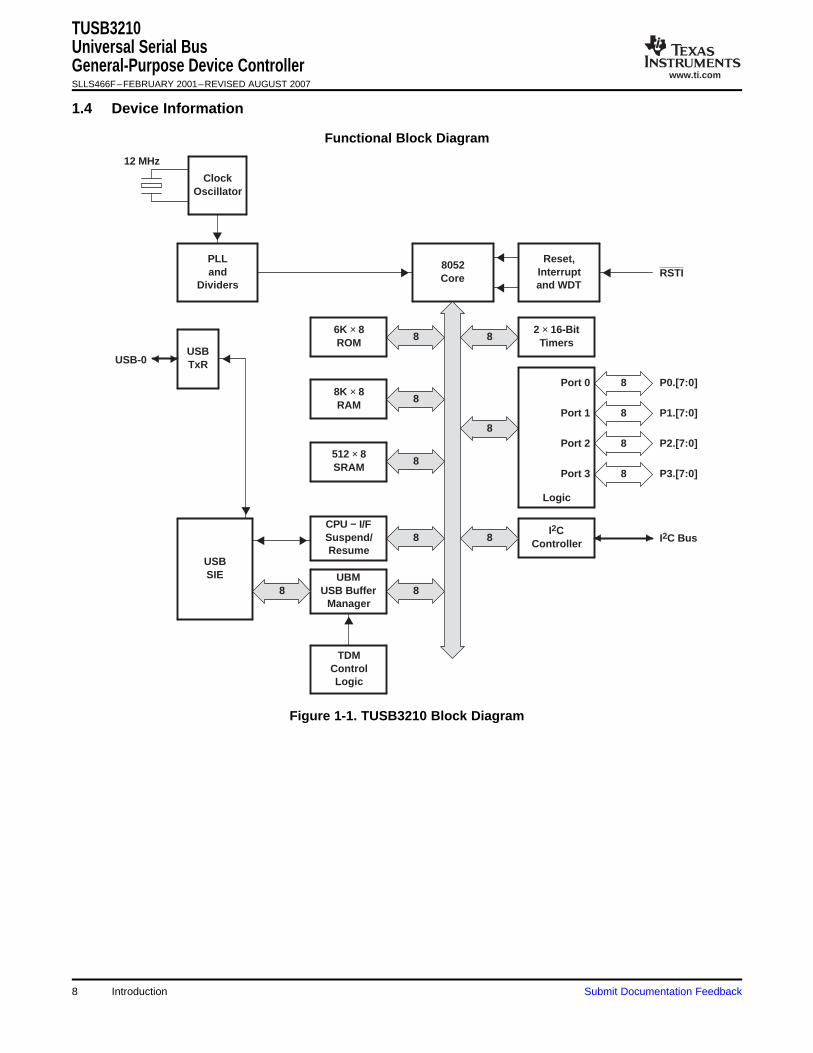
TUSB3210Universal Serial BusGeneral-Purpose Device ControllerSLLS466F–FEBRUARY 2001–REVISED AUGUST 2007
Functional Block Diagram
Figure 1-1. TUSB3210 Block Diagram
Introduction8 Submit Documentation Feedback
www.ti.com
1 2 3
P1.1P1.0P2.7P2.6P2.5P2.4P2.3P2.2GNDP2.1P2.0GNDTEST2DMDPPUR
32
31
30
29
28
27
26
25
24
23
22
21
20
19
18
174
49
50
51
52
53
54
55
56
57
58
59
60
61
62
63
64
P0.6P0.7P3.7P3.6P3.5P3.4P3.3P3.2
P3.1/S1/TXDP3.0/S0/RXD
GNDX2X1
VCCNCNC
5 6 7 8
P1.
3
VR
EN
47 46 45 44 4348 42
P0.
3P
0.2
P0.
1P
0.0
GN
DP
1.7
P1.
6V
CC
SD
AS
CL
RS
T
NC
GN
DR
SV
NC
NC S2
S3
40 39 3841
9 10 11 12 13
37 36
RS
V
1.8V
DD
P1.
5
35 34 33
14 15 16
TE
ST
0T
ES
T1
SU
SP
P1.
4
VC
C
P1.
2
P0.
5P
0.4
NC
PM PACKAGE(TOP VIEW)
TUSB3210Universal Serial Bus
General-Purpose Device ControllerSLLS466F–FEBRUARY 2001–REVISED AUGUST 2007
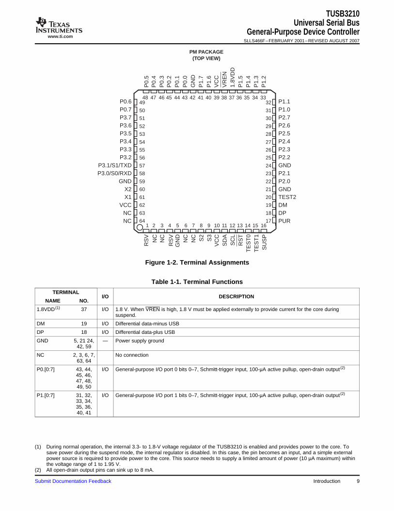
Figure 1-2. Terminal Assignments
Table 1-1. Terminal Functions
TERMINALI/O DESCRIPTION
NAME NO.
1.8VDD (1) 37 I/O 1.8 V. When VREN is high, 1.8 V must be applied externally to provide current for the core duringsuspend.
DM 19 I/O Differential data-minus USB
DP 18 I/O Differential data-plus USB
GND 5, 21 24, — Power supply ground42, 59
NC 2, 3, 6, 7, No connection63, 64
P0.[0:7] 43, 44, I/O General-purpose I/O port 0 bits 0–7, Schmitt-trigger input, 100-μA active pullup, open-drain output (2)
45, 46,47, 48,49, 50
P1.[0:7] 31, 32, I/O General-purpose I/O port 1 bits 0–7, Schmitt-trigger input, 100-μA active pullup, open-drain output (2)
33, 34,35, 36,40, 41
(1) During normal operation, the internal 3.3- to 1.8-V voltage regulator of the TUSB3210 is enabled and provides power to the core. Tosave power during the suspend mode, the internal regulator is disabled. In this case, the pin becomes an input, and a simple externalpower source is required to provide power to the core. This source needs to supply a limited amount of power (10 μA maximum) withinthe voltage range of 1 to 1.95 V.
(2) All open-drain output pins can sink up to 8 mA.
Submit Documentation Feedback Introduction 9
www.ti.com
TUSB3210Universal Serial BusGeneral-Purpose Device ControllerSLLS466F–FEBRUARY 2001–REVISED AUGUST 2007
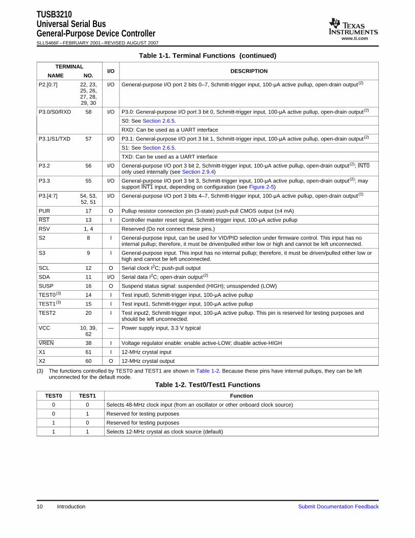
Table 1-1. Terminal Functions (continued)
TERMINALI/O DESCRIPTION
NAME NO.
P2.[0:7] 22, 23, I/O General-purpose I/O port 2 bits 0–7, Schmitt-trigger input, 100-μA active pullup, open-drain output (2)
25, 26,27, 28,29, 30
P3.0/S0/RXD 58 I/O P3.0: General-purpose I/O port 3 bit 0, Schmitt-trigger input, 100-μA active pullup, open-drain output (2)
S0: See Section 2.6.5.
RXD: Can be used as a UART interface
P3.1/S1/TXD 57 I/O P3.1: General-purpose I/O port 3 bit 1, Schmitt-trigger input, 100-μA active pullup, open-drain output (2)
S1: See Section 2.6.5.
TXD: Can be used as a UART interface
P3.2 56 I/O General-purpose I/O port 3 bit 2, Schmitt-trigger input, 100-μA active pullup, open-drain output (2); INT0only used internally (see Section 2.9.4)
P3.3 55 I/O General-purpose I/O port 3 bit 3, Schmitt-trigger input, 100-μA active pullup, open-drain output (2); maysupport INT1 input, depending on configuration (see Figure 2-5)
P3.[4:7] 54, 53, I/O General-purpose I/O port 3 bits 4–7, Schmitt-trigger input, 100-μA active pullup, open-drain output (2)
52, 51
PUR 17 O Pullup resistor connection pin (3-state) push-pull CMOS output (±4 mA)
RST 13 I Controller master reset signal, Schmitt-trigger input, 100-μA active pullup
RSV 1, 4 Reserved (Do not connect these pins.)
S2 8 I General-purpose input, can be used for VID/PID selection under firmware control. This input has nointernal pullup; therefore, it must be driven/pulled either low or high and cannot be left unconnected.
S3 9 I General-purpose input. This input has no internal pullup; therefore, it must be driven/pulled either low orhigh and cannot be left unconnected.
SCL 12 O Serial clock I2C; push-pull output
SDA 11 I/O Serial data I2C; open-drain output(2)
SUSP 16 O Suspend status signal: suspended (HIGH); unsuspended (LOW)
TEST0 (3) 14 I Test input0, Schmitt-trigger input, 100-μA active pullup
TEST1 (3) 15 I Test input1, Schmitt-trigger input, 100-μA active pullup
TEST2 20 I Test input2, Schmitt-trigger input, 100-μA active pullup. This pin is reserved for testing purposes andshould be left unconnected.
VCC 10, 39, — Power supply input, 3.3 V typical62
VREN 38 I Voltage regulator enable: enable active-LOW; disable active-HIGH
X1 61 I 12-MHz crystal input
X2 60 O 12-MHz crystal output
(3) The functions controlled by TEST0 and TEST1 are shown in Table 1-2. Because these pins have internal pullups, they can be leftunconnected for the default mode.
Table 1-2. Test0/Test1 Functions
TEST0 TEST1 Function
0 0 Selects 48-MHz clock input (from an oscillator or other onboard clock source)
0 1 Reserved for testing purposes
1 0 Reserved for testing purposes
1 1 Selects 12-MHz crystal as clock source (default)
Introduction10 Submit Documentation Feedback
www.ti.com
1.5 Revision History
TUSB3210Universal Serial Bus
General-Purpose Device ControllerSLLS466F–FEBRUARY 2001–REVISED AUGUST 2007
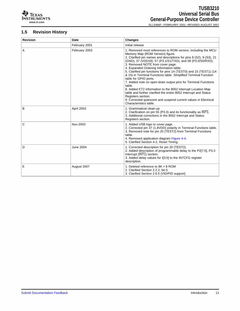
Revision Date Changes
February 2001 Initial release
A February 2003 1. Removed most references to ROM version, including the MCUMemory Map (ROM Version) figure.2. Clarified pin names and descriptions for pins 8 (S2), 9 (S3), 21(GND), 37 (VDD18), 57 (P3.1/S1/TXD), and 58 (P3.0/S0/RXD).3. Removed NOTE from cover page.4. Expanded Ordering Information table.5. Clarified pin functions for pins 14 (TEST0) and 15 (TEST1) (14& 15) in Terminal Functions table. Simplified Terminal Functiontable for GPIO ports.7. Added note on open-drain output pins for Terminal Functionstable.8. Added ET2 information to the 8052 Interrupt Location Maptable and further clarified the entire 8052 Interrupt and StatusRegisters section.9. Corrected quiescent and suspend current values in ElectricalCharacteristics table.
B April 2003 1. Grammatical clean-up2. Clarification on pin 55 (P3.3) and its functionality as INT1.3. Additional corrections in the 8052 Interrupt and StatusRegisters section.
C Nov-2003 1. Added USB logo to cover page.2. Corrected pin 37 (1.8VDD) polarity in Terminal Functions table.3. Removed note for pin 20 (TEST2) from Terminal Functionstable.4. Removed application diagram Figure 4-4.5. Clarified Section 4-2, Reset Timing
D June 2004 1. Corrected description for pin 20 (TEST2).2. Added description of programmable delay to the P2[7:0], P3.3Interrupt (INT1) section.3. Added delay values for I[3:0] to the INTCFG registerdescription.
E August 2007 1. Deleted reference to 8K × 8 ROM2. Clarified Section 2.2.2, bit 0.3. Clarified Section 2.6.5 (VID/PID support)
Submit Documentation Feedback Introduction 11
www.ti.com
2 Functional Description
2.1 MCU Memory Map
0000
Boot Mode (SDW = 0)
CODE
6K Boot ROM
17FF
1FFF
6K Boot ROM
97FF
8000
FD80
FFFF
FF80
8KRAM
Read/Write
XDATA
MMR
512 BytesRAM
8KCode RAMRead Only
CODE
Normal Mode (SDW = 1)
6K Boot ROM
XDATA
MMR
512 BytesRAM
TUSB3210Universal Serial BusGeneral-Purpose Device ControllerSLLS466F–FEBRUARY 2001–REVISED AUGUST 2007
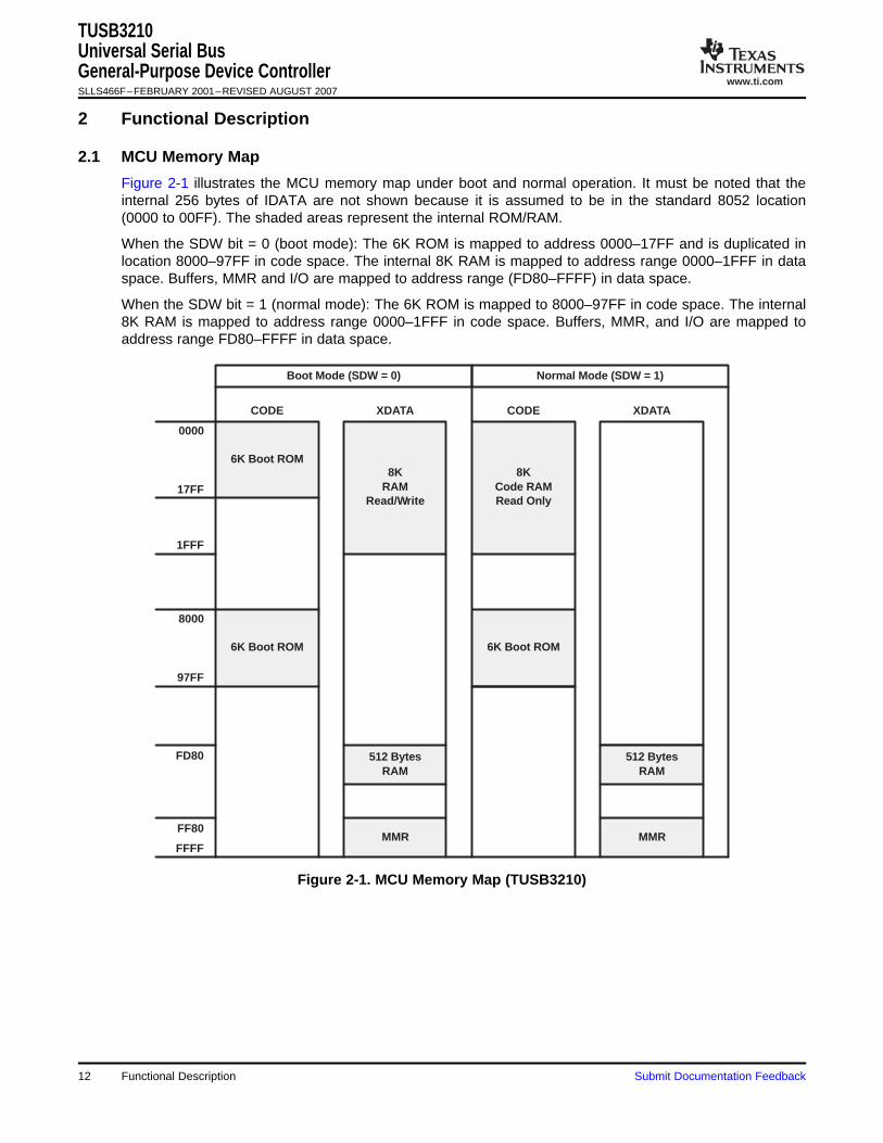
Figure 2-1 illustrates the MCU memory map under boot and normal operation. It must be noted that theinternal 256 bytes of IDATA are not shown because it is assumed to be in the standard 8052 location(0000 to 00FF). The shaded areas represent the internal ROM/RAM.
When the SDW bit = 0 (boot mode): The 6K ROM is mapped to address 0000–17FF and is duplicated inlocation 8000–97FF in code space. The internal 8K RAM is mapped to address range 0000–1FFF in dataspace. Buffers, MMR and I/O are mapped to address range (FD80–FFFF) in data space.
When the SDW bit = 1 (normal mode): The 6K ROM is mapped to 8000–97FF in code space. The internal8K RAM is mapped to address range 0000–1FFF in code space. Buffers, MMR, and I/O are mapped toaddress range FD80–FFFF in data space.
Figure 2-1. MCU Memory Map (TUSB3210)
12 Functional Description Submit Documentation Feedback
www.ti.com
2.2 Miscellaneous Registers
2.2.1 TUSB3210 Boot Operation
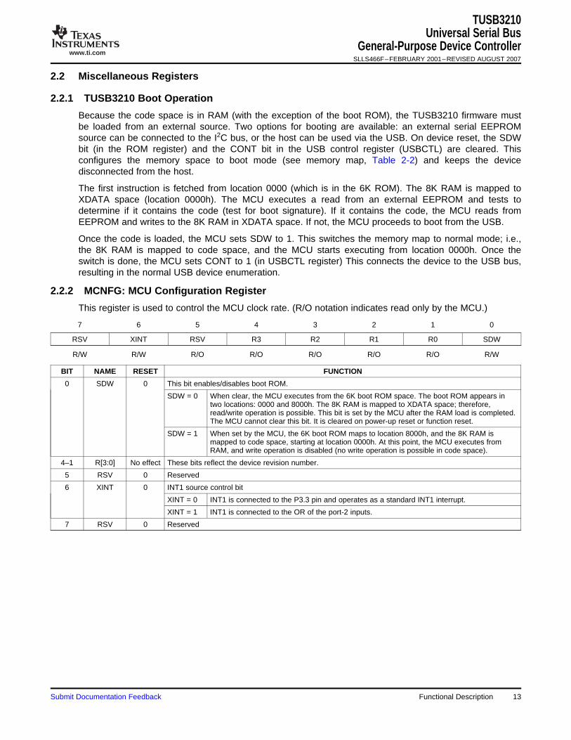
2.2.2 MCNFG: MCU Configuration Register
TUSB3210Universal Serial Bus
General-Purpose Device ControllerSLLS466F–FEBRUARY 2001–REVISED AUGUST 2007
Because the code space is in RAM (with the exception of the boot ROM), the TUSB3210 firmware mustbe loaded from an external source. Two options for booting are available: an external serial EEPROMsource can be connected to the I2C bus, or the host can be used via the USB. On device reset, the SDWbit (in the ROM register) and the CONT bit in the USB control register (USBCTL) are cleared. Thisconfigures the memory space to boot mode (see memory map, Table 2-2) and keeps the devicedisconnected from the host.
The first instruction is fetched from location 0000 (which is in the 6K ROM). The 8K RAM is mapped toXDATA space (location 0000h). The MCU executes a read from an external EEPROM and tests todetermine if it contains the code (test for boot signature). If it contains the code, the MCU reads fromEEPROM and writes to the 8K RAM in XDATA space. If not, the MCU proceeds to boot from the USB.
Once the code is loaded, the MCU sets SDW to 1. This switches the memory map to normal mode; i.e.,the 8K RAM is mapped to code space, and the MCU starts executing from location 0000h. Once theswitch is done, the MCU sets CONT to 1 (in USBCTL register) This connects the device to the USB bus,resulting in the normal USB device enumeration.
This register is used to control the MCU clock rate. (R/O notation indicates read only by the MCU.)
7 6 5 4 3 2 1 0
RSV XINT RSV R3 R2 R1 R0 SDW
R/W R/W R/O R/O R/O R/O R/O R/W
BIT NAME RESET FUNCTION
0 SDW 0 This bit enables/disables boot ROM.
SDW = 0 When clear, the MCU executes from the 6K boot ROM space. The boot ROM appears intwo locations: 0000 and 8000h. The 8K RAM is mapped to XDATA space; therefore,read/write operation is possible. This bit is set by the MCU after the RAM load is completed.The MCU cannot clear this bit. It is cleared on power-up reset or function reset.
SDW = 1 When set by the MCU, the 6K boot ROM maps to location 8000h, and the 8K RAM ismapped to code space, starting at location 0000h. At this point, the MCU executes fromRAM, and write operation is disabled (no write operation is possible in code space).
4–1 R[3:0] No effect These bits reflect the device revision number.
5 RSV 0 Reserved
6 XINT 0 INT1 source control bit
XINT = 0 INT1 is connected to the P3.3 pin and operates as a standard INT1 interrupt.
XINT = 1 INT1 is connected to the OR of the port-2 inputs.
7 RSV 0 Reserved
Submit Documentation Feedback Functional Description 13
www.ti.com
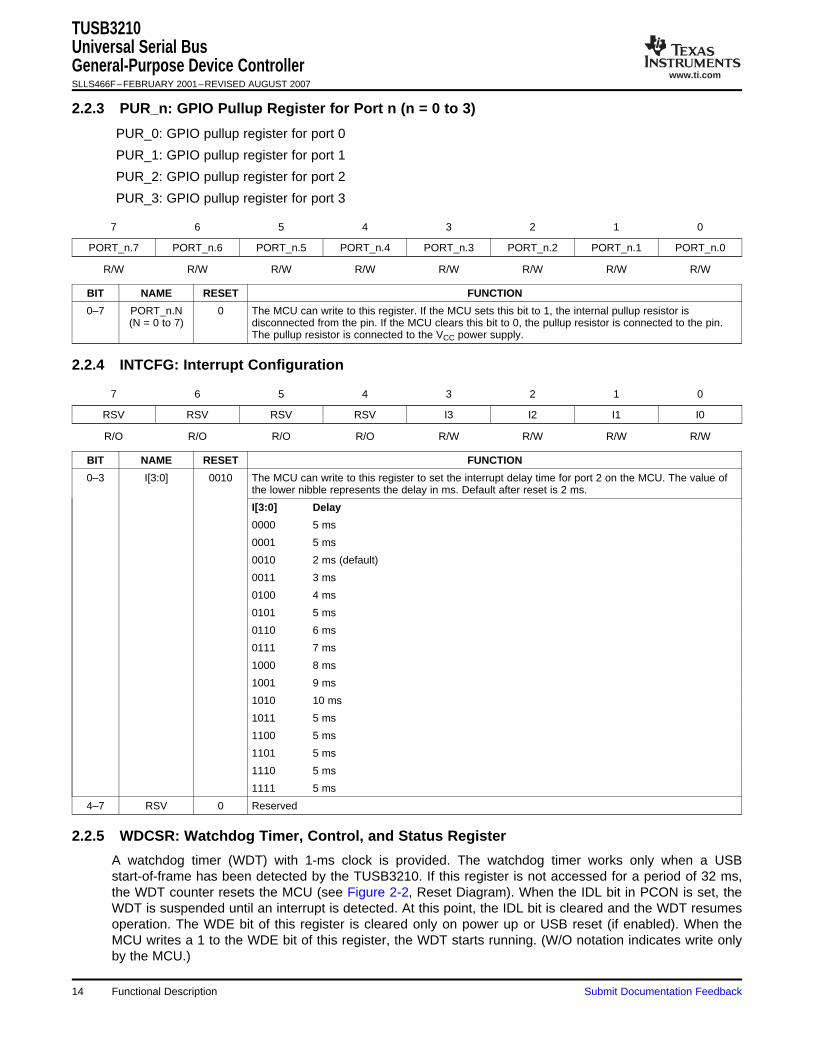
2.2.3 PUR_n: GPIO Pullup Register for Port n (n = 0 to 3)
2.2.4 INTCFG: Interrupt Configuration
2.2.5 WDCSR: Watchdog Timer, Control, and Status Register
TUSB3210Universal Serial BusGeneral-Purpose Device ControllerSLLS466F–FEBRUARY 2001–REVISED AUGUST 2007
PUR_0: GPIO pullup register for port 0
PUR_1: GPIO pullup register for port 1
PUR_2: GPIO pullup register for port 2
PUR_3: GPIO pullup register for port 3
7 6 5 4 3 2 1 0
PORT_n.7 PORT_n.6 PORT_n.5 PORT_n.4 PORT_n.3 PORT_n.2 PORT_n.1 PORT_n.0
R/W R/W R/W R/W R/W R/W R/W R/W
BIT NAME RESET FUNCTION
0–7 PORT_n.N 0 The MCU can write to this register. If the MCU sets this bit to 1, the internal pullup resistor is(N = 0 to 7) disconnected from the pin. If the MCU clears this bit to 0, the pullup resistor is connected to the pin.
The pullup resistor is connected to the VCC power supply.
7 6 5 4 3 2 1 0
RSV RSV RSV RSV I3 I2 I1 I0
R/O R/O R/O R/O R/W R/W R/W R/W
BIT NAME RESET FUNCTION
0–3 I[3:0] 0010 The MCU can write to this register to set the interrupt delay time for port 2 on the MCU. The value ofthe lower nibble represents the delay in ms. Default after reset is 2 ms.
I[3:0] Delay
0000 5 ms
0001 5 ms
0010 2 ms (default)
0011 3 ms
0100 4 ms
0101 5 ms
0110 6 ms
0111 7 ms
1000 8 ms
1001 9 ms
1010 10 ms
1011 5 ms
1100 5 ms
1101 5 ms
1110 5 ms
1111 5 ms
4–7 RSV 0 Reserved
A watchdog timer (WDT) with 1-ms clock is provided. The watchdog timer works only when a USBstart-of-frame has been detected by the TUSB3210. If this register is not accessed for a period of 32 ms,the WDT counter resets the MCU (see Figure 2-2, Reset Diagram). When the IDL bit in PCON is set, theWDT is suspended until an interrupt is detected. At this point, the IDL bit is cleared and the WDT resumesoperation. The WDE bit of this register is cleared only on power up or USB reset (if enabled). When theMCU writes a 1 to the WDE bit of this register, the WDT starts running. (W/O notation indicates write onlyby the MCU.)
Functional Description14 Submit Documentation Feedback
www.ti.com
2.2.6 PCON: Power Control Register (at SFR 87h)
TUSB3210Universal Serial Bus
General-Purpose Device ControllerSLLS466F–FEBRUARY 2001–REVISED AUGUST 2007
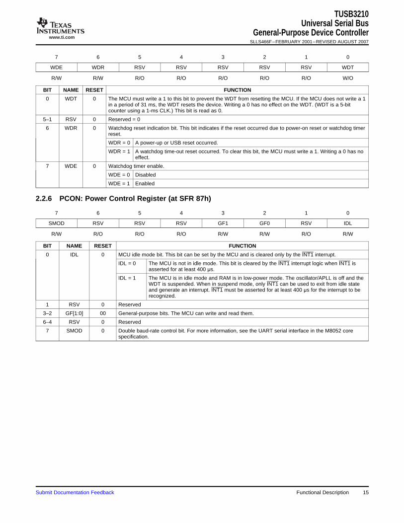
7 6 5 4 3 2 1 0
WDE WDR RSV RSV RSV RSV RSV WDT
R/W R/W R/O R/O R/O R/O R/O W/O
BIT NAME RESET FUNCTION
0 WDT 0 The MCU must write a 1 to this bit to prevent the WDT from resetting the MCU. If the MCU does not write a 1in a period of 31 ms, the WDT resets the device. Writing a 0 has no effect on the WDT. (WDT is a 5-bitcounter using a 1-ms CLK.) This bit is read as 0.
5–1 RSV 0 Reserved = 0
6 WDR 0 Watchdog reset indication bit. This bit indicates if the reset occurred due to power-on reset or watchdog timerreset.
WDR = 0 A power-up or USB reset occurred.
WDR = 1 A watchdog time-out reset occurred. To clear this bit, the MCU must write a 1. Writing a 0 has noeffect.
7 WDE 0 Watchdog timer enable.
WDE = 0 Disabled
WDE = 1 Enabled
7 6 5 4 3 2 1 0
SMOD RSV RSV RSV GF1 GF0 RSV IDL
R/W R/O R/O R/O R/W R/W R/O R/W
BIT NAME RESET FUNCTION
0 IDL 0 MCU idle mode bit. This bit can be set by the MCU and is cleared only by the INT1 interrupt.
IDL = 0 The MCU is not in idle mode. This bit is cleared by the INT1 interrupt logic when INT1 isasserted for at least 400 μs.
IDL = 1 The MCU is in idle mode and RAM is in low-power mode. The oscillator/APLL is off and theWDT is suspended. When in suspend mode, only INT1 can be used to exit from idle stateand generate an interrupt. INT1 must be asserted for at least 400 μs for the interrupt to berecognized.
1 RSV 0 Reserved
3–2 GF[1:0] 00 General-purpose bits. The MCU can write and read them.
6–4 RSV 0 Reserved
7 SMOD 0 Double baud-rate control bit. For more information, see the UART serial interface in the M8052 corespecification.
Submit Documentation Feedback Functional Description 15
www.ti.com
2.3 Buffers + I/O RAM Map
TUSB3210Universal Serial BusGeneral-Purpose Device ControllerSLLS466F–FEBRUARY 2001–REVISED AUGUST 2007
The address range from FD80 to FFFF is reserved for data buffers, setup packet, endpoint descriptorblocks (EDB), and all I/O. RAM space of 512 bytes [FD80–FF7F] is used for EDB and buffers. TheFF80–FFFF range is used for memory-mapped registers (MMR). Table 2-1 represents the internal XDATAspace allocation.
Table 2-1. XDATA Space
DESCRIPTION ADDRESS RANGE
FFFF
Internalmemory-mapped registers ↑
(MMR)
FF80
FF7F
Endpoint descriptor blocks ↑(EDB)
FF08
FF07
Setup packet buffer ↑
FF00
FEFF512-ByteInput endpoint-0 buffer ↑ RAM
FEF8
FEF7
Output endpoint-0 buffer ↑
FEF0
FEEF
Data buffers ↑(368 bytes)
FD80
Functional Description16 Submit Documentation Feedback
www.ti.com
TUSB3210Universal Serial Bus
General-Purpose Device ControllerSLLS466F–FEBRUARY 2001–REVISED AUGUST 2007
Table 2-2. Memory-Mapped Register Summary (XDATA Range = FF80 → FFFF)
ADDRESS REGISTER DESCRIPTION
FFFF FUNADR FUNADR: Function address register
FFFE USBSTA USBSTA: USB status register
FFFD USBMSK USBMSK: USB interrupt mask register
FFFC USBCTL USBCTL: USB control register
↑ RESERVED
FFF6 VIDSTA VIDSTA: VID/PID status register
↑ RESERVED
FFF3 I2CADR I2CADR: I2C address register
FFF2 I2CDAI I2CDAI: I2C data-input register
FFF1 I2CDAO I2CDAO: I2C data-output register
FFF0 I2CSTA I2CSTA: I2C status and control register
↑ RESERVED
FF97 PUR3 Port 3 pullup resistor register
FF96 PUR2 Port 2 pullup resistor register
FF95 PUR1 Port 1 pullup resistor register
FF94 PUR0 Port 0 pullup resistor register
FF93 WDCSR WDCSR: Watchdog timer, control and status register
FF92 VECINT VECINT: Vector interrupt register
FF91 RESERVED
FF90 MCNFG MCNFG: MCU configuration register
↑ RESERVED
FF84 INTCFG INTCFG: Interrupt delay configuration register
FF83 OEPBCNT_0 OEPBCNT_0: Output endpoint-0 byte count register
FF82 OEPCNFG_0 OEPCNFG_0: Output endpoint-0 configuration register
FF81 IEPBCNT_0 IEPBCNT_0: Input endpoint-0 byte count register
FF80 IEPCNFG_0 IEPCNFG_0: Input endpoint-0 configuration register
Submit Documentation Feedback Functional Description 17
www.ti.com
2.4 Endpoint Descriptor Block (EDB-1 to EDB-3)
TUSB3210Universal Serial BusGeneral-Purpose Device ControllerSLLS466F–FEBRUARY 2001–REVISED AUGUST 2007
Data transfers between USB, MCU and external devices are defined by an endpoint descriptor block(EDB). Four input and four output EDBs are provided. With the exception of EDB-0 (I/O endpoint 0), allEDBs are located in SRAM as shown in Table 2-3. Each EDB contains information describing the X and Ybuffers. In addition, it provides general status information.
Table 2-3. EDB and Buffer Allocations in XDATA
ADDRESS SIZE DESCRIPTION
FF7F
↑ 32 bytes RESERVED
FF60
FF5F
↑ 8 bytes Input endpoint 3: configuration
FF58
FF57
↑ 8 bytes Input endpoint 2: configuration
FF50
FF4F
↑ 8 bytes Input endpoint 1: configuration
FF48
FF47
↑ 40 bytes RESERVED
FF20
FF1F
↑ 8 bytes Output endpoint 3: configuration
FF18
FF17
↑ 8 bytes Output endpoint 2: configuration
FF10
FF0F
↑ 8 bytes Output endpoint 1: configuration
FF08
FF07
↑ 8 bytes Setup packet block
FF00
FEFF
↑ 8 bytes Input endpoint 0: buffer
FEF8
FEF7
↑ 8 bytes Output endpoint 0: buffer
FEF0
FEEF Top of buffer space
↑ 368 bytes Buffer space
FD80 Start of buffer space
Functional Description18 Submit Documentation Feedback
www.ti.com
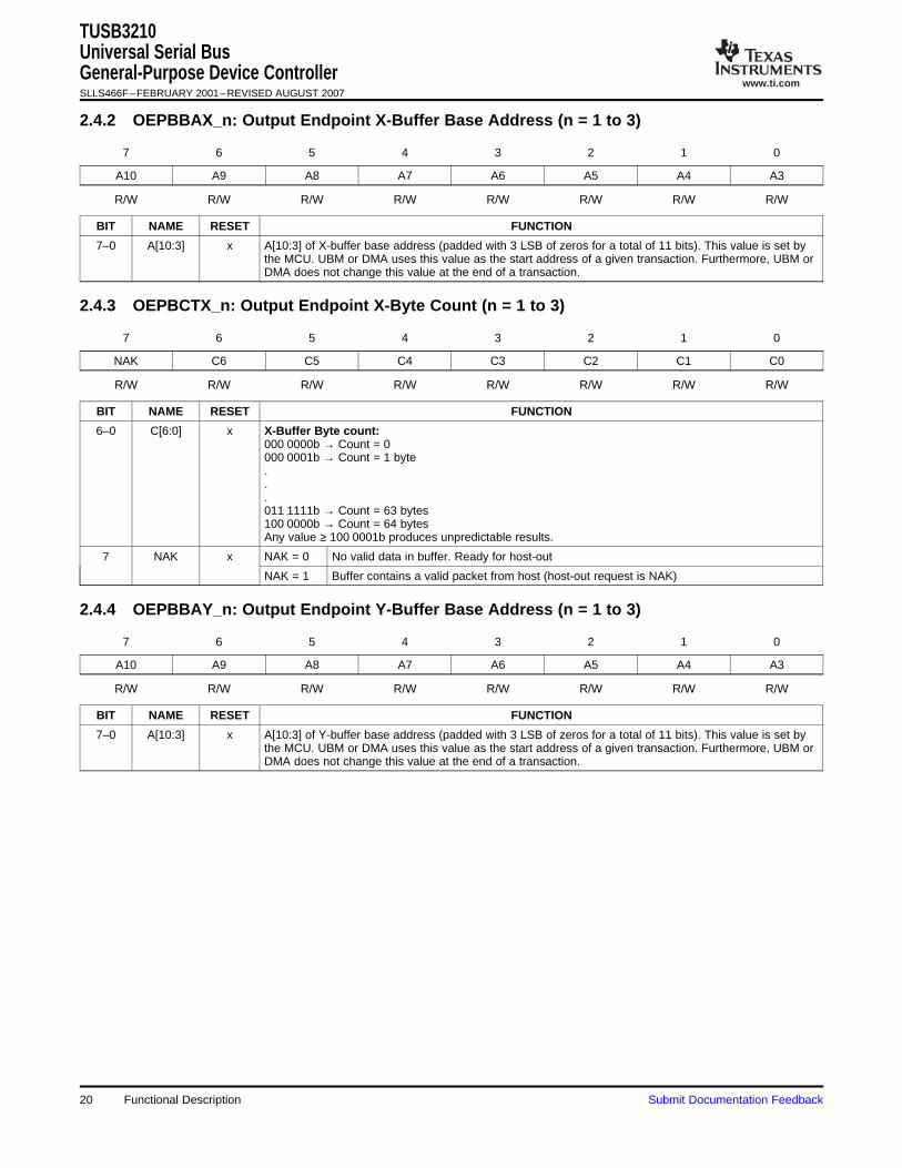
2.4.1 OEPCNF_n: Output Endpoint Configuration (n = 1 to 3)
TUSB3210Universal Serial Bus
General-Purpose Device ControllerSLLS466F–FEBRUARY 2001–REVISED AUGUST 2007
Table 2-4 lists the EDB entries for EDB-1 to EDB-3. EDB-0 registers are described separately.
Table 2-4. EDB Entries in RAM (n = 1 to 3)
Offset ENTRY NAME DESCRIPTION
07 EPSIZXY_n I/O endpoint_n: X/Y buffer size
06 EPBCTY_n I/O endpoint_n: Y byte count
05 EPBBAY_n I/O endpoint_n: Y buffer base address
04 SPARE Not used
03 SPARE Not used
02 EPBCTX_n I/O endpoint_n: X byte count
01 EPBBAX_n I/O endpoint_n: X buffer base address
00 EPCNF_n I/O endpoint_n: configuration
7 6 5 4 3 2 1 0
UBME ISO TOGLE DBUF STALL USBIE RSV RSV
R/W R/W R/W R/W R/W R/W R/O R/O
BIT NAME RESET FUNCTION
1–0 RSV 0 Reserved
2 USBIE x USB interrupt enable on transaction completion. Set/cleared by MCU.
USBIE = 0 No interrupt
USBIE = 1 Interrupt on transaction completion
3 STALL 0 USB stall condition indication. Set/cleared by MCU.
STALL = 0 No stall
STALL = 1 USB stall condition. If set by MCU, a STALL handshake is initiated and the bit is cleared bythe MCU.
4 DBUF x Double buffer enable. Set/cleared by MCU.
DBUF = 0 Primary buffer only (X-buffer only)
DBUF = 1 Toggle bit selects buffer
5 TOGLE x USB toggle bit. This bit reflects the toggle sequence bit of DATA0, DATA1.
6 ISO x ISO = 0 Non-isochronous transfer. This bit must be cleared by the MCU because only non-isochronoustransfer is supported.
7 UBME x UBM enable/disable bit. Set/cleared by the MCU.
UBME = 0 UBM cannot use this endpoint.
UBME = 1 UBM can use this endpoint.
Submit Documentation Feedback Functional Description 19
www.ti.com
2.4.2 OEPBBAX_n: Output Endpoint X-Buffer Base Address (n = 1 to 3)
2.4.3 OEPBCTX_n: Output Endpoint X-Byte Count (n = 1 to 3)
2.4.4 OEPBBAY_n: Output Endpoint Y-Buffer Base Address (n = 1 to 3)
TUSB3210Universal Serial BusGeneral-Purpose Device ControllerSLLS466F–FEBRUARY 2001–REVISED AUGUST 2007
7 6 5 4 3 2 1 0
A10 A9 A8 A7 A6 A5 A4 A3
R/W R/W R/W R/W R/W R/W R/W R/W
BIT NAME RESET FUNCTION
7–0 A[10:3] x A[10:3] of X-buffer base address (padded with 3 LSB of zeros for a total of 11 bits). This value is set bythe MCU. UBM or DMA uses this value as the start address of a given transaction. Furthermore, UBM orDMA does not change this value at the end of a transaction.
7 6 5 4 3 2 1 0
NAK C6 C5 C4 C3 C2 C1 C0
R/W R/W R/W R/W R/W R/W R/W R/W
BIT NAME RESET FUNCTION
6–0 C[6:0] x X-Buffer Byte count:000 0000b → Count = 0000 0001b → Count = 1 byte...011 1111b → Count = 63 bytes100 0000b → Count = 64 bytesAny value ≥ 100 0001b produces unpredictable results.
7 NAK x NAK = 0 No valid data in buffer. Ready for host-out
NAK = 1 Buffer contains a valid packet from host (host-out request is NAK)
7 6 5 4 3 2 1 0
A10 A9 A8 A7 A6 A5 A4 A3
R/W R/W R/W R/W R/W R/W R/W R/W
BIT NAME RESET FUNCTION
7–0 A[10:3] x A[10:3] of Y-buffer base address (padded with 3 LSB of zeros for a total of 11 bits). This value is set bythe MCU. UBM or DMA uses this value as the start address of a given transaction. Furthermore, UBM orDMA does not change this value at the end of a transaction.
Functional Description20 Submit Documentation Feedback
www.ti.com
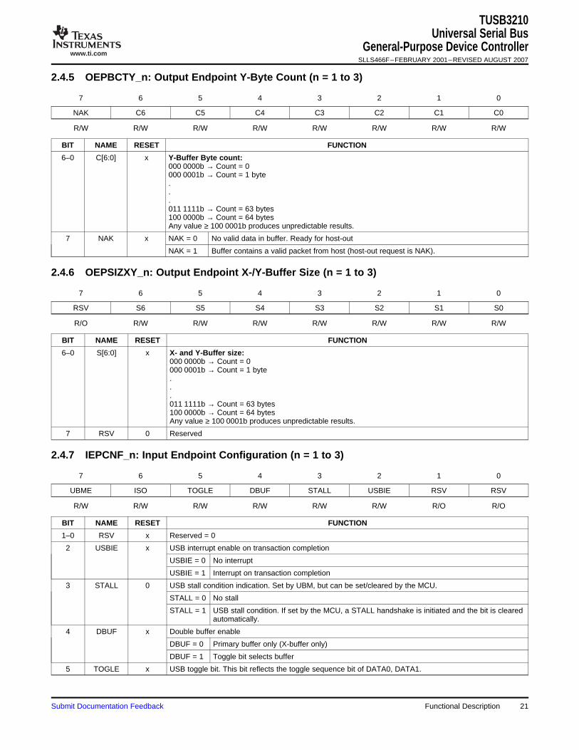
2.4.5 OEPBCTY_n: Output Endpoint Y-Byte Count (n = 1 to 3)
2.4.6 OEPSIZXY_n: Output Endpoint X-/Y-Buffer Size (n = 1 to 3)
2.4.7 IEPCNF_n: Input Endpoint Configuration (n = 1 to 3)
TUSB3210Universal Serial Bus
General-Purpose Device ControllerSLLS466F–FEBRUARY 2001–REVISED AUGUST 2007
7 6 5 4 3 2 1 0
NAK C6 C5 C4 C3 C2 C1 C0
R/W R/W R/W R/W R/W R/W R/W R/W
BIT NAME RESET FUNCTION
6–0 C[6:0] x Y-Buffer Byte count:000 0000b → Count = 0000 0001b → Count = 1 byte...011 1111b → Count = 63 bytes100 0000b → Count = 64 bytesAny value ≥ 100 0001b produces unpredictable results.
7 NAK x NAK = 0 No valid data in buffer. Ready for host-out
NAK = 1 Buffer contains a valid packet from host (host-out request is NAK).
7 6 5 4 3 2 1 0
RSV S6 S5 S4 S3 S2 S1 S0
R/O R/W R/W R/W R/W R/W R/W R/W
BIT NAME RESET FUNCTION
6–0 S[6:0] x X- and Y-Buffer size:000 0000b → Count = 0000 0001b → Count = 1 byte...011 1111b → Count = 63 bytes100 0000b → Count = 64 bytesAny value ≥ 100 0001b produces unpredictable results.
7 RSV 0 Reserved
7 6 5 4 3 2 1 0
UBME ISO TOGLE DBUF STALL USBIE RSV RSV
R/W R/W R/W R/W R/W R/W R/O R/O
BIT NAME RESET FUNCTION
1–0 RSV x Reserved = 0
2 USBIE x USB interrupt enable on transaction completion
USBIE = 0 No interrupt
USBIE = 1 Interrupt on transaction completion
3 STALL 0 USB stall condition indication. Set by UBM, but can be set/cleared by the MCU.
STALL = 0 No stall
STALL = 1 USB stall condition. If set by the MCU, a STALL handshake is initiated and the bit is clearedautomatically.
4 DBUF x Double buffer enable
DBUF = 0 Primary buffer only (X-buffer only)
DBUF = 1 Toggle bit selects buffer
5 TOGLE x USB toggle bit. This bit reflects the toggle sequence bit of DATA0, DATA1.
Submit Documentation Feedback Functional Description 21
www.ti.com
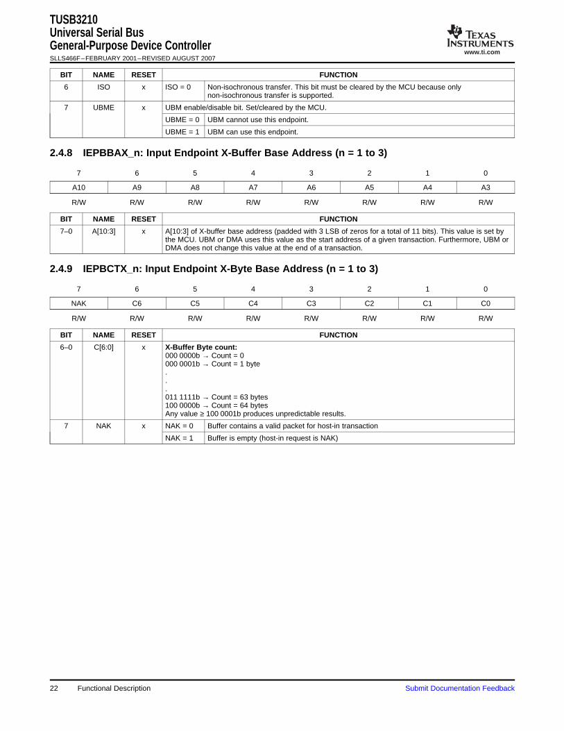
2.4.8 IEPBBAX_n: Input Endpoint X-Buffer Base Address (n = 1 to 3)
2.4.9 IEPBCTX_n: Input Endpoint X-Byte Base Address (n = 1 to 3)
TUSB3210Universal Serial BusGeneral-Purpose Device ControllerSLLS466F–FEBRUARY 2001–REVISED AUGUST 2007
BIT NAME RESET FUNCTION
6 ISO x ISO = 0 Non-isochronous transfer. This bit must be cleared by the MCU because onlynon-isochronous transfer is supported.
7 UBME x UBM enable/disable bit. Set/cleared by the MCU.
UBME = 0 UBM cannot use this endpoint.
UBME = 1 UBM can use this endpoint.
7 6 5 4 3 2 1 0
A10 A9 A8 A7 A6 A5 A4 A3
R/W R/W R/W R/W R/W R/W R/W R/W
BIT NAME RESET FUNCTION
7–0 A[10:3] x A[10:3] of X-buffer base address (padded with 3 LSB of zeros for a total of 11 bits). This value is set bythe MCU. UBM or DMA uses this value as the start address of a given transaction. Furthermore, UBM orDMA does not change this value at the end of a transaction.
7 6 5 4 3 2 1 0
NAK C6 C5 C4 C3 C2 C1 C0
R/W R/W R/W R/W R/W R/W R/W R/W
BIT NAME RESET FUNCTION
6–0 C[6:0] x X-Buffer Byte count:000 0000b → Count = 0000 0001b → Count = 1 byte...011 1111b → Count = 63 bytes100 0000b → Count = 64 bytesAny value ≥ 100 0001b produces unpredictable results.
7 NAK x NAK = 0 Buffer contains a valid packet for host-in transaction
NAK = 1 Buffer is empty (host-in request is NAK)
Functional Description22 Submit Documentation Feedback
www.ti.com
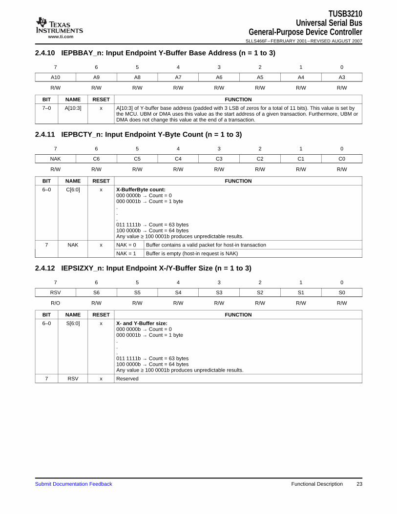
2.4.10 IEPBBAY_n: Input Endpoint Y-Buffer Base Address (n = 1 to 3)
2.4.11 IEPBCTY_n: Input Endpoint Y-Byte Count (n = 1 to 3)
2.4.12 IEPSIZXY_n: Input Endpoint X-/Y-Buffer Size (n = 1 to 3)
TUSB3210Universal Serial Bus
General-Purpose Device ControllerSLLS466F–FEBRUARY 2001–REVISED AUGUST 2007
7 6 5 4 3 2 1 0
A10 A9 A8 A7 A6 A5 A4 A3
R/W R/W R/W R/W R/W R/W R/W R/W
BIT NAME RESET FUNCTION
7–0 A[10:3] x A[10:3] of Y-buffer base address (padded with 3 LSB of zeros for a total of 11 bits). This value is set bythe MCU. UBM or DMA uses this value as the start address of a given transaction. Furthermore, UBM orDMA does not change this value at the end of a transaction.
7 6 5 4 3 2 1 0
NAK C6 C5 C4 C3 C2 C1 C0
R/W R/W R/W R/W R/W R/W R/W R/W
BIT NAME RESET FUNCTION
6–0 C[6:0] x X-BufferByte count:000 0000b → Count = 0000 0001b → Count = 1 byte...011 1111b → Count = 63 bytes100 0000b → Count = 64 bytesAny value ≥ 100 0001b produces unpredictable results.
7 NAK x NAK = 0 Buffer contains a valid packet for host-in transaction
NAK = 1 Buffer is empty (host-in request is NAK)
7 6 5 4 3 2 1 0
RSV S6 S5 S4 S3 S2 S1 S0
R/O R/W R/W R/W R/W R/W R/W R/W
BIT NAME RESET FUNCTION
6–0 S[6:0] x X- and Y-Buffer size:000 0000b → Count = 0000 0001b → Count = 1 byte...011 1111b → Count = 63 bytes100 0000b → Count = 64 bytesAny value ≥ 100 0001b produces unpredictable results.
7 RSV x Reserved
Submit Documentation Feedback Functional Description 23
www.ti.com
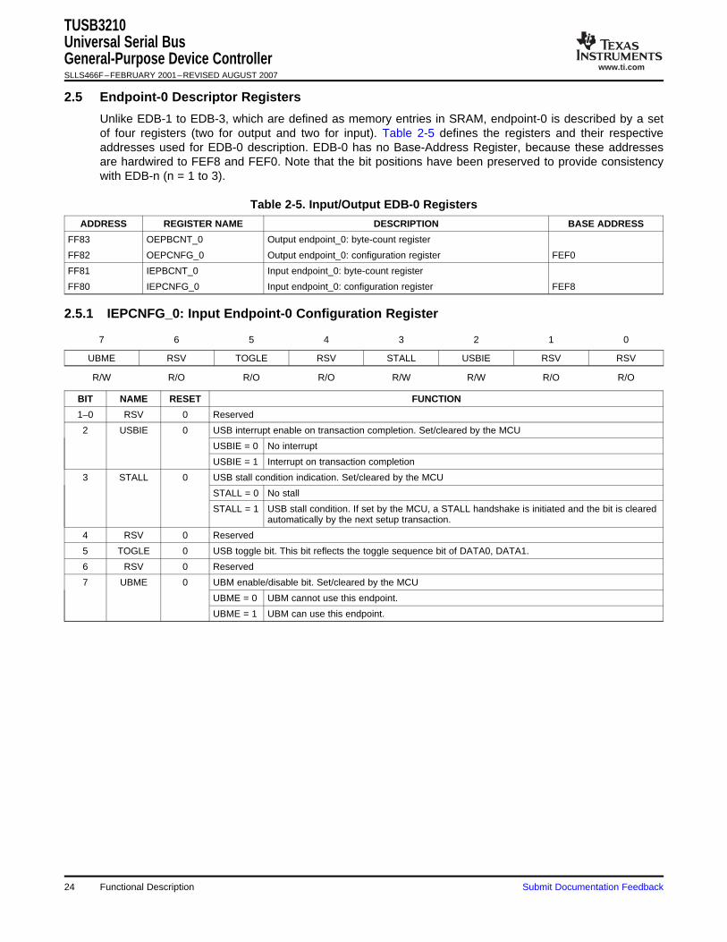
2.5 Endpoint-0 Descriptor Registers
2.5.1 IEPCNFG_0: Input Endpoint-0 Configuration Register
TUSB3210Universal Serial BusGeneral-Purpose Device ControllerSLLS466F–FEBRUARY 2001–REVISED AUGUST 2007
Unlike EDB-1 to EDB-3, which are defined as memory entries in SRAM, endpoint-0 is described by a setof four registers (two for output and two for input). Table 2-5 defines the registers and their respectiveaddresses used for EDB-0 description. EDB-0 has no Base-Address Register, because these addressesare hardwired to FEF8 and FEF0. Note that the bit positions have been preserved to provide consistencywith EDB-n (n = 1 to 3).
Table 2-5. Input/Output EDB-0 Registers
ADDRESS REGISTER NAME DESCRIPTION BASE ADDRESS
FF83 OEPBCNT_0 Output endpoint_0: byte-count register
FF82 OEPCNFG_0 Output endpoint_0: configuration register FEF0
FF81 IEPBCNT_0 Input endpoint_0: byte-count register
FF80 IEPCNFG_0 Input endpoint_0: configuration register FEF8
7 6 5 4 3 2 1 0
UBME RSV TOGLE RSV STALL USBIE RSV RSV
R/W R/O R/O R/O R/W R/W R/O R/O
BIT NAME RESET FUNCTION
1–0 RSV 0 Reserved
2 USBIE 0 USB interrupt enable on transaction completion. Set/cleared by the MCU
USBIE = 0 No interrupt
USBIE = 1 Interrupt on transaction completion
3 STALL 0 USB stall condition indication. Set/cleared by the MCU
STALL = 0 No stall
STALL = 1 USB stall condition. If set by the MCU, a STALL handshake is initiated and the bit is clearedautomatically by the next setup transaction.
4 RSV 0 Reserved
5 TOGLE 0 USB toggle bit. This bit reflects the toggle sequence bit of DATA0, DATA1.
6 RSV 0 Reserved
7 UBME 0 UBM enable/disable bit. Set/cleared by the MCU
UBME = 0 UBM cannot use this endpoint.
UBME = 1 UBM can use this endpoint.
24 Functional Description Submit Documentation Feedback
www.ti.com
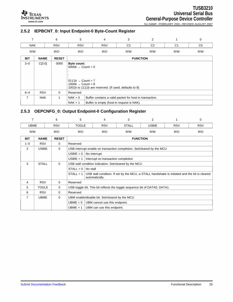
2.5.2 IEPBCNT_0: Input Endpoint-0 Byte-Count Register
2.5.3 OEPCNFG_0: Output Endpoint-0 Configuration Register
TUSB3210Universal Serial Bus
General-Purpose Device ControllerSLLS466F–FEBRUARY 2001–REVISED AUGUST 2007
7 6 5 4 3 2 1 0
NAK RSV RSV RSV C3 C2 C1 C0
R/W R/O R/O R/O R/W R/W R/W R/W
BIT NAME RESET FUNCTION
3–0 C[3:0] 0000 Byte count:0000b → Count = 0...0111b → Count = 71000b → Count = 81001b to 1111b are reserved. (If used, defaults to 8)
6–4 RSV 0 Reserved
7 NAK 1 NAK = 0 Buffer contains a valid packet for host-in transaction.
NAK = 1 Buffer is empty (host-in request is NAK).
7 6 5 4 3 2 1 0
UBME RSV TOGLE RSV STALL USBIE RSV RSV
R/W R/O R/O R/O R/W R/W R/O R/O
BIT NAME RESET FUNCTION
1–0 RSV 0 Reserved
2 USBIE 0 USB interrupt enable on transaction completion. Set/cleared by the MCU
USBIE = 0 No interrupt
USBIE = 1 Interrupt on transaction completion
3 STALL 0 USB stall condition indication. Set/cleared by the MCU
STALL = 0 No stall
STALL = 1 USB stall condition. If set by the MCU, a STALL handshake is initiated and the bit is clearedautomatically.
4 RSV 0 Reserved
5 TOGLE 0 USB toggle bit. This bit reflects the toggle sequence bit of DATA0, DATA1.
6 RSV 0 Reserved
7 UBME 0 UBM enable/disable bit. Set/cleared by the MCU
UBME = 0 UBM cannot use this endpoint.
UBME = 1 UBM can use this endpoint.
Submit Documentation Feedback Functional Description 25
www.ti.com
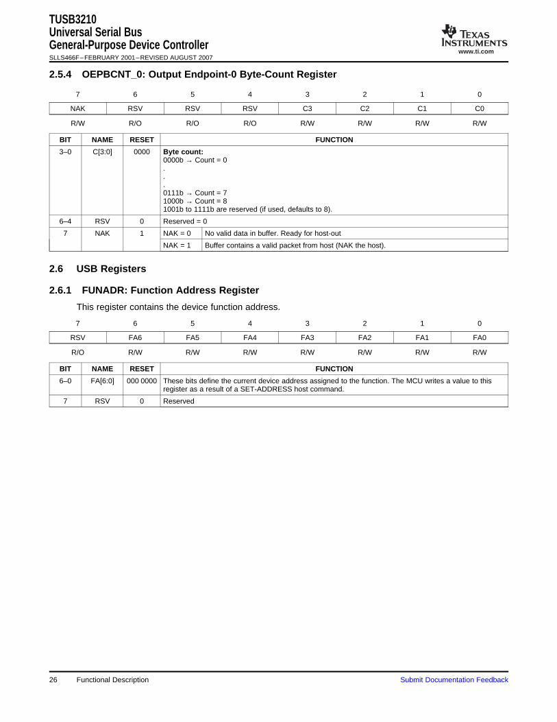
2.5.4 OEPBCNT_0: Output Endpoint-0 Byte-Count Register
2.6 USB Registers
2.6.1 FUNADR: Function Address Register
TUSB3210Universal Serial BusGeneral-Purpose Device ControllerSLLS466F–FEBRUARY 2001–REVISED AUGUST 2007
7 6 5 4 3 2 1 0
NAK RSV RSV RSV C3 C2 C1 C0
R/W R/O R/O R/O R/W R/W R/W R/W
BIT NAME RESET FUNCTION
3–0 C[3:0] 0000 Byte count:0000b → Count = 0...0111b → Count = 71000b → Count = 81001b to 1111b are reserved (if used, defaults to 8).
6–4 RSV 0 Reserved = 0
7 NAK 1 NAK = 0 No valid data in buffer. Ready for host-out
NAK = 1 Buffer contains a valid packet from host (NAK the host).
This register contains the device function address.
7 6 5 4 3 2 1 0
RSV FA6 FA5 FA4 FA3 FA2 FA1 FA0
R/O R/W R/W R/W R/W R/W R/W R/W
BIT NAME RESET FUNCTION
6–0 FA[6:0] 000 0000 These bits define the current device address assigned to the function. The MCU writes a value to thisregister as a result of a SET-ADDRESS host command.
7 RSV 0 Reserved
Functional Description26 Submit Documentation Feedback
www.ti.com
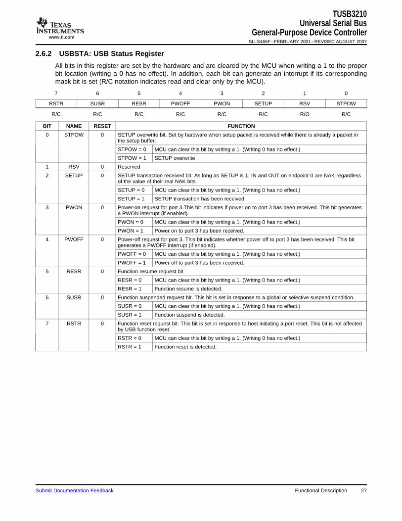
2.6.2 USBSTA: USB Status Register
TUSB3210Universal Serial Bus
General-Purpose Device ControllerSLLS466F–FEBRUARY 2001–REVISED AUGUST 2007
All bits in this register are set by the hardware and are cleared by the MCU when writing a 1 to the properbit location (writing a 0 has no effect). In addition, each bit can generate an interrupt if its correspondingmask bit is set (R/C notation indicates read and clear only by the MCU).
7 6 5 4 3 2 1 0
RSTR SUSR RESR PWOFF PWON SETUP RSV STPOW
R/C R/C R/C R/C R/C R/C R/O R/C
BIT NAME RESET FUNCTION
0 STPOW 0 SETUP overwrite bit. Set by hardware when setup packet is received while there is already a packet inthe setup buffer.
STPOW = 0 MCU can clear this bit by writing a 1. (Writing 0 has no effect.)
STPOW = 1 SETUP overwrite
1 RSV 0 Reserved
2 SETUP 0 SETUP transaction received bit. As long as SETUP is 1, IN and OUT on endpoint-0 are NAK regardlessof the value of their real NAK bits.
SETUP = 0 MCU can clear this bit by writing a 1. (Writing 0 has no effect.)
SETUP = 1 SETUP transaction has been received.
3 PWON 0 Power-on request for port 3.This bit indicates if power on to port 3 has been received. This bit generatesa PWON interrupt (if enabled).
PWON = 0 MCU can clear this bit by writing a 1. (Writing 0 has no effect.)
PWON = 1 Power on to port 3 has been received.
4 PWOFF 0 Power-off request for port 3. This bit indicates whether power off to port 3 has been received. This bitgenerates a PWOFF interrupt (if enabled).
PWOFF = 0 MCU can clear this bit by writing a 1. (Writing 0 has no effect.)
PWOFF = 1 Power off to port 3 has been received.
5 RESR 0 Function resume request bit
RESR = 0 MCU can clear this bit by writing a 1. (Writing 0 has no effect.)
RESR = 1 Function resume is detected.
6 SUSR 0 Function suspended request bit. This bit is set in response to a global or selective suspend condition.
SUSR = 0 MCU can clear this bit by writing a 1. (Writing 0 has no effect.)
SUSR = 1 Function suspend is detected.
7 RSTR 0 Function reset request bit. This bit is set in response to host initiating a port reset. This bit is not affectedby USB function reset.
RSTR = 0 MCU can clear this bit by writing a 1. (Writing 0 has no effect.)
RSTR = 1 Function reset is detected.
Submit Documentation Feedback Functional Description 27
www.ti.com
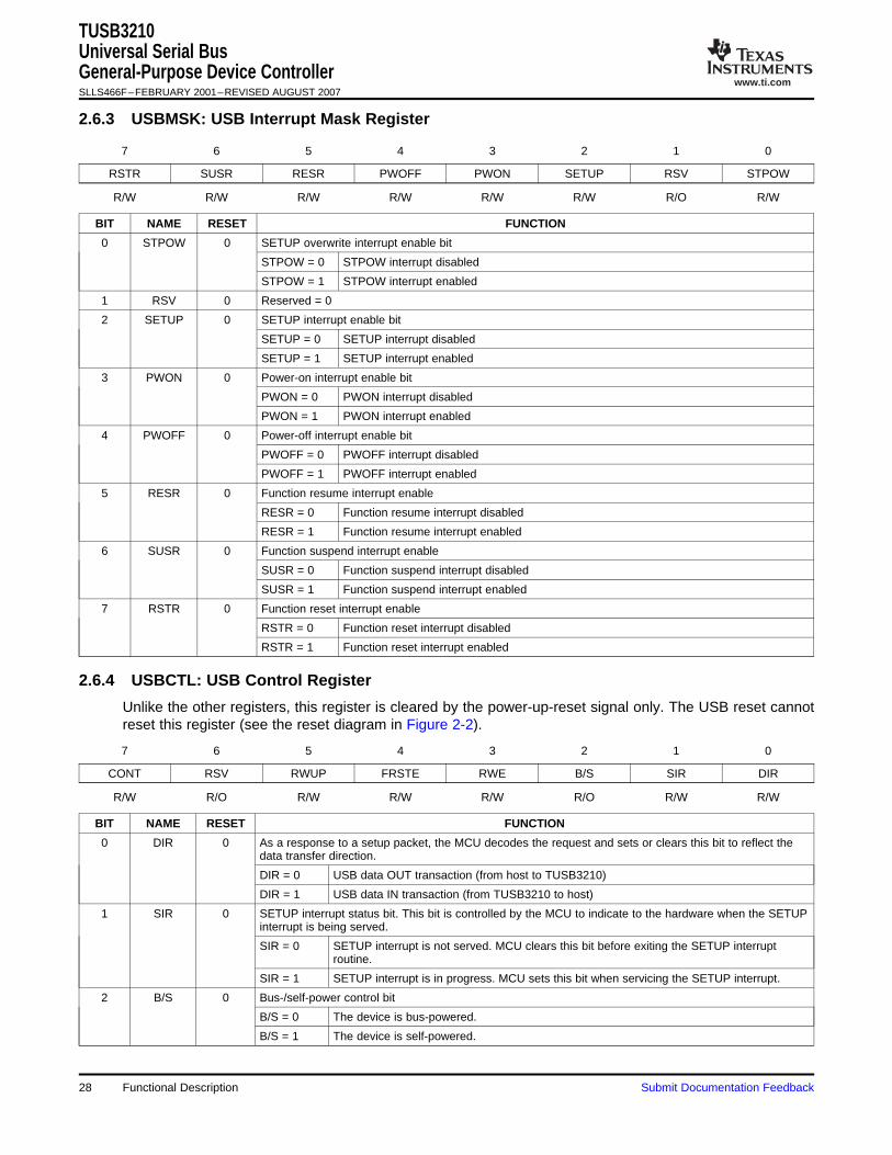
2.6.3 USBMSK: USB Interrupt Mask Register
2.6.4 USBCTL: USB Control Register
TUSB3210Universal Serial BusGeneral-Purpose Device ControllerSLLS466F–FEBRUARY 2001–REVISED AUGUST 2007
7 6 5 4 3 2 1 0
RSTR SUSR RESR PWOFF PWON SETUP RSV STPOW
R/W R/W R/W R/W R/W R/W R/O R/W
BIT NAME RESET FUNCTION
0 STPOW 0 SETUP overwrite interrupt enable bit
STPOW = 0 STPOW interrupt disabled
STPOW = 1 STPOW interrupt enabled
1 RSV 0 Reserved = 0
2 SETUP 0 SETUP interrupt enable bit
SETUP = 0 SETUP interrupt disabled
SETUP = 1 SETUP interrupt enabled
3 PWON 0 Power-on interrupt enable bit
PWON = 0 PWON interrupt disabled
PWON = 1 PWON interrupt enabled
4 PWOFF 0 Power-off interrupt enable bit
PWOFF = 0 PWOFF interrupt disabled
PWOFF = 1 PWOFF interrupt enabled
5 RESR 0 Function resume interrupt enable
RESR = 0 Function resume interrupt disabled
RESR = 1 Function resume interrupt enabled
6 SUSR 0 Function suspend interrupt enable
SUSR = 0 Function suspend interrupt disabled
SUSR = 1 Function suspend interrupt enabled
7 RSTR 0 Function reset interrupt enable
RSTR = 0 Function reset interrupt disabled
RSTR = 1 Function reset interrupt enabled
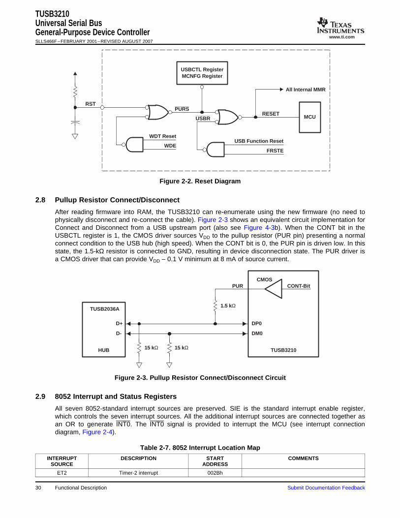
Unlike the other registers, this register is cleared by the power-up-reset signal only. The USB reset cannotreset this register (see the reset diagram in Figure 2-2).
7 6 5 4 3 2 1 0
CONT RSV RWUP FRSTE RWE B/S SIR DIR
R/W R/O R/W R/W R/W R/O R/W R/W
BIT NAME RESET FUNCTION
0 DIR 0 As a response to a setup packet, the MCU decodes the request and sets or clears this bit to reflect thedata transfer direction.
DIR = 0 USB data OUT transaction (from host to TUSB3210)
DIR = 1 USB data IN transaction (from TUSB3210 to host)
1 SIR 0 SETUP interrupt status bit. This bit is controlled by the MCU to indicate to the hardware when the SETUPinterrupt is being served.
SIR = 0 SETUP interrupt is not served. MCU clears this bit before exiting the SETUP interruptroutine.
SIR = 1 SETUP interrupt is in progress. MCU sets this bit when servicing the SETUP interrupt.
2 B/S 0 Bus-/self-power control bit
B/S = 0 The device is bus-powered.
B/S = 1 The device is self-powered.
Functional Description28 Submit Documentation Feedback
www.ti.com
2.6.5 VIDSTA: VID/PID Status Register
2.7 Function Reset and Power-Up Reset Interconnect
TUSB3210Universal Serial Bus
General-Purpose Device ControllerSLLS466F–FEBRUARY 2001–REVISED AUGUST 2007
BIT NAME RESET FUNCTION
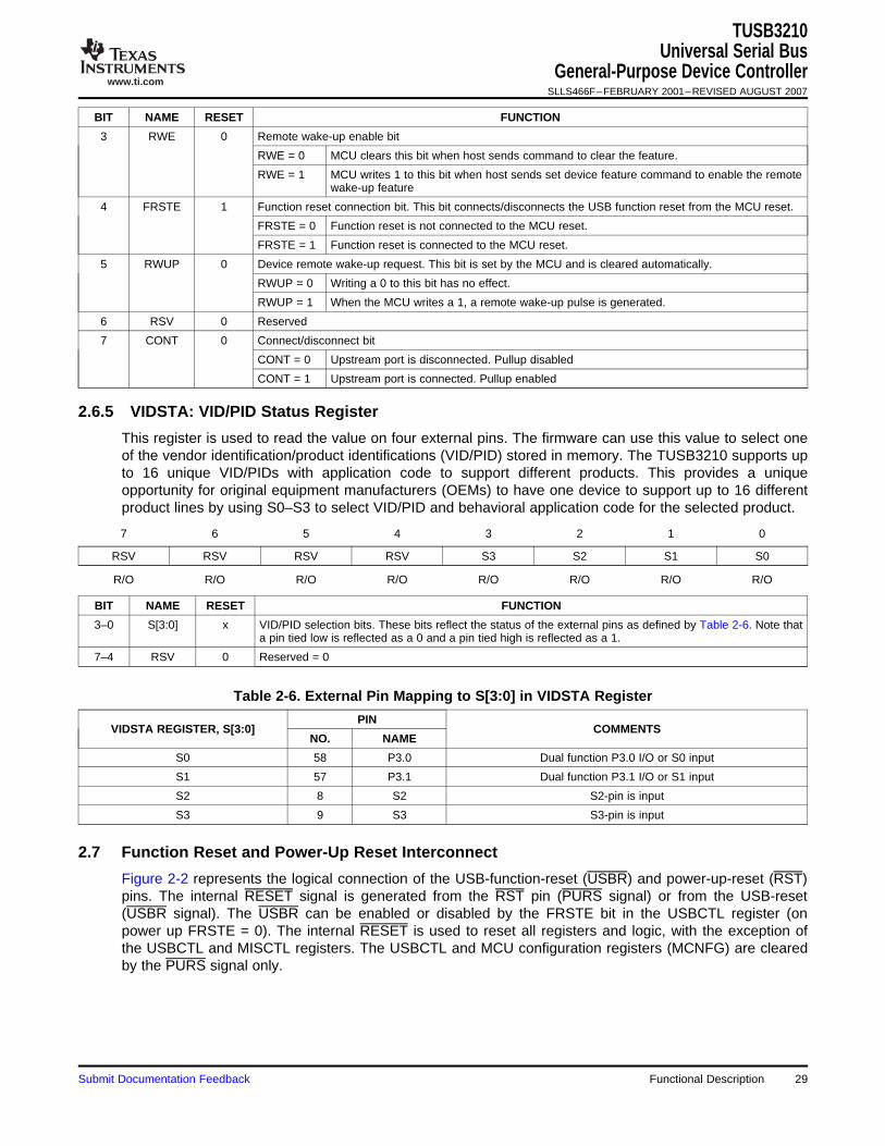
3 RWE 0 Remote wake-up enable bit
RWE = 0 MCU clears this bit when host sends command to clear the feature.
RWE = 1 MCU writes 1 to this bit when host sends set device feature command to enable the remotewake-up feature
4 FRSTE 1 Function reset connection bit. This bit connects/disconnects the USB function reset from the MCU reset.
FRSTE = 0 Function reset is not connected to the MCU reset.
FRSTE = 1 Function reset is connected to the MCU reset.
5 RWUP 0 Device remote wake-up request. This bit is set by the MCU and is cleared automatically.
RWUP = 0 Writing a 0 to this bit has no effect.
RWUP = 1 When the MCU writes a 1, a remote wake-up pulse is generated.
6 RSV 0 Reserved
7 CONT 0 Connect/disconnect bit
CONT = 0 Upstream port is disconnected. Pullup disabled
CONT = 1 Upstream port is connected. Pullup enabled
This register is used to read the value on four external pins. The firmware can use this value to select oneof the vendor identification/product identifications (VID/PID) stored in memory. The TUSB3210 supports upto 16 unique VID/PIDs with application code to support different products. This provides a uniqueopportunity for original equipment manufacturers (OEMs) to have one device to support up to 16 differentproduct lines by using S0–S3 to select VID/PID and behavioral application code for the selected product.
7 6 5 4 3 2 1 0
RSV RSV RSV RSV S3 S2 S1 S0
R/O R/O R/O R/O R/O R/O R/O R/O
BIT NAME RESET FUNCTION
3–0 S[3:0] x VID/PID selection bits. These bits reflect the status of the external pins as defined by Table 2-6. Note thata pin tied low is reflected as a 0 and a pin tied high is reflected as a 1.
7–4 RSV 0 Reserved = 0
Table 2-6. External Pin Mapping to S[3:0] in VIDSTA Register
PINVIDSTA REGISTER, S[3:0] COMMENTS
NO. NAME
S0 58 P3.0 Dual function P3.0 I/O or S0 input
S1 57 P3.1 Dual function P3.1 I/O or S1 input
S2 8 S2 S2-pin is input
S3 9 S3 S3-pin is input
Figure 2-2 represents the logical connection of the USB-function-reset (USBR) and power-up-reset (RST)pins. The internal RESET signal is generated from the RST pin (PURS signal) or from the USB-reset(USBR signal). The USBR can be enabled or disabled by the FRSTE bit in the USBCTL register (onpower up FRSTE = 0). The internal RESET is used to reset all registers and logic, with the exception ofthe USBCTL and MISCTL registers. The USBCTL and MCU configuration registers (MCNFG) are clearedby the PURS signal only.
Submit Documentation Feedback Functional Description 29
www.ti.com
WDT Reset
WDE
PURS
USBCTL RegisterMCNFG Register
USB Function Reset
FRSTE
RESETMCU
All Internal MMR
RST
USBR
2.8 Pullup Resistor Connect/Disconnect
D+
TUSB3210
DM0
DP0
CMOSCONT-BitPUR
1.5 kΩ
15 kΩ15 kΩHUB
D-
TUSB2036A
2.9 8052 Interrupt and Status Registers
TUSB3210Universal Serial BusGeneral-Purpose Device ControllerSLLS466F–FEBRUARY 2001–REVISED AUGUST 2007
Figure 2-2. Reset Diagram
After reading firmware into RAM, the TUSB3210 can re-enumerate using the new firmware (no need tophysically disconnect and re-connect the cable). Figure 2-3 shows an equivalent circuit implementation forConnect and Disconnect from a USB upstream port (also see Figure 4-3b). When the CONT bit in theUSBCTL register is 1, the CMOS driver sources VDD to the pullup resistor (PUR pin) presenting a normalconnect condition to the USB hub (high speed). When the CONT bit is 0, the PUR pin is driven low. In thisstate, the 1.5-kΩ resistor is connected to GND, resulting in device disconnection state. The PUR driver isa CMOS driver that can provide VDD – 0.1 V minimum at 8 mA of source current.
Figure 2-3. Pullup Resistor Connect/Disconnect Circuit
All seven 8052-standard interrupt sources are preserved. SIE is the standard interrupt enable register,which controls the seven interrupt sources. All the additional interrupt sources are connected together asan OR to generate INT0. The INT0 signal is provided to interrupt the MCU (see interrupt connectiondiagram, Figure 2-4).
Table 2-7. 8052 Interrupt Location Map
INTERRUPT DESCRIPTION START COMMENTSSOURCE ADDRESS
ET2 Timer-2 interrupt 002Bh
Functional Description30 Submit Documentation Feedback
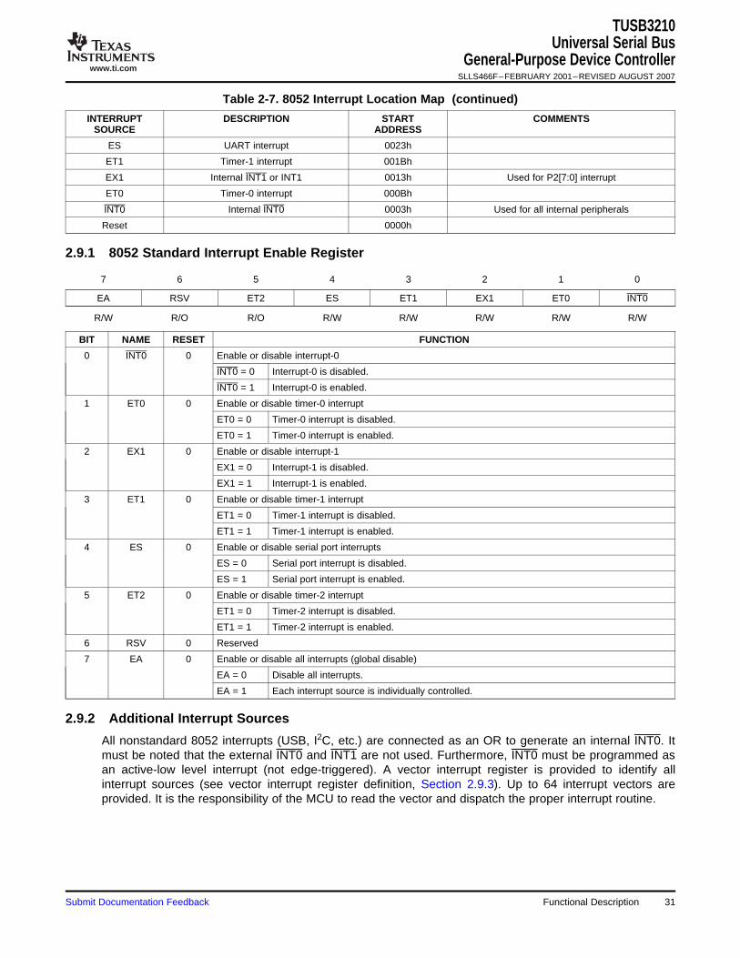
www.ti.com
2.9.1 8052 Standard Interrupt Enable Register
2.9.2 Additional Interrupt Sources
TUSB3210Universal Serial Bus
General-Purpose Device ControllerSLLS466F–FEBRUARY 2001–REVISED AUGUST 2007
Table 2-7. 8052 Interrupt Location Map (continued)
INTERRUPT DESCRIPTION START COMMENTSSOURCE ADDRESS
ES UART interrupt 0023h
ET1 Timer-1 interrupt 001Bh
EX1 Internal INT1 or INT1 0013h Used for P2[7:0] interrupt
ET0 Timer-0 interrupt 000Bh
INT0 Internal INT0 0003h Used for all internal peripherals
Reset 0000h
7 6 5 4 3 2 1 0
EA RSV ET2 ES ET1 EX1 ET0 INT0
R/W R/O R/O R/W R/W R/W R/W R/W
BIT NAME RESET FUNCTION
0 INT0 0 Enable or disable interrupt-0
INT0 = 0 Interrupt-0 is disabled.
INT0 = 1 Interrupt-0 is enabled.
1 ET0 0 Enable or disable timer-0 interrupt
ET0 = 0 Timer-0 interrupt is disabled.
ET0 = 1 Timer-0 interrupt is enabled.
2 EX1 0 Enable or disable interrupt-1
EX1 = 0 Interrupt-1 is disabled.
EX1 = 1 Interrupt-1 is enabled.
3 ET1 0 Enable or disable timer-1 interrupt
ET1 = 0 Timer-1 interrupt is disabled.
ET1 = 1 Timer-1 interrupt is enabled.
4 ES 0 Enable or disable serial port interrupts
ES = 0 Serial port interrupt is disabled.
ES = 1 Serial port interrupt is enabled.
5 ET2 0 Enable or disable timer-2 interrupt
ET1 = 0 Timer-2 interrupt is disabled.
ET1 = 1 Timer-2 interrupt is enabled.
6 RSV 0 Reserved
7 EA 0 Enable or disable all interrupts (global disable)
EA = 0 Disable all interrupts.
EA = 1 Each interrupt source is individually controlled.
All nonstandard 8052 interrupts (USB, I2C, etc.) are connected as an OR to generate an internal INT0. Itmust be noted that the external INT0 and INT1 are not used. Furthermore, INT0 must be programmed asan active-low level interrupt (not edge-triggered). A vector interrupt register is provided to identify allinterrupt sources (see vector interrupt register definition, Section 2.9.3). Up to 64 interrupt vectors areprovided. It is the responsibility of the MCU to read the vector and dispatch the proper interrupt routine.
Submit Documentation Feedback Functional Description 31
www.ti.com
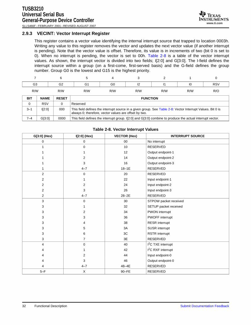
2.9.3 VECINT: Vector Interrupt Register
TUSB3210Universal Serial BusGeneral-Purpose Device ControllerSLLS466F–FEBRUARY 2001–REVISED AUGUST 2007
This register contains a vector value identifying the internal interrupt source that trapped to location 0003h.Writing any value to this register removes the vector and updates the next vector value (if another interruptis pending). Note that the vector value is offset. Therefore, its value is in increments of two (bit 0 is set to0). When no interrupt is pending, the vector is set to 00h. Table 2-8 is a table of the vector interruptvalues. As shown, the interrupt vector is divided into two fields; I[2:0] and G[3:0]. The I-field defines theinterrupt source within a group (on a first-come, first-served basis) and the G-field defines the groupnumber. Group G0 is the lowest and G15 is the highest priority.
7 6 5 4 3 2 1 0
G3 G2 G1 G0 I2 I1 I0 RSV
R/W R/W R/W R/W R/W R/W R/W R/O
BIT NAME RESET FUNCTION
0 RSV 0 Reserved
3–1 I[2:0] 000 This field defines the interrupt source in a given group. See Table 2-8: Vector Interrupt Values. Bit 0 isalways 0; therefore, vector values are offset by two.
7–4 G[3:0] 0000 This field defines the interrupt group. I[2:0] and G[3:0] combine to produce the actual interrupt vector.
Table 2-8. Vector Interrupt Values
G[3:0] (Hex) I[2:0] (Hex) VECTOR (Hex) INTERRUPT SOURCE
0 0 00 No interrupt
1 0 10 RESERVED
1 1 12 Output endpoint-1
1 2 14 Output endpoint-2
1 3 16 Output endpoint-3
1 4–7 18–1E RESERVED
2 0 20 RESERVED
2 1 22 Input endpoint-1
2 2 24 Input endpoint-2
2 3 26 Input endpoint-3
2 4–7 28–2E RESERVED
3 0 30 STPOW packet received
3 1 32 SETUP packet received
3 2 34 PWON interrupt
3 3 36 PWOFF interrupt
3 4 38 RESR interrupt
3 5 3A SUSR interrupt
3 6 3C RSTR interrupt
3 7 3E RESERVED
4 0 40 I2C TXE interrupt
4 1 42 I2C RXF interrupt
4 2 44 Input endpoint-0
4 3 46 Output endpoint-0
4 4–7 48–4E RESERVED
5–F X 90–FE RESERVED
Functional Description32 Submit Documentation Feedback
www.ti.com
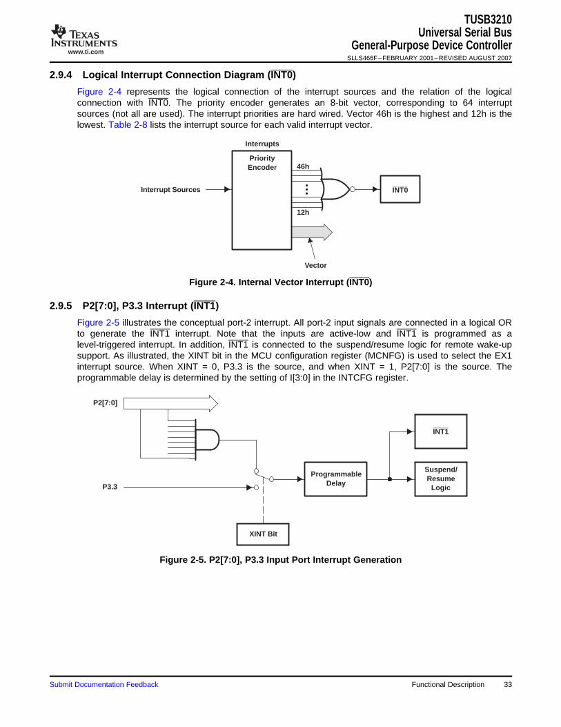
2.9.4 Logical Interrupt Connection Diagram (INT0)
Interrupts
INT0
PriorityEncoder
Vector
Interrupt Sources
46h
12h
2.9.5 P2[7:0], P3.3 Interrupt (INT1)
Suspend/Resume
Logic
P2[7:0]
P3.3
INT1
XINT Bit
ProgrammableDelay
TUSB3210Universal Serial Bus
General-Purpose Device ControllerSLLS466F–FEBRUARY 2001–REVISED AUGUST 2007
Figure 2-4 represents the logical connection of the interrupt sources and the relation of the logicalconnection with INT0. The priority encoder generates an 8-bit vector, corresponding to 64 interruptsources (not all are used). The interrupt priorities are hard wired. Vector 46h is the highest and 12h is thelowest. Table 2-8 lists the interrupt source for each valid interrupt vector.
Figure 2-4. Internal Vector Interrupt (INT0)
Figure 2-5 illustrates the conceptual port-2 interrupt. All port-2 input signals are connected in a logical ORto generate the INT1 interrupt. Note that the inputs are active-low and INT1 is programmed as alevel-triggered interrupt. In addition, INT1 is connected to the suspend/resume logic for remote wake-upsupport. As illustrated, the XINT bit in the MCU configuration register (MCNFG) is used to select the EX1interrupt source. When XINT = 0, P3.3 is the source, and when XINT = 1, P2[7:0] is the source. Theprogrammable delay is determined by the setting of I[3:0] in the INTCFG register.
Figure 2-5. P2[7:0], P3.3 Input Port Interrupt Generation
Submit Documentation Feedback Functional Description 33
www.ti.com
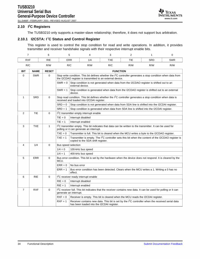
2.10 I2C Registers
2.10.1 I2CSTA: I 2C Status and Control Register
TUSB3210Universal Serial BusGeneral-Purpose Device ControllerSLLS466F–FEBRUARY 2001–REVISED AUGUST 2007
The TUSB3210 only supports a master-slave relationship; therefore, it does not support bus arbitration.
This register is used to control the stop condition for read and write operations. In addition, it providestransmitter and receiver handshake signals with their respective interrupt enable bits.
7 6 5 4 3 2 1 0
RXF RIE ERR 1/4 TXE TIE SRD SWR
R/C R/W R/C R/W R/C R/W R/W R/W
BIT NAME RESET FUNCTION
0 SWR 0 Stop write condition. This bit defines whether the I2C controller generates a stop condition when data fromthe I2CDAO register is transmitted to an external device.
SWR = 0 Stop condition is not generated when data from the I2CDAO register is shifted out to anexternal device.
SWR = 1 Stop condition is generated when data from the I2CDAO register is shifted out to an externaldevice.
1 SRD 0 Stop read condition. This bit defines whether the I2C controller generates a stop condition when data isreceived and loaded into I2CDAI register.
SRD = 0 Stop condition is not generated when data from SDA line is shifted into the I2CDAI register.
SRD = 1 Stop condition is generated when data from SDA line is shifted into the I2CDAI register.
2 TIE 0 I2C transmitter empty interrupt enable
TIE = 0 Interrupt disabled
TIE = 1 Interrupt enabled
3 TXE 1 I2C transmitter empty. This bit indicates that data can be written to the transmitter. It can be used forpolling or it can generate an interrupt.
TXE = 0 Transmitter is full. This bit is cleared when the MCU writes a byte to the I2CDAO register.
TXE = 1 Transmitter is empty. The I2C controller sets this bit when the content of the I2CDAO register iscopied to the SDA shift register.
4 1/4 0 Bus speed selection
1/4 = 0 100-kHz bus speed
1/4 = 1 400-kHz bus speed
5 ERR 0 Bus error condition. This bit is set by the hardware when the device does not respond. It is cleared by theMCU.
ERR = 0 No bus error
ERR = 1 Bus error condition has been detected. Clears when the MCU writes a 1. Writing a 0 has noeffect.
6 RIE 0 I2C receiver ready interrupt enable
RIE = 0 Interrupt disabled
RIE = 1 Interrupt enabled
7 RXF 0 I2C receiver full. This bit indicates that the receiver contains new data. It can be used for polling or it cangenerate an interrupt.
RXF = 0 Receiver is empty. This bit is cleared when the MCU reads the I2CDAI register.
RXF = 1 Receiver contains new data. This bit is set by the I2C controller when the received serial datahas been loaded into the I2CDAI register.
Functional Description34 Submit Documentation Feedback
www.ti.com
2.10.2 I2CADR: I2C Address Register
2.10.3 I2CDAI: I2C Data-Input Register
2.10.4 I2CDAO: I2C Data-Output Register
2.11 Read/Write Operations
2.11.1 Read Operation (Serial EEPROM)
TUSB3210Universal Serial Bus
General-Purpose Device ControllerSLLS466F–FEBRUARY 2001–REVISED AUGUST 2007
This register holds the device address and the read/write command bit.
7 6 5 4 3 2 1 0
A6 A5 A4 A3 A2 A1 A0 R/W
R/W R/W R/W R/W R/W R/W R/W R/W
BIT NAME RESET FUNCTION
0 R/W 0 Read/write command bit
R/W = 0 Write operation
R/W = 1 Read operation
7–1 A[6:0] 000 0000 Seven address bits for device addressing
This register holds the received data from an external device.
7 6 5 4 3 2 1 0
D7 D6 D5 D4 D3 D2 D1 D0
R/O R/O R/O R/O R/O R/O R/O R/O
BIT NAME RESET FUNCTION
7–0 D[7:0] 0 8-bit input data from an I2C device
This register holds the data to be transmitted to an external device. Writing to this register starts thetransfer on the SDA line.
7 6 5 4 3 2 1 0
D7 D6 D5 D4 D3 D2 D1 D0
R/W R/W R/W R/W R/W R/W R/W R/W
BIT NAME RESET FUNCTION
7–0 D[7:0] 0 8-bit output data to an I2C device
A serial read requires a dummy byte write sequence to load in the 16-bit data word address. Once thedevice address word and data address word are clocked out and acknowledged by the device, the MCUstarts a current address sequence. The following describes the sequence of events to accomplish thistransaction:
Device Address + EEPROM [High Byte]
1. The MCU sets I2CSTA[SRD] = 0.This prevents the I2C controller from generating a stop condition afterthe content of the I2CDAI register is received.
2. The MCU sets I2CSTA[SWR] = 0. This prevents the I2C controller from generating a stop conditionafter the content of the I2CDAO register is transmitted.
3. The MCU writes the device address (R/W bit = 0) to the I2CADR register (write operation).
4. The MCU writes the high byte of the EEPROM address into the I2CDAO register, starting the transferon the SDA line.
5. The TXE bit in I2CSTA is cleared, indicating busy.
6. The content of the I2CADR register is transmitted to the EEPROM (preceded by start condition on
Submit Documentation Feedback Functional Description 35
www.ti.com
2.11.2 Current Address Read Operation
2.11.3 Sequential Read Operation
TUSB3210Universal Serial BusGeneral-Purpose Device ControllerSLLS466F–FEBRUARY 2001–REVISED AUGUST 2007
SDA).
7. The content of the I2CDAO register is transmitted to the EEPROM (EEPROM address).
8. The TXE bit in I2CSTA is set, and interrupts the MCU, indicating that the I2CDAO register has beentransmitted.
9. No stop condition is generated.
EEPROM [Low Byte]
1. The MCU writes the low byte of the EEPROM address into the I2CDAO register.
2. The TXE bit in I2CSTA is cleared, indicating busy.
3. The content of the I2CDAO register is transmitted to the device (EEPROM address).
4. The TXE bit in I2CSTA is set, and interrupts the MCU, indicating that the I2CDAO register has beentransmitted.
5. This completes the dummy write operation. At this point, the EEPROM address is set and the MCUcan do a single or a sequential read operation.
Once the EEPROM address is set, the MCU can read a single byte by executing the following steps:
1. The MCU sets I2CSTA[SRD] = 1, forcing the I2C controller to generate a stop condition after theI2CDAI register is received.
2. The MCU writes the device address (R/W bit = 1) to the I2CADR register (read operation).
3. The MCU writes a dummy byte to the I2CDAO register, starting the transfer on the SDA line.
4. The RXF bit in I2CSTA is cleared.
5. The content of the I2CADR register is transmitted to the device, preceded by a start condition on SDA.
6. Data from the EEPROM is latched into the I2CDAI register (stop condition is transmitted).
7. The RXF bit in I2CSTA is set, and interrupts the MCU, indicating that the data is available.
8. The MCU reads the I2CDAI register. This clears the RXF bit (I2CSTA[RXF] = 0).
Once the EEPROM address is set, the MCU can execute a sequential read operation by executing thefollowing steps (Note: this example illustrates a 32-byte sequential read):
1. Device Address
a. The MCU sets I2CSTA[SRD] = 0. This prevents the I2C controller from generating a stop conditionafter the I2CDAI register is received.
b. The MCU writes the device address (R/W bit = 1) to the I2CADR register (read operation).c. The MCU writes a dummy byte to the I2CDAO register, starting the transfer on the SDA line.d. The RXF bit in I2CSTA is cleared.e. The content of the I2CADR register is transmitted to the device (preceded by a start condition on
SDA).
2. N-Byte Read (31 bytes)
a. Data from the device is latched into the I2CDAI register (stop condition is not transmitted).b. The RXF bit in I2CSTA is set and interrupts the MCU, indicating that data is available.c. The MCU reads the I2CDAI register, clearing the RXF bit (I2CSTA[RXF] = 0).d. This operation repeats 31 times.
3. Last-Byte Read (byte no. 32)
a. The MCU sets I2CSTA[SRD] = 1. This forces the I2C controller to generate a stop condition afterthe I2CDAI register is received.
b. Data from the device is latched into the I2CDAI register (stop condition is transmitted).c. The RXF bit in I2CSTA is set and interrupts the MCU, indicating that data is available.
Functional Description36 Submit Documentation Feedback
www.ti.com
2.11.4 Write Operation (Serial EEPROM)
2.11.5 Page Write Operation
TUSB3210Universal Serial Bus
General-Purpose Device ControllerSLLS466F–FEBRUARY 2001–REVISED AUGUST 2007
d. The MCU reads the I2CDAI register, clearing the RXF bit (I2CSTA[RXF] = 0).
The byte write operation involves three phases: 1) device address + EEPROM [high byte] phase, 2)EEPROM [low byte] phase, and 3) EEPROM [DATA]. The following describes the sequence of events toaccomplish the byte write transaction:
Device Address + EEPROM [High Byte]
1. The MCU sets I2CSTA[SWR] = 0. This prevents the I2C controller from generating a stop conditionafter the content of the I2CDAO register is transmitted.
2. The MCU writes the device address (R/W bit = 0) to the I2CADR register (write operation).
3. The MCU writes the high byte of the EEPROM address into the I2CDAO register, starting the transferon the SDA line.
4. The TXE bit in I2CSTA is cleared, indicating busy.
5. The content of the I2CADR register is transmitted to the device (preceded by a start condition onSDA).
6. The content of the I2CDAO register is transmitted to the device (EEPROM high-address).
7. The TXE bit in I2CSTA is set and interrupts the MCU, indicating that the I2CDAO register has beentransmitted.
EEPROM [Low Byte]
1. The MCU writes the low byte of the EEPROM address into the I2CDAO register.
2. The TXE bit in I2CSTA is cleared, indicating busy.
3. The content of the I2CDAO register is transmitted to the device (EEPROM address).
4. The TXE bit in I2CSTA is set and interrupts the MCU, indicating that the I2CDAO register has beentransmitted.
EEPROM [DATA]
1. The MCU sets I2CSTA[SWR] = 1. This forces the I2C controller to generate a stop condition after thecontent of the I2CDAO register is transmitted.
2. The MCU writes the DATA to be written to the EEPROM into the I2CDAO register.
3. The TXE bit in I2CSTA is cleared, indicating busy.
4. The content of the I2CDAO register is transmitted to the device (EEPROM data).
5. The TXE bit in I2CSTA is set and interrupts the MCU, indicating that the I2CDAO register has beentransmitted.
6. The I2C controller generates a stop condition after the content of the I2CDAO register is transmitted.
The page write operation is initiated the same way as byte write, with the exception that a stop condition isnot generated after the first EEPROM [DATA] is transmitted. The following describes the sequence ofwriting 32 bytes in page mode:
Submit Documentation Feedback Functional Description 37
www.ti.com
TUSB3210Universal Serial BusGeneral-Purpose Device ControllerSLLS466F–FEBRUARY 2001–REVISED AUGUST 2007
Device Address + EEPROM [High Byte]
1. The MCU sets I2CSTA[SWR] = 0. This prevents the I2C controller from generating a stop conditionafter the content of the I2CDAO register is transmitted.
2. The MCU writes the device address (R/W bit = 0) to the I2CADR register (write operation).
3. The MCU writes the high byte of the EEPROM address into the I2CDAO register.
4. The TXE bit in I2CSTA is cleared, indicating busy.
5. The content of the I2CADR register is transmitted to the device (preceded by a start condition onSDA).
6. The content of the I2CDAO register is transmitted to the device (EEPROM address).
7. The TXE bit in I2CSTA is set and interrupts the MCU, indicating that the I2CDAO register has beensent.
EEPROM [Low Byte]
1. The MCU writes the low byte of the EEPROM address into the I2CDAO register.
2. The TXE bit in I2CSTA is cleared, indicating busy.
3. The content of the I2CDAO register is transmitted to the device (EEPROM address).
4. The TXE bit in I2CSTA is set and interrupts the MCU, indicating that the I2CDAO register has beensent.
31 Bytes EEPROM [DATA]
1. The MCU writes the DATA to be written to the EEPROM into the I2CDAO register.
2. The TXE bit in I2CSTA is cleared, indicating busy.
3. The content of the I2CDAO register is transmitted to the device (EEPROM data).
4. The TXE bit in I2CSTA is set and interrupts the MCU, indicating that the I2CDAO register has beensent.
5. This operation repeats 31 times.
Last Byte EEPROM [DATA]
1. The MCU sets I2CSTA[SWR] = 1. This forces the I2C controller to generate a stop condition after thecontent of the I2CDAO register is transmitted.
2. The MCU writes the last DATA byte to be written to the EEPROM into the I2CDAO register.
3. The TXE bit in I2CSTA is cleared, indicating busy.
4. The content of the I2CDAO register is transmitted to the EEPROM (EEPROM data).
5. The TXE bit in I2CSTA is set and interrupts the MCU, indicating that the I2CDAO register has beensent.
6. The I2C controller generates a stop condition after the content of the I2CDAO register is transmitted,terminating the 32-byte page write operation.
38 Functional Description Submit Documentation Feedback
www.ti.com
3 Specifications
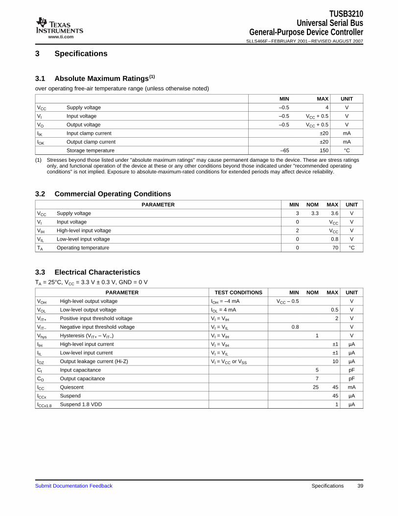
3.1 Absolute Maximum Ratings (1)
3.2 Commercial Operating Conditions
3.3 Electrical Characteristics
TUSB3210Universal Serial Bus
General-Purpose Device ControllerSLLS466F–FEBRUARY 2001–REVISED AUGUST 2007
over operating free-air temperature range (unless otherwise noted)
MIN MAX UNIT
VCC Supply voltage –0.5 4 V
VI Input voltage –0.5 VCC + 0.5 V
VO Output voltage –0.5 VCC + 0.5 V
IIK Input clamp current ±20 mA
IOK Output clamp current ±20 mA
Storage temperature –65 150 °C
(1) Stresses beyond those listed under "absolute maximum ratings" may cause permanent damage to the device. These are stress ratingsonly, and functional operation of the device at these or any other conditions beyond those indicated under "recommended operatingconditions" is not implied. Exposure to absolute-maximum-rated conditions for extended periods may affect device reliability.
PARAMETER MIN NOM MAX UNIT
VCC Supply voltage 3 3.3 3.6 V
VI Input voltage 0 VCC V
VIH High-level input voltage 2 VCC V
VIL Low-level input voltage 0 0.8 V
TA Operating temperature 0 70 °C
TA = 25°C, VCC = 3.3 V ± 0.3 V, GND = 0 V
PARAMETER TEST CONDITIONS MIN NOM MAX UNIT
VOH High-level output voltage IOH = –4 mA VCC – 0.5 V
VOL Low-level output voltage IOL = 4 mA 0.5 V
VIT+ Positive input threshold voltage VI = VIH 2 V
VIT– Negative input threshold voltage VI = VIL 0.8 V
Vhys Hysteresis (VIT+ – VIT–) VI = VIH 1 V
IIH High-level input current VI = VIH ±1 μA
IIL Low-level input current VI = VIL ±1 μA
IOZ Output leakage current (Hi-Z) VI = VCC or VSS 10 μA
CI Input capacitance 5 pF
CO Output capacitance 7 pF
ICC Quiescent 25 45 mA
ICCx Suspend 45 μA
ICCx1.8 Suspend 1.8 VDD 1 μA
Submit Documentation Feedback Specifications 39
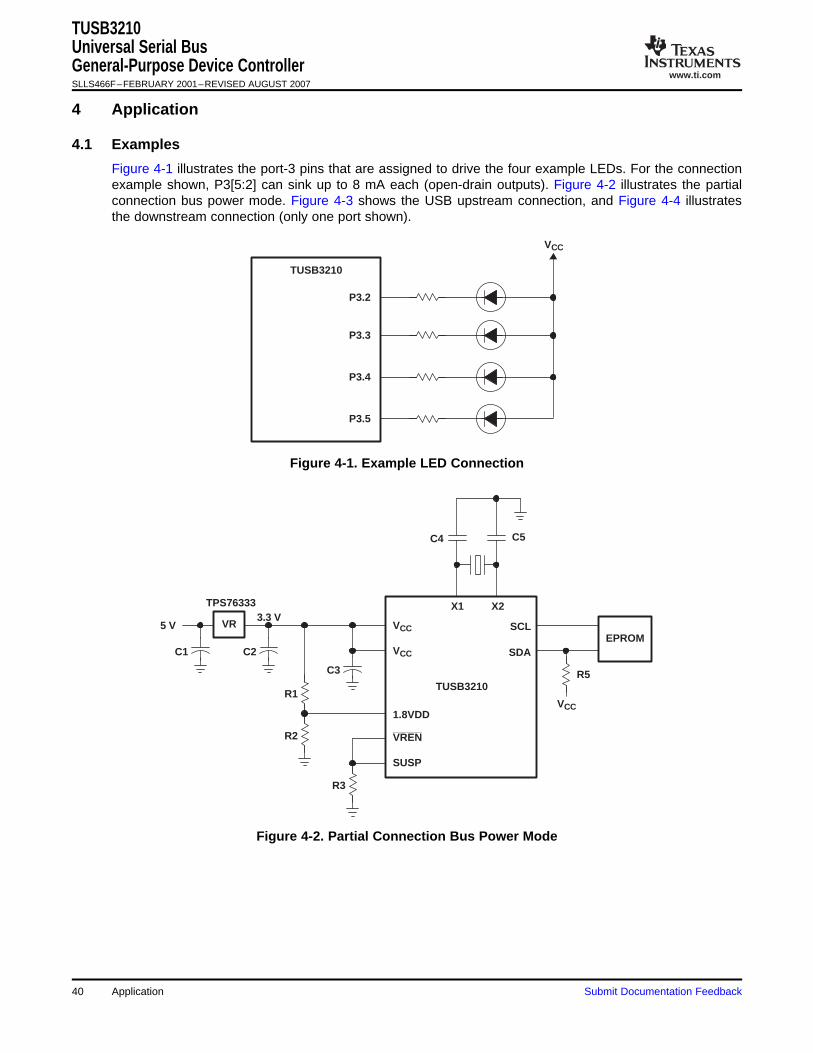
www.ti.com
4 Application
4.1 Examples
TUSB3210
P3.2
P3.3
P3.4
P3.5
VCC
C3
R1
R2
R3
R5
VCC
EPROMVCC
VCC
1.8VDD
VREN
SUSP
C4 C5
X1 X2
SCL
SDA
TUSB3210
C2
VR
TPS76333
C1
5 V3.3 V
TUSB3210Universal Serial BusGeneral-Purpose Device ControllerSLLS466F–FEBRUARY 2001–REVISED AUGUST 2007
Figure 4-1 illustrates the port-3 pins that are assigned to drive the four example LEDs. For the connectionexample shown, P3[5:2] can sink up to 8 mA each (open-drain outputs). Figure 4-2 illustrates the partialconnection bus power mode. Figure 4-3 shows the USB upstream connection, and Figure 4-4 illustratesthe downstream connection (only one port shown).
Figure 4-1. Example LED Connection
Figure 4-2. Partial Connection Bus Power Mode
Application40 Submit Documentation Feedback
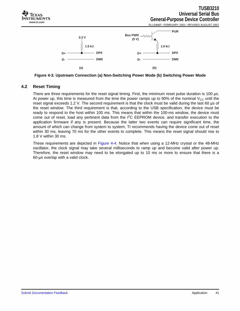
www.ti.com
3.3 V
1.5 kΩ
D+
D-
DP0
DM0
1.5 kΩ
D+
D-
DP0
DM0
Bus PWR(5 V)
PUR
(a) (b)
4.2 Reset Timing
TUSB3210Universal Serial Bus
General-Purpose Device ControllerSLLS466F–FEBRUARY 2001–REVISED AUGUST 2007
Figure 4-3. Upstream Connection (a) Non-Switching Power Mode (b) Switching Power Mode
There are three requirements for the reset signal timing. First, the minimum reset pulse duration is 100 μs.At power up, this time is measured from the time the power ramps up to 90% of the nominal VCC until thereset signal exceeds 1.2 V. The second requirement is that the clock must be valid during the last 60 μs ofthe reset window. The third requirement is that, according to the USB specification, the device must beready to respond to the host within 100 ms. This means that within the 100-ms window, the device mustcome out of reset, load any pertinent data from the I2C EEPROM device, and transfer execution to theapplication firmware if any is present. Because the latter two events can require significant time, theamount of which can change from system to system, TI recommends having the device come out of resetwithin 30 ms, leaving 70 ms for the other events to complete. This means the reset signal should rise to1.8 V within 30 ms.
These requirements are depicted in Figure 4-4. Notice that when using a 12-MHz crystal or the 48-MHzoscillator, the clock signal may take several milliseconds to ramp up and become valid after power up.Therefore, the reset window may need to be elongated up to 10 ms or more to ensure that there is a60-μs overlap with a valid clock.
Submit Documentation Feedback Application 41
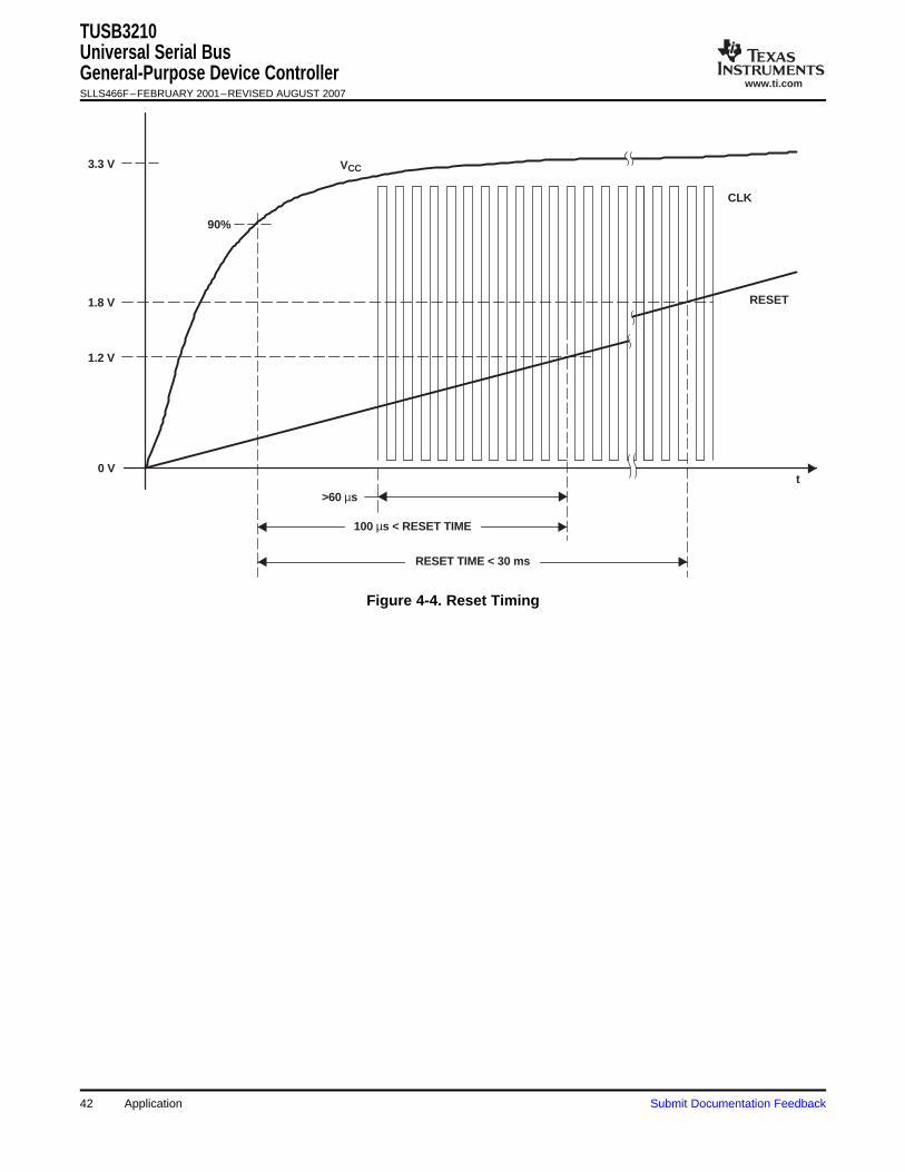
www.ti.com
CLK
RESET
t
VCC
90%
3.3 V
1.2 V
0 V
>60 µs
100 µs < RESET TIME
1.8 V
RESET TIME < 30 ms
TUSB3210Universal Serial BusGeneral-Purpose Device ControllerSLLS466F–FEBRUARY 2001–REVISED AUGUST 2007
Figure 4-4. Reset Timing
Application42 Submit Documentation Feedback
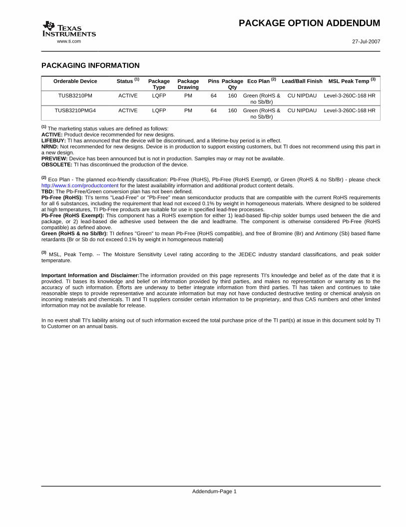
PACKAGING INFORMATION
Orderable Device Status (1) PackageType
PackageDrawing
Pins PackageQty
Eco Plan (2) Lead/Ball Finish MSL Peak Temp (3)
TUSB3210PM ACTIVE LQFP PM 64 160 Green (RoHS &no Sb/Br)
CU NIPDAU Level-3-260C-168 HR
TUSB3210PMG4 ACTIVE LQFP PM 64 160 Green (RoHS &no Sb/Br)
CU NIPDAU Level-3-260C-168 HR
(1) The marketing status values are defined as follows:ACTIVE: Product device recommended for new designs.LIFEBUY: TI has announced that the device will be discontinued, and a lifetime-buy period is in effect.NRND: Not recommended for new designs. Device is in production to support existing customers, but TI does not recommend using this part ina new design.PREVIEW: Device has been announced but is not in production. Samples may or may not be available.OBSOLETE: TI has discontinued the production of the device.
(2) Eco Plan - The planned eco-friendly classification: Pb-Free (RoHS), Pb-Free (RoHS Exempt), or Green (RoHS & no Sb/Br) - please checkhttp://www.ti.com/productcontent for the latest availability information and additional product content details.TBD: The Pb-Free/Green conversion plan has not been defined.Pb-Free (RoHS): TI's terms "Lead-Free" or "Pb-Free" mean semiconductor products that are compatible with the current RoHS requirementsfor all 6 substances, including the requirement that lead not exceed 0.1% by weight in homogeneous materials. Where designed to be solderedat high temperatures, TI Pb-Free products are suitable for use in specified lead-free processes.Pb-Free (RoHS Exempt): This component has a RoHS exemption for either 1) lead-based flip-chip solder bumps used between the die andpackage, or 2) lead-based die adhesive used between the die and leadframe. The component is otherwise considered Pb-Free (RoHScompatible) as defined above.Green (RoHS & no Sb/Br): TI defines "Green" to mean Pb-Free (RoHS compatible), and free of Bromine (Br) and Antimony (Sb) based flameretardants (Br or Sb do not exceed 0.1% by weight in homogeneous material)
(3) MSL, Peak Temp. -- The Moisture Sensitivity Level rating according to the JEDEC industry standard classifications, and peak soldertemperature.
Important Information and Disclaimer:The information provided on this page represents TI's knowledge and belief as of the date that it isprovided. TI bases its knowledge and belief on information provided by third parties, and makes no representation or warranty as to theaccuracy of such information. Efforts are underway to better integrate information from third parties. TI has taken and continues to takereasonable steps to provide representative and accurate information but may not have conducted destructive testing or chemical analysis onincoming materials and chemicals. TI and TI suppliers consider certain information to be proprietary, and thus CAS numbers and other limitedinformation may not be available for release.
In no event shall TI's liability arising out of such information exceed the total purchase price of the TI part(s) at issue in this document sold by TIto Customer on an annual basis.
PACKAGE OPTION ADDENDUM
www.ti.com 27-Jul-2007
Addendum-Page 1
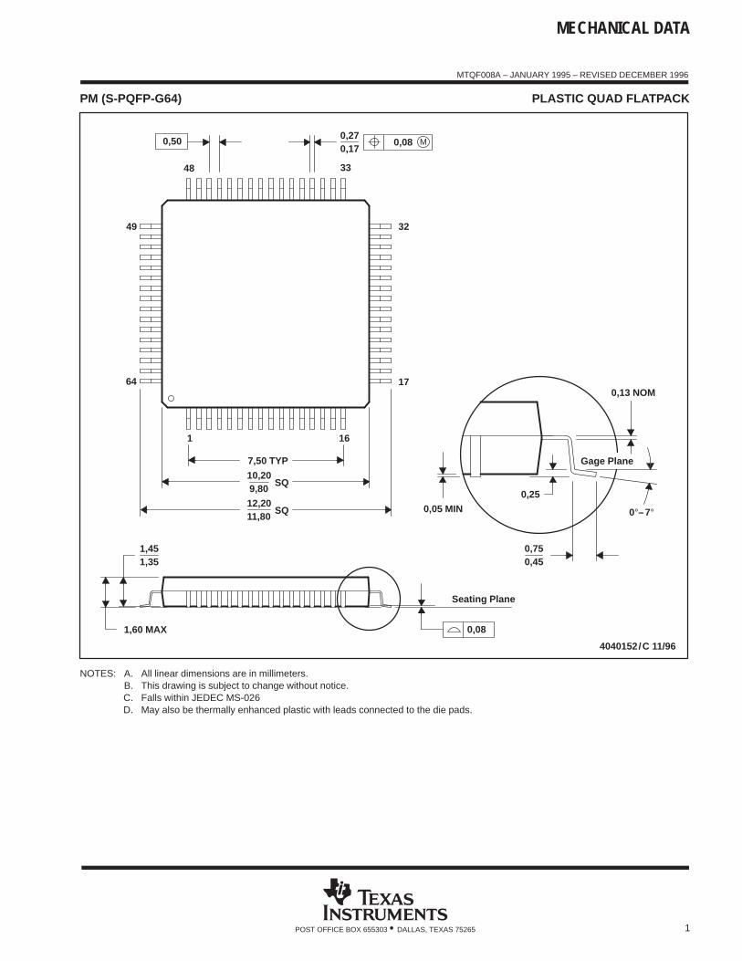
MECHANICAL DATA
MTQF008A – JANUARY 1995 – REVISED DECEMBER 1996
1POST OFFICE BOX 655303 • DALLAS, TEXAS 75265
PM (S-PQFP-G64) PLASTIC QUAD FLATPACK
4040152/C 11/96
32
170,13 NOM
0,25
0,450,75
Seating Plane
0,05 MIN
Gage Plane
0,27
33
16
48
1
0,17
49
64
SQ
SQ10,20
11,8012,20
9,80
7,50 TYP
1,60 MAX
1,451,35
0,08
0,50 M0,08
0°–7°
NOTES: A. All linear dimensions are in millimeters.B. This drawing is subject to change without notice.C. Falls within JEDEC MS-026D. May also be thermally enhanced plastic with leads connected to the die pads.
IMPORTANT NOTICE
Texas Instruments Incorporated and its subsidiaries (TI) reserve the right to make corrections, modifications, enhancements,improvements, and other changes to its products and services at any time and to discontinue any product or service without notice.Customers should obtain the latest relevant information before placing orders and should verify that such information is current andcomplete. All products are sold subject to TI’s terms and conditions of sale supplied at the time of order acknowledgment.
TI warrants performance of its hardware products to the specifications applicable at the time of sale in accordance with TI’sstandard warranty. Testing and other quality control techniques are used to the extent TI deems necessary to support thiswarranty. Except where mandated by government requirements, testing of all parameters of each product is not necessarilyperformed.
TI assumes no liability for applications assistance or customer product design. Customers are responsible for their products andapplications using TI components. To minimize the risks associated with customer products and applications, customers shouldprovide adequate design and operating safeguards.
TI does not warrant or represent that any license, either express or implied, is granted under any TI patent right, copyright, maskwork right, or other TI intellectual property right relating to any combination, machine, or process in which TI products or servicesare used. Information published by TI regarding third-party products or services does not constitute a license from TI to use suchproducts or services or a warranty or endorsement thereof. Use of such information may require a license from a third party underthe patents or other intellectual property of the third party, or a license from TI under the patents or other intellectual property of TI.
Reproduction of TI information in TI data books or data sheets is permissible only if reproduction is without alteration and isaccompanied by all associated warranties, conditions, limitations, and notices. Reproduction of this information with alteration is anunfair and deceptive business practice. TI is not responsible or liable for such altered documentation. Information of third partiesmay be subject to additional restrictions.
Resale of TI products or services with statements different from or beyond the parameters stated by TI for that product or servicevoids all express and any implied warranties for the associated TI product or service and is an unfair and deceptive businesspractice. TI is not responsible or liable for any such statements.
TI products are not authorized for use in safety-critical applications (such as life support) where a failure of the TI product wouldreasonably be expected to cause severe personal injury or death, unless officers of the parties have executed an agreementspecifically governing such use. Buyers represent that they have all necessary expertise in the safety and regulatory ramificationsof their applications, and acknowledge and agree that they are solely responsible for all legal, regulatory and safety-relatedrequirements concerning their products and any use of TI products in such safety-critical applications, notwithstanding anyapplications-related information or support that may be provided by TI. Further, Buyers must fully indemnify TI and itsrepresentatives against any damages arising out of the use of TI products in such safety-critical applications.
TI products are neither designed nor intended for use in military/aerospace applications or environments unless the TI products arespecifically designated by TI as military-grade or "enhanced plastic." Only products designated by TI as military-grade meet militaryspecifications. Buyers acknowledge and agree that any such use of TI products which TI has not designated as military-grade issolely at the Buyer's risk, and that they are solely responsible for compliance with all legal and regulatory requirements inconnection with such use.
TI products are neither designed nor intended for use in automotive applications or environments unless the specific TI productsare designated by TI as compliant with ISO/TS 16949 requirements. Buyers acknowledge and agree that, if they use anynon-designated products in automotive applications, TI will not be responsible for any failure to meet such requirements.
Following are URLs where you can obtain information on other Texas Instruments products and application solutions:
Products Applications
Amplifiers amplifier.ti.com Audio www.ti.com/audio
Data Converters dataconverter.ti.com Automotive www.ti.com/automotive
DSP dsp.ti.com Broadband www.ti.com/broadband
Interface interface.ti.com Digital Control www.ti.com/digitalcontrol
Logic logic.ti.com Military www.ti.com/military
Power Mgmt power.ti.com Optical Networking www.ti.com/opticalnetwork
Microcontrollers microcontroller.ti.com Security www.ti.com/security
RFID www.ti-rfid.com Telephony www.ti.com/telephony
Low Power www.ti.com/lpw Video & Imaging www.ti.com/videoWireless
Wireless www.ti.com/wireless
Mailing Address: Texas Instruments, Post Office Box 655303, Dallas, Texas 75265Copyright © 2007, Texas Instruments Incorporated