Embed Size (px)
Citation preview
1
Unit 2
Circuit Design Process
In this chapter we will be studying how to get the schematic into stick diagrams or
layouts. MOS circuits are formed on four basic layers:
� N-diffusion
� P-diffusion
� Polysilicon
� Metal
These layers are isolated by one another by thick or thin silicon dioxide insulating
layers.
Thin oxide mask region includes n-diffusion / p-diffusion and transistor channel.
Stick diagrams:
Stick diagrams may be used to convey layer information through the use of a color code.
For example: n-diffusion --green
poly -- red
blue -- metal
yellow --implant
black --contact areas
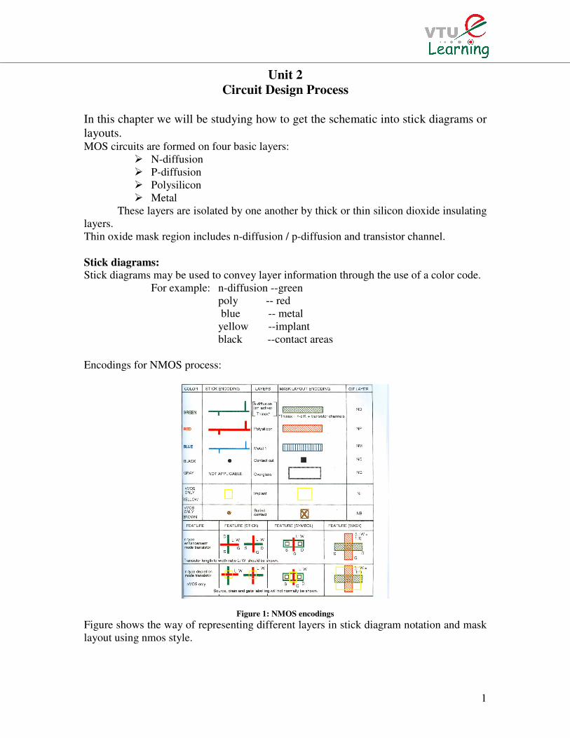
Encodings for NMOS process:
Figure 1: NMOS encodings
Figure shows the way of representing different layers in stick diagram notation and mask
layout using nmos style.
2
Figure1 shows when a n-transistor is formed: a transistor is formed when a green line (n+
diffusion) crosses a red line (poly) completely. Figure also shows how a depletion mode
transistor is represented in the stick format.
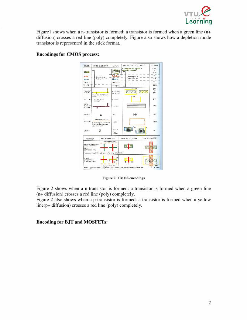
Encodings for CMOS process:
Figure 2: CMOS encodings
Figure 2 shows when a n-transistor is formed: a transistor is formed when a green line
(n+ diffusion) crosses a red line (poly) completely.
Figure 2 also shows when a p-transistor is formed: a transistor is formed when a yellow
line(p+ diffusion) crosses a red line (poly) completely.
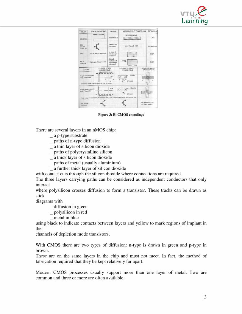
Encoding for BJT and MOSFETs:
3
Figure 3: Bi CMOS encodings
There are several layers in an nMOS chip:
_ a p-type substrate
_ paths of n-type diffusion
_ a thin layer of silicon dioxide
_ paths of polycrystalline silicon
_ a thick layer of silicon dioxide
_ paths of metal (usually aluminium)
_ a further thick layer of silicon dioxide
with contact cuts through the silicon dioxide where connections are required.
The three layers carrying paths can be considered as independent conductors that only
interact
where polysilicon crosses diffusion to form a transistor. These tracks can be drawn as
stick
diagrams with
_ diffusion in green
_ polysilicon in red
_ metal in blue
using black to indicate contacts between layers and yellow to mark regions of implant in
the
channels of depletion mode transistors.
With CMOS there are two types of diffusion: n-type is drawn in green and p-type in
brown.
These are on the same layers in the chip and must not meet. In fact, the method of
fabrication required that they be kept relatively far apart.
Modern CMOS processes usually support more than one layer of metal. Two are
common and three or more are often available.
4
Actually, these conventions for colors are not universal; in particular, industrial (rather
than academic) systems tend to use red for diffusion and green for polysilicon. Moreover,
a shortage of colored pens normally means that both types of diffusion in CMOS are
colored green and the polarity indicated by drawing a circle round p-type transistors or
simply inferred from the context. Colorings for multiple layers of metal are even less
standard.
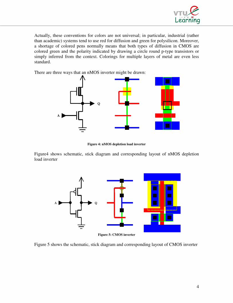
There are three ways that an nMOS inverter might be drawn:
Figure 4: nMOS depletion load inverter
Figure4 shows schematic, stick diagram and corresponding layout of nMOS depletion
load inverter
Figure 5: CMOS inverter
Figure 5 shows the schematic, stick diagram and corresponding layout of CMOS inverter
5
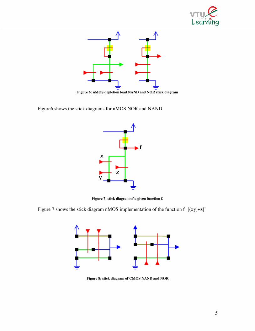
Figure 6: nMOS depletion load NAND and NOR stick diagram
Figure6 shows the stick diagrams for nMOS NOR and NAND.
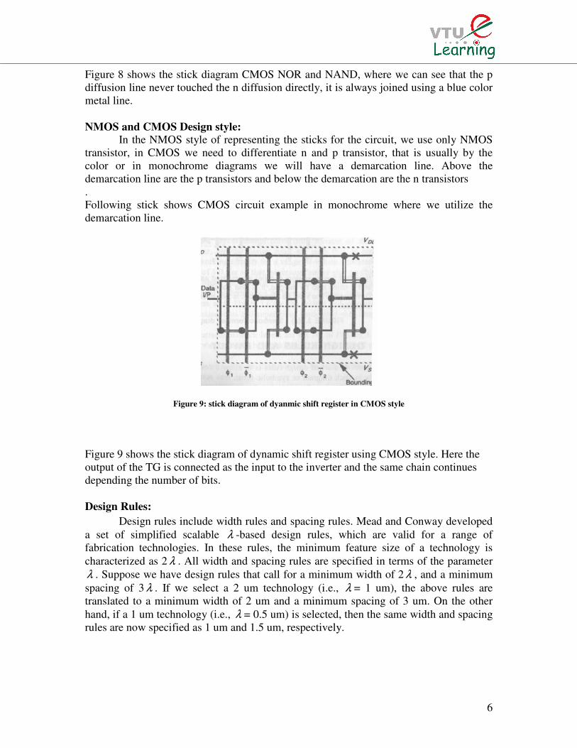
Figure 7: stick diagram of a given function f.
Figure 7 shows the stick diagram nMOS implementation of the function f=[(xy)+z]’
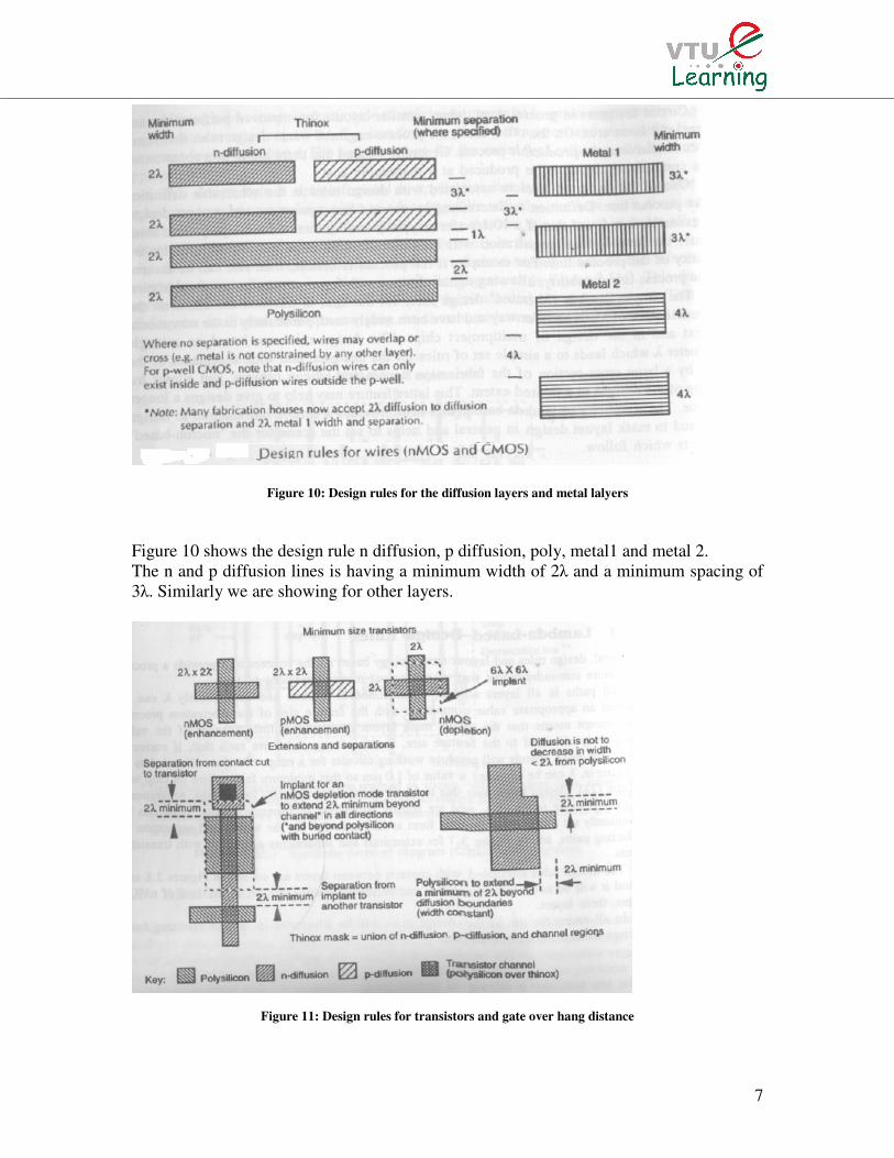
Figure 8: stick diagram of CMOS NAND and NOR
6
Figure 8 shows the stick diagram CMOS NOR and NAND, where we can see that the p
diffusion line never touched the n diffusion directly, it is always joined using a blue color
metal line.
NMOS and CMOS Design style:
In the NMOS style of representing the sticks for the circuit, we use only NMOS
transistor, in CMOS we need to differentiate n and p transistor, that is usually by the
color or in monochrome diagrams we will have a demarcation line. Above the
demarcation line are the p transistors and below the demarcation are the n transistors
.
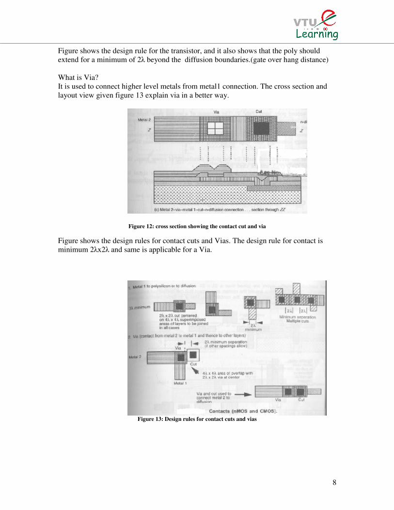
Following stick shows CMOS circuit example in monochrome where we utilize the
demarcation line.
Figure 9: stick diagram of dyanmic shift register in CMOS style
Figure 9 shows the stick diagram of dynamic shift register using CMOS style. Here the
output of the TG is connected as the input to the inverter and the same chain continues
depending the number of bits.
Design Rules:
Design rules include width rules and spacing rules. Mead and Conway developed
a set of simplified scalable λ -based design rules, which are valid for a range of
fabrication technologies. In these rules, the minimum feature size of a technology is
characterized as 2 λ . All width and spacing rules are specified in terms of the parameter
λ . Suppose we have design rules that call for a minimum width of 2 λ , and a minimum
spacing of 3 λ . If we select a 2 um technology (i.e., λ = 1 um), the above rules are
translated to a minimum width of 2 um and a minimum spacing of 3 um. On the other
hand, if a 1 um technology (i.e., λ = 0.5 um) is selected, then the same width and spacing
rules are now specified as 1 um and 1.5 um, respectively.
7
Figure 10: Design rules for the diffusion layers and metal lalyers
Figure 10 shows the design rule n diffusion, p diffusion, poly, metal1 and metal 2.
The n and p diffusion lines is having a minimum width of 2λ and a minimum spacing of
3λ. Similarly we are showing for other layers.
Figure 11: Design rules for transistors and gate over hang distance
8
Figure shows the design rule for the transistor, and it also shows that the poly should
extend for a minimum of 2λ beyond the diffusion boundaries.(gate over hang distance)
What is Via?
It is used to connect higher level metals from metal1 connection. The cross section and
layout view given figure 13 explain via in a better way.
Figure 12: cross section showing the contact cut and via
Figure shows the design rules for contact cuts and Vias. The design rule for contact is
minimum 2λx2λ and same is applicable for a Via.
Figure 13: Design rules for contact cuts and vias
9
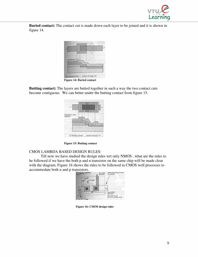
Buried contact: The contact cut is made down each layer to be joined and it is shown in
figure 14.
Figure 14: Buried contact
Butting contact: The layers are butted together in such a way the two contact cuts
become contiguous. We can better under the butting contact from figure 15.
Figure 15: Butting contact
CMOS LAMBDA BASED DESIGN RULES:
Till now we have studied the design rules wrt only NMOS , what are the rules to
be followed if we have the both p and n transistor on the same chip will be made clear
with the diagram. Figure 16 shows the rules to be followed in CMOS well processes to
accommodate both n and p transistors.
Figure 16: CMOS design rules
10
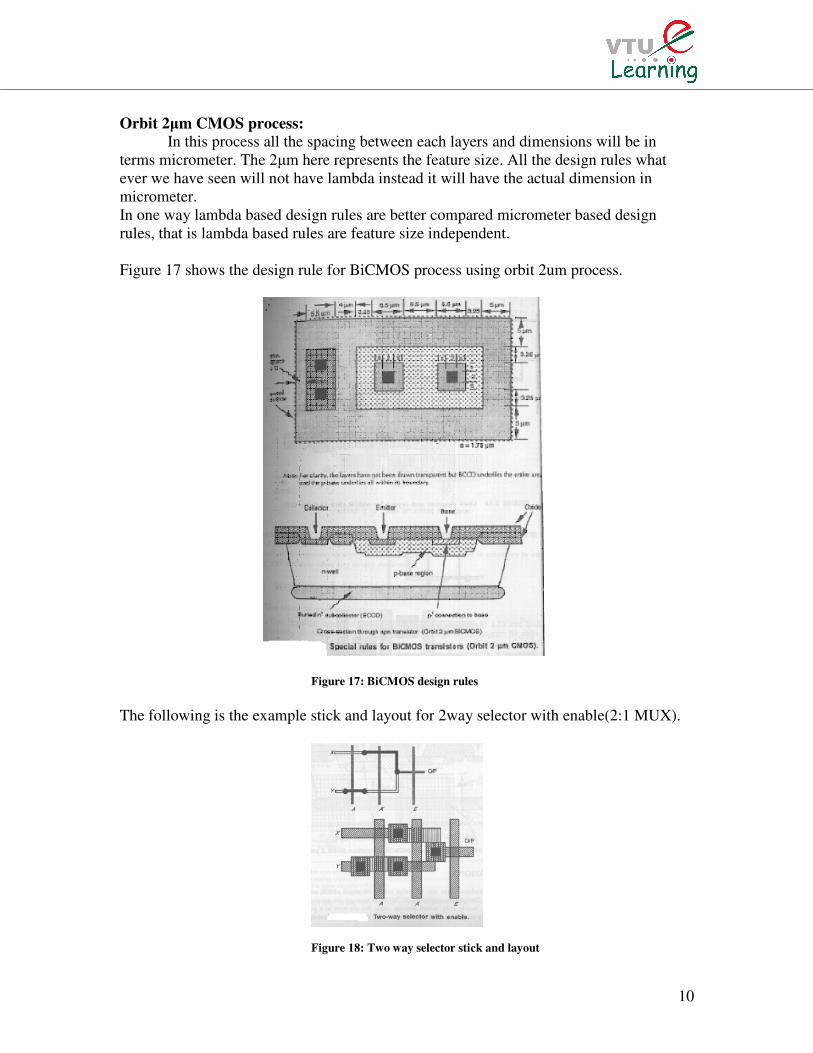
Orbit 2µm CMOS process:
In this process all the spacing between each layers and dimensions will be in
terms micrometer. The 2µm here represents the feature size. All the design rules what
ever we have seen will not have lambda instead it will have the actual dimension in
micrometer.
In one way lambda based design rules are better compared micrometer based design
rules, that is lambda based rules are feature size independent.
Figure 17 shows the design rule for BiCMOS process using orbit 2um process.
Figure 17: BiCMOS design rules
The following is the example stick and layout for 2way selector with enable(2:1 MUX).
Figure 18: Two way selector stick and layout

11