Embed Size (px)
Citation preview

UNIQUE FEATURES OF A 40/20 METER HOMEBREW RECEIVERLEE SNOOK W1DN
HIGHWAY 285 TECHCONNECT CLUB
TECHFEST
NOVEMBER 3, 2018

PROJECT GOALS
• Simple receiver design with readily available parts
• Adequate specifications for general use
• At home fabrication techniques
• Simple reconfiguration for the Arduino Controller and LCD Display Layout
• 50 ohm Interstage coupling for easy testing of each stage
2

WILL FOCUS ON THE FOLLOWING TOPICS
• History
• Block Diagram and Overview
• General Specifications
• LO Frequency Selection
• I.F. Crystal Filter Design
• Microprocessor Controlled (ATMEGA 328)
• Arduino Based Development System
• 7 inch Color LCD Touch Display
• 4D Systems IDE for display configuration
• At home PCB fabrication
• Single Sided PCB, Maximize Ground Plane
• Rotarty Encoder Tuning Knob with selectable increments
• Variable Lowpass Audio Filter
• Two Local Oscillator DDS synthesizers
• Solid state front end switching
• Band Spectrum Display
• 10 User Memories
• Simulated Analog S Meter
• Externally programmable through a serial port
• 50 ohm Interstage coupling impedance
• Passband Offset Tuning
3

HISTORY
• First Receiver – Foxhole Radio
• Razor Blade as a crystal detector
• Of course, 110 turns on a toilet paper
roll
• Second Receiver – Dual Slide Tuning
• 5th Grade
• 11 years old
4

HISTORYMY FIRST MODULAR
RECEIVER BREADBOARD.
EACH MODULE IS ON
IT’S OWN PCB WITH 50
OHMS IN AND OUT
5

HISTORYSECOND RECEIVER USING INDIVIDUAL PLUG IN MODULES AND A LCD DISPLAY
6

7

HISTORY ITERATION WITH 4D SYSTEMS COLOR TOUCH 4 INCH DISPLAY
8

HISTORYFOURTH RECEIVER(TODAY)
9

10
Internal view

BLOCK
DIAGRAM
11

LAYOUT
12

GENERAL SPECIFICATIONS
•Sensitivity -120 dBm BW = 3200 Hz
• IMD -42 dBm
•Third Order Intercept ((120-42)/2+42 = -3 dBm
•SFDR 120-42 = 92 dbm
13

LOCAL AND PRODUCT DETECTOR FREQUENCY SELECTION TABLE
Select a Local oscillator (LO) such that:
(use the lower cutoff edge since it has the steepest shape factor)
• As the receive frequency increase, the LO increases
• For LSB and USB the sideband falls within the crystal filter passband
14
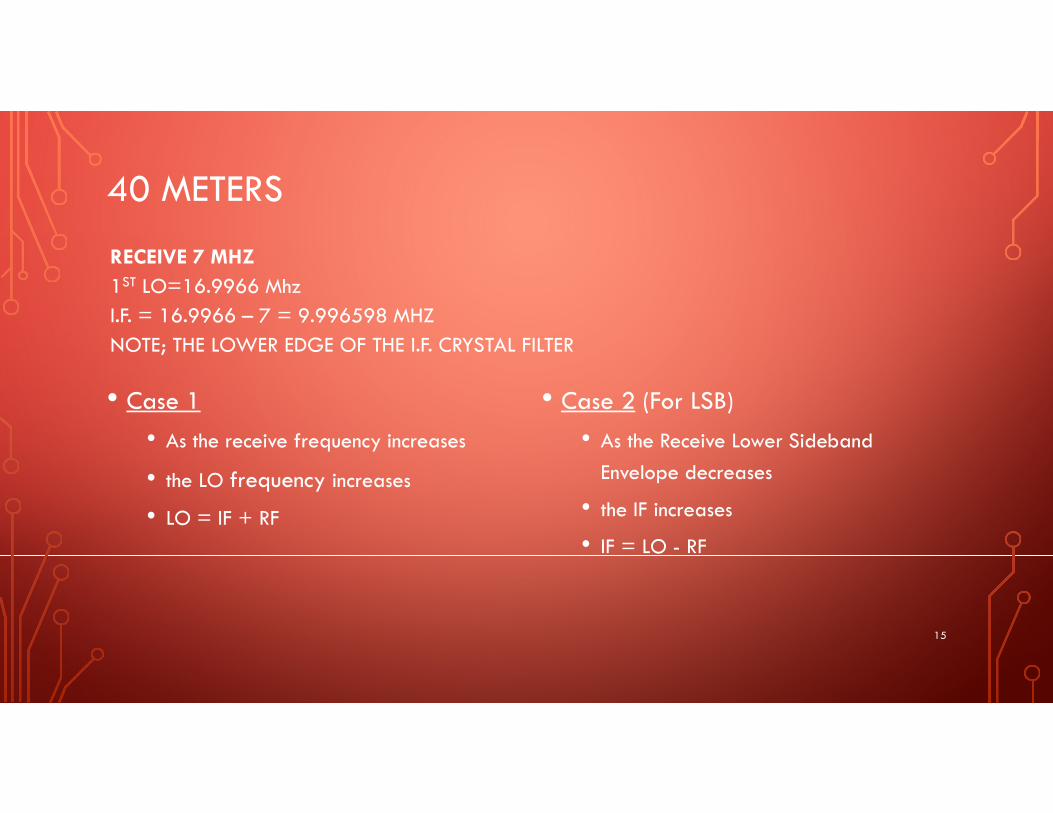
40 METERS
RECEIVE 7 MHZ
1ST LO=16.9966 Mhz
I.F. = 16.9966 – 7 = 9.996598 MHZ
NOTE; THE LOWER EDGE OF THE I.F. CRYSTAL FILTER
• Case 1
• As the receive frequency increases
• the LO frequency increases
• LO = IF + RF
• Case 2 (For LSB)
• As the Receive Lower Sideband
Envelope decreases
• the IF increases
• IF = LO - RF
15

20 METERS
RECEIVE 14 MHZ
1ST LO=4.003402 Mhz
IF = RF - LO
• Case 1
• As the receive frequency increases
• the LO frequency increases
• LO = IF + RF
• Case 2 (For LSB)
• the Receive Lower Sideband Envelope
decreases
• the IF increases
• IF = LO - RF
16

EXAMPLES (CONT.)
RECEIVE 14 MHZ
1ST LO=4.003402 MHZ
I.F. = 14-4.003402= 9.996598 MHZ
NOTE; THE LOWER EDGE OF THE I.F. CRYSTAL FILTER
• Case 1; As the receive frequency increase, the
LO frequency increases
• Receive 14.1 Mhz
• 1st LO=4.003402 Mhz
• I.F. = 14.1 – 4.003402 = 10.096598 Mhz
Note; The Lower Edge of the I.F. Crystal Filter
• Case 2; For LSB, the Receive Lower Sideband
Envelope decreases, the IF increases
• Receive 6.999 Mhz, 1 khz audio tone
• 1st LO=16.9966 Mhz
• I.F. = 16.9966 – 6.999 = 9.9976 Mhz
Note; The LSB envelope is within the passband
17

CRYSTAL FILTER DESIGNMEASURE A GROUP OF 10 MHZ CRYSTALS AND SELECT 6 THAT HAVE THE CLOSEST PARAMETERS
18

CRYSTAL FILTER DESIGN (CONT.)
• For a review of Crystal Filter Design use the following reference
Crystal Motional Parameters, A Comparison of Measurement
Approaches
Jack R. Smith K8ZOA, 11 June 2006
• Using the Freeware Progam; DISHAL vers 2.0.5.2;
Enter Lm, Cm, Cp, BW, # of Xtals, Ripple
19

20

MEASURED RESULTBANDWITH FOR THIS FILTER = 3 kHz
21

MICROPROCESSOR (ATMEGA 328)
• The Arduino Uno prototyping board
• Arduino Uno is a microcontroller board based on the ATmega328PIt has 14 digital
input/output pins (of which 6 can be used as PWM outputs), 6 analog inputs, a 16 MHz
quartz crystal, a USB connection, a power jack, an ICSP header and a reset button. It contains
everything needed to support the microcontroller; simply connect it to a computer with a USB
cable or power it with a AC-to-DC adapter or battery to get started.
• Off-Boarding the ATMEG328 requires changing the pin assignments
• For instance; Programming a command to Pin 13 on the Uno Prototype board must now be
changed to Pin19 for the stand alone ATMEGA328. See the diagame below.
22

23

MICROPROCESSOR PROGRAMMING
• Programming either the Uno board or the stand alone processor
requires connecting a serial USB cable to the Uno USB port or, for
the stand alone case, using a MAX232 chip to convert the RS232
voltages to 5 volts.
• I use an USB to RS232 converter cable which can be purchased
online at;
https://www.amazon.com/Serial-RS232-Converter-Laptop-
Notebook/dp/B00404P0L624

MICROPROCESSOR PROGRAMMING (CONT.)
• A simple programming example:
• Make an LED blink. Connect and LED to Pin 13 of the Arduino Uno Proto board with
the appropriate series dropping resistor of 330 ohms.
• Note: The maximum current sourcing pin current is = 40 ma.
• An integrated development environment (IDE) is a software application that ides
comprehensive facilities to computer programmers for software development.
• Download the Arduino IDE at https://www.arduino.cc/en/Main/Software
25

Code;
// The setup function runs when you press reset or power the board
//Code in the setup(), Intitalizes Pins as Input or Output.
//Setup only runs Once on startup
// The void keyword is used only in function declarations. It indicates that the function is expected to return
no information
to the function from which it was called.
//The following code is for the UNO proto board, Pin 13 would be changed to pin 19 for the off boarded
processor.
void setup()
{
pinMode(Pin 13, OUTPUT); // initialize digital pin 13 as an output.
}
void loop() // The loop function runs over and over again forever
{
digitalWrite(Pin 13, HIGH); // turn the LED on (HIGH is the voltage level)
delay(500); // wait for a second
digitalWrite(Pin 13, LOW); // turn the LED off by making the voltage LOW
delay(500); // wait for a second
} 26
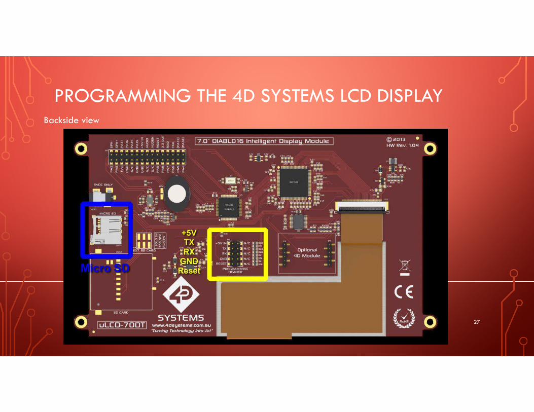
PROGRAMMING THE 4D SYSTEMS LCD DISPLAY
27
Backside view

PROGRAMMING THE LCD DISPLAY (CONT.)
• The microUSB Programming Adaptor
(uUSB-PA5 and uUSB-PA5-II) is a USB to
Serial-TTL UART bridge converter
• Insert the micro SD card into the PC USB
port (use micro to mini USB adapter
card if necessary)
• Connect uUSB-PA5 from +5V, TX, RX,
GND, Reset connector to PC USB port.
28

PROGRAMMING THE LCD DISPLAY
29
Boot up the IDE program

PROGRAMMING THE LCD DISPLAY (CONT.)
30
Select the ViSiGenie Display Type and Orientation

PROGRAMMING THE LCD DISPLAY (CONT.)
31
Select Progamming
Environment;
By simply laying the display
out with the wanted objects
and setting the events to
drive them, the code is
written automatically. ViSi-
Genie provides the latest
rapid development
experience from 4D Labs
PROGRAMMING THE LCD DISPLAY (CONT.)
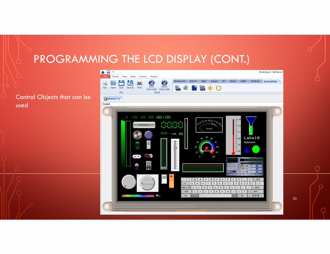
32
Control Objects that can be
used

PROGRAMMING THE LCD DISPLAY (CONT.)
33
Start the LCD layout by selecting and placing the “Objects” onto the
workspace.Example: In this example we will
place a Button on the screen and note the Object Inspector
Remember to Select the Comms Tab and Comm Port, it will turn Blue
when connected.Name and Index number.

PROGRAMMING THE LCD DISPLAY (CONT.)
34
Under Object Inspector on the right side of the screen, select the Events Tab and select “Report Message”.

EVENT HANDLER EXAMPLE
Void Setup(){Serial.begin(115200);genie.Begin(Serial);genie.AttachEventHandler(myGenieEventHandler);delay (2000); //let the display start upgenie.WriteContrast(brightness);}
35
The Arduino Code (in the Event Handler) will look for a Winbutton Event with an Index
of 0 and execute the user code when this button is pressed.
The programming language used for Arduino is based on C language. The syntax is almost identical to that of C or C++.

EVENT HANDLER EXAMPLE (CONT.)
Void Loop(){
genie.DoEvents();}
//-----------------------------------------Event Handler-------------------------------------------------------void myGenieEventHandler(void)
{genieFrame Event;
genie.DequeueEvent(&Event);
if(Event.reportObject.cmd == GENIE_REPORT_EVENT)
{
if (Event.reportObject.object == GENIE_OBJ_WINBUTTON)
{
//------------------------If Winbutton Pressed, Do Something-----------------------------------if (Event.reportObject.index == 0) // If Button(0)
{//Do Something
}36

PCB FABRICATION PROCESS
37
I use PCB Artist for Schematic Capture and Board Layout
The Receiver Layout in PCB Artist:

PCB FABRICATION PROCESS (CONT.)
38
• Using an Ink Jet printer,
• print the Top Copper
side of the Layout
• High Contrast Black
• onto rough side of
transparent film
• Remember, under printer
settings, Flip the print under
the printer setup so that the
rough side is facing the
photo sensitive side of the
PCD board.

PCB FABRICATION PROCESS (CONT.)
39
• Remove the light
protective film from
the photo sensitive
PCB board
• Insert the photo
sensitive board under
the transparent film
and expose in a
lightbox
PCB FABRICATION PROCESS (CONT.)
• Heat Developer and Ferric Chloride to ∼90 degrees F.
• Exposed PCB into glass tray with PCB Developer
• DATAK Cat. No 12-404 Positive Type PCB Developer
• Developer concentrate diluted 1:10 with water.
•Agitate until the Light Sensitive Film (Green color) is dissolved
between traces.
•Wash the board
40

PCB FABRICATION PROCESS (CONT.)
• Board into Ferric Chloride Etchant Solution bath
• MG Chemicals #415-1L,945 ml bottles Ferric Chloride
• Typically 15 minutes
• Periodically agitate
• Inspect and remove when the copper between traces has been
dissolved
•Wash off Ferric Chloride with fresh water
41

PCB FABRICATION PROCESS (CONT.)
42

QUADRATURE ROTARY ENCODERSPARKFUN ELECTRONICS; PN COM-11102
43

QUADRATURE ROTARY ENCODER (CONT.)
44
An RC time network was added to Ports A and B for Debounce. R=10k and C=.01µf.

45
In the following code;
A1=Sample 1 of Port A
A2=Sample 2 of Port A
B=Sample Port B
//------------------------Rotarty Encoder------------------------
A1=digitalRead(Encoder_Pin1);
delay(15); //Delay next sample by
15 ms
A2=digitalRead (Encoder_Pin1);
B=digitalRead(Encoder_Pin2);
Quadrature Rotary Encoder (cont.)

46
if (A1>A2) //A1(sample 1) is greater
than A2(sample 2)
{
if (B==HIGH)
{
f_rx=f_rx+increment[inc_pointer]; //Increase frequency
by increment
freq_low=(f_rx%10000);
freq_high=(f_rx-freq_low)/10000;
genie.WriteObject(GENIE_OBJ_LED_DIGITS, 2, freq_low);
genie.WriteObject(GENIE_OBJ_LED_DIGITS, 3, freq_high);
load1();
}
else //A(sample 1) is less than
A(sample 2)
{
f_rx=f_rx-increment[inc_pointer]; //Decrease frequency
by increment
freq_low=(f_rx%10000);
freq_high=(f_rx-freq_low)/10000;
genie.WriteObject(GENIE_OBJ_LED_DIGITS, 2, freq_low);
genie.WriteObject(GENIE_OBJ_LED_DIGITS, 3, freq_high);
load1();
}
}
More work is required, sometimes the encoder will skip a count when turning the wheel too fast.
VARIABLE BANDPASS AUDIO FILTER
• MAX7403 is a 8th-order, lowpass, elliptic, switched-capacitor filters
• These devices draw 2mA of supply current and allow corner frequencies
from1Hz to 10kHz
• Two clocking options are available
• self-clocking through the use of an external capacitor
• external clocking for tighter cutoff-frequency control
• Cutoff Frequency=Clock/100. Fosc(kHz)=(38*10000)/Cosc; Cosc is in pf.
• For my application, I used external capacitors (self clocking) switched with a
solid state single pole three throw switch (TS5A3357)47

VARIABLE BANDPASS AUDIO FILTER (CONT.)
48

VARIABLE BANDPASS AUDIO FILTER (CONT.)
• Audio Lowpass
Filter Frequency
Response
49-25
-20
-15
-10
-5
0
5
0 500 1000 1500 2000 2500 3000 3500 4000
3000
2400
1800
700

DDS (DIRECT DIGITAL SYNTHESIZERS (AD9850)DDS TUTORIAL
• Traditional designs of high bandwidth frequency synthesizers employ the use
of a phase-locked-loop (PLL).
• A direct digital synthesizer (DDS) provides many significant advantages over
the PLL approaches
• Fast settling time
• Sub-Hertz frequency resolution
• Continuous-phase switching response
• Low phase noise
50

DIRECT DIGITAL SYNTHESIZERS (CONT.)
• A DDS produces a sine wave at a given frequency
• The frequency depends on two variables
• Reference-clock frequency
• Binary number programmed into the frequency register (tuning word)
51

DIRECT DIGITAL SYNTHESIZERS (CONT.)
• Binary number in frequency register provides main input to phase accumulator
• Sine look-up table used
• Phase accumulator computes phase (angle) address for look-up table
• Outputs the digital value of amplitude
• Crresponding to the sine of that phase angle—to DAC
• DAC converts number to a corresponding value of analog voltage or current
52

DIRECT DIGITAL SYNTHESIZERS (CONT.)
• To generate a fixed-frequency sine wave, constant value (the phase increment
– from binary number added to the phase accumulator with each clock cycle.
• If the phase increment is large, the phase accumulator will step quickly through the sine
look-up table and thus generate a high frequency sine wave.
• If the phase increment is small, the phase accumulator will take many more steps,
accordingly generating a slower waveform
53

DIRECT DIGITAL SYNTHESIZERS (CONT.)
• Consider the case for n = 32, and M = 1. The phase accumulator steps through each of 232 possible
outputs before it overflows and restarts. The corresponding output sinewave frequency is equal to the
input clock frequency divided by 2^32. If M=2, then the phase accumulator register "rolls over" twice as
fast, and the output frequency is doubled. This can be generalized as follows.
• For an n-bit phase accumulator (n generally ranges from 24 to 32 in most DDS systems), there are 2n
possible phase points. The digital word in the delta phase register, M, represents the amount the phase
accumulator is incremented each clock cycle. If fc is the clock frequency, then the frequency of the output
sinewave is equal to:
• fOUT = (Δ Phase × CLKIN)/232
• Δ Phase=( fOUT ×232)/ CLKIN
54

DIRECT DIGITAL SYNTHESIZERS
• AD9850 is a highly integrated
device that uses advanced DDS
technology coupled with an internal
high speed, high performance D/A
converter and comparator to form a
complete, digitally programmable
frequency synthesizer and clock
generator function.
• Premounted on a small PCB online
from either Amazon or Digikey.55
DIRECT DIGITAL SYNTHESIZER (AD9850)
• The frequency tuning, control, and phase modulation words are loaded into
the AD9850 via
• Parallel byte or
• Serial loading format (I used the serial loading format)
• In serial load mode, subsequent rising edges of W_CLK shift the 1-bit data on
Pin 25 (D7) through the 40 bits of programming information.
• After 40 bits are shifted through, an FQ_UD pulse is required to update the
output frequency (or phase).
56

57
The Arduino Code for loading the DDS synthesizer:
//--------------------DDS Loader------------------------------
long function_delta_phase1()
{
freq_dds1=f_rx+if_center-offset;
//From the equation above ∆ Phase=( fOUT ×232)/ CLKIN
long delta_phase1 =(((freq_dds1)*pow(2,32))/clock);
return (delta_phase1);
void load1()
{
long delta_phase1=function_delta_phase1();
digitalWrite (LOAD1_Pin, LOW);
shiftOut(DATA_Pin, CLOCK_Pin, LSBFIRST, delta_phase1);
shiftOut(DATA_Pin, CLOCK_Pin, LSBFIRST, delta_phase1 >>
8);
shiftOut(DATA_Pin, CLOCK_Pin, LSBFIRST, delta_phase1 >>
16);
shiftOut(DATA_Pin, CLOCK_Pin, LSBFIRST, delta_phase1 >>
24);
shiftOut(DATA_Pin, CLOCK_Pin, LSBFIRST, 0x0);
digitalWrite (LOAD1_Pin, HIGH);
}


![Data Arduino UNO [Unlocked by Www.freemypdf.com]](https://img.pdfslide.us/doc/110x75/55cf98ae550346d033990fba/data-arduino-uno-unlocked-by-wwwfreemypdfcom.jpg)