Embed Size (px)
Citation preview
Unified Three-terminal Switch Model
for Current Mode Controls
Yingyi Yan
Thesis submitted to the Faculty of the
Virginia Polytechnic Institute and State University
in partial fulfillment of the requirements for the degree of
Master of Science
in
Electrical Engineering
Fred C. Lee, Chair
Dushan Boroyevich
Paolo Mattavelli
November 8th, 2010
Blacksburg, Virginia
Keywords: current-mode control, modeling,
three-terminal switch model, equivalent circuit
© 2010, Yingyi Yan
Unified Three-terminal Switch Model
for Current Mode Controls
Yingyi Yan
(Abstract)
Current-mode control architectures with different implementation approaches have
been an indispensable technique in many applications, such as voltage regulator, power
factor correction, battery charger and LED driver. Since the inductor current ramp, one
of state variables influenced by the input voltage and the output voltage, is used in the
modulator in current-mode control without any low pass filter, high order harmonics play
important role in the feedback control. This is the reason for the difficulty in obtaining
the small-signal model for current-mode control in the frequency domain. A continuous
time domain model was recently proposed as a successful model for current-mode
control architectures with different implementation. However, the model was derived by
describing function method, which is very arithmatically complicated, not to mention
time consuming. Although an equivalent circuit for a current mode control Buck
converter was proposed to help designers to use the model without involving
complicated math, the equivalent circuit is not a complete model. Moreover, no
equivalent circuit for other topologies is available for designers. In this thesis, the
primary objective is to develop a unified three-terminal switch model for current-mode
control with different implementation methods, which are applicable in all the current
mode control power converters.
First, the existing model for current mode control is reviewed. The limitation of
average models and the discrete time model for current-mode control is identified. The
continuous time model and its equivalent circuit of Buck converter is introduced. The
deficiency of the equivalent circuit is discussed.
After that, a unified three-terminal switch model for current mode control is
presented. Based on the observation, the PWM switch and the closed current loop is
taken as an invariant sub-circuit which is common to different DC/DC converter
topologies. A basic small signal relationship between terminal currents is studied and the
result shows that the PWM switch with current feedback preserves the property of the
iii
PWM switch in power stage. A three-terminal equivalent circuit is developed to
represent the small signal behavior of this common sub-circuit. The proposed model is a
unified model, which is applicable in both constant frequency modulation and variable
frequency modulation. The physical meaning of the three-terminal equivalent circuit
model is discussed. The model is verified by SIMPLIS simulation in commonly used
converters for both constant frequency modulation and variable frequency modulation.
Then, based on the proposed unified model, a comparison between different
current mode control implementations is presented. In different applications, different
implementations have their unique benefit on extending control bandwidth. The
properties of audio susceptibility and output impedance are discussed. It is found that, for
adaptive voltage positioning design, constant on-time current mode control can
simplifies the outer loop design.
Next, since multiphase interleaving structure is widely used in PFC, voltage
regulator and other high current applications, the model is extended to multiphase current
mode control. Some design concerns are discussed based on the model.
As a conclusion, a unified three-terminal switch model for current mode controls is
investigated. The proposed model is quite general and not limited by implementation
methods and topologies. All the modeling results are verified through simulation and
experiments.

iv
Acknowledgments
For their support and direction over years, I would like to express my heartfelt
gratitude to all my professors at Virginia Tech, without whom my research and this
thesis would not have been possible. In particular, I am very grateful to my advisor
and committee chair, Professor Fred C. Lee, his kind help not only with research but
also with my life at Virginia Tech. He is always generous to give me suggestions and
ideas to help me focus on some unknown areas. His logical thoughts and earnest
attitude gave me courage when I met problems. He often shares his philosophy with me,
which is the most beneficial to me. His help has become my life-long heritage. I
would also like to give specific appreciation to Professor Paolo Mattavelli, whose
teaching, support, and critical insights influenced me in many ways. I have learned a
lot from him. Dr. Mattavelli’s rich knowledge and suggestions inspires me a lot. Both
of them have a great impact on my life and my future career. I also wish to thank the
other members of my advisory committee, Dr. Dushan Boroyevich, for his support,
suggestions and encouragement throughout this entire process.
I am especially indebted to my colleagues in the VRM Group and Digital Control
Group. In particular, I would like to thank Dr. Jian Li for his help and time on my
research. It has been a great pleasure to work with the talented, creative, helpful and
dedicated colleagues. I would like to thank all the members of our teams: Dr. Authur
Ball, Mr. Pei-Hsin Liu, Dr. Yang Qiu, Dr. Junlu Sun, Dr. Shuo Wang, Mr. Jim Chen,
Dr. Feng Zheng, Mr. Clark Person, Mr. Chanwit Prasantanakorn, Dr. Chuanyun Wang,
Dr. Dianbo Fu, Dr. Yan Jiang, Mr. Doug Sterk, Mr. David Reusch, Mr. Zheng Luo, Dr.
Fanghua Zhang, Dr. Yuling Li, Dr. Shaojun Xie, Mr. Weiyi Feng, Dr. Ke Jin, Dr. Brian
Cheng, Dr. Xiaoyong Ren, Dr. Yan Dong, Mr. Zhiqiang Wang, Mr. Haoran Wu, Mr.
Mingkai Mu, Mr. Yi Sun, Dr. Pengju Kong, Mr. Yipeng Su, Mr. Daocheng Huang, Mr.
Qiang Li, Mr. Wei Zhang, Mr. Pengjie Lai, Mr. Zijian Wang, Mr. Qian Li, Mr. Feng
Yu, Mr. Li Jiang and Mr. Shuilin Tian. My thanks also go to all of the other students I
have met in CPES, especially to Mr. Jing Xue, Ms. Zhuxian Xu, Ms. Ying Lu, Dr.
Michele Lim, Dr. Rixin Lai, Dr. Honggang Sheng, Mr. Dong Dong, Dr. Di Zhang, Mr.
Puqi Ning, Ms. Zheng Zhao, Mr. Ruxi Wang and Mr. Dong Jiang. It has been a great
pleasure, and I’ve had fun with them.

v
I would also like to give special mention to the wonderful members of the CPES
staff who were always willing to help me out, Ms. Teresa Shaw, Ms. Linda Gallagher,
Ms. Teresa Rose, Ms. Marianne Hawthorne, Ms. Linda Long, Mr. Robert Martin, Mr.
Doug Sterk, Mr. Jamie Evans, Mr. Dan Huff, and Mr. David Fuller. Moreover, I owe a
debt of the deepest gratitude to Ms. Suzanne Farmer, who offered me a great help in
polishing my writing.
My deepest appreciation goes toward my parents, and my parents-in-law, who
have always provided support and encouragement throughout my further education.
Last but not least, with deepest love, I dedicate my appreciation to my wife, Leshi
Zhang, who has always been there with her love, support, understanding and
encouragement for all my endeavors. Your love and encouragement has been the most
valuable thing in my life!

vi
This work was supported by the power management consortium(AcBel Polytech,
Chicony Power, Crane Aerospace, Delta Electronics, Emerson Network Power, Huawei
Technologies, International Rectifier, Intersil Corporation, Linear Technology, Lite-On
Technology, Monolithic Power Systems, National Semiconductor, NXP Semiconductors,
Richtek Technology and Texas Instruments), and the Engineering Research Center
Shared Facilities supported by the National Science Foundation under NSF Award
Number EEC-9731677. Any opinions, findings and conclusions or recommendations
expressed in this material are those of the author and do not necessarily reflect those
of the National Science Foundation.
This work was conducted with the use of SIMPLIS software, donated in kind by
Transim Technology of the CPES Industrial Consortium.
vii
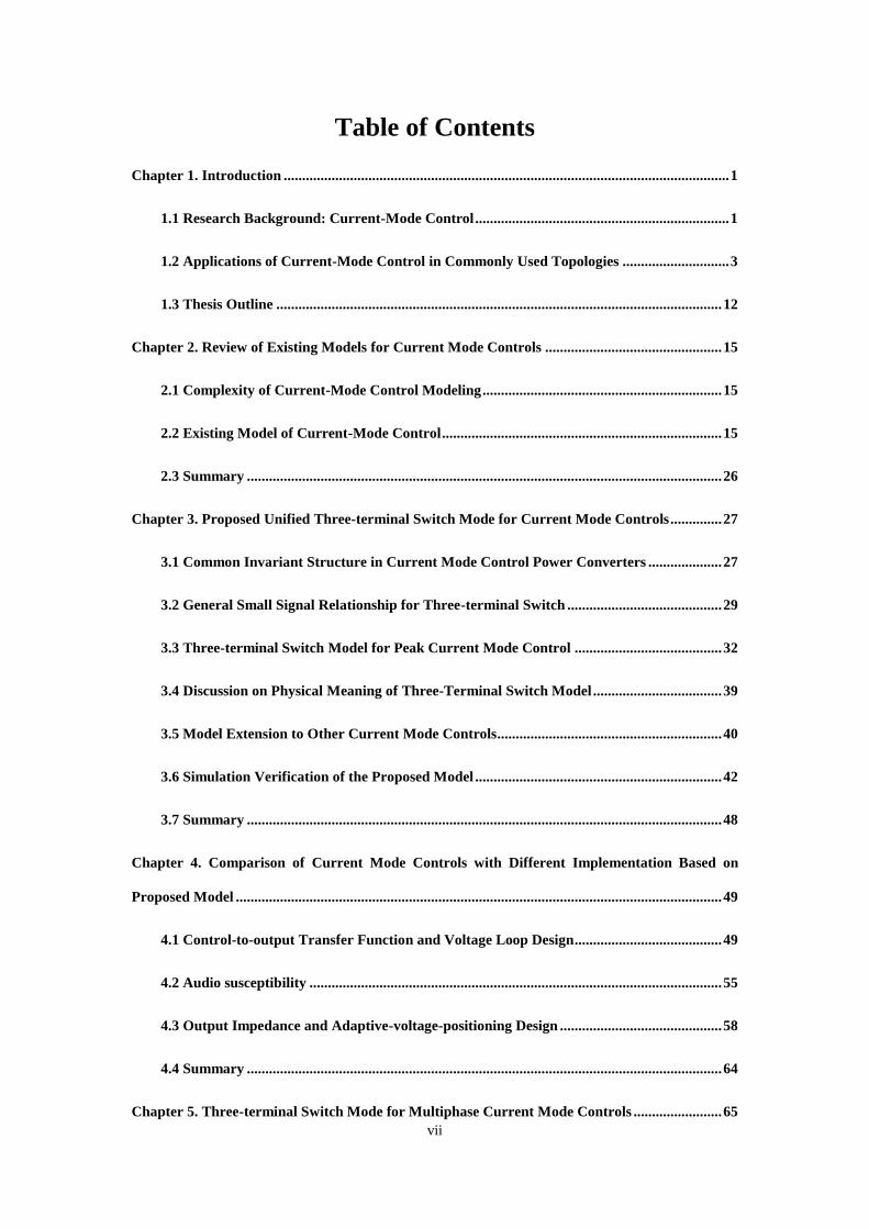
Table of Contents
Chapter 1. Introduction ......................................................................................................................... 1
1.1 Research Background: Current-Mode Control ..................................................................... 1
1.2 Applications of Current-Mode Control in Commonly Used Topologies ............................. 3
1.3 Thesis Outline ......................................................................................................................... 12
Chapter 2. Review of Existing Models for Current Mode Controls ................................................ 15
2.1 Complexity of Current-Mode Control Modeling ................................................................. 15
2.2 Existing Model of Current-Mode Control ............................................................................ 15
2.3 Summary ................................................................................................................................. 26
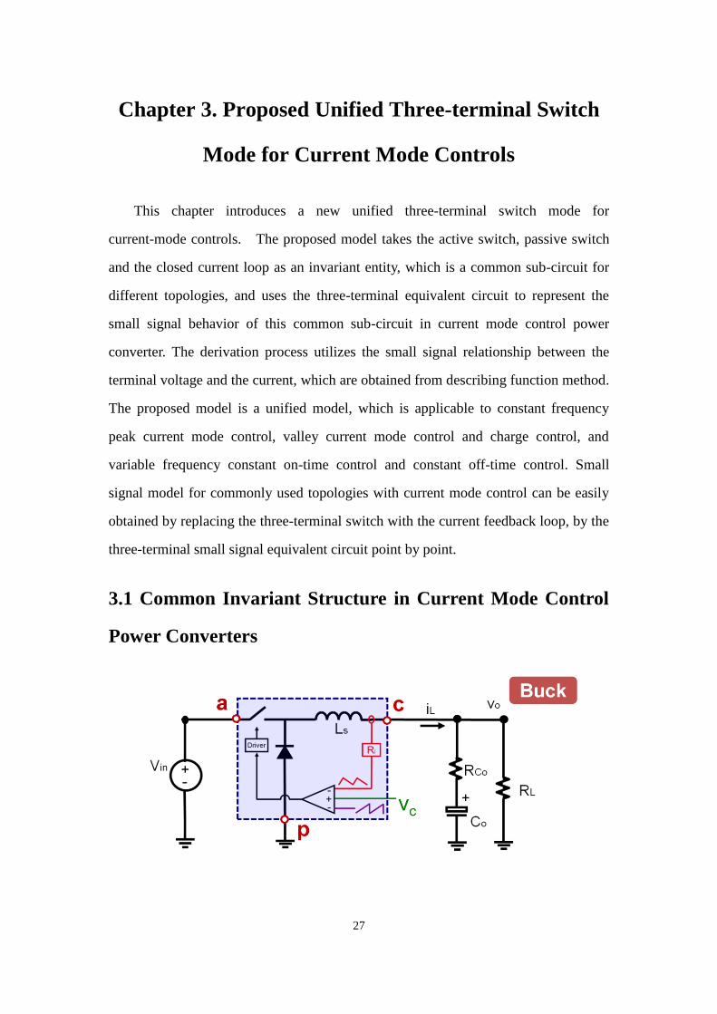
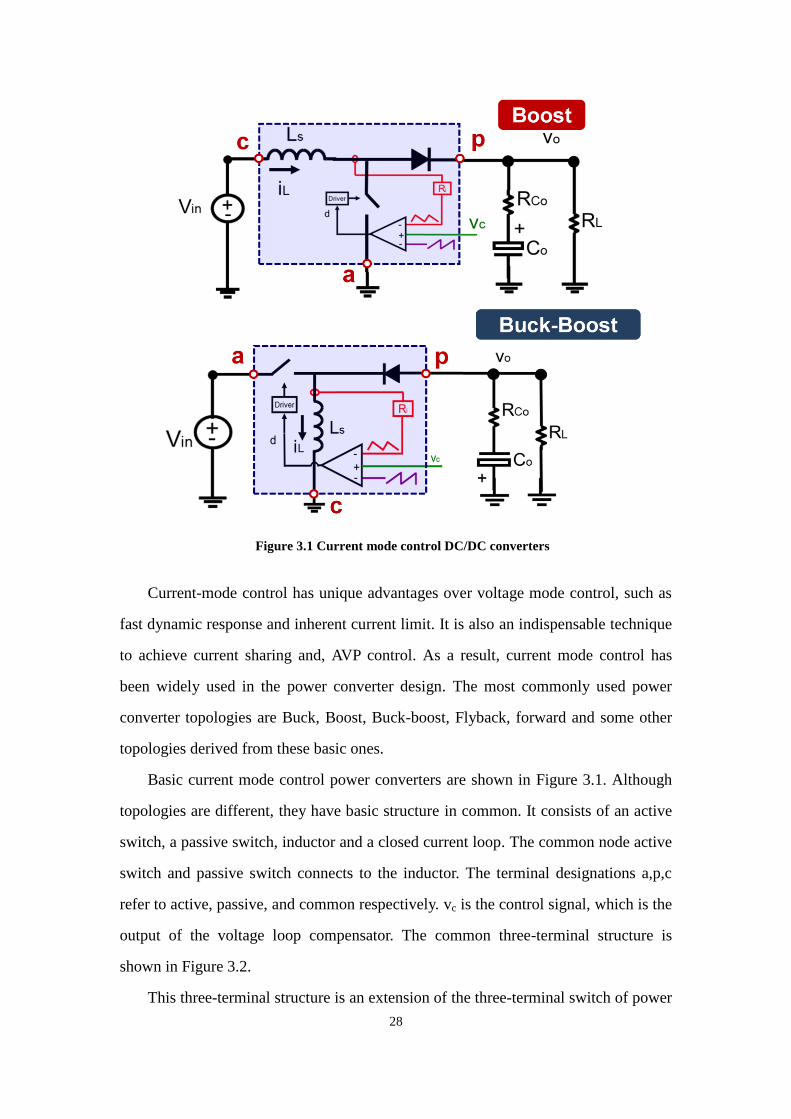
Chapter 3. Proposed Unified Three-terminal Switch Mode for Current Mode Controls .............. 27
3.1 Common Invariant Structure in Current Mode Control Power Converters .................... 27
3.2 General Small Signal Relationship for Three-terminal Switch .......................................... 29
3.3 Three-terminal Switch Model for Peak Current Mode Control ........................................ 32
3.4 Discussion on Physical Meaning of Three-Terminal Switch Model ................................... 39
3.5 Model Extension to Other Current Mode Controls ............................................................. 40
3.6 Simulation Verification of the Proposed Model ................................................................... 42
3.7 Summary ................................................................................................................................. 48
Chapter 4. Comparison of Current Mode Controls with Different Implementation Based on
Proposed Model .................................................................................................................................... 49
4.1 Control-to-output Transfer Function and Voltage Loop Design ........................................ 49
4.2 Audio susceptibility ................................................................................................................ 55
4.3 Output Impedance and Adaptive-voltage-positioning Design ............................................ 58
4.4 Summary ................................................................................................................................. 64
Chapter 5. Three-terminal Switch Mode for Multiphase Current Mode Controls ........................ 65
viii
5.1 Application of Multiphase Current Mode Control Power Converter ................................ 65
5.2 Three-terminal Switch Mode for Multiphase Current Mode Controls ............................. 67
5.3 Analysis of Small Signal Model for Multiphase Converter ................................................. 71
5.4 Feedback Design Consideration for Multi-phase Converter with Current Mode Control
........................................................................................................................................................ 75
5.5 Summary ................................................................................................................................. 78
Chapter 6. Conclusion .......................................................................................................................... 79
6.1 Summary ................................................................................................................................. 79
6.2 Future Works .......................................................................................................................... 80
Reference ............................................................................................................................................... 82

ix
List of Tables
Table 1.1 Typical high power LED specification ................................................................................... 11
Table 3. 1. Parameters Definition of Equivalent Circuit (Figure 3.7) .................................................... 34
Table 3. 2 Parameters Definition of Three-terminal Switch Model (Figure 3.12).................................. 41
Table 5.1. Parameters Definition of Figure 5.4 ...................................................................................... 68
Table 5.2. Parameters Definition of Figure 5.5 ...................................................................................... 69
x
List of Figures
Figure 1.1 Control structure of Current-mode control .............................................................................. 1
Figure 1.2. Different modulation schemes in current-mode control: (a) peak current-mode control, (b)
valley current mode control, (c) constant on-time control, (d) constant off-time control, and (e) charge
control ....................................................................................................................................................... 2
Figure 1. 3. A typical distributed power system ....................................................................................... 4
Figure 1. 4. A multi-phase buck converter with peak current-mode control ............................................ 5
Figure 1.5. Output impedance specification of Intel VRD 11.1 ............................................................... 5
Figure 1.6. Constant off-time current mode control CCM Boost PFC ..................................................... 6
Figure 1.7. Charge control Flyback PFC .................................................................................................. 7
Figure 1.8. Typical charge current and voltage profile ............................................................................. 8
Figure 1.9. Bi-directional Flyback charger and DC/DC converter ........................................................... 9
Figure 1. 10. Current mode control Buck LED driver ............................................................................ 11
Figure 2.1. current-mode control: (a) control structure, (b) “current source” concept ........................... 16
Figure 2.2. Average model for current-mode control with two additional feed forward gain and
feedback gain .......................................................................................................................................... 17
Figure 2.3. Control-to-output transfer function comparison (D=0.45) ................................................ 18
Figure 2.4. Discrete-time analysis: (a) natural response, and (b) forced response .............................. 18
Figure 2.5. R. Ridley’ model for peak current-mode control .............................................................. 21
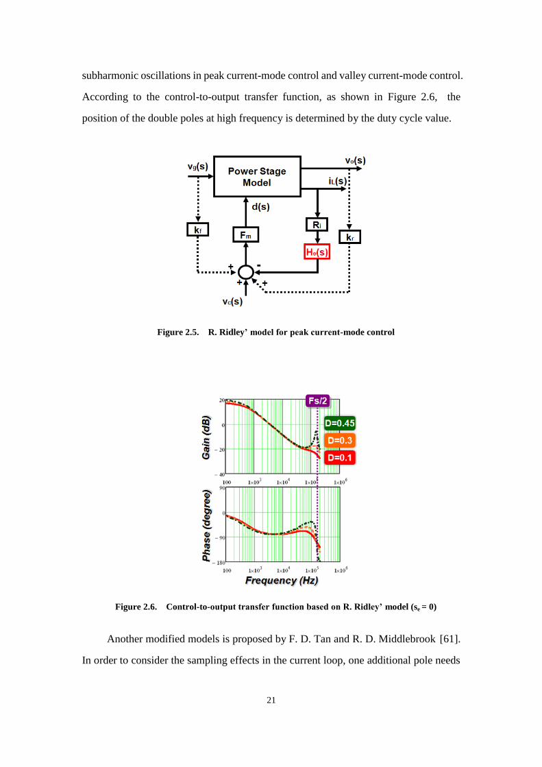
Figure 2.6. Control-to-output transfer function based on R. Ridley’ model (se = 0) ............................ 21
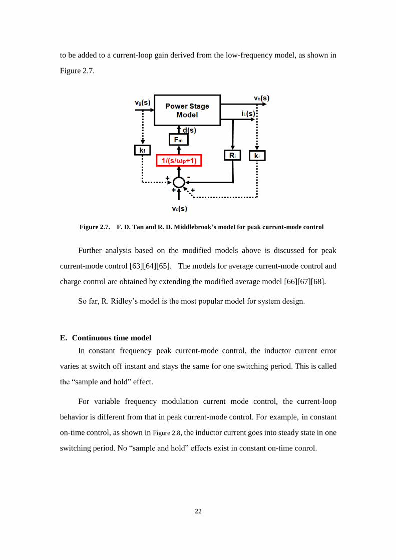
Figure 2.7. F. D. Tan and R. D. Middlebrook’s model for peak current-mode control ....................... 22
Figure 2.8. Perturbed inductor current waveform: (a) in peak current-mode control, and (b) in
constant on-time control ......................................................................................................................... 23
Figure 2.9. Discrepancy in the extended model ................................................................................... 23
xi
Figure 2.10. Perturbed inductor current waveform in peak current-mode control ................................. 24
Figure 2.11. Equivalent circuit for current mode control Buck converter .............................................. 25
Figure 3.1 Current mode control DC/DC converters .............................................................................. 28
Figure 3.2 Common invariant structure in current mode control power converters ............................... 29
Figure 3.3 Basic waveform of PWM switch .......................................................................................... 30
Figure 3.4 Duty cycle to switch current transfer function (fixed frequency modulation) ...................... 31
Figure 3.5 Duty cycle to switch current transfer function(variable frequency modulation) ................... 32
Figure 3.6 Current mode control Buck converter ................................................................................... 33
Figure 3.7 Equivalent circuit for current mode control Buck converter ................................................. 34
Figure 3.8 Equivalent circuit with DC transformer ................................................................................ 36
Figure 3.9 Complete equivalent circuit for peak current mode control Buck converter ......................... 38
Figure 3.10 Three terminal equivalent circuit model for peak current mode control ............................. 38
Figure 3.11 Three terminal equivalent circuit model degenerates to three-terminal switch mode for the
power stage when se>>sn,sf ..................................................................................................................... 40
Figure 3.12 Unified three terminal equivalent circuit model for current mode controls ........................ 41
Figure 3.13 Simulation verification of control-to-output and input-to-output transfer function for peak
current mode control Buck converter ..................................................................................................... 43
Figure 3.14 Simulation verification of output impedance and input impedance for peak current mode
control Buck converter ........................................................................................................................... 43
Figure 3.15 Peak current mode control Boost converter and its small signal equivalent circuit ............ 44
Figure 3.16 Simulation verification of control-to-output and input-to-output transfer function for peak
current mode control Boost converter .................................................................................................... 45
Figure 3.17 Simulation verification of output impedance and input impedance for peak current mode
control Boost converter .......................................................................................................................... 45
Figure 3.18 Charge control Flyback converter and its small signal equivalent ...................................... 46

xii
Figure 3.20 Simulation verification of control-to-output and input-to-output transfer function for
constant on-time current mode control Buck converter .......................................................................... 47
Figure 3.21 Simulation verification of input impedance and output impedance for constant on-time
current mode control Buck converter ..................................................................................................... 48
Figure 4.1 Pole-zero map comparison in low duty cycle case ................................................................ 51
Figure 4.2 Control-to-output transfer function comparison .................................................................... 52
Figure 4.3. Equivalent circuit of Buck converter with outer feedback loop ........................................... 53
Figure 4.4 T2 loop gain comparison: constant on-time, constant off-time and peak current mode control
................................................................................................................................................................ 53
Figure 4.5 Pole-zero map comparison in large duty cycle case .............................................................. 54
Figure 4.6 T2 loop gain comparison: constant on-time, constant off-time and valley current mode
control ..................................................................................................................................................... 55
Figure 4.7 Simulation result of constant off-time control under input perturbation ............................... 58
Figure 4.8 Definition of output impedance with closed current loop ..................................................... 59
Figure 4.9 Open loop output impedance of current mode control .......................................................... 60
Figure 4.10. Load-line specification of Intel VRD 11.0 ......................................................................... 60
Figure 4.11 Constant output impedance design target and desired T2 ................................................... 61
Figure 4.12 Compensator design for peak current mode control ............................................................ 62
Figure 4.13 Compensator design for constant on-time current mode control......................................... 63
Figure 4.14 Simulation result of output impedance of constant on-time current mode control.............. 63
Figure 4.15 Simulation result for the transient response with constant on-time current mode control .. 64
Figure 5.1 Multiphase interleave Buck converter ................................................................................... 66
Figure 5.2 Multiphase interleave Boost PFC .......................................................................................... 66
Figure 5.3 Multiphase interleave current mode control Buck converter ................................................ 67
xiii
Figure 5.4 Equivalent circuit for multiphase Buck converter ................................................................. 68
(N single phase equivalent circuit in parallel) ........................................................................................ 68
Figure 5.5 Equivalent circuit for multiphase Buck converter ................................................................. 69
(Equivalent single phase representation) ................................................................................................ 69
Figure 5.6 Control-to-output transfer function of 2-phase Buck converter ............................................ 71
Figure 5.7 Comparison of control-to-output transfer function: single phase vs. 2-phase ....................... 72
Figure 5.8 Control-to-output transfer function of different phase shift angles ....................................... 73
Figure 5.9 Comparison of input-to-output transfer function: single phase vs. 2-phase .......................... 74
Figure 5.10 Comparison of T2 loop gain: single phase vs. 2-phase ....................................................... 76
Figure 5.11 Output impedance of single phase Buck ............................................................................. 77
Figure 5.12 Output impedance of single phase Buck and 2-phase Buck ................................................ 77
1
Chapter 1. Introduction
1.1 Research Background: Current-Mode Control
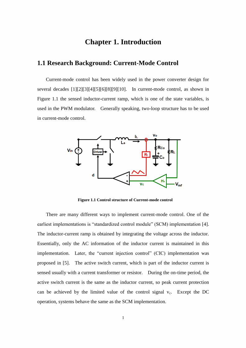
Current-mode control has been widely used in the power converter design for
several decades [1][2][3][4][5][6][8][9][10]. In current-mode control, as shown in
Figure 1.1 the sensed inductor-current ramp, which is one of the state variables, is
used in the PWM modulator. Generally speaking, two-loop structure has to be used
in current-mode control.
Figure 1.1 Control structure of Current-mode control
There are many different ways to implement current-mode control. One of the
earliest implementations is “standardized control module” (SCM) implementation [4].
The inductor-current ramp is obtained by integrating the voltage across the inductor.
Essentially, only the AC information of the inductor current is maintained in this
implementation. Later, the “current injection control” (CIC) implementation was
proposed in [5]. The active switch current, which is part of the inductor current is
sensed usually with a current transformer or resistor. During the on-time period, the
active switch current is the same as the inductor current, so peak current protection
can be achieved by the limited value of the control signal vc. Except the DC
operation, systems behave the same as the SCM implementation.
2
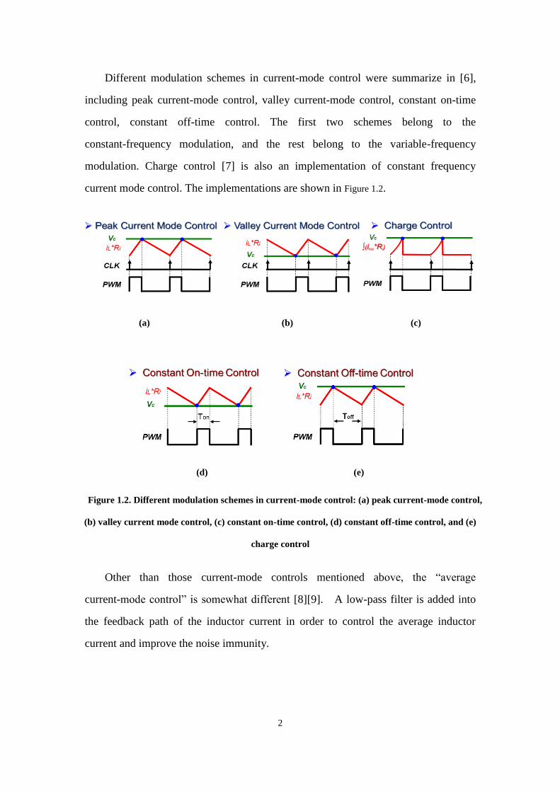
Different modulation schemes in current-mode control were summarize in [6],
including peak current-mode control, valley current-mode control, constant on-time
control, constant off-time control. The first two schemes belong to the
constant-frequency modulation, and the rest belong to the variable-frequency
modulation. Charge control [7] is also an implementation of constant frequency
current mode control. The implementations are shown in Figure 1.2.
(a) (b) (c)
(d) (e)
Figure 1.2. Different modulation schemes in current-mode control: (a) peak current-mode control,
(b) valley current mode control, (c) constant on-time control, (d) constant off-time control, and (e)
charge control
Other than those current-mode controls mentioned above, the “average
current-mode control” is somewhat different [8][9]. A low-pass filter is added into
the feedback path of the inductor current in order to control the average inductor
current and improve the noise immunity.
3
1.2 Applications of Current-Mode Control in Commonly
Used Topologies
Due to its unique characteristics, current-mode control is indispensable to power
converter design in almost every aspect. A few applications of current-mode control
are introduced in the following paragraphs.
1.2.1 Voltage Regulator Application
With the development of information technology, telecom, computer and
network systems have become a large market for the power supply industry [11].
Power supplies for the telecom, computer and network applications are required to
provide more power with less size and cost [12][13]. To meet these requirements,
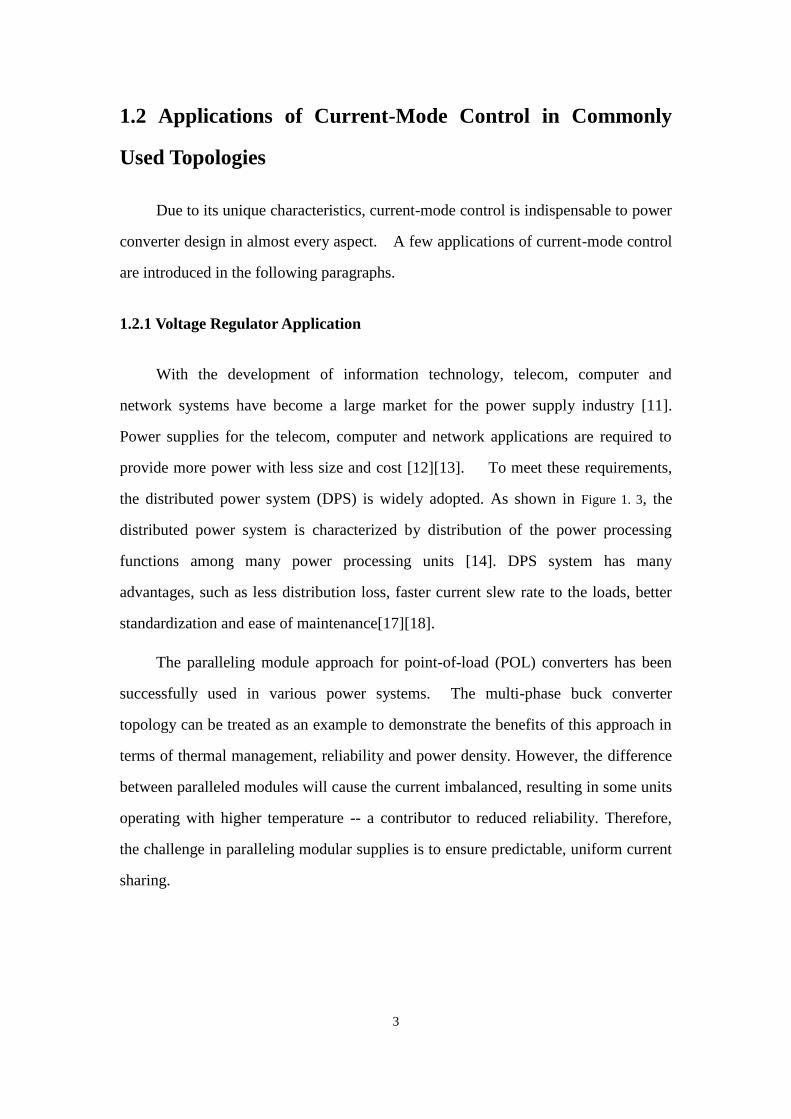
the distributed power system (DPS) is widely adopted. As shown in Figure 1. 3, the
distributed power system is characterized by distribution of the power processing
functions among many power processing units [14]. DPS system has many
advantages, such as less distribution loss, faster current slew rate to the loads, better
standardization and ease of maintenance[17][18].
The paralleling module approach for point-of-load (POL) converters has been
successfully used in various power systems. The multi-phase buck converter
topology can be treated as an example to demonstrate the benefits of this approach in
terms of thermal management, reliability and power density. However, the difference
between paralleled modules will cause the current imbalanced, resulting in some units
operating with higher temperature -- a contributor to reduced reliability. Therefore,
the challenge in paralleling modular supplies is to ensure predictable, uniform current
sharing.
4
Figure 1. 3. A typical distributed power system
There are many methods to achieve current sharing among different modules
(phases). One of the most popular methods is the active current sharing method with
current-mode control [19]. As shown in Figure 1. 4, a current sharing bus is easily
built by the control signal in peak current-mode control. It usually provides a
common current reference. Each phase then adjusts its own control to follow this
common reference thus the load current will finally evenly distributed among these
phases.
In order to provide power to a microprocessor with high current and low voltage
demand, a dedicated power supply named voltage regulator (VR) is used. Multi-phase
buck converters are widely used in VRs because of their simple structure, low cost
and low conduction loss. Current VR faces the stringent challenge of not only high
current but also a strict transient response requirement. Figure 1.5 shows the VR output
load line from the Intel VRD 11.1 specification. The vertical axis is the VR output
impedance, and the horizontal axis is frequency.
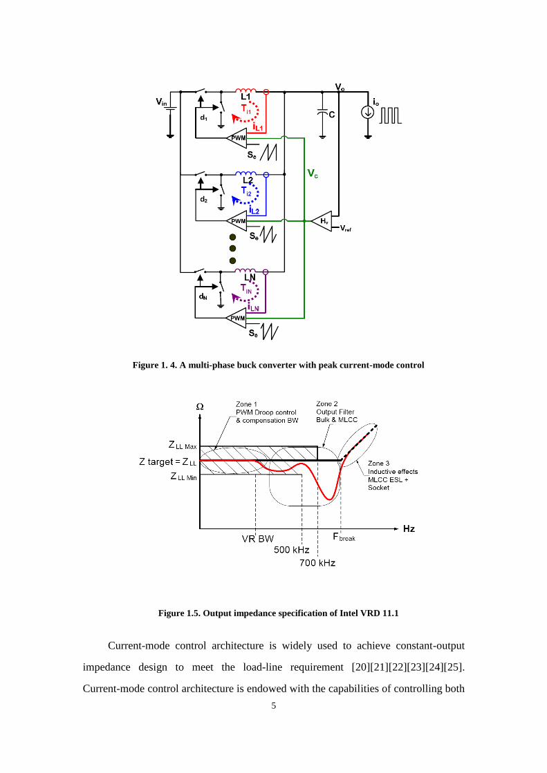
5
Figure 1. 4. A multi-phase buck converter with peak current-mode control
Figure 1.5. Output impedance specification of Intel VRD 11.1
Current-mode control architecture is widely used to achieve constant-output
impedance design to meet the load-line requirement [20][21][22][23][24][25].
Current-mode control architecture is endowed with the capabilities of controlling both
6
the output voltage and the inductor current, which is one of key factors to achieve
AVP control.
1.2.2. Power factor correction
Due to the ever-increasing requirement for improved power quality, the use of the
power factor correction (PFC) circuit for off line power supplies has been
dramatically increased. The high frequency switch mode power factor correction
converter is called a PFC stage and, it is usually inserted in the equipment to shape the
line input current into a sinusoidal waveform and its line current is in phase with the
line voltage.
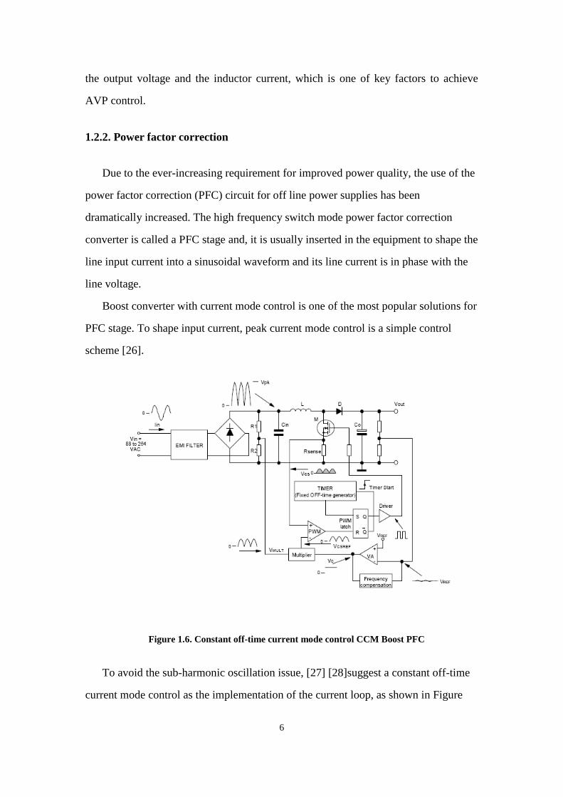
Boost converter with current mode control is one of the most popular solutions for
PFC stage. To shape input current, peak current mode control is a simple control
scheme [26].
Figure 1.6. Constant off-time current mode control CCM Boost PFC
To avoid the sub-harmonic oscillation issue, [27] [28]suggest a constant off-time
current mode control as the implementation of the current loop, as shown in Figure
7
1.6. Constant off-time control is a variable frequency control scheme, so it also helps
to reduce the peak energy of the noise generated and simplifies the ability to comply
with EMI regulations.
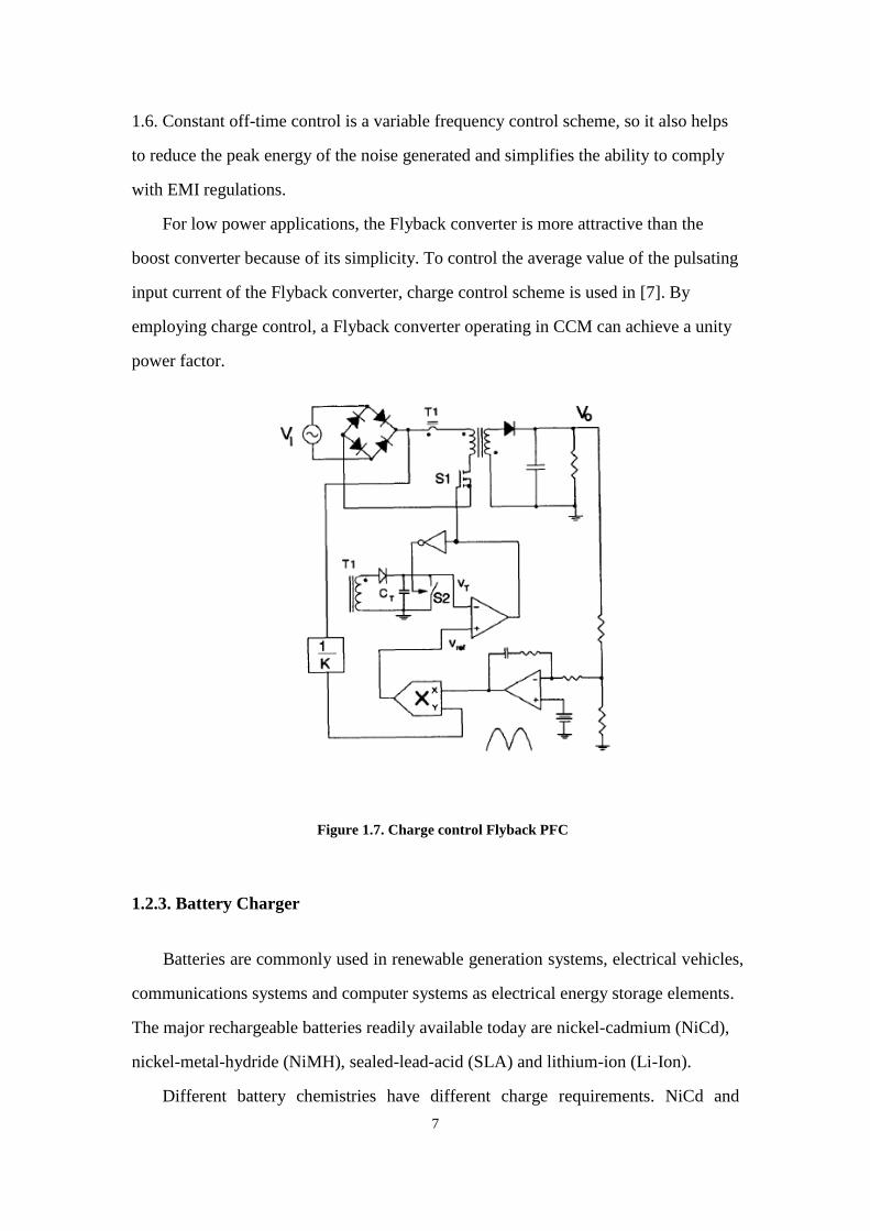
For low power applications, the Flyback converter is more attractive than the
boost converter because of its simplicity. To control the average value of the pulsating
input current of the Flyback converter, charge control scheme is used in [7]. By
employing charge control, a Flyback converter operating in CCM can achieve a unity
power factor.
Figure 1.7. Charge control Flyback PFC
1.2.3. Battery Charger
Batteries are commonly used in renewable generation systems, electrical vehicles,
communications systems and computer systems as electrical energy storage elements.
The major rechargeable batteries readily available today are nickel-cadmium (NiCd),
nickel-metal-hydride (NiMH), sealed-lead-acid (SLA) and lithium-ion (Li-Ion).
Different battery chemistries have different charge requirements. NiCd and
8
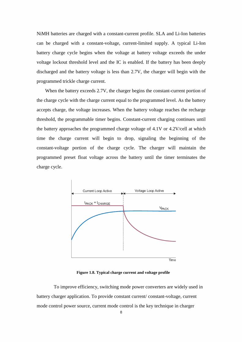
NiMH batteries are charged with a constant-current profile. SLA and Li-Ion batteries
can be charged with a constant-voltage, current-limited supply. A typical Li-Ion
battery charge cycle begins when the voltage at battery voltage exceeds the under
voltage lockout threshold level and the IC is enabled. If the battery has been deeply
discharged and the battery voltage is less than 2.7V, the charger will begin with the
programmed trickle charge current.
When the battery exceeds 2.7V, the charger begins the constant-current portion of
the charge cycle with the charge current equal to the programmed level. As the battery
accepts charge, the voltage increases. When the battery voltage reaches the recharge
threshold, the programmable timer begins. Constant-current charging continues until
the battery approaches the programmed charge voltage of 4.1V or 4.2V/cell at which
time the charge current will begin to drop, signaling the beginning of the
constant-voltage portion of the charge cycle. The charger will maintain the
programmed preset float voltage across the battery until the timer terminates the
charge cycle.
Figure 1.8. Typical charge current and voltage profile
To improve efficiency, switching mode power converters are widely used in
battery charger application. To provide constant current/ constant-voltage, current
mode control power source, current mode control is the key technique in charger
9
controller.
The typical operation of the battery charger can be separate into two periods [29].
The charge current-regulation loop is in control as long as the battery voltage is below
the set point. When the battery voltage reaches its set point, the voltage-regulation
loop takes control and maintains the battery voltage at the set point. The typical
charge current and voltage profile is shown in Figure 1.8.
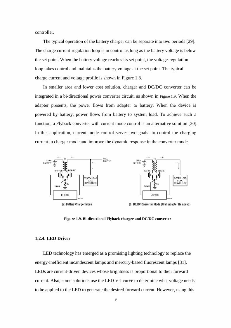
In smaller area and lower cost solution, charger and DC/DC converter can be
integrated in a bi-directional power converter circuit, as shown in Figure 1.9. When the
adapter presents, the power flows from adapter to battery. When the device is
powered by battery, power flows from battery to system load. To achieve such a
function, a Flyback converter with current mode control is an alternative solution [30].
In this application, current mode control serves two goals: to control the charging
current in charger mode and improve the dynamic response in the converter mode.
Figure 1.9. Bi-directional Flyback charger and DC/DC converter
1.2.4. LED Driver
LED technology has emerged as a promising lighting technology to replace the
energy-inefficient incandescent lamps and mercury-based fluorescent lamps [31].
LEDs are current-driven devices whose brightness is proportional to their forward
current. Also, some solutions use the LED V-I curve to determine what voltage needs
to be applied to the LED to generate the desired forward current. However, using this
10
method, any change in LED forward voltage creates a change in LED current. At the
same time, the voltage drop and power dissipation across the ballast resistor waste
power and reduce battery life.
Most of the high performance LED drivers drive the LED with a constant-current
source. In this way, forward voltage does not affect LED brightness. Many
applications, such as display backlighting, need more than one LED to provide
enough brightness. In these applications, multiple LEDs should be connected in a
series configuration to keep an identical current flowing in each LED.
Since Buck converter output current is an inductor current, a non-pulsating
current, Buck converter without output capacitor is widely used as a LED driver due
to its simple structure, low cost and fast response. In a Buck converter without output
capacitor, controlling inductor current is controlling the LED forward current. So,
current mode control is a natural choice for Buck LED driver.
Based on the characteristics of LED, all LEDs have a relationship between their
luminous flux and forward current, IF, that is linear up to a point. Beyond that point,
increasing IF causes more heat than light. High ripple current forces the LED to spend
half of the time at a high peak current, putting it in the lower lm/W region of the flux
curve. Usually, absolute maximum ratings for peak current are close to or often equal
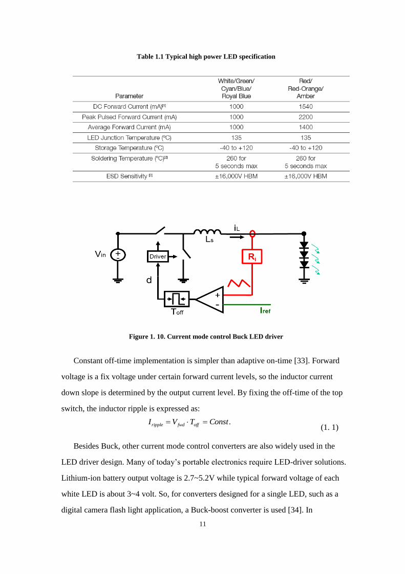
to the ratings for average current, as shown in Table 1.1 [32]. High current density in
the LED junction lowers lumen maintenance, providing yet another incentive for
keeping the ripple current under control.
To achieve a constant forward current ripple, adaptive on time and constant
off-time current mode control implementation is a common solution. Adaptive on
time control changes the top switch on-time to be proportional to Vin-Vout, so that
the current ripple is kept constant with input voltage variation.
11
Table 1.1 Typical high power LED specification
Figure 1. 10. Current mode control Buck LED driver
Constant off-time implementation is simpler than adaptive on-time [33]. Forward
voltage is a fix voltage under certain forward current levels, so the inductor current
down slope is determined by the output current level. By fixing the off-time of the top
switch, the inductor ripple is expressed as:
.ConstTVI offfwdripple (1. 1)
Besides Buck, other current mode control converters are also widely used in the
LED driver design. Many of today’s portable electronics require LED-driver solutions.
Lithium-ion battery output voltage is 2.7~5.2V while typical forward voltage of each
white LED is about 3~4 volt. So, for converters designed for a single LED, such as a
digital camera flash light application, a Buck-boost converter is used [34]. In
12
backlighting application, to drive a series of white LEDs with a constant current
source, a popular solution is to use a Boost or Buck-boost converter with current
mode control [35].
1.3 Thesis Outline
Current-mode control architectures with different implementation approaches
have been an indispensable technique in many applications, such as voltage regulator,
power factor correction, battery charger and LED driver. Since the inductor current
ramp, one of state variables influenced by the input voltage and the output voltage, is
used in the modulator in current-mode control without any low pass filter, high order
harmonics play important role in the feedback control. This is the reason for the
difficulty in obtaining the small-signal model for current-mode control in the
frequency domain. A continuous time domain model was recently proposed as a
successful model for the current-mode control architectures with different
implementation. However, the model was derived by describing function method,
which is very complicated arithmetically, not to mention time consuming. Although
an equivalent circuit for the current mode control Buck converter was proposed to
help designers to use the model without involving complicated math, the equivalent
circuit is not a complete model. Moreover, no equivalent circuit for other topologies is
available for designers. In this thesis, the primary objective is to develop a unified
three-terminal switch model for current-mode control with different implementation
methods which are applicable in all the current mode control power converters. First,
the existing model for current mode control is reviewed. After that, a unified
three-terminal switch model for current mode control is proposed. Then, based on the
proposed unified model, a comparison between different current mode control
implementation is presented. At last, the model is extended to multiphase current
mode control. Some design concerns are discussed based on the model. In the end,
conclusions are given.
13
The detailed outline is elaborated as follows.
Chapter 1 is the review of the background of current-mode control and the
application of current-mode control. Current-mode control architectures with
different implementation approaches have been an indispensable technique in many
applications, such as voltage regulator, power factor correction, battery charger and
LED driver. An accurate model for current-mode control is indispensable to system
design. However, available models can only solve partial issues. The primary
objective of this thesis is to develop a unified three-terminal switch model for
current-mode control with different implementation methods which is applicable in all
the current mode control power converters.
In Chapter 2, the existing model for current mode control is reviewed. The
limitation of average models and discrete time model for current-mode control is
identified. The continuous time model and its equivalent circuit of Buck converter is
introduced. The deficiency of the equivalent circuit is discussed.
In Chapter 3, a unified three-terminal switch model for current mode control is
presented. Based on the observation, the PWM switch and the closed current loop is
taken as an invariant sub-circuit which is common to different DC/DC converter
topologies. The Basic small signal relationship is studied and the result shows that the
PWM switch with current feedback preserves the property of the PWM switch in
power stage. A three-terminal equivalent circuit is developed to represent the small
signal behavior of this common sub-circuit. The proposed model is a unified model,
which is applicable in both constant frequency modulation and variable frequency
modulation. The physical meaning of the three-terminal equivalent circuit model is
discussed. The model is verified by SIMPLIS simulation in commonly used
converters for both constant frequency modulation and variable frequency
modulation.
In Chapter 4, based on the proposed unified model, a comparison between
different current mode control implementation is presented. In different applications,

14
different implementations have unique benefit of extending control bandwidth in
different applications. The properties of audio susceptibility and output impedance are
discussed. It is found that, for adaptive voltage positioning design, constant on-time
current mode control can simplified the outer loop design.
In Chapter 5, since multiphase interleaving structure is widely used in PFC,
voltage regulator and other high current application, the model is extended to the
multiphase current mode control. Some design concerns are discussed based on the
model.
Chapter 6 is conclusions with the summary and the future work.
15
Chapter 2. Review of Existing Models for Current
Mode Controls
2.1 Complexity of Current-Mode Control Modeling
Current-mode control’s modulation is based on the inductor current ramp, a state
variable. Essentially, for any PWM converter with a small signal perturbation fm, the
PWM modulator generates multiple frequency components, including the
fundamental component (fm), the switching frequency component (fs) and its
harmonic (n*fs), and the sideband components (fs±fm, nfs±fm). All these frequency
components exist in the state variable of the switching circuit. In current mode control
case, inductor current is fed back to the modulator, and there is no enough attenuation
on the high frequency components. All frequency components are coupled through the
modulator, so neither the sideband components nor the switching frequency
components can be ignored. As a result, frequency domain analysis shows its obvious
limitation in analysis of current loop. Previous average models for current-mode
control failed to consider high frequency components.
It is relatively easy for the outer voltage loop of the current mode control
converter, since high frequency components can be attenuated due to the low pass
filter of the power stage and feedback compensation.
2.2 Existing Model of Current-Mode Control
Due to the popularity of the current-mode control and the complexity of the
current mode control, the research on modeling current-mode control has over 30
years of history and is still on going.
Most of the early work on current mode control modeling focuses on peak
current mode control due to its popularity. In recent decades, variable frequency
16
current mode control, for example constant on-time control, is widely used because of
its unique advantage, such as high light load efficiency and simple implementation.
The modeling of variable frequency current mode control has gained more attention
recently.
To review the previous modeling work for current mode control, the modeling
methodologies can be categorized into several groups and listed as follows.
A. “Current source” model
The purpose of the current loop is to make the inductor current follow the
control signal. Based on this physical interpretation, the “current-source” concept is
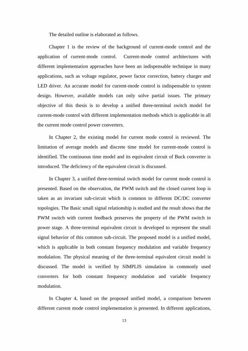
the simplest model for model current-mode control [36]. In this model, the inductor
current is treated as a well-controlled current source, as shown in Figure 2.1. However,
it is too simple to predict subharmonic oscillations and the audio susceptibility.
(a)
Figure 2.1. current-mode control: (a) control structure, (b) “current source” concept
B. Average model
Under purturbation, although a switching converter generates many side band
components, since there must be a low-pass filter in the power stage, the average
17
concept, which only capture the modulation frequency information, can be sucessfully
used in the modeling of the switching converter[37][38][39][55][40][41][42][43].
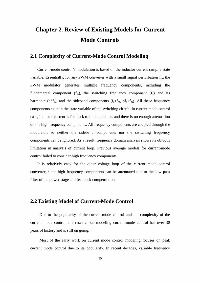
Based on average models for power stage, the average models for peak current-mode
control are developed[44] [45][46][47][48][49][50][51][52][53][54].
Figure 2.2. Average model for current-mode control with two additional feed forward gain and
feedback gain
In the current loop, averaged inductor-current information is fed back to the
modulator with pure sensing gain. Modulator gain Fm, is derived by geometrical
calculations, assuming a constant inductor current ramp and an external ramp. In
order to model the effect of the variation of the inductor current ramp, two additional
feed forward gain and feedback gain are added [45].
The low-frequency response can be well predicted by the average models.
However, one common issue of the average models is that they can’t predict
subharmonic oscillations in peak current-mode control, as shown in Figure 2.3.
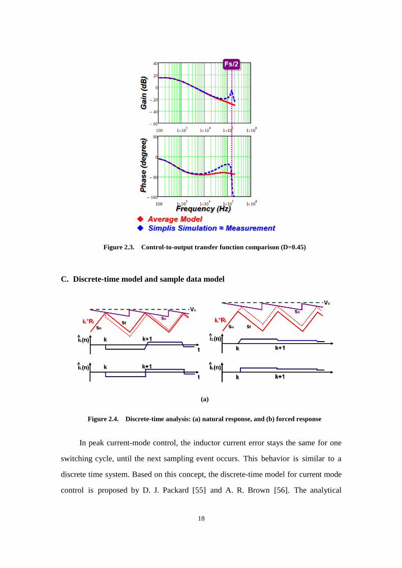
18
Figure 2.3. Control-to-output transfer function comparison (D=0.45)
C. Discrete-time model and sample data model
(a)
Figure 2.4. Discrete-time analysis: (a) natural response, and (b) forced response
In peak current-mode control, the inductor current error stays the same for one
switching cycle, until the next sampling event occurs. This behavior is similar to a
discrete time system. Based on this concept, the discrete-time model for current mode
control is proposed by D. J. Packard [55] and A. R. Brown [56]. The analytical
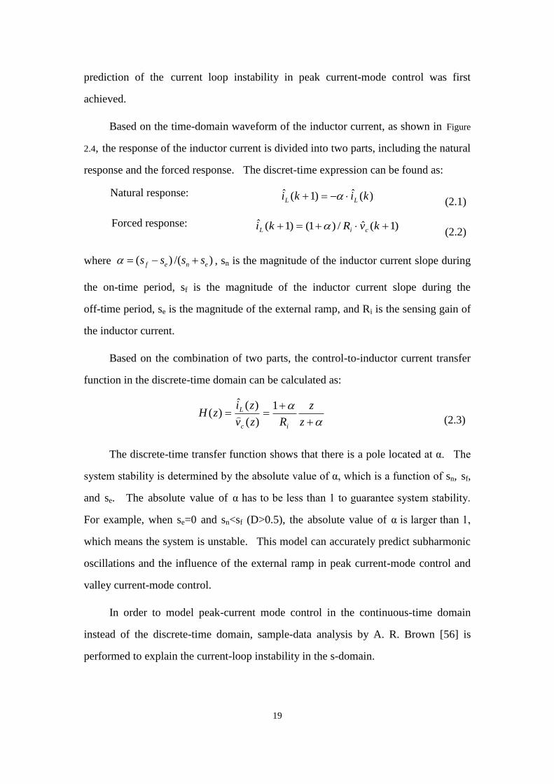
19
prediction of the current loop instability in peak current-mode control was first
achieved.
Based on the time-domain waveform of the inductor current, as shown in Figure
2.4, the response of the inductor current is divided into two parts, including the natural
response and the forced response. The discret-time expression can be found as:
Natural response: )(ˆ)1(ˆ kiki LL (2.1)
Forced response: )1(ˆ/)1()1(ˆ kvRki ciL (2.2)
where )/()( enef ssss , sn is the magnitude of the inductor current slope during
the on-time period, sf is the magnitude of the inductor current slope during the
off-time period, se is the magnitude of the external ramp, and Ri is the sensing gain of
the inductor current.
Based on the combination of two parts, the control-to-inductor current transfer
function in the discrete-time domain can be calculated as:
z
z
Rzv
zizH
ic
L 1
)(
)(ˆ)( (2.3)
The discrete-time transfer function shows that there is a pole located at α. The
system stability is determined by the absolute value of α, which is a function of sn, sf,
and se. The absolute value of α has to be less than 1 to guarantee system stability.
For example, when se=0 and sn<sf (D>0.5), the absolute value of α is larger than 1,
which means the system is unstable. This model can accurately predict subharmonic
oscillations and the influence of the external ramp in peak current-mode control and
valley current-mode control.
In order to model peak-current mode control in the continuous-time domain
instead of the discrete-time domain, sample-data analysis by A. R. Brown [56] is
performed to explain the current-loop instability in the s-domain.
20
Although the discrete-time model and sampled-data model can precisely predict
the high-freqeuncy response, it is hard to use, just like the discrete-time model.
D. Modified average model
In order to extend the validation of the averaged models to the high-frequency
range, several modified average models are proposed based on the results of
discrete-time analysis and sample-data analysis [57][58][59][60][61][62][63][64][65].
One of popular models is investigated by R. Ridley [59], which provided both the
accuracy of the sample-data model and the simplicity of the three-terminal switch
model. Essentially, R. Ridley’s modeling strategy is based on the hypothesis method.
In this method, first, the control-to-inductor current transfer function is obtained by
transferring previous accurate disctrete-time transfer function (2.3) into its
continuous-time form:
sw
sw
sT
sT
swic
L
e
e
sTRsv
si 111
)(
)(
(2.4)
Then, “sample and hold” effects are equivalently represented by the He(s)
function which is inserted into the feedback path of the inductor current in the
continuous avarge model, as shown in Figure 2.5. Another form of the
control-to-inductor current transfer function can be calculated based on this assumed
average model:
)()(1
)(
)(
)(
sHRsFF
sFF
sv
si
eiim
im
c
L
(2.5)
Finally, based on (2.4) and (2.5), the He(s) function is obtained as
1)(
swsT
swe
e
sTsH
(2.6)
Following the same concept used in [45], the complete model is completed by
adding two additional feed-forward gain and feedback gain. Due to its origination
from the discrtete-time model, there is no doubt that this model can accurately predict
21
subharmonic oscillations in peak current-mode control and valley current-mode control.
According to the control-to-output transfer function, as shown in Figure 2.6, the
position of the double poles at high frequency is determined by the duty cycle value.
Figure 2.5. R. Ridley’ model for peak current-mode control
Figure 2.6. Control-to-output transfer function based on R. Ridley’ model (se = 0)
Another modified models is proposed by F. D. Tan and R. D. Middlebrook [61].
In order to consider the sampling effects in the current loop, one additional pole needs
22
to be added to a current-loop gain derived from the low-frequency model, as shown in
Figure 2.7.
Figure 2.7. F. D. Tan and R. D. Middlebrook’s model for peak current-mode control
Further analysis based on the modified models above is discussed for peak
current-mode control [63][64][65]. The models for average current-mode control and
charge control are obtained by extending the modified average model [66][67][68].
So far, R. Ridley’s model is the most popular model for system design.
E. Continuous time model
In constant frequency peak current-mode control, the inductor current error
varies at switch off instant and stays the same for one switching period. This is called
the “sample and hold” effect.
For variable frequency modulation current mode control, the current-loop
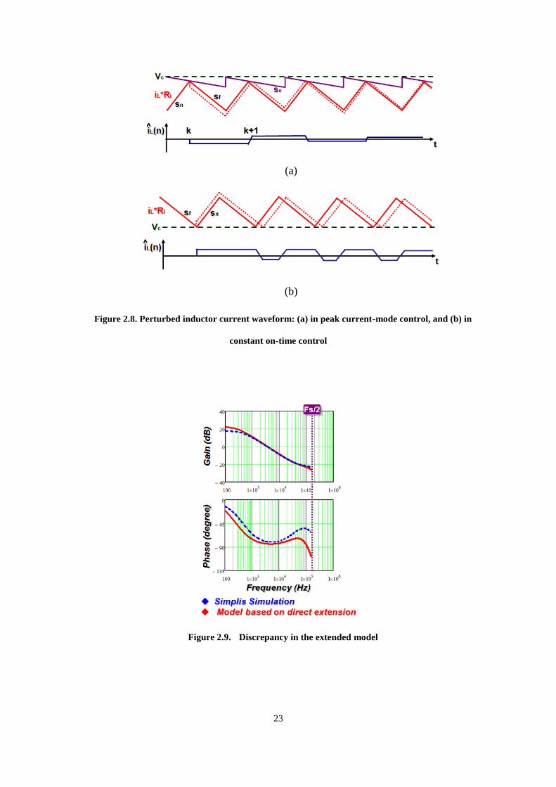
behavior is different from that in peak current-mode control. For example, in constant
on-time control, as shown in Figure 2.8, the inductor current goes into steady state in one
switching period. No “sample and hold” effects exist in constant on-time conrol.
23
(a)
(b)
Figure 2.8. Perturbed inductor current waveform: (a) in peak current-mode control, and (b) in
constant on-time control
Figure 2.9. Discrepancy in the extended model
24
Discrete-time analsys and sample-data analysis is only applicable to a constant
frequency sampling system. They can’t be applied to variable frequency current mode
control. Figure 2.9 shows that R. Ridley’s extended model to constant on-time control
[69] is not very good at predicting the small signal behavior of the switching circuit.
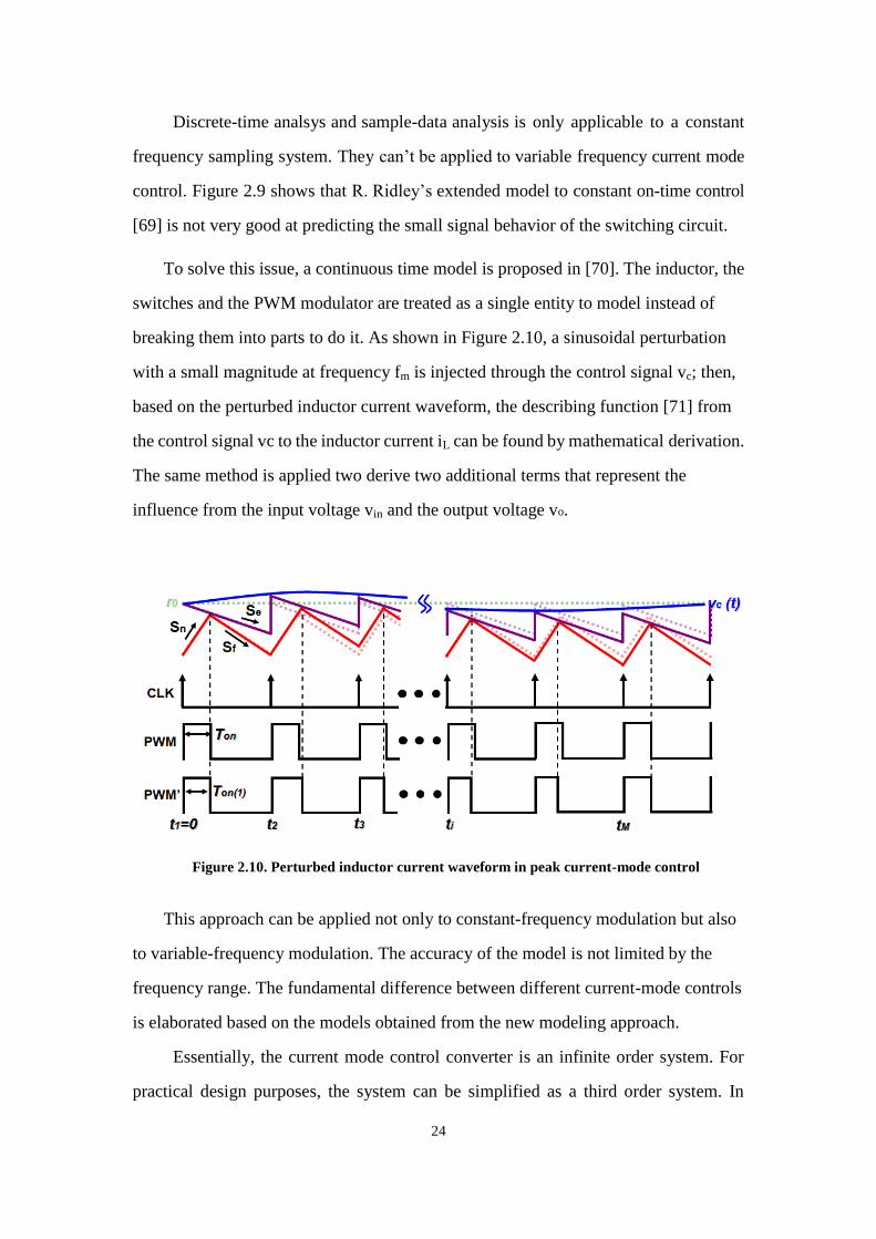
To solve this issue, a continuous time model is proposed in [70]. The inductor, the
switches and the PWM modulator are treated as a single entity to model instead of
breaking them into parts to do it. As shown in Figure 2.10, a sinusoidal perturbation
with a small magnitude at frequency fm is injected through the control signal vc; then,
based on the perturbed inductor current waveform, the describing function [71] from
the control signal vc to the inductor current iL can be found by mathematical derivation.
The same method is applied two derive two additional terms that represent the
influence from the input voltage vin and the output voltage vo.
Figure 2.10. Perturbed inductor current waveform in peak current-mode control
This approach can be applied not only to constant-frequency modulation but also
to variable-frequency modulation. The accuracy of the model is not limited by the
frequency range. The fundamental difference between different current-mode controls
is elaborated based on the models obtained from the new modeling approach.
Essentially, the current mode control converter is an infinite order system. For
practical design purposes, the system can be simplified as a third order system. In
25
control to output transfer function, a single pole determined by load is at low frequcny
and a pair of high frequency double poles are located at high freqency. The position of
the double pole located at the high frequency is different for constant frequency
modulation and variable frequency cases. For constant frequency modulation, the
location of the double poles locate is at 1/2 fsw and it is possible for them to move to
the right half plane. For variable frequency modulation, the double poles location is
determined by Ton or Toff, and the double poles never move to the right half plane.
That means the variable frequency modulation current loop is always stable.
Although the continous time model using the describing fucntion method
provides an accurate enough model, the mathmatical derivation is too complicated for
practical use.
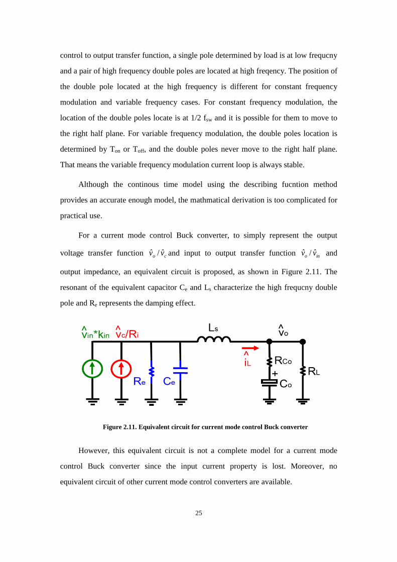
For a current mode control Buck converter, to simply represent the output
voltage transfer function co vv ˆ/ˆ and input to output transfer function ino vv ˆ/ˆ and
output impedance, an equivalent circuit is proposed, as shown in Figure 2.11. The
resonant of the equivalent capacitor Ce and Ls characterize the high frequcny double
pole and Re represents the damping effect.
Figure 2.11. Equivalent circuit for current mode control Buck converter
However, this equivalent circuit is not a complete model for a current mode
control Buck converter since the input current property is lost. Moreover, no
equivalent circuit of other current mode control converters are available.

26
2.3 Summary
In this chapter, the existing model for current mode control is reviewed. The
limitation of current source model, average models, discrete time model and modified
average model for current-mode control is identified. The continuous time model and
its equivalent circuit of Buck converter are introduced. The deficiency of the
equivalent circuit is discussed.
27
Chapter 3. Proposed Unified Three-terminal Switch
Mode for Current Mode Controls
This chapter introduces a new unified three-terminal switch mode for
current-mode controls. The proposed model takes the active switch, passive switch
and the closed current loop as an invariant entity, which is a common sub-circuit for
different topologies, and uses the three-terminal equivalent circuit to represent the
small signal behavior of this common sub-circuit in current mode control power
converter. The derivation process utilizes the small signal relationship between the
terminal voltage and the current, which are obtained from describing function method.
The proposed model is a unified model, which is applicable to constant frequency
peak current mode control, valley current mode control and charge control, and
variable frequency constant on-time control and constant off-time control. Small
signal model for commonly used topologies with current mode control can be easily
obtained by replacing the three-terminal switch with the current feedback loop, by the
three-terminal small signal equivalent circuit point by point.
3.1 Common Invariant Structure in Current Mode Control
Power Converters
28
Figure 3.1 Current mode control DC/DC converters
Current-mode control has unique advantages over voltage mode control, such as
fast dynamic response and inherent current limit. It is also an indispensable technique
to achieve current sharing and, AVP control. As a result, current mode control has
been widely used in the power converter design. The most commonly used power
converter topologies are Buck, Boost, Buck-boost, Flyback, forward and some other
topologies derived from these basic ones.
Basic current mode control power converters are shown in Figure 3.1. Although
topologies are different, they have basic structure in common. It consists of an active
switch, a passive switch, inductor and a closed current loop. The common node active
switch and passive switch connects to the inductor. The terminal designations a,p,c
refer to active, passive, and common respectively. vc is the control signal, which is the
output of the voltage loop compensator. The common three-terminal structure is
shown in Figure 3.2.
This three-terminal structure is an extension of the three-terminal switch of power
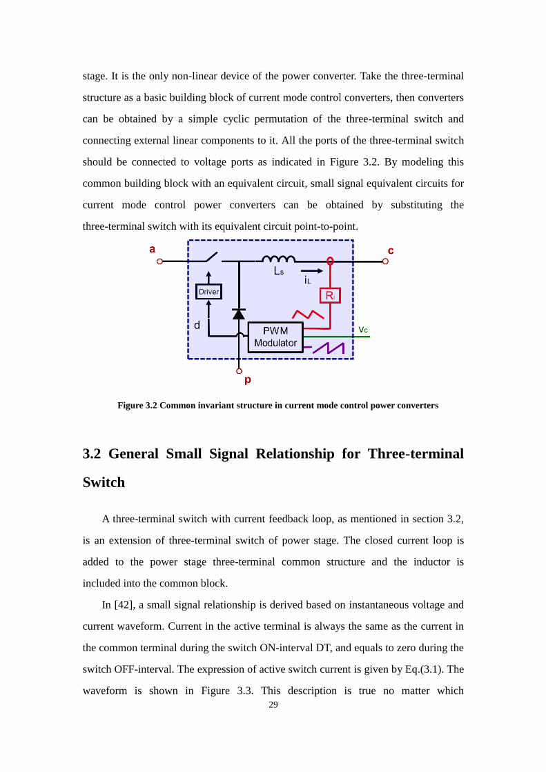
29
stage. It is the only non-linear device of the power converter. Take the three-terminal
structure as a basic building block of current mode control converters, then converters
can be obtained by a simple cyclic permutation of the three-terminal switch and
connecting external linear components to it. All the ports of the three-terminal switch
should be connected to voltage ports as indicated in Figure 3.2. By modeling this
common building block with an equivalent circuit, small signal equivalent circuits for
current mode control power converters can be obtained by substituting the
three-terminal switch with its equivalent circuit point-to-point.
Figure 3.2 Common invariant structure in current mode control power converters
3.2 General Small Signal Relationship for Three-terminal
Switch
A three-terminal switch with current feedback loop, as mentioned in section 3.2,
is an extension of three-terminal switch of power stage. The closed current loop is
added to the power stage three-terminal common structure and the inductor is
included into the common block.
In [42], a small signal relationship is derived based on instantaneous voltage and
current waveform. Current in the active terminal is always the same as the current in
the common terminal during the switch ON-interval DT, and equals to zero during the
switch OFF-interval. The expression of active switch current is given by Eq.(3.1). The
waveform is shown in Figure 3.3. This description is true no matter which
30
configuration the switch is implemented in.
ss
sc
aTtDT
DTttiti
,
),()(
0
0
(3.1)
Figure 3.3 Basic waveform of PWM switch
Using average concept, average terminal currents ia, and ic, we have from very
simple relations:
ca idi (3.2)
Perturb the Eq.(3.2) and neglect the high order term, a small signal relationship
between ia and ic is derived as Eq.(3.3).
cca IdiDi ˆˆˆ (3.3)
Essentially, the Eq. is an average model and it can be proved that is it accurate up
to 1/2 fsw. The instantaneous current relationship is given by Eq.(3.3) is valid as long
as the PWM power converter works in continuous current mode, regardless of the
implementation of the pulse-width modulator.
For the three-terminal switch under current mode control, since all the
assumption used in deriving Eq.(3.1) is not violated, the small signal given by Eq.(3.3)
is also true. This conclusion is verified by the Simplis simulation. Using peak current
31
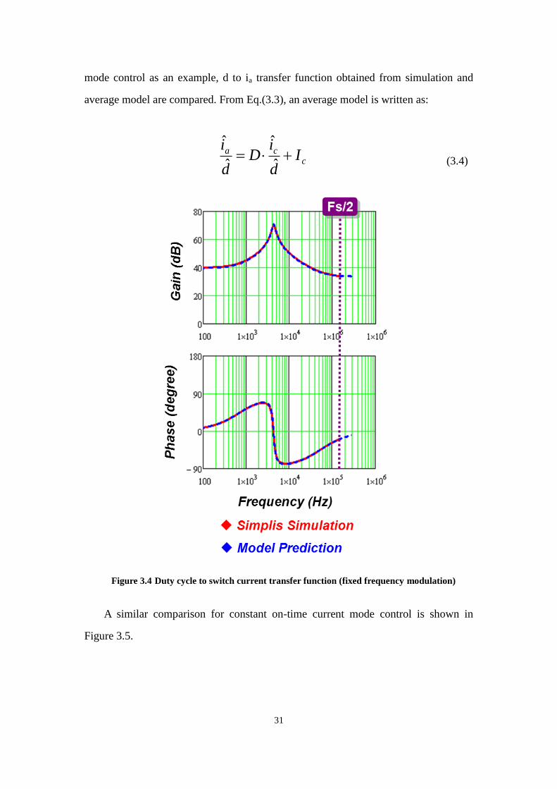
mode control as an example, d to ia transfer function obtained from simulation and
average model are compared. From Eq.(3.3), an average model is written as:
cca Id
iD
d
i
ˆ
ˆ
ˆ
ˆ
(3.4)
Figure 3.4 Duty cycle to switch current transfer function (fixed frequency modulation)
A similar comparison for constant on-time current mode control is shown in
Figure 3.5.
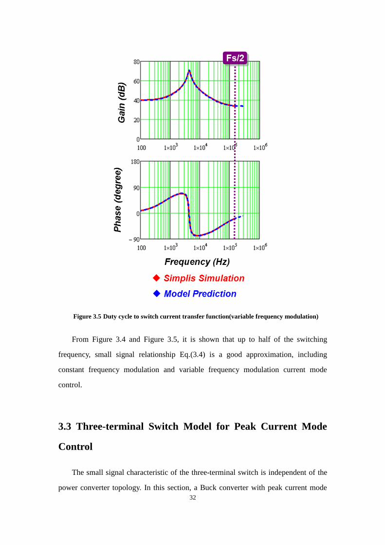
32
Figure 3.5 Duty cycle to switch current transfer function(variable frequency modulation)
From Figure 3.4 and Figure 3.5, it is shown that up to half of the switching
frequency, small signal relationship Eq.(3.4) is a good approximation, including
constant frequency modulation and variable frequency modulation current mode
control.
3.3 Three-terminal Switch Model for Peak Current Mode
Control
The small signal characteristic of the three-terminal switch is independent of the
power converter topology. In this section, a Buck converter with peak current mode
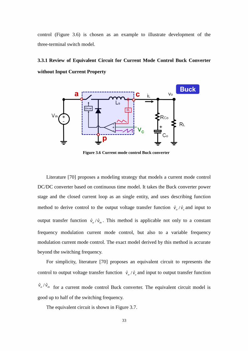
33
control (Figure 3.6) is chosen as an example to illustrate development of the
three-terminal switch model.
3.3.1 Review of Equivalent Circuit for Current Mode Control Buck Converter
without Input Current Property
Figure 3.6 Current mode control Buck converter
Literature [70] proposes a modeling strategy that models a current mode control
DC/DC converter based on continuous time model. It takes the Buck converter power
stage and the closed current loop as an single entity, and uses describing function
method to derive control to the output voltage transfer function co vv ˆ/ˆ and input to
output transfer function ino vv ˆ/ˆ . This method is applicable not only to a constant
frequency modulation current mode control, but also to a variable frequency
modulation current mode control. The exact model derived by this method is accurate
beyond the switching frequency.
For simplicity, literature [70] proposes an equivalent circuit to represents the
control to output voltage transfer function co vv ˆ/ˆ and input to output transfer function
ino vv ˆ/ˆ for a current mode control Buck converter. The equivalent circuit model is
good up to half of the switching frequency.
The equivalent circuit is shown in Figure 3.7.
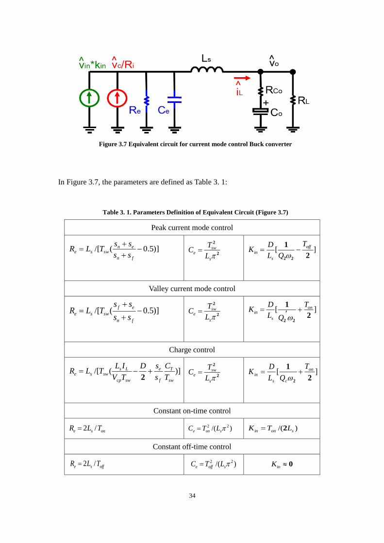
34
Figure 3.7 Equivalent circuit for current mode control Buck converter
In Figure 3.7, the parameters are defined as Table 3. 1:
Table 3. 1. Parameters Definition of Equivalent Circuit (Figure 3.7)
Peak current mode control
2
2
s
swe
L
TC ][
2
1
22
off
s
in
T
QL
DK
Valley current mode control
2
2
s
swe
L
TC ][
2
1
22
on
s
in
T
QL
DK
Charge control
2
2
s
swe
L
TC ][
2
1
2
on
cs
in
T
QL
DK
Constant on-time control
)/( sonin LTK 2
Constant off-time control
0inK
)]5.0(/[
fn
enswse
ss
ssTLR
)]5.0(/[
fn
ef
swsess
ssTLR
)](/[sw
T
f
e
swcp
Lsswse
T
C
s
sD
TV
ILTLR
2
onse TLR /2 )/( 22 sone LTC
offse TLR /2 )/( 22 soffe LTC
35
This equivalent circuit correctly represents the inductor current property under
control signal perturbation and input voltage and output voltage perturbation, but
switch current and diode current properties are lost.
To correctly represent the small signal behavior of the three-terminal structure
(Figure 3.2), the equivalent circuit should have three terminals corresponding to the
switch model. In such a three-terminal structure, if two terminal currents are correctly
represented, the accuracy of the third terminal current is guaranteed by Kirchhoff's
Current Law. Since the equivalent circuit in Figure 3.7 represents the inductor
property, it is a good starting point when building the three-terminal equivalent
circuit.
3.3.2 Complete Equivalent Circuit for Current Mode Control Buck Converter
The equivalent circuit Figure 3.7 accurately represents the property of the
common terminal current. The strategy of deriving a three-terminal equivalent circuit
is modifying the equivalent circuit in Figure 3.7, keeping the inductor current and
adding a proper part to represent the active switch current. The correctness of the
passive switch current property is guaranteed by Kirchhoff's Current Law.
The equivalent circuit is redrawn in Figure 3.8 with the introduction of a DC
transformer with turns ratio D, which is the steady state duty cycle. On the secondary
side, the inductor terminal is defined as c corresponding to the circuit diagram. On the
primary side, the terminal a and p are defined by the corresponding circuit diagram.
The inv̂ controlled current source
inin kv ˆ in Figure 3.7 is equivalently represented by
input voltage inv̂ together with an input voltage controlled voltage source apin Kv ˆ ,
where apK is defined as:
1
D
RKK ein
ap (3. 5)
Since Ce forms double poles with Ls at half the switching frequency, at low
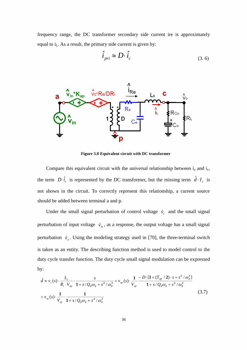
36
frequency range, the DC transformer secondary side current ire is approximately
equal to iL. As a result, the primary side current is given by:
cpri iDi ˆˆ
(3. 6)
Figure 3.8 Equivalent circuit with DC transformer
Compare this equivalent circuit with the universal relationship between ia and ic,
the term ciD ˆ is represented by the DC transformer, but the missing term cId ˆ is
not shown in the circuit. To correctly represent this relationship, a current source
should be added between terminal a and p.
Under the small signal perturbation of control voltage cv̂ and the small signal
perturbation of input voltage inv̂ , as a response, the output voltage has a small signal
perturbation ov̂ . Using the modeling strategy used in [70], the three-terminal switch
is taken as an entity. The describing function method is used to model control to the
duty cycle transfer function. The duty cycle small signal modulation can be expressed
by:
2
2
2
22
2
2
2
22
2
2
2
2
2
2
22
1
11
1
211
1
//)(
//
]/)/([)(
//)(ˆ
sQsVsv
sQs
ssTD
Vsv
sQs
s
VR
Lsvd
cp
cp
off
ap
ap
api
s
c
(3.7)
37
where
).(
,/
50
122
fn
en
sw
ss
ssQT
Based on Eq.(3.7), the cId ˆ term is expressed by:
2
2
2
22
2
2
2
22
2
2
2
2
2
2
22
1
1
1
21
1
//)(
//
]/)/([)(
//)(ˆ
sQsV
Isv
sQs
ssTD
V
Isv
sQs
s
VR
ILsvId
ap
ccp
off
ap
cap
api
cscc
(3.8)
In the small signal equivalent circuit Figure 3.8, under small signal perturbation
of control voltage cv̂ , and the small signal perturbation of input voltage apv̂ , the
output voltage small signal perturbation is cpv̂ . Then, the inductor voltage small
signal response Lv̂ can be easily obtained:
]//
[)(
]//
])/(/[)[(
//)(ˆ
11
1
1
21
1
2
2
2
22
2
2
2
22
22
2
2
2
22
sQssv
sQs
sDTQsv
sQs
s
R
Lsvv
cp
off
ap
i
s
cL
(3.9)
When compare Eq.(3.8) and Eq.(3.9), it is found that they have similar dynamic
terms. So, the equation for cId ˆ can be rearranged and expressed by Lv̂ in a simple
way:
apapcpcpLL
c
ap
ap
ap
c
cpcp
off
ap
i
s
c
ap
c
c
RvGvGv
ID
Vsv
V
Isv
sQssv
sQs
sDTQsv
sQs
s
R
Lsv
V
IId
/ˆˆˆ
)/()()(]}//
[)(
//
])/(/[)(
//)({ˆ
11
1
1
21
1
2
2
2
22
2
2
2
22
22
2
2
2
22
where c
ap
ap
ap
c
cpLDI
VR
V
IGG ,
(3.10)
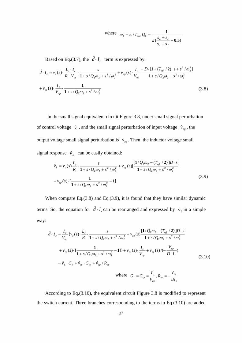
According to Eq.(3.10), the equivalent circuit Figure 3.8 is modified to represent
the switch current. Three branches corresponding to the terms in Eq.(3.10) are added
38
between terminal a and terminal p. The complete equivalent circuit for the peak
current mode control Buck converter is Figure 3.9.
Figure 3.9 Complete equivalent circuit for peak current mode control Buck converter
3.3.3 Three-terminal Switch Mode for Peak Current Mode Control
Comparing the circuit diagram with the small signal equivalent circuit, the linear
part in the circuit is kept the same as in the equivalent circuit, and the common
three-terminal structure is replaced by a three-terminal equivalent circuit. Since the
previous derivation is independent of topology, this three-terminal equivalent circuit
is the small signal equivalent circuit for the common structure. The three terminal
equivalent circuit model for the peak current mode control is shown in Figure 3.10.
Figure 3.10 Three terminal equivalent circuit model for peak current mode
control
39
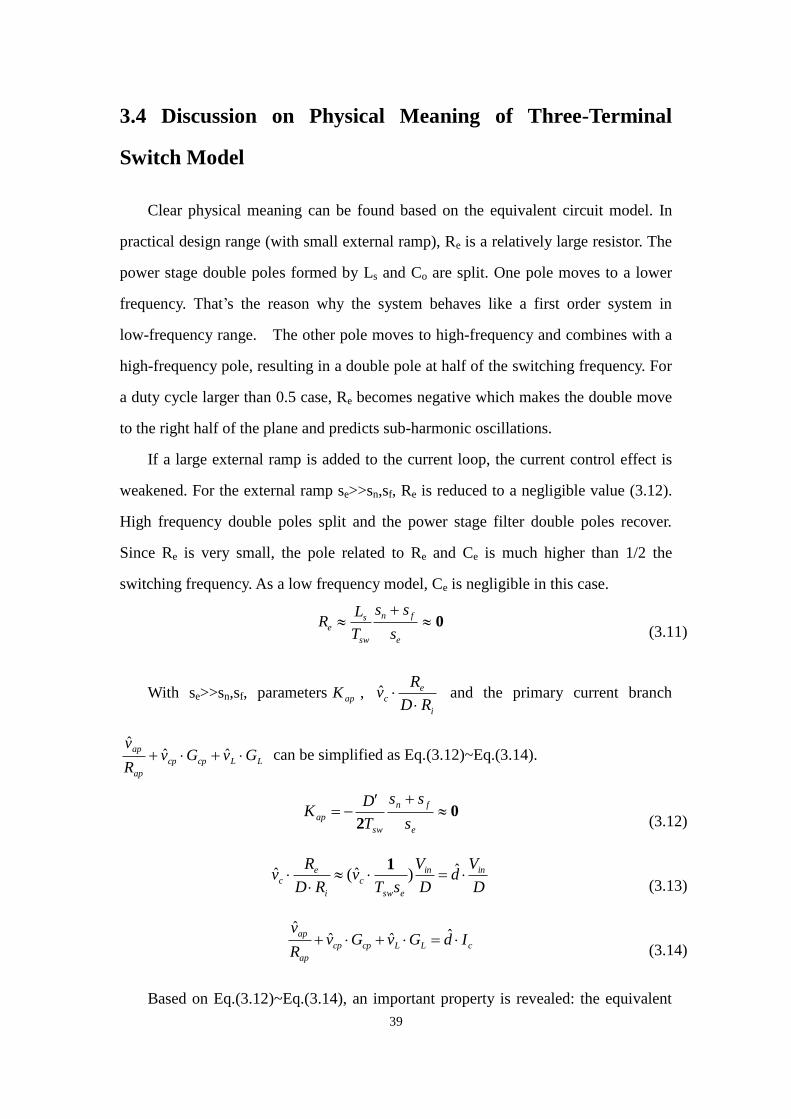
3.4 Discussion on Physical Meaning of Three-Terminal
Switch Model
Clear physical meaning can be found based on the equivalent circuit model. In
practical design range (with small external ramp), Re is a relatively large resistor. The
power stage double poles formed by Ls and Co are split. One pole moves to a lower
frequency. That’s the reason why the system behaves like a first order system in
low-frequency range. The other pole moves to high-frequency and combines with a
high-frequency pole, resulting in a double pole at half of the switching frequency. For
a duty cycle larger than 0.5 case, Re becomes negative which makes the double move
to the right half of the plane and predicts sub-harmonic oscillations.
If a large external ramp is added to the current loop, the current control effect is
weakened. For the external ramp se>>sn,sf, Re is reduced to a negligible value (3.12).
High frequency double poles split and the power stage filter double poles recover.
Since Re is very small, the pole related to Re and Ce is much higher than 1/2 the
switching frequency. As a low frequency model, Ce is negligible in this case.
0
e
fn
sw
se
s
ss
T
LR
(3.11)
With se>>sn,sf, parameters apK , i
ec
RD
Rv
ˆ and the primary current branch
LLcpcp
ap
apGvGv
R
v ˆˆ
ˆ can be simplified as Eq.(3.12)~Eq.(3.14).
02
e
fn
sw
aps
ss
T
DK
(3.12)
D
Vd
D
V
sTv
RD
Rv inin
esw
c
i
ec
ˆ)ˆ(ˆ
1
(3.13)
cLLcpcp
ap
apIdGvGv
R
v ˆˆˆ
ˆ
(3.14)
Based on Eq.(3.12)~Eq.(3.14), an important property is revealed: the equivalent
40
circuit is a unified model showing the unification of the current mode control and
voltage control. With the external ramp increase, the current control effect is
weakened. If se>>sn,sf, current feedback information is negligible, the three-terminal
switch mode for current mode control degenerates to a three-terminal switch mode for
the power stage [42], as shown in Figure 3.11.
Figure 3.11 Three terminal equivalent circuit model degenerates to
three-terminal switch mode for the power stage when se>>sn,sf
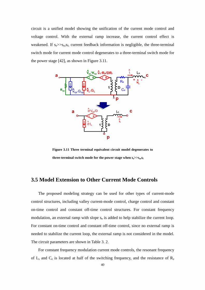
3.5 Model Extension to Other Current Mode Controls
The proposed modeling strategy can be used for other types of current-mode
control structures, including valley current-mode control, charge control and constant
on-time control and constant off-time control structures. For constant frequency
modulation, an external ramp with slope se is added to help stabilize the current loop.
For constant on-time control and constant off-time control, since no external ramp is
needed to stabilize the current loop, the external ramp is not considered in the model.
The circuit parameters are shown in Table 3. 2.
For constant frequency modulation current mode controls, the resonant frequency
of Ls and Ce is located at half of the switching frequency, and the resistance of Re
41
could be positive or negative, depending on the duty cycle and load current. Negative
Re indicates that the current loop is unstable, suffer to sub-harmonic oscillation. Using
an external ramp can help to stabilize the current loop and achieve a proper damping
of the double poles at half of the switching frequency.
For variable frequency modulation current mode control, the resonant frequency
of Ls and Ce is located at a certain frequency higher than half of the switching
frequency, which is determined by Ton or Toff, and the resistance of Re is always
positive. This circuit can be used to illustrate the instability of the current loop. The
key transfer functions, including the control-to-output transfer function, the audio
susceptibility, and the input impedance and output impedance, can be easily
calculated based on the equivalent model.
Figure 3.12 Unified three terminal equivalent circuit model for current
mode controls
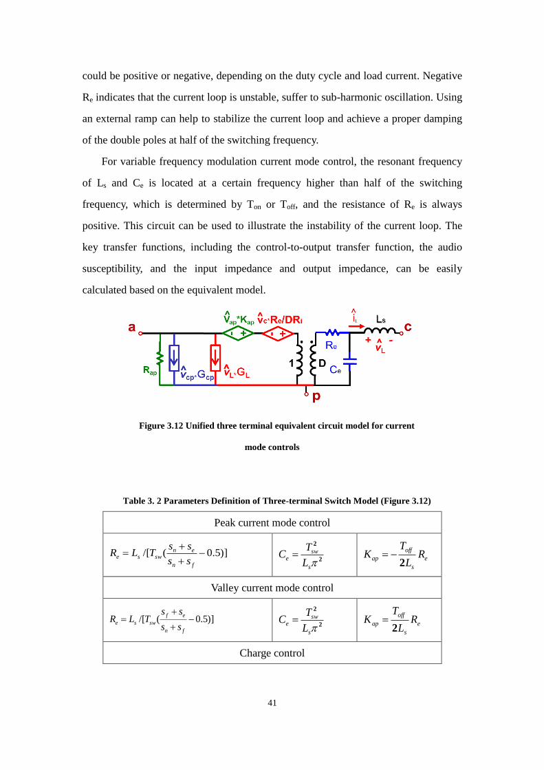
Table 3. 2 Parameters Definition of Three-terminal Switch Model (Figure 3.12)
Peak current mode control
2
2
s
swe
L
TC e
s
off
ap RL
TK
2
Valley current mode control
2
2
s
swe
L
TC e
s
off
ap RL
TK
2
Charge control
)]5.0(/[
fn
enswse
ss
ssTLR
)]5.0(/[
fn
ef
swsess
ssTLR
42
2
2
s
swe
L
TC e
s
onap R
L
TK
2
Constant on-time control
onoffap TTK /
Constant off-time control
1apK
3.6 Simulation Verification of the Proposed Model
The proposed small signal model is verified in this section. The SIMPLIS
simulation tool is used to verify the proposed model.
3.6.1 Constant Frequency Modulation Current Mode Control
A. Peak current mode control Buck converter
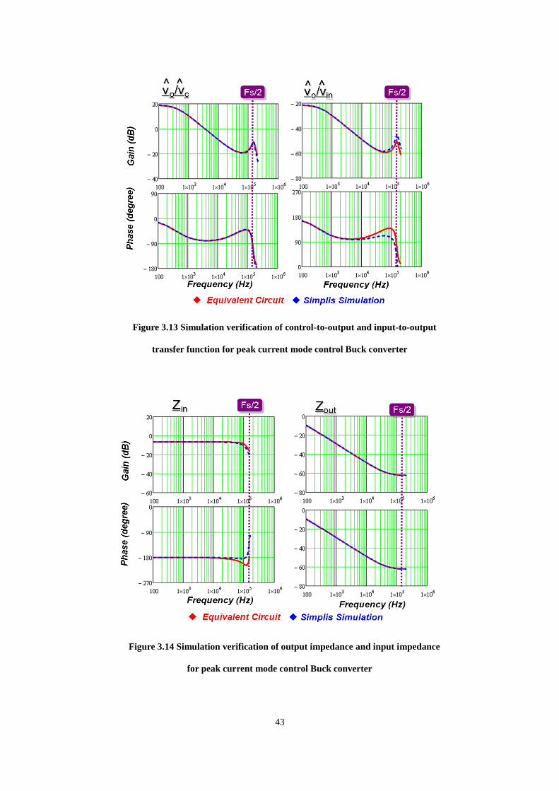
The parameters of the peak current-mode control buck converter are as follows:
Vin = 12V, Vo = 5V, fs = 300KHz, Co = 8×560μF, RCo = 6/8mΩ, and Ls =300nH. The
control-to-output transfer function and the audio susceptibility are shown in Figure
3.13 while input and output impedance comparisons are shown and Figure 3.14. The
proposed model can accurately predict the system response up to half of the switching
frequency.
)](/[sw
T
f
e
swcp
Lsswse
T
C
s
sD
TV
ILTLR
2
onse TLR /2 )/( 22 sone LTC
offse TLR /2 )/( 22 soffe LTC
43
Figure 3.13 Simulation verification of control-to-output and input-to-output
transfer function for peak current mode control Buck converter
Figure 3.14 Simulation verification of output impedance and input impedance
for peak current mode control Buck converter
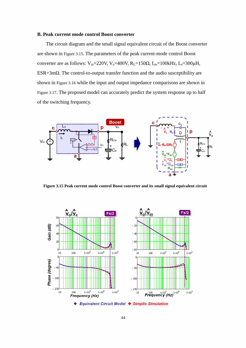
44
B. Peak current mode control Boost converter
The circuit diagram and the small signal equivalent circuit of the Boost converter
are shown in Figure 3.15. The parameters of the peak current-mode control Boost
converter are as follows: Vin=220V, Vo=400V, RL=150Ω, fsw=100kHz, Ls=300μH,
ESR=3mΩ. The control-to-output transfer function and the audio susceptibility are
shown in Figure 3.16 while the input and output impedance comparisons are shown in
Figure 3.17. The proposed model can accurately predict the system response up to half
of the switching frequency.
Figure 3.15 Peak current mode control Boost converter and its small signal equivalent circuit
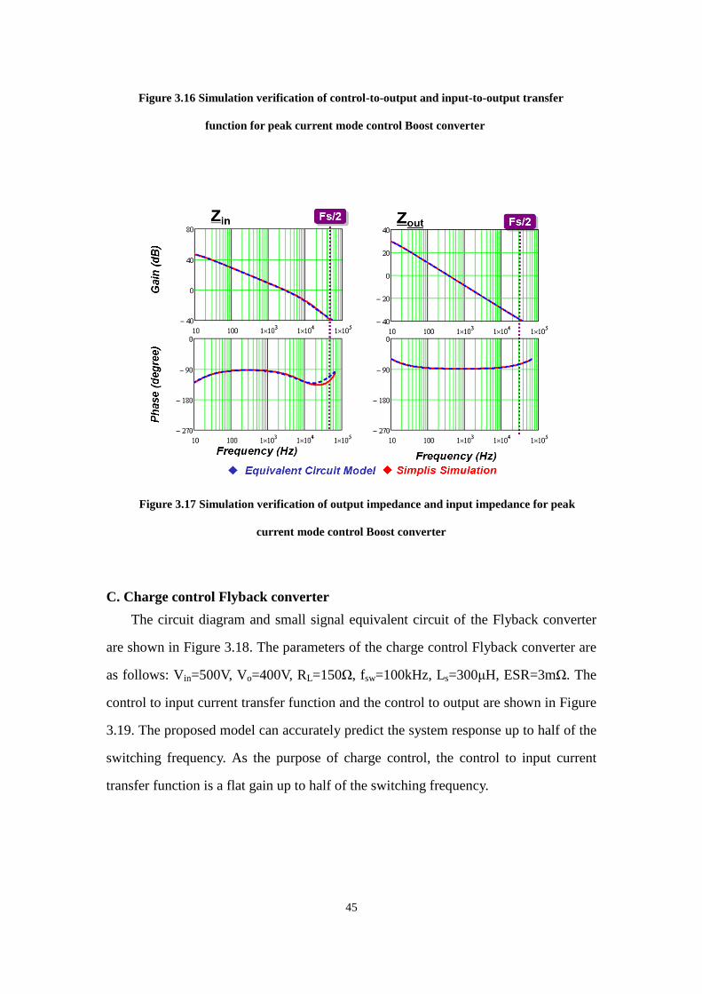
45
Figure 3.16 Simulation verification of control-to-output and input-to-output transfer
function for peak current mode control Boost converter
Figure 3.17 Simulation verification of output impedance and input impedance for peak
current mode control Boost converter
C. Charge control Flyback converter
The circuit diagram and small signal equivalent circuit of the Flyback converter
are shown in Figure 3.18. The parameters of the charge control Flyback converter are
as follows: Vin=500V, Vo=400V, RL=150Ω, fsw=100kHz, Ls=300μH, ESR=3mΩ. The
control to input current transfer function and the control to output are shown in Figure
3.19. The proposed model can accurately predict the system response up to half of the
switching frequency. As the purpose of charge control, the control to input current
transfer function is a flat gain up to half of the switching frequency.
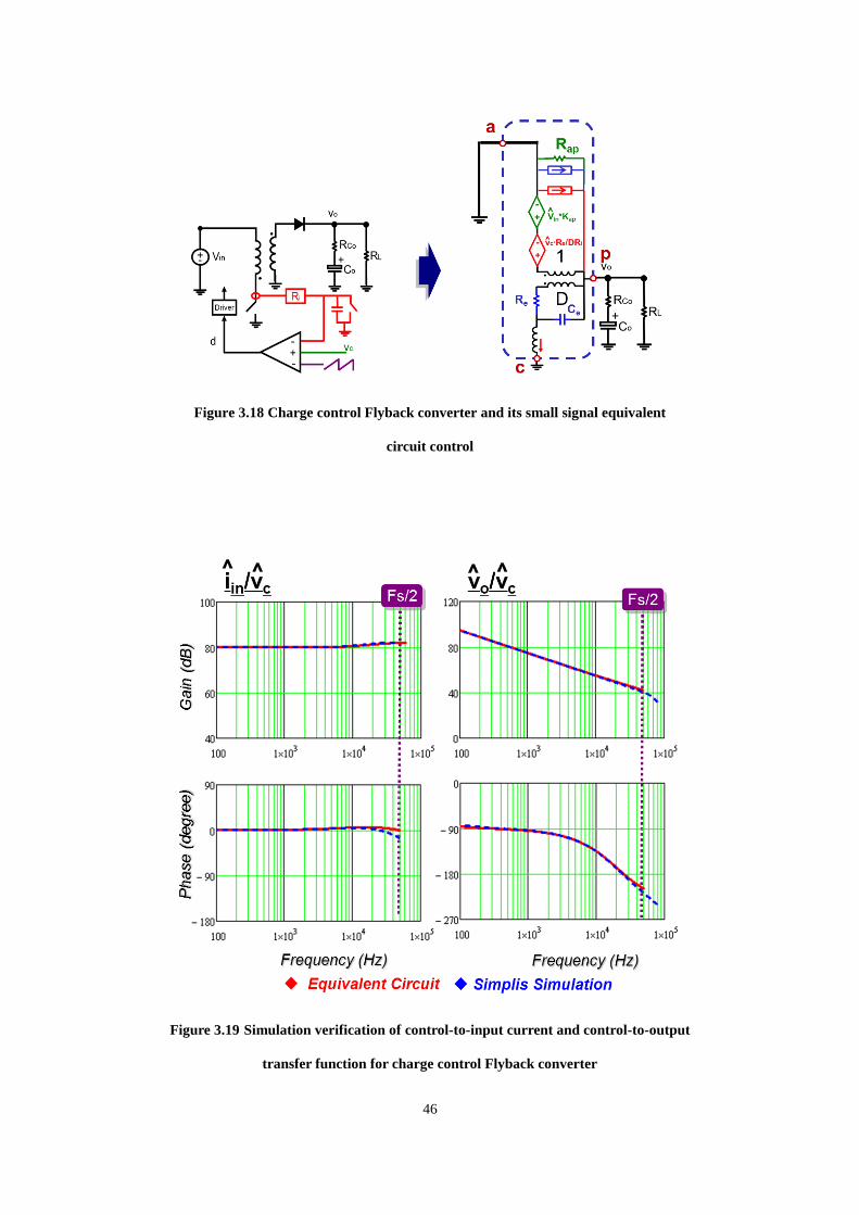
46
Figure 3.18 Charge control Flyback converter and its small signal equivalent
circuit control
Figure 3.19 Simulation verification of control-to-input current and control-to-output
transfer function for charge control Flyback converter
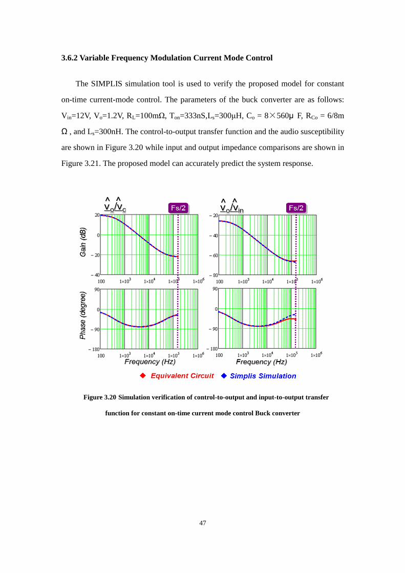
47
3.6.2 Variable Frequency Modulation Current Mode Control
The SIMPLIS simulation tool is used to verify the proposed model for constant
on-time current-mode control. The parameters of the buck converter are as follows:
Vin=12V, Vo=1.2V, RL=100mΩ, Ton=333nS,Ls=300μH, Co = 8×560μ F, RCo = 6/8m
Ω , and Ls=300nH. The control-to-output transfer function and the audio susceptibility
are shown in Figure 3.20 while input and output impedance comparisons are shown in
Figure 3.21. The proposed model can accurately predict the system response.
Figure 3.20 Simulation verification of control-to-output and input-to-output transfer
function for constant on-time current mode control Buck converter
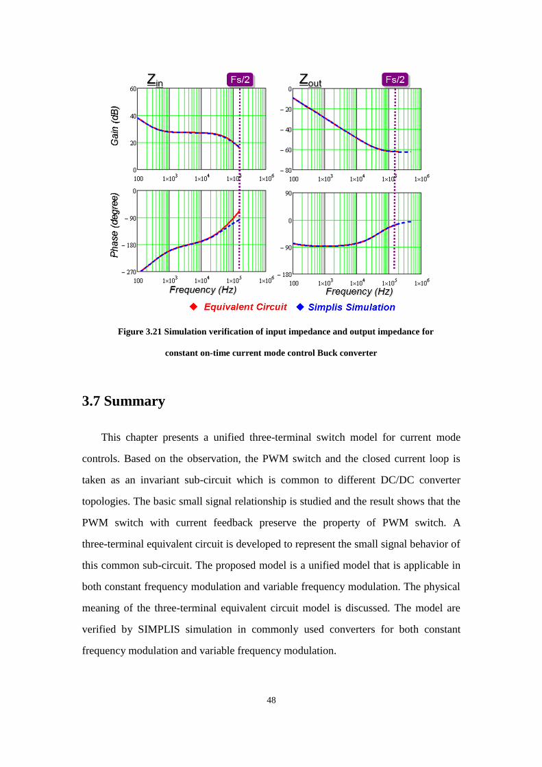
48
Figure 3.21 Simulation verification of input impedance and output impedance for
constant on-time current mode control Buck converter
3.7 Summary
This chapter presents a unified three-terminal switch model for current mode
controls. Based on the observation, the PWM switch and the closed current loop is
taken as an invariant sub-circuit which is common to different DC/DC converter
topologies. The basic small signal relationship is studied and the result shows that the
PWM switch with current feedback preserve the property of PWM switch. A
three-terminal equivalent circuit is developed to represent the small signal behavior of
this common sub-circuit. The proposed model is a unified model that is applicable in
both constant frequency modulation and variable frequency modulation. The physical
meaning of the three-terminal equivalent circuit model is discussed. The model are
verified by SIMPLIS simulation in commonly used converters for both constant
frequency modulation and variable frequency modulation.
49
Chapter 4. Comparison of Current Mode Controls
with Different Implementation Based on Proposed
Model
In this section, based on the small signal model obtained in chapter 3, a
comparison of current mode controls with different implementation is discussed.
According to application requirement and operating condition, different
implementations exhibit their own unique advantage. The application of charge
control is mainly on the application needed to control input current. The discussion
compares peak current mode control, valley current mode control, constant on-time
control and constant off-time control implementation, which are most commonly used
in DC/DC converter design[29][72][73][74][75].
The discussion is based on a current mode control Buck converter with different
implementation.
4.1 Control-to-output Transfer Function and Voltage Loop
Design
Based on the equivalent circuit model, control-to-output transfer function of all
the current mode control can be expressed by a unified form:
2
2
1
1
1
1
xxx
a
oCo
c
c
o
s
Q
ss
sCRK
sv
sv
/
)(
)(ˆ
)(ˆ
(4.1)
With different implementation, low frequency pole are similar: the position is
determined by the load resistor and output capacitor.
High frequency double poles are fundamentally different:
For constant frequency modulation current mode control, the double poles are
half of the switching frequency:
50
swswx ff 22
1
(4.2)
Proper design of the external ramp can guarantee the quality factor around 1. For
peak current mode control, for D>0.5 case, an external ramp is necessary to stabilize
the current loop. In contrast, for valley current mode control, external ramp is
necessary for D<0.5 application.
For constant on-time control, the double poles locations are determined by
on-time:
on
xT
(4.3)
The double poles quality factor is a constant value:
2xQ
(4.4)
For constant off-time control, the double poles locations are determined by
Off-time:
off
xT
(4.5)
The double poles quality factor is also a constant value:
2xQ
(4.6)
This characteristic is the basis of selecting the implementation of current mode
control.
For a small duty cycle application, such as voltage regulator for microprocessor
[20], the duty ration is only around 0.1 so peak current mode control does not need an
external ramp to achieve a proper double pole damping while it is necessary for valley
current mode control. It is obvious that peak current mode control is simpler to
implement. Based on Eq.(4.3)(4.5), the double poles of constant on-time control are
around 5 times of the switching frequency, while those of constant off-time control
are around half the switching frequency. The pole-zero-map Figure 4.1 clearly shows
the difference between them.
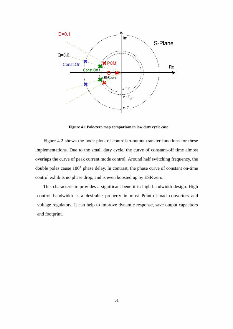
51
Figure 4.1 Pole-zero map comparison in low duty cycle case
Figure 4.2 shows the bode plots of control-to-output transfer functions for these
implementations. Due to the small duty cycle, the curve of constant-off time almost
overlaps the curve of peak current mode control. Around half switching frequency, the
double poles cause 180° phase delay. In contrast, the phase curve of constant on-time
control exhibits no phase drop, and is even boosted up by ESR zero.
This characteristic provides a significant benefit in high bandwidth design. High
control bandwidth is a desirable property in most Point-of-load converters and
voltage regulators. It can help to improve dynamic response, save output capacitors
and footprint.
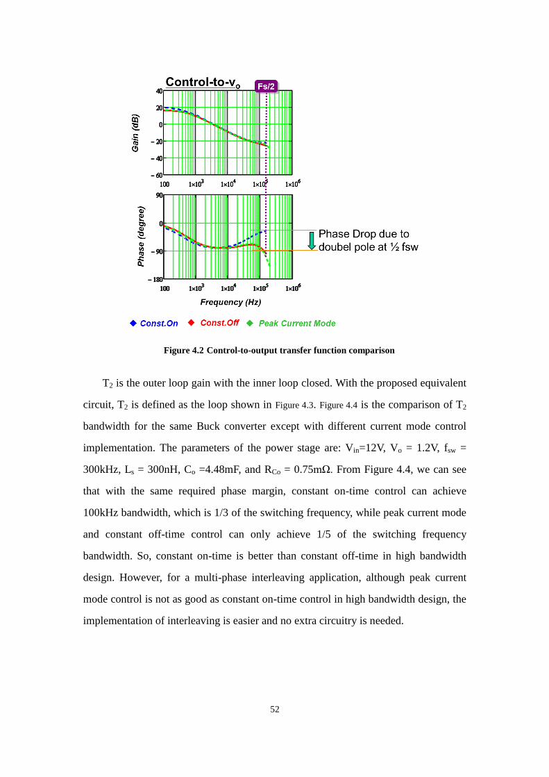
52
Figure 4.2 Control-to-output transfer function comparison
T2 is the outer loop gain with the inner loop closed. With the proposed equivalent
circuit, T2 is defined as the loop shown in Figure 4.3. Figure 4.4 is the comparison of T2
bandwidth for the same Buck converter except with different current mode control
implementation. The parameters of the power stage are: Vin=12V, Vo = 1.2V, fsw =
300kHz, Ls = 300nH, Co =4.48mF, and RCo = 0.75mΩ. From Figure 4.4, we can see
that with the same required phase margin, constant on-time control can achieve
100kHz bandwidth, which is 1/3 of the switching frequency, while peak current mode
and constant off-time control can only achieve 1/5 of the switching frequency
bandwidth. So, constant on-time is better than constant off-time in high bandwidth
design. However, for a multi-phase interleaving application, although peak current
mode control is not as good as constant on-time control in high bandwidth design, the
implementation of interleaving is easier and no extra circuitry is needed.
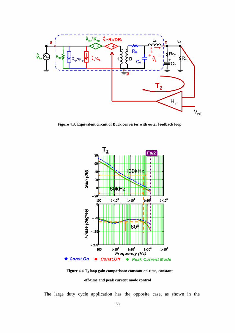
53
Figure 4.3. Equivalent circuit of Buck converter with outer feedback loop
Figure 4.4 T2 loop gain comparison: constant on-time, constant
off-time and peak current mode control
The large duty cycle application has the opposite case, as shown in the
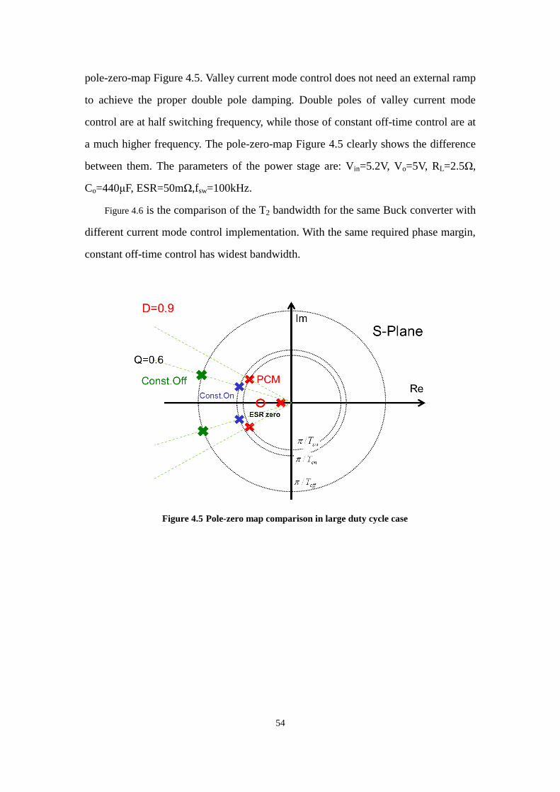
54
pole-zero-map Figure 4.5. Valley current mode control does not need an external ramp
to achieve the proper double pole damping. Double poles of valley current mode
control are at half switching frequency, while those of constant off-time control are at
a much higher frequency. The pole-zero-map Figure 4.5 clearly shows the difference
between them. The parameters of the power stage are: Vin=5.2V, Vo=5V, RL=2.5Ω,
Co=440μF, ESR=50mΩ,fsw=100kHz.
Figure 4.6 is the comparison of the T2 bandwidth for the same Buck converter with
different current mode control implementation. With the same required phase margin,
constant off-time control has widest bandwidth.
Figure 4.5 Pole-zero map comparison in large duty cycle case
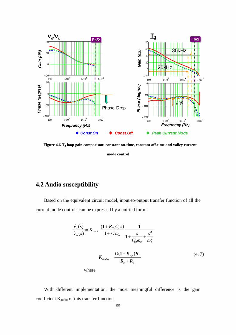
55
Figure 4.6 T2 loop gain comparison: constant on-time, constant off-time and valley current
mode control
4.2 Audio susceptibility
Based on the equivalent circuit model, input-to-output transfer function of all the
current mode controls can be expressed by a unified form:
2
2
2
22
1
1
1
1
s
Q
ss
sCRK
sv
sv
a
oCoaudio
in
o
/
)(
)(ˆ
)(ˆ
where
Le
Lap
audioRR
RKDK
)(1
(4. 7)
With different implementation, the most meaningful difference is the gain
coefficient Kaudio of this transfer function.
56
For different implementations of the current mode control, as mentioned in Table
3. 2, Kap is defined as:
Peak Current Mode Control:
e
s
off
ap RL
TK
2 (4. 8)
Valley Current Mode Control:
e
s
onap R
L
TK
2 (4. 9)
Constant on-time Current Mode Control:
on
off
apT
TK (4. 10)
Constant off-time Current Mode Control:
1apK (4. 11)
It is easy to simplify the expression of Kaudio for different current mode control:
Peak Current Mode Control:
Le
Laudio
RR
RQDDK
)/( 21 2 (4. 12)
Valley Current Mode Control:
Le
Laudio
RR
RQDDK
)/( 122 (4. 13)
Constant on-time Current Mode Control:
Le
Laudio
RR
RK
(4. 14)
Constant off-time Current Mode Control:
0audioK (4. 15)
Among these implementations, the gain Kaudio of valley current mode control and
57
constant on-time control is always positive, so it is impossible to achieve zero audio
susceptibility.
For peak current mode control, to make Kaudio=0, the external ramp should be:
fe ss 50. (4. 16)
However, this design criteria contradicts with the criteria of damping the control
to output transfer function’s high frequency double poles. To achieve proper damping,
namely, quality factor of the double poles equals to 1, the external ramp should be:
nfe sss 180820 .. (4. 17)
These two criteria are compatible with each other only in the case where duty
cycle D is around 0.2 to 0.4. As a result, with peak current mode control
implementation, null audio susceptibility is not achievable for all operating duty
cycle.
For constant off-time current mode control, since Kaudio=0 as an inherent property,
without external ramp design concern, it is the best current mode control
implementation if low audio susceptibility is a tight requirement in some designs.
This property is provided by the unique “feed-forward effect” of constant off-time
current mode control. As an inherent effect of the current loop, Kap=-1 is a pure gain,
so it can immediately respond to the input variation and cancel the impact of it.
Figure 4.7 shows a time domain simulation waveform. Under a line frequency
perturbation, the feed-forward effect modulates the duty cycle proportionally without
any delay. As a result, the output voltage is not influenced by the input voltage even
without voltage feedback. This is a significant benefit of constant off-time current
mode control for the application requiring fast input transient response.
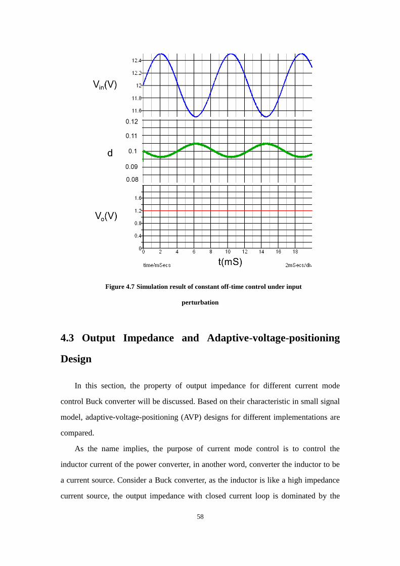
58
Figure 4.7 Simulation result of constant off-time control under input
perturbation
4.3 Output Impedance and Adaptive-voltage-positioning
Design
In this section, the property of output impedance for different current mode
control Buck converter will be discussed. Based on their characteristic in small signal
model, adaptive-voltage-positioning (AVP) designs for different implementations are
compared.
As the name implies, the purpose of current mode control is to control the
inductor current of the power converter, in another word, converter the inductor to be
a current source. Consider a Buck converter, as the inductor is like a high impedance
current source, the output impedance with closed current loop is dominated by the
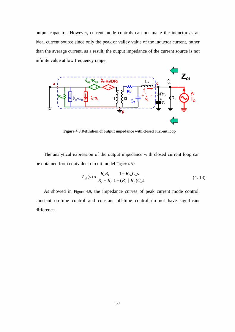
59
output capacitor. However, current mode controls can not make the inductor as an
ideal current source since only the peak or valley value of the inductor current, rather
than the average current, as a result, the output impedance of the current source is not
infinite value at low frequency range.
Figure 4.8 Definition of output impedance with closed current loop
The analytical expression of the output impedance with closed current loop can
be obtained from equivalent circuit model Figure 4.8 :
sCRR
sCR
RR
RRsZ
oLe
oCo
Le
Leoi
)||()(
1
1 (4. 18)
As showed in Figure 4.9, the impedance curves of peak current mode control,
constant on-time control and constant off-time control do not have significant
difference.
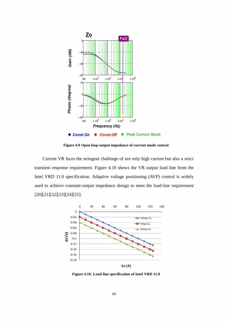
60
Figure 4.9 Open loop output impedance of current mode control
Current VR faces the stringent challenge of not only high current but also a strict
transient response requirement. Figure 4.10 shows the VR output load line from the
Intel VRD 11.0 specification. Adaptive voltage positioning (AVP) control is widely
used to achieve constant-output impedance design to meet the load-line requirement
[20][21][22][23][24][25].
Figure 4.10. Load-line specification of Intel VRD 11.0
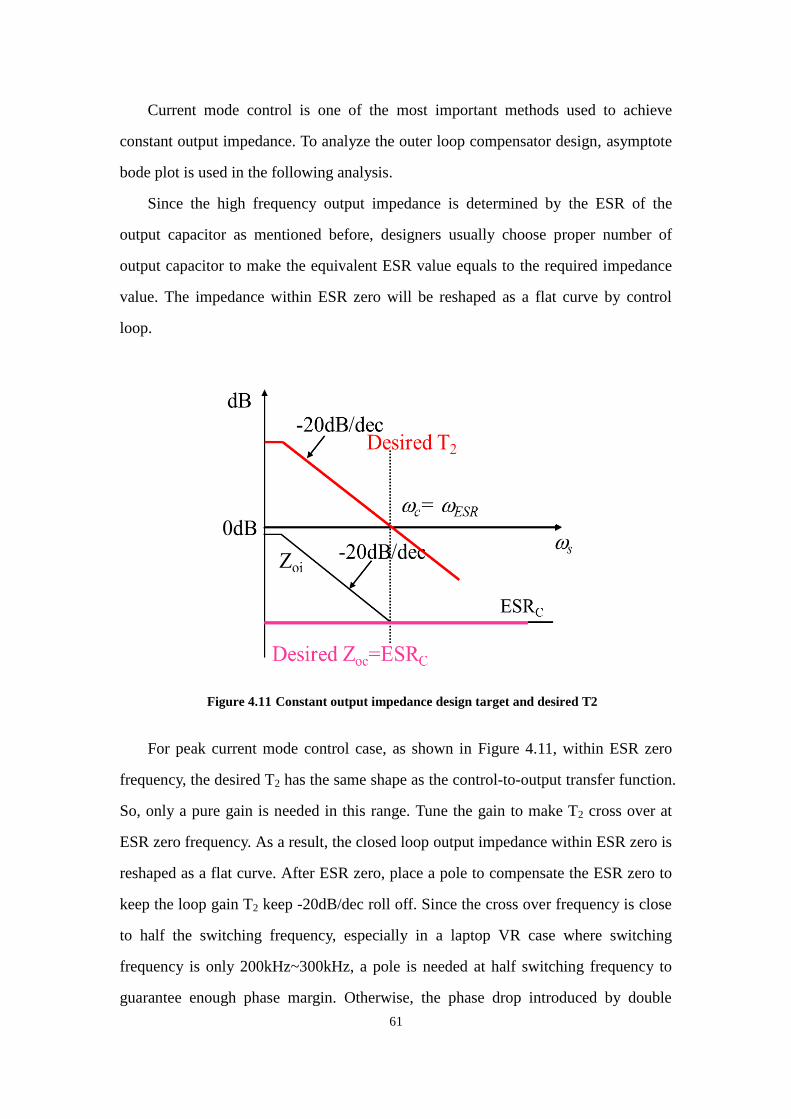
61
Current mode control is one of the most important methods used to achieve
constant output impedance. To analyze the outer loop compensator design, asymptote
bode plot is used in the following analysis.
Since the high frequency output impedance is determined by the ESR of the
output capacitor as mentioned before, designers usually choose proper number of
output capacitor to make the equivalent ESR value equals to the required impedance
value. The impedance within ESR zero will be reshaped as a flat curve by control
loop.
Figure 4.11 Constant output impedance design target and desired T2
For peak current mode control case, as shown in Figure 4.11, within ESR zero
frequency, the desired T2 has the same shape as the control-to-output transfer function.
So, only a pure gain is needed in this range. Tune the gain to make T2 cross over at
ESR zero frequency. As a result, the closed loop output impedance within ESR zero is
reshaped as a flat curve. After ESR zero, place a pole to compensate the ESR zero to
keep the loop gain T2 keep -20dB/dec roll off. Since the cross over frequency is close
to half the switching frequency, especially in a laptop VR case where switching
frequency is only 200kHz~300kHz, a pole is needed at half switching frequency to
guarantee enough phase margin. Otherwise, the phase drop introduced by double
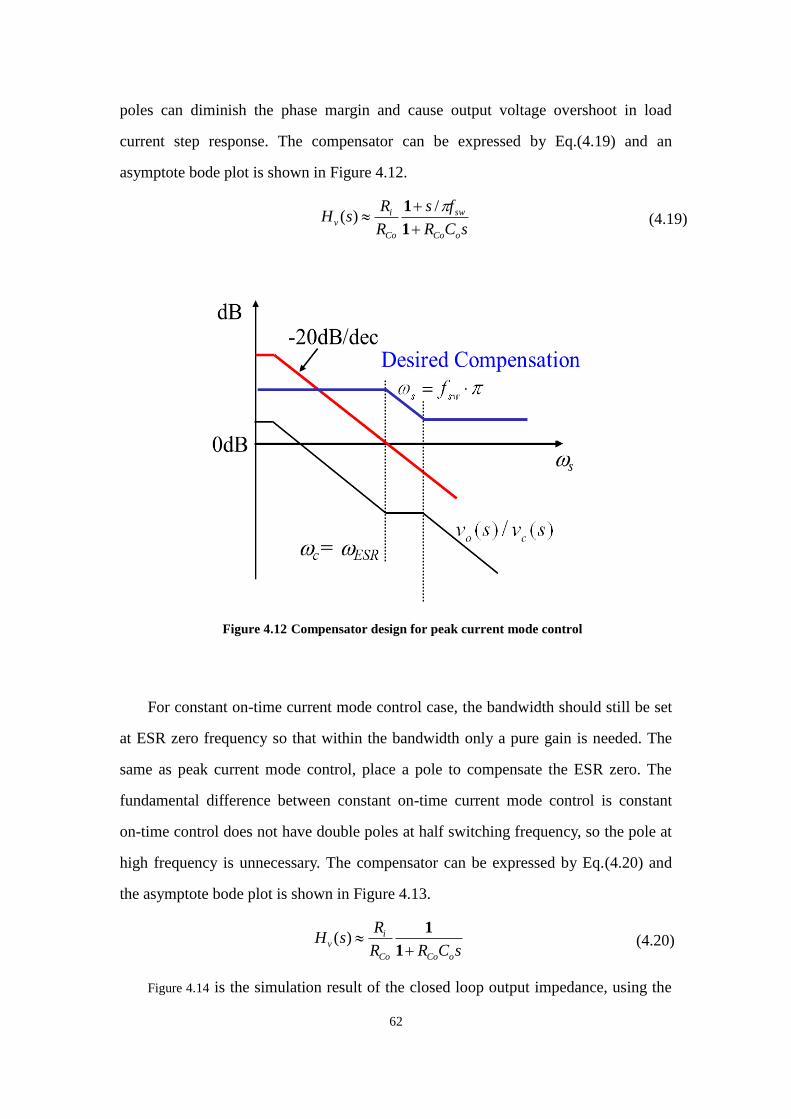
62
poles can diminish the phase margin and cause output voltage overshoot in load
current step response. The compensator can be expressed by Eq.(4.19) and an
asymptote bode plot is shown in Figure 4.12.
sCR
fs
R
RsH
oCo
sw
Co
iv
1
1 /)( (4.19)
Figure 4.12 Compensator design for peak current mode control
For constant on-time current mode control case, the bandwidth should still be set
at ESR zero frequency so that within the bandwidth only a pure gain is needed. The
same as peak current mode control, place a pole to compensate the ESR zero. The
fundamental difference between constant on-time current mode control is constant
on-time control does not have double poles at half switching frequency, so the pole at
high frequency is unnecessary. The compensator can be expressed by Eq.(4.20) and
the asymptote bode plot is shown in Figure 4.13.
sCRR
RsH
oCoCo
iv
1
1)( (4.20)
Figure 4.14 is the simulation result of the closed loop output impedance, using the
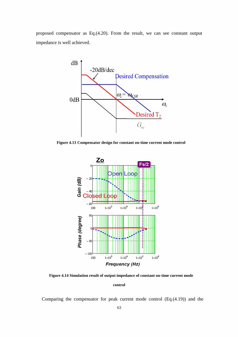
63
proposed compensator as Eq.(4.20). From the result, we can see constant output
impedance is well achieved.
Figure 4.13 Compensator design for constant on-time current mode control
Figure 4.14 Simulation result of output impedance of constant on-time current mode
control
Comparing the compensator for peak current mode control (Eq.(4.19)) and the
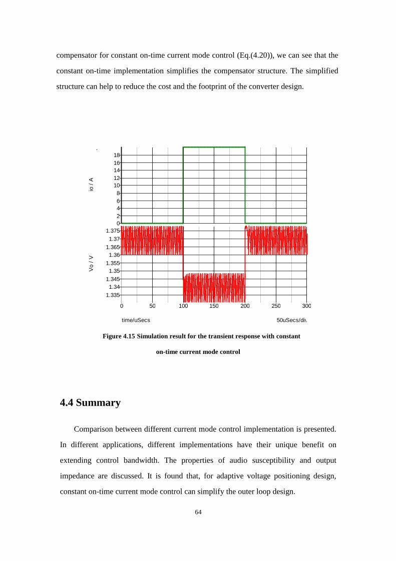
64
compensator for constant on-time current mode control (Eq.(4.20)), we can see that the
constant on-time implementation simplifies the compensator structure. The simplified
structure can help to reduce the cost and the footprint of the converter design.
Figure 4.15 Simulation result for the transient response with constant
on-time current mode control
4.4 Summary
Comparison between different current mode control implementation is presented.
In different applications, different implementations have their unique benefit on
extending control bandwidth. The properties of audio susceptibility and output
impedance are discussed. It is found that, for adaptive voltage positioning design,
constant on-time current mode control can simplify the outer loop design.
io /
A
0
2
4
6
8
10
12
14
16
18
time/uSecs 50uSecs/div
0 50 100 150 200 250 300
Vo /
V
1.335
1.34
1.345
1.35
1.355
1.36
1.365
1.37
1.375
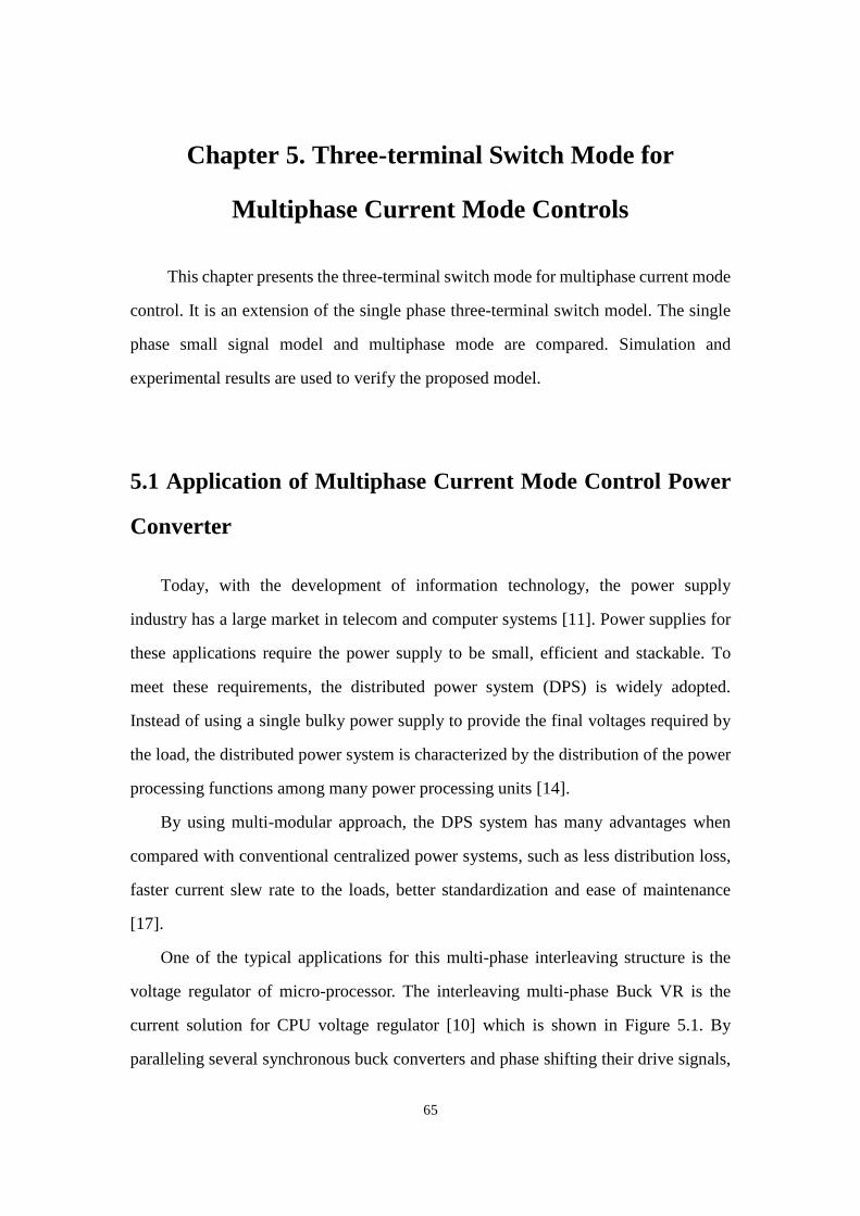
65
Chapter 5. Three-terminal Switch Mode for
Multiphase Current Mode Controls
This chapter presents the three-terminal switch mode for multiphase current mode
control. It is an extension of the single phase three-terminal switch model. The single
phase small signal model and multiphase mode are compared. Simulation and
experimental results are used to verify the proposed model.
5.1 Application of Multiphase Current Mode Control Power
Converter
Today, with the development of information technology, the power supply
industry has a large market in telecom and computer systems [11]. Power supplies for
these applications require the power supply to be small, efficient and stackable. To
meet these requirements, the distributed power system (DPS) is widely adopted.
Instead of using a single bulky power supply to provide the final voltages required by
the load, the distributed power system is characterized by the distribution of the power
processing functions among many power processing units [14].
By using multi-modular approach, the DPS system has many advantages when
compared with conventional centralized power systems, such as less distribution loss,
faster current slew rate to the loads, better standardization and ease of maintenance
[17].
One of the typical applications for this multi-phase interleaving structure is the
voltage regulator of micro-processor. The interleaving multi-phase Buck VR is the
current solution for CPU voltage regulator [10] which is shown in Figure 5.1. By
paralleling several synchronous buck converters and phase shifting their drive signals,
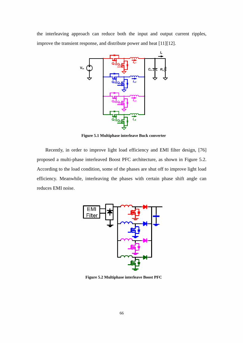
66
the interleaving approach can reduce both the input and output current ripples,
improve the transient response, and distribute power and heat [11][12].
Figure 5.1 Multiphase interleave Buck converter
Recently, in order to improve light load efficiency and EMI filter design, [76]
proposed a multi-phase interleaved Boost PFC architecture, as shown in Figure 5.2.
According to the load condition, some of the phases are shut off to improve light load
efficiency. Meanwhile, interleaving the phases with certain phase shift angle can
reduces EMI noise.
Figure 5.2 Multiphase interleave Boost PFC
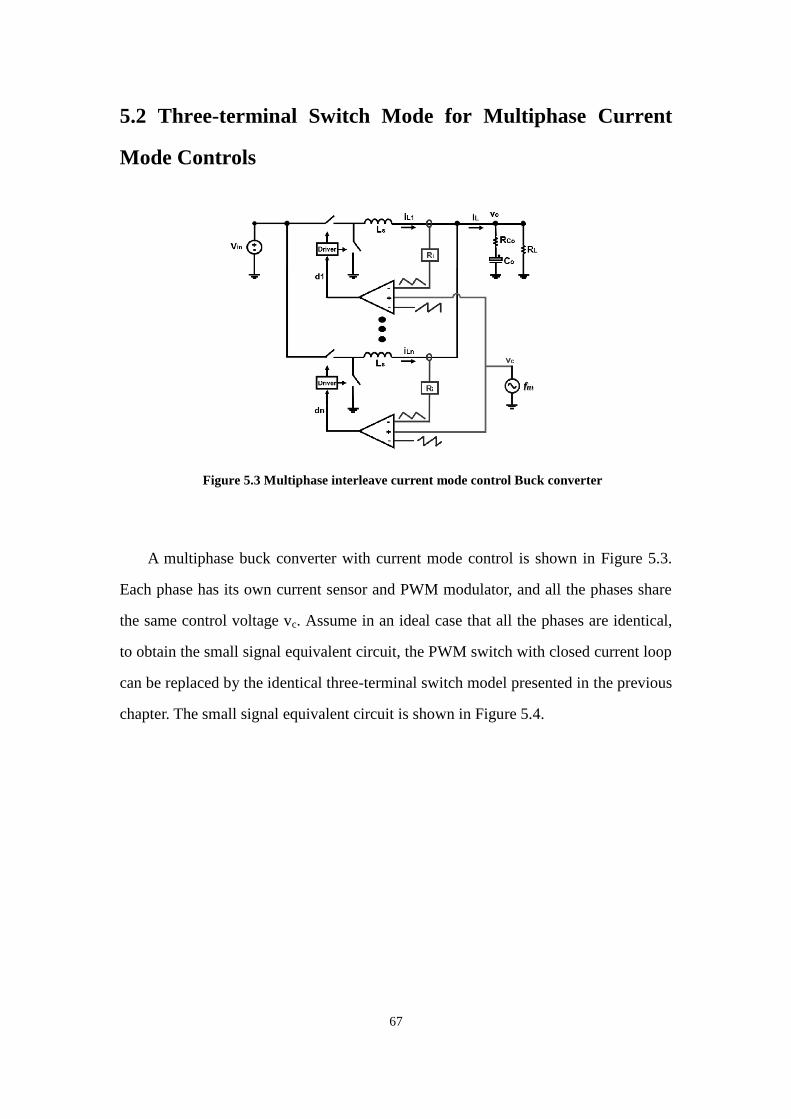
67
5.2 Three-terminal Switch Mode for Multiphase Current
Mode Controls
Figure 5.3 Multiphase interleave current mode control Buck converter
A multiphase buck converter with current mode control is shown in Figure 5.3.
Each phase has its own current sensor and PWM modulator, and all the phases share
the same control voltage vc. Assume in an ideal case that all the phases are identical,
to obtain the small signal equivalent circuit, the PWM switch with closed current loop
can be replaced by the identical three-terminal switch model presented in the previous
chapter. The small signal equivalent circuit is shown in Figure 5.4.
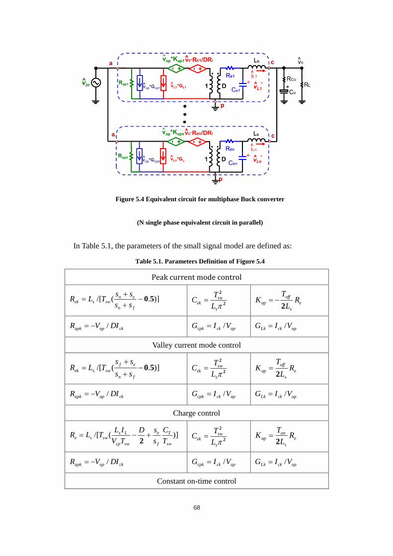
68
Figure 5.4 Equivalent circuit for multiphase Buck converter
(N single phase equivalent circuit in parallel)
In Table 5.1, the parameters of the small signal model are defined as:
Table 5.1. Parameters Definition of Figure 5.4
Peak current mode control
)].(/[ 50
fn
enswsek
ss
ssTLR
2
2
s
swek
L
TC e
s
off
ap RL
TK
2
ckapapk DIVR / apckcpk VIG /
apckLk VIG /
Valley current mode control
)].(/[ 50
fn
ef
swsekss
ssTLR
2
2
s
swek
L
TC e
s
off
ap RL
TK
2
ckapapk DIVR / apckcpk VIG /
apckLk VIG /
Charge control
)](/[sw
T
f
e
swcp
Lsswse
T
C
s
sD
TV
ILTLR
2
2
2
s
swek
L
TC e
s
onap R
L
TK
2
ckapapk DIVR / apckcpk VIG /
apckLk VIG /
Constant on-time control
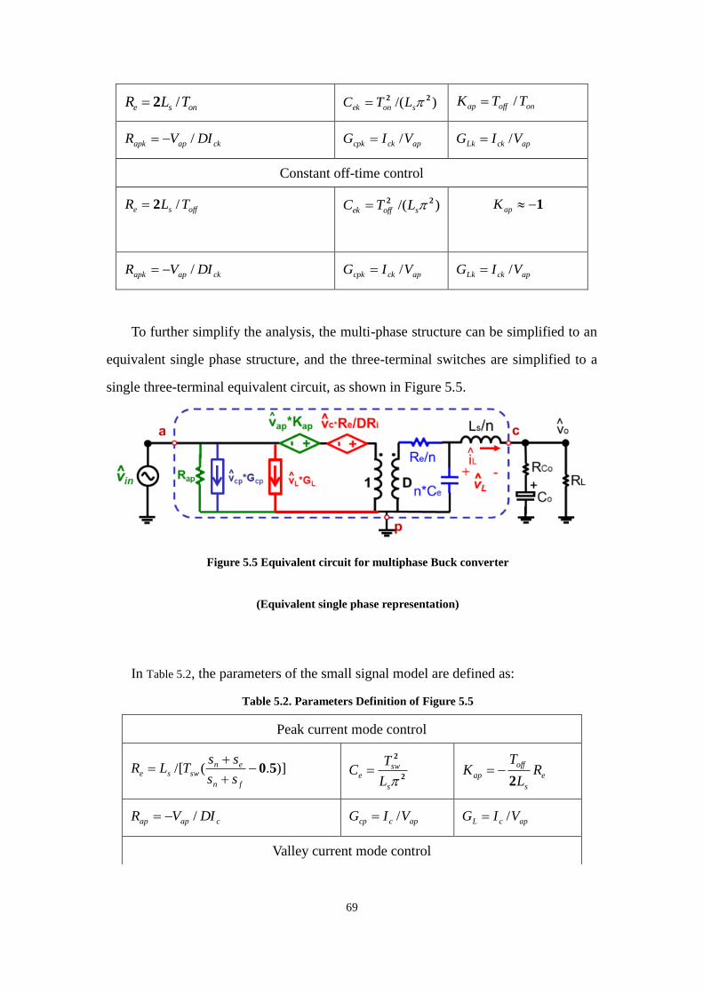
69
onse TLR /2 )/( 22 sonek LTC onoffap TTK /
ckapapk DIVR / apckcpk VIG /
apckLk VIG /
Constant off-time control
offse TLR /2 )/( 22 soffek LTC
1apK
ckapapk DIVR / apckcpk VIG /
apckLk VIG /
To further simplify the analysis, the multi-phase structure can be simplified to an
equivalent single phase structure, and the three-terminal switches are simplified to a
single three-terminal equivalent circuit, as shown in Figure 5.5.
Figure 5.5 Equivalent circuit for multiphase Buck converter
(Equivalent single phase representation)
In Table 5.2, the parameters of the small signal model are defined as:
Table 5.2. Parameters Definition of Figure 5.5
Peak current mode control
)].(/[ 50
fn
enswse
ss
ssTLR
2
2
s
swe
L
TC e
s
off
ap RL
TK
2
capap DIVR / apccp VIG /
apcL VIG /
Valley current mode control
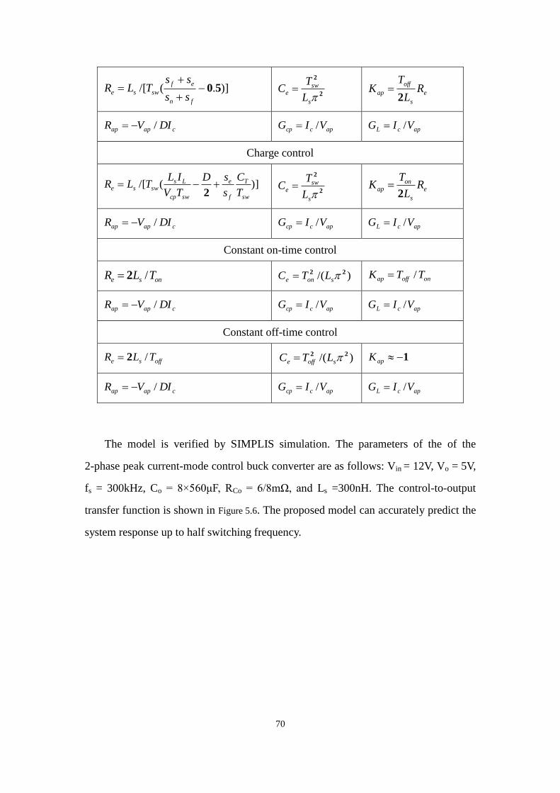
70
)].(/[ 50
fn
ef
swsess
ssTLR
2
2
s
swe
L
TC e
s
off
ap RL
TK
2
capap DIVR / apccp VIG /
apcL VIG /
Charge control
)](/[sw
T
f
e
swcp
Lsswse
T
C
s
sD
TV
ILTLR
2
2
2
s
swe
L
TC e
s
onap R
L
TK
2
capap DIVR / apccp VIG /
apcL VIG /
Constant on-time control
onse TLR /2 )/( 22 sone LTC onoffap TTK /
capap DIVR / apccp VIG /
apcL VIG /
Constant off-time control
offse TLR /2 )/( 22 soffe LTC 1apK
capap DIVR / apccp VIG /
apcL VIG /
The model is verified by SIMPLIS simulation. The parameters of the of the
2-phase peak current-mode control buck converter are as follows: Vin = 12V, Vo = 5V,
fs = 300kHz, Co = 8×560μF, RCo = 6/8mΩ, and Ls =300nH. The control-to-output
transfer function is shown in Figure 5.6. The proposed model can accurately predict the
system response up to half switching frequency.
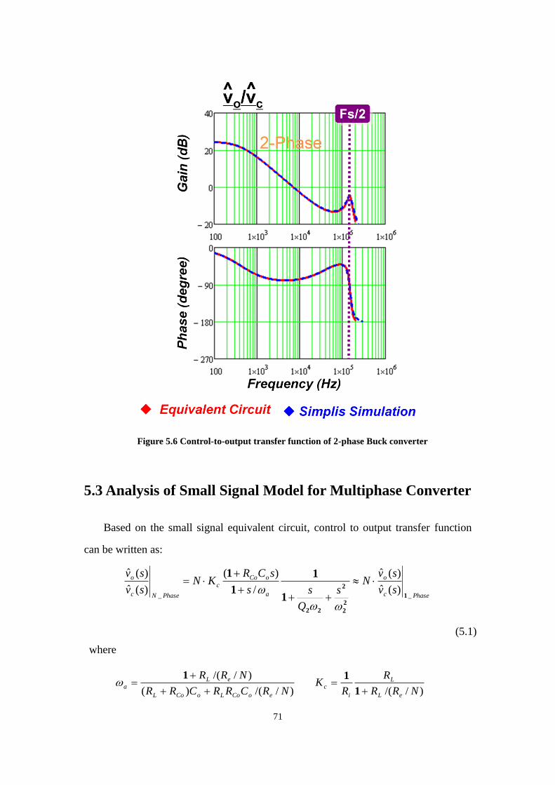
71
Figure 5.6 Control-to-output transfer function of 2-phase Buck converter
5.3 Analysis of Small Signal Model for Multiphase Converter
Based on the small signal equivalent circuit, control to output transfer function
can be written as:
Phasec
o
a
oCo
c
PhaseNc
o
sv
svN
s
Q
ss
sCRKN
sv
sv
__)(ˆ
)(ˆ
/
)(
)(ˆ
)(ˆ
12
2
2
22
1
1
1
1
where
)//()(
)//(
NRCRRCRR
NRR
eoCoLoCoL
eLa
1
)//( NRR
R
RK
eL
L
i
c
1
1
(5.1)
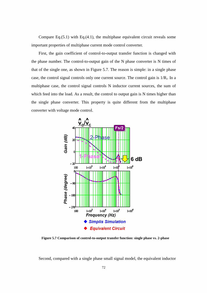
72
Compare Eq.(5.1) with Eq.(4.1), the multiphase equivalent circuit reveals some
important properties of multiphase current mode control converter.
First, the gain coefficient of control-to-output transfer function is changed with
the phase number. The control-to-output gain of the N phase converter is N times of
that of the single one, as shown in Figure 5.7. The reason is simple: in a single phase
case, the control signal controls only one current source. The control gain is 1/Ri. In a
multiphase case, the control signal controls N inductor current sources, the sum of
which feed into the load. As a result, the control to output gain is N times higher than
the single phase converter. This property is quite different from the multiphase
converter with voltage mode control.
Figure 5.7 Comparison of control-to-output transfer function: single phase vs. 2-phase
Second, compared with a single phase small signal model, the equivalent inductor
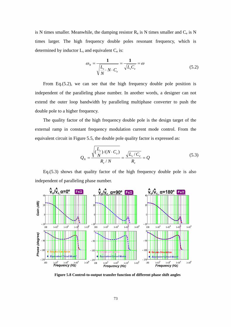
73
is N times smaller. Meanwhile, the damping resistor Re is N times smaller and Ce is N
times larger. The high frequency double poles resonant frequency, which is
determined by inductor Ls and equivalent Ce is:
es
es
NCL
CNN
L
11
(5.2)
From Eq.(5.2), we can see that the high frequency double pole position is
independent of the paralleling phase number. In another words, a designer can not
extend the outer loop bandwidth by paralleling multiphase converter to push the
double pole to a higher frequency.
The quality factor of the high frequency double pole is the design target of the
external ramp in constant frequency modulation current mode control. From the
equivalent circuit in Figure 5.5, the double pole quality factor is expressed as:
QR
CL
NR
CNN
L
Qe
es
e
es
N
/
/
)/()(
(5.3)
Eq.(5.3) shows that quality factor of the high frequency double pole is also
independent of paralleling phase number.
Figure 5.8 Control-to-output transfer function of different phase shift angles
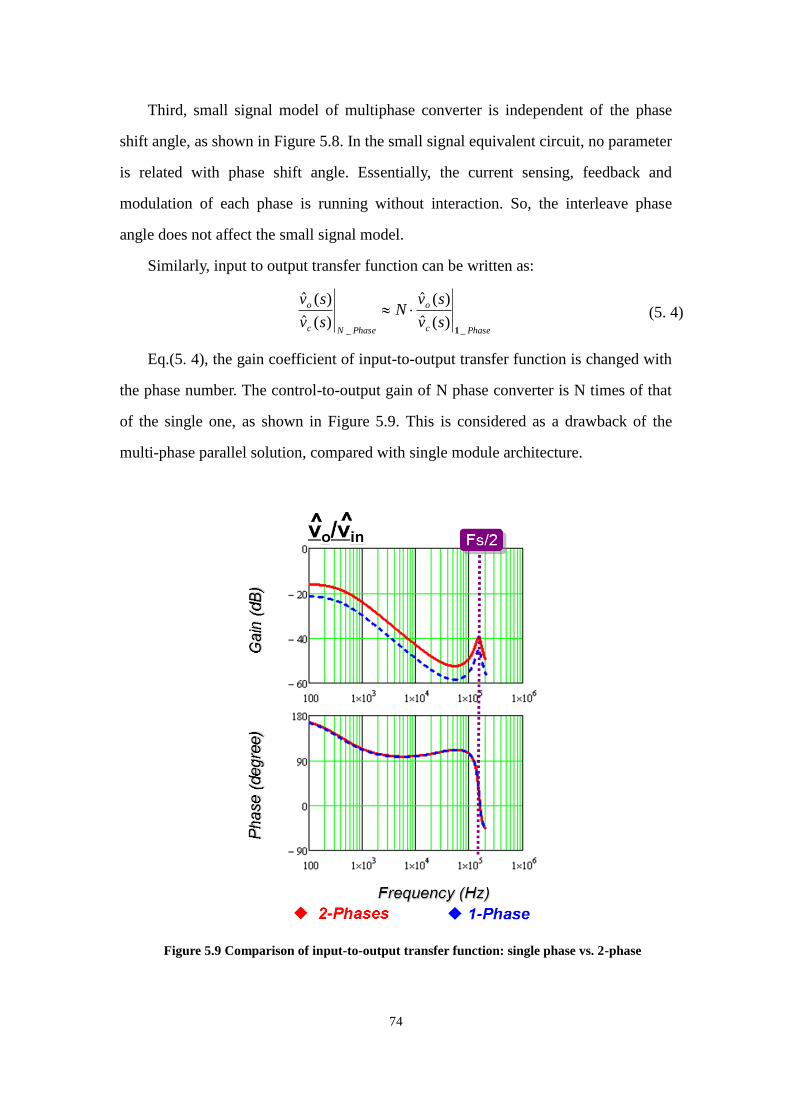
74
Third, small signal model of multiphase converter is independent of the phase
shift angle, as shown in Figure 5.8. In the small signal equivalent circuit, no parameter
is related with phase shift angle. Essentially, the current sensing, feedback and
modulation of each phase is running without interaction. So, the interleave phase
angle does not affect the small signal model.
Similarly, input to output transfer function can be written as:
Phasec
o
PhaseNc
o
sv
svN
sv
sv
__)(ˆ
)(ˆ
)(ˆ
)(ˆ
1
(5. 4)
Eq.(5. 4), the gain coefficient of input-to-output transfer function is changed with
the phase number. The control-to-output gain of N phase converter is N times of that
of the single one, as shown in Figure 5.9. This is considered as a drawback of the
multi-phase parallel solution, compared with single module architecture.
Figure 5.9 Comparison of input-to-output transfer function: single phase vs. 2-phase
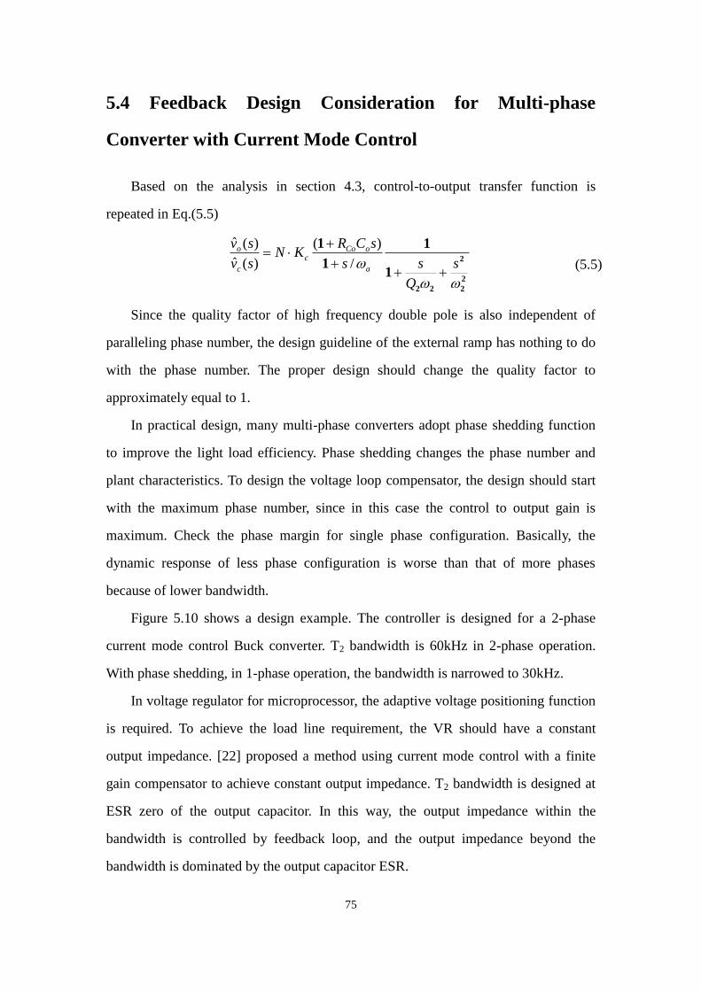
75
5.4 Feedback Design Consideration for Multi-phase
Converter with Current Mode Control
Based on the analysis in section 4.3, control-to-output transfer function is
repeated in Eq.(5.5)
2
2
2
22
1
1
1
1
s
Q
ss
sCRKN
sv
sv
a
oCoc
c
o
/
)(
)(ˆ
)(ˆ
(5.5)
Since the quality factor of high frequency double pole is also independent of
paralleling phase number, the design guideline of the external ramp has nothing to do
with the phase number. The proper design should change the quality factor to
approximately equal to 1.
In practical design, many multi-phase converters adopt phase shedding function
to improve the light load efficiency. Phase shedding changes the phase number and
plant characteristics. To design the voltage loop compensator, the design should start
with the maximum phase number, since in this case the control to output gain is
maximum. Check the phase margin for single phase configuration. Basically, the
dynamic response of less phase configuration is worse than that of more phases
because of lower bandwidth.
Figure 5.10 shows a design example. The controller is designed for a 2-phase
current mode control Buck converter. T2 bandwidth is 60kHz in 2-phase operation.
With phase shedding, in 1-phase operation, the bandwidth is narrowed to 30kHz.
In voltage regulator for microprocessor, the adaptive voltage positioning function
is required. To achieve the load line requirement, the VR should have a constant
output impedance. [22] proposed a method using current mode control with a finite
gain compensator to achieve constant output impedance. T2 bandwidth is designed at
ESR zero of the output capacitor. In this way, the output impedance within the
bandwidth is controlled by feedback loop, and the output impedance beyond the
bandwidth is dominated by the output capacitor ESR.
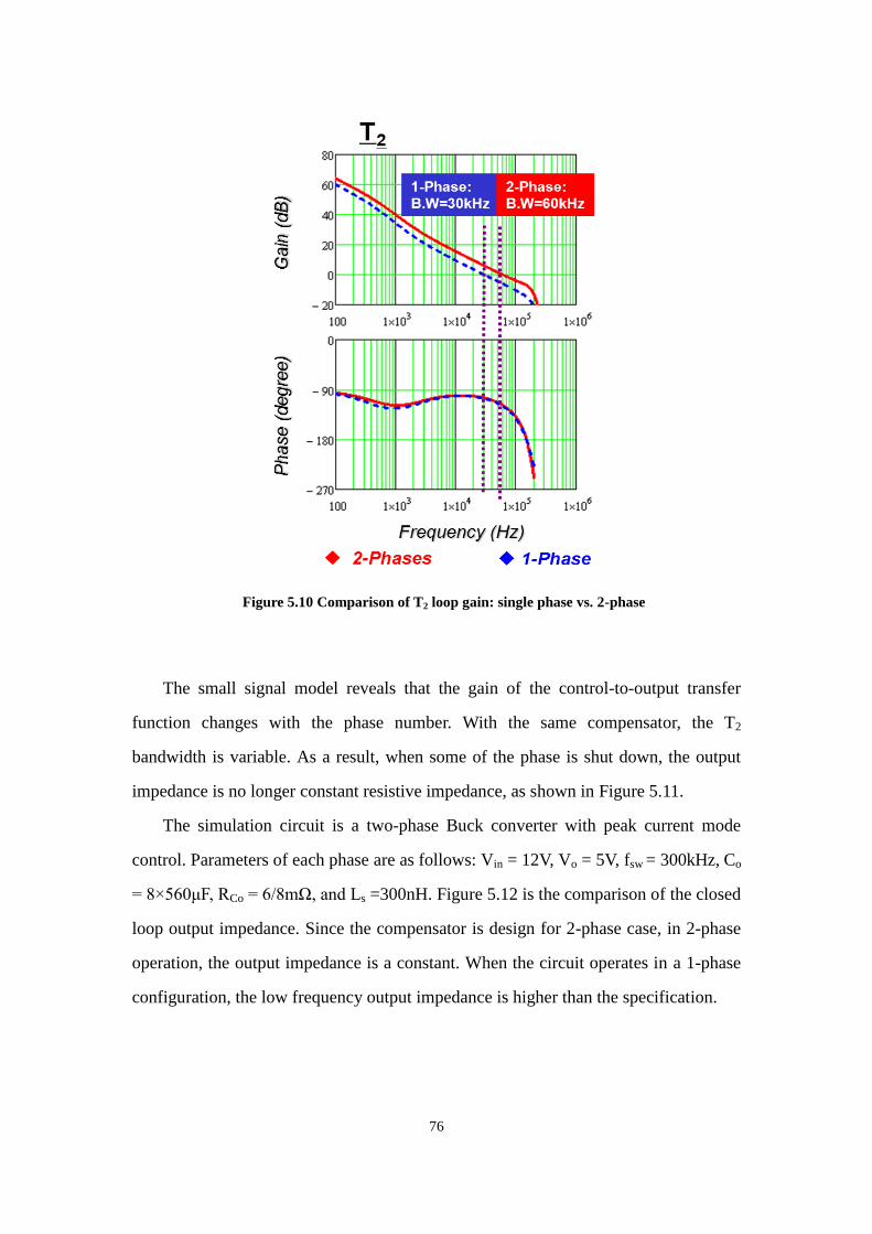
76
Figure 5.10 Comparison of T2 loop gain: single phase vs. 2-phase
The small signal model reveals that the gain of the control-to-output transfer
function changes with the phase number. With the same compensator, the T2
bandwidth is variable. As a result, when some of the phase is shut down, the output
impedance is no longer constant resistive impedance, as shown in Figure 5.11.
The simulation circuit is a two-phase Buck converter with peak current mode
control. Parameters of each phase are as follows: Vin = 12V, Vo = 5V, fsw = 300kHz, Co
= 8×560μF, RCo = 6/8mΩ, and Ls =300nH. Figure 5.12 is the comparison of the closed
loop output impedance. Since the compensator is design for 2-phase case, in 2-phase
operation, the output impedance is a constant. When the circuit operates in a 1-phase
configuration, the low frequency output impedance is higher than the specification.
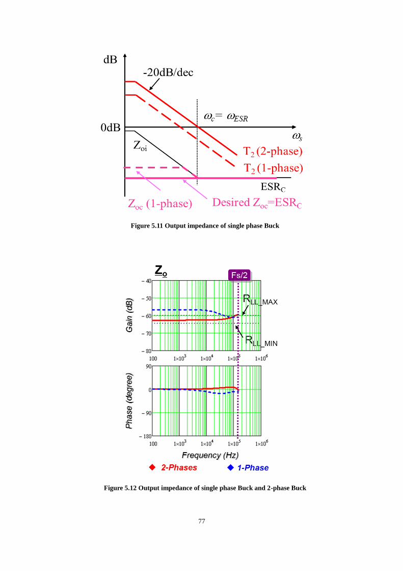
77
Figure 5.11 Output impedance of single phase Buck
Figure 5.12 Output impedance of single phase Buck and 2-phase Buck

78
To solve this problem, compensator can use adaptive gain according to the phase
number. The other way is to change the current sensing gain to be inversely
proportional to the phase number. The implementation of adaptive control is out of the
discussion area of this thesis.
5.5 Summary
The three-terminal switch model is extended to a multiphase current mode control.
Some design concerns are discussed based on the model.
79
Chapter 6. Conclusion
6.1 Summary
Current-mode control architectures with different implementation approaches
have been an indispensable technique in many applications, such as voltage regulator,
power factor correction, battery charger and LED driver. Since the inductor current
ramp, one of the state variables influenced by the input voltage and the output voltage,
is used in the modulator in current-mode control without any low pass filter, high
order harmonics play important role in the feedback control. This is why it is difficult
to obtain the small-signal model for current-mode control in the frequency domain.
Continuous time domain model proposed recently successfully model the
current-mode control architectures with different implementation. However, the
model was derived from describing function method, which is very mathematically
complicated and also time consuming. Although an equivalent circuit for current
mode control Buck converter was proposed to help designers to use the model without
involving complicated math, the equivalent circuit is not a complete model. Moreover,
no equivalent circuit for other topologies is available for designers. In this thesis, the
primary objective is to develop a unified three-terminal switch model for
current-mode control with different implementation methods, which are applicable in
all the current mode control power converters.
First, the existing model for the current mode control is reviewed. The
limitation of average models and discrete time model for the current-mode control is
identified. The continuous time model and its equivalent circuit of Buck converter is
introduced. The deficiency of the equivalent circuit is discussed.
After that, a unified three-terminal switch model for current mode control is
presented. Based on the observation, the PWM switch and the closed current loop is
taken as an invariant sub-circuit, which is common to different DC/DC converter
topologies. A basic small signal relationship is studied and the result shows that the
80
PWM switch with current feedback preserves the property of the PWM switch. A
three-terminal equivalent circuit is developed to represent the small signal behavior of
this common sub-circuit. The proposed model is a unified model which is applicable
in both constant frequency modulation and variable frequency modulation. The
physical meaning of the three-terminal equivalent circuit model is discussed. The
model is verified by SIMPLIS simulation in commonly used converters for both
constant frequency modulation and variable frequency modulation.
Then, based on the proposed unified model, a comparison between different
current mode control implementations is presented. In different applications, different
implementations have their unique benefit on extending control bandwidth. The
properties of audio susceptibility and output impedance are discussed. It is found that,
for adaptive voltage positioning design, constant on-time current mode control can
simplifiy the outer loop design.
Next, since multiphase interleaving structure is widely used in PFC, voltage
regulator and other high current applications, the model is extended to multiphase
current mode control. Some design concerns are discussed based on the model.
As a conclusion, a unified three-terminal switch model for current mode
controls is investigated. The proposed model is quite general and not limited by
implementation methods and topologies. All the modeling results are verified
through simulation and experiments.
6.2 Future Works
In the thesis, a three-terminal switch model is proposed to characterize the small
signal model of current mode control converters, including peak current mode control,
valley current mode control, charge control and constant on-time control and constant
off-time control. The equivalent circuit model might be extended to average current
mode control and hysteresis current mode control. Furthermore, it could be interesting

81
to develop an equivalent circuit model for V2 control, which suffers from high
frequency sub-harmonic oscillation problem.
82
Reference
[1] L. E. Galllaher, “Current Regulator with AC and DC Feedback,” U.S. Patent
3,350,628, 1967.
[2] F. C. Schwarz, “Analog Signal to Discrete Time Interval Converter (ASDTIC),”
U. S. Patent 3,659,184, 1972.
[3] A. Capel, G. Ferrante, D. O’Sullivan, and A. Weinberg, “Application of the
Injected Current Model for the Dynamic Analysis of Switching Regulators with
the New Concept of LC3 Modulator,” in proc. IEEE PESC’78, pp. 135-147.
[4] A. D. Schoenfeld, Y. Yu, “ASDTIC Control and Standardized Interface Circuits
Applied to Buck, Parallel and Buck-Boost DC-to-DC Power Converters,” NASA
Report NASA CR-121106, February, 1973.
[5] C. W. Deisch, “Switching Control Method Changes Power Converter into a
Current Source,” in proc. IEEE PESC’78, pp. 300-306.
[6] R. Redl and N. O. Sokal, “Current-mode control, five different types, used with
the three basic classes of power converters: small-signal ac and large-signal dc
characterization, stability requirements, and implementation of practical circuits,”
in Proc. IEEE PESC’85, pp. 771-785.
[7] W.Tang, Y.Jiang, G.C.Hua, F.C.Lee, I.Cohen, “Power Factor Correction With
Flyback Converter Employing Charge Control” in Proc. IEEE APEC’93, pp. 293
– 298, 1993.
[8] P. L. Hunter, “Converter Circuit and Method Having Fast Responding Current
Balance and Limiting,” U.S. Patent 4,002,963, 1977.
[9] L.H. Dixon, “Average Current-Mode Control of Switching Power Supplies,”
Unitrode Power Supply Design Seminar handbook, 1990, pp. 5.1-5.14
[10] I. Cohen, “Adaptive control method for power converters,” U. S. Patent
5,438,505, 1995.
83
[11] J. P. Bryant, “AC-DC power supply growth variation in China and North
America,” in proc. IEEE APEC’05, pp.159-162.
[12] S. Varma, “Future power solutions,” Special Session Presentation of IEEE APEC,
2005.
[13] E. Stanford, “Power delivery challenges in computer platforms,” Special Session
Presentation of IEEE APEC, 2006.
[14] B. Mammano, “Distributed power system,” Unitrode Seminar, SEM-900, 1993.
[15] F. C. Lee, P. Barbosa, P. Xu, J. Zhang, B. Yang, and F. Canales, “Topologies and
design considerations for distributed power system applications,” in proc. IEEE,
vol. 89, no. 6, Jun. 2001, pp. 939–950.
[16] P. Xu, W. Chen, J. Shao, P.-L. Wong, B. Yang, and F. C. Lee, “Development of 1
kW front-end module for DPS testbed,” in proc.CPES Annual Seminar, 2000, pp.
116-119.
[17] B. Yang, “Topology Investigation for Front End DC/DC Power Conversion for
Distributed Power System”, Ph. D Dissertation, Virginia Tech, Blacksburg,
2003.
[18] B. Lu, “Investigation of High-density Integrated Solution for AC/DC Conversion
of a Distributed Power System”, Ph. D Dissertation, Virginia Tech, Blacksburg,
2006.
[19] J. Sun, “Dynamic Performance Analyses of Current Sharing Control for DC/DC
Converters,” Ph. D. dissertation, Virginia Tech., 2007
[20] Intel document, “Voltage Regulator-Down (VRD) 11.0 Processor Power
Delivery Design Guidelines for Desktop LGA775 Socket,” November, 2006,
Available at http://www.intel.com.
[21] R. Redl, B. P. Erisman and Z. Zansky, “Optimizing the Load Transient Response
of the Buck Converter,”in proc. IEEE APEC’98, pp. 170-176.
84
[22] K. Yao, Y. Meng, P. Xu and F. C. Lee, “Design Considerations for VRM
Transient Response Based on the Output Impedance,” in proc. IEEE APEC’02,
pp. 14-20.
[23] K. Yao, M. Xu, Y. Meng, and F. C. Lee, “Design considerations for VRM
transient response based on theoutput impedance,” IEEE Trans. Power Electron.,
Vol. 19, Issue 6, Nov. 2004, pp. 1454-1461.
[24] K. Yao, K. Lee, M. Xu, and F. C. Lee, “Optimal design of the active droop
control method for the transient response,” in proc. IEEE APEC’03, pp. 718-723.
[25] K. Yao, Y. Ren, J. Sun, K. Lee, M. Xu, J.i Zhou and F. C. Lee, “Adaptive Voltage
Position Design for Voltage Regulators,” in proc. IEEE APEC’04, pp. 272-278.
[26] J.P.Gegner, C.Q.Lee, “Linear peak current mode control a: simple active power
factor correction co ntrol,” in proc. IEEE PESC '96, pp. 196 - 202.
[27] C. Adragna, “AN1792 Design of fixed-off-time- controlled pfc pre-regulators
with the l6562,” ST Semiconductor Application Note, 2003.
[28] C.Adragna, S.De Simone, G.Gattavari, “New Fixed Off-Time PWM Modulator
Provides Constant Frequency Operation in Boost PFC Pre-regulators,” in proc.
SPEEDAM’08, pp. 656 - 661.
[29] Maxim, MAX8713 datasheet,
http://datasheets.maxim-ic.com/en/ds/MAX8713.pdf
[30] Linear Technology, LTC1980 datasheet,
http://cds.linear.com/docs/Datasheet/1980f.pdf
[31] E.F. Schubert, “Light-emitting diodes(Second Edition)”, Cambridge University
Press, 2006.
[32] LUMILEDS, "Luxeon III Emitter Technical Datasheet DS45",
http://www.sparkfun.com/datasheets/Components/Luxeon-III.pdf
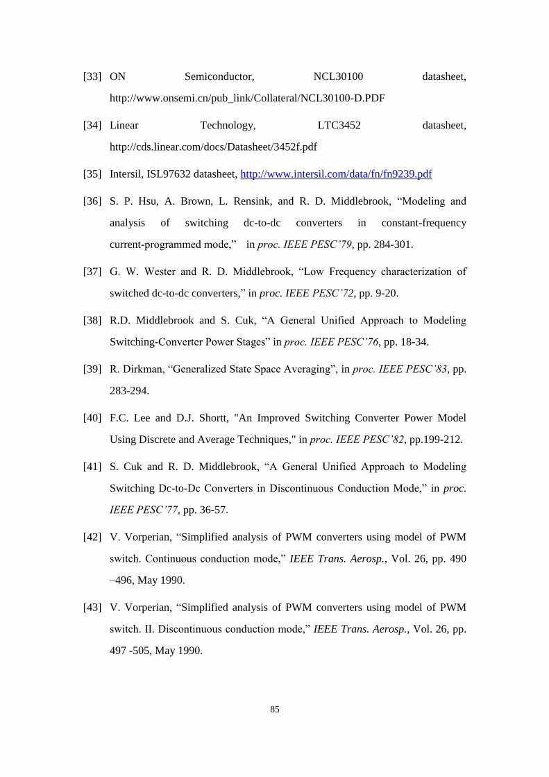
85
[33] ON Semiconductor, NCL30100 datasheet,
http://www.onsemi.cn/pub_link/Collateral/NCL30100-D.PDF
[34] Linear Technology, LTC3452 datasheet,
http://cds.linear.com/docs/Datasheet/3452f.pdf
[35] Intersil, ISL97632 datasheet, http://www.intersil.com/data/fn/fn9239.pdf
[36] S. P. Hsu, A. Brown, L. Rensink, and R. D. Middlebrook, “Modeling and
analysis of switching dc-to-dc converters in constant-frequency
current-programmed mode,” in proc. IEEE PESC’79, pp. 284-301.
[37] G. W. Wester and R. D. Middlebrook, “Low Frequency characterization of
switched dc-to-dc converters,” in proc. IEEE PESC’72, pp. 9-20.
[38] R.D. Middlebrook and S. Cuk, “A General Unified Approach to Modeling
Switching-Converter Power Stages” in proc. IEEE PESC’76, pp. 18-34.
[39] R. Dirkman, “Generalized State Space Averaging”, in proc. IEEE PESC’83, pp.
283-294.
[40] F.C. Lee and D.J. Shortt, "An Improved Switching Converter Power Model
Using Discrete and Average Techniques," in proc. IEEE PESC’82, pp.199-212.
[41] S. Cuk and R. D. Middlebrook, “A General Unified Approach to Modeling
Switching Dc-to-Dc Converters in Discontinuous Conduction Mode,” in proc.
IEEE PESC’77, pp. 36-57.
[42] V. Vorperian, “Simplified analysis of PWM converters using model of PWM
switch. Continuous conduction mode,” IEEE Trans. Aerosp., Vol. 26, pp. 490
–496, May 1990.
[43] V. Vorperian, “Simplified analysis of PWM converters using model of PWM
switch. II. Discontinuous conduction mode,” IEEE Trans. Aerosp., Vol. 26, pp.
497 -505, May 1990.
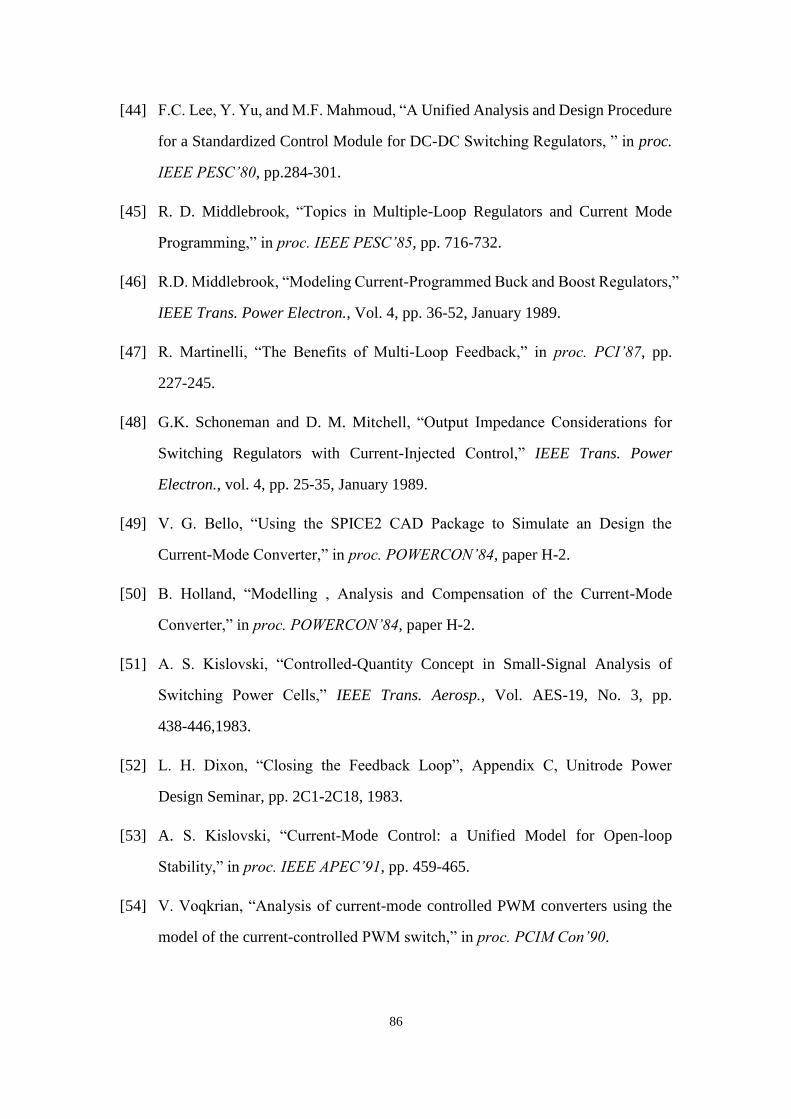
86
[44] F.C. Lee, Y. Yu, and M.F. Mahmoud, “A Unified Analysis and Design Procedure
for a Standardized Control Module for DC-DC Switching Regulators, ” in proc.
IEEE PESC’80, pp.284-301.
[45] R. D. Middlebrook, “Topics in Multiple-Loop Regulators and Current Mode
Programming,” in proc. IEEE PESC’85, pp. 716-732.
[46] R.D. Middlebrook, “Modeling Current-Programmed Buck and Boost Regulators,”
IEEE Trans. Power Electron., Vol. 4, pp. 36-52, January 1989.
[47] R. Martinelli, “The Benefits of Multi-Loop Feedback,” in proc. PCI’87, pp.
227-245.
[48] G.K. Schoneman and D. M. Mitchell, “Output Impedance Considerations for
Switching Regulators with Current-Injected Control,” IEEE Trans. Power
Electron., vol. 4, pp. 25-35, January 1989.
[49] V. G. Bello, “Using the SPICE2 CAD Package to Simulate an Design the
Current-Mode Converter,” in proc. POWERCON’84, paper H-2.
[50] B. Holland, “Modelling , Analysis and Compensation of the Current-Mode
Converter,” in proc. POWERCON’84, paper H-2.
[51] A. S. Kislovski, “Controlled-Quantity Concept in Small-Signal Analysis of
Switching Power Cells,” IEEE Trans. Aerosp., Vol. AES-19, No. 3, pp.
438-446,1983.
[52] L. H. Dixon, “Closing the Feedback Loop”, Appendix C, Unitrode Power
Design Seminar, pp. 2C1-2C18, 1983.
[53] A. S. Kislovski, “Current-Mode Control: a Unified Model for Open-loop
Stability,” in proc. IEEE APEC’91, pp. 459-465.
[54] V. Voqkrian, “Analysis of current-mode controlled PWM converters using the
model of the current-controlled PWM switch,” in proc. PCIM Con’90.
87
[55] D. J. Packard, “Discrete Modeling and Analysis of Switching Regulators,” Ph.D.
dissertation, Cal. Tech., CA, May 1976
[56] A. R. Brown and R. D. Middlebrook, “Sample-Data Modeling of Switched
Regulators,” in proc. IEEE PESC’81, pp. 349-369.
[57] G. C. Verghese, C. A. Bruzos, and K. N. Mahabir, “Averaged and sample-data
models for current mode control: A reexamination,” in Proc. IEEE PESC’89, pp.
484-491.
[58] R. Redl, “High-frequency extension of the small-signal model of the
constant-frequency current-mode-controlled converter,” in proc. IEEE APEC '91,
pp. 466 – 472.
[59] R. B. Ridley, “A new, continuous-time model for current-mode control,” IEEE
Trans. Power Electron., vol. 6, no. 2, pp. 271-280, April 1991.
[60] R. Tymerski and D. Li, “State-space models for current-programmed
pulsewidth-modulated converters,” IEEE Trans. Power Electron., vol.8, no. 3, pp.
271-278, July 1993.
[61] F. D. Tan and R. D. Middlebrook, “A unfied model for current-programmed
converters,” IEEE Trans. Power Electron., vol. 10, no. 4, pp.397–408, Jul. 1995.
[62] D. J. Perreault and G. C. Verghese, “Time-varying effects for current-mode
control,” in proc. IEEE PESC’95, pp. 621-628.
[63] M. K. Kazimierczuk, “Transfer function of current modulator in pwm
converters with current-mode control,” IEEE Trans. Circuits and Systems I, vol.
47, no. 9, pp. 1407-1412, Sep. 2000.
[64] E. A. Mayer and A. J. King, “An improved sampled-data current-mode control
which explains the effects of the control delay,” IEEE Trans. Power Electron.,
vol. 16, no. 3, pp. 369-374, May. 2001.
88
[65] B. Bryant and M. K. Kazimierczuk, “Modeling the closed-current loop of pwm
dc-dc converters operating in ccm with peak current-mode control,” IEEE Trans.
Circuits and Systems, vol. 52, no. 11, pp. 2404-2412, Nov. 2005.
[66] W. Tang, F. C. Lee, and R. B. Ridley, “Small-signal modeling of average
current-mode control,” IEEE Trans. Power Electron., vol. 8, pp. 112-119, April
1993.
[67] W. Tang, F. C. Lee, R. B. Ridley, and I. Cohen, “Charge control: modeling,
analysis, and design,” IEEE Trans. Power Electron., vol. 8, pp. 396-403, Oct.
1993.
[68] Y.-W. Lo and R. J. King, “Sampled-data modeling of the average-input
current-mode-controlled buck converter”, IEEE Trans. Power Electron., vol. 14,
no. 5, pp. 918-927, Sept. 1999.
[69] R. B. Ridley, “A new continuous-time model for current-mode control with
constant frequency, constant on-time, and constant off-time, in CCM and DCM,”
in proc. IEEE PESC’90, pp. 382- 389.
[70] J. Li, “Current-Mode Control: Modeling and its Digital Application,” Ph. D.
Dissertation, Virginia Tech, 2009.
[71] A. Gelb, and W. E. Vander Velde: Multiple-Input Describing Functions and
Nonlinear System Design, McGraw Hill, 1968.
[72] Xiaoru Xu, Xiaobo Wu, Xiaolang Yan, “A Quasi Fixed Frequency Constant On
Time Controlled Boost Converter,” in proc. IEEE ISCAS’08, pp. 2206 – 2209,
2008.
[73] Xiaoming Duan, A.Q.Huang, “Current-Mode Variable-Frequency Control
Architecture for High-Current Low-Voltage DC–DC Converters,” IEEE Trans.
Power Electron., vol. 21, pp. 1133 - 1137, July 2006.
89
[74] J.T.Mossoba, P.T.Krein, “Output Impedance of High Performance Current
Mode dc-dc Buck Converters, with Applications to Voltage-Regulator Module
Control Combinations,” in proc. IEEE APEC '04, pp. 1315 - 1321.
[75] N.Kondrath, M.K.Kazimierczuk, “Control-to-Output and Duty
Ratio-to-Inductor Current Transfer Functions of Peak Current-Mode Controlled
DC-DC PWM Buck Converter in CCM,” in proc. IEEE ISCAS '10, pp. 2734 -
2737.
[76] C. Wang, “Investigation on Interleaved Boost Converters and Applications,” Ph.
D. Dissertation, Virginia Tech, 2009.
[77] R. Redl, “Small-signal high-frequency analysis of the free-running
current-mode-controlled converter,” in proc. IEEE PESC '91, pp. 897 – 906.
[78] R. D. Middlebrook, “Predicting modulator phase lag in PWM converter feedback
loops,” In proc. POWERCON’ 81, paper H-4.


![Lecture 6 - Terminal Operation III (Touched Up) [Compatibility Mode]](https://img.pdfslide.us/doc/110x75/577d1fae1a28ab4e1e91157d/lecture-6-terminal-operation-iii-touched-up-compatibility-mode.jpg)