Embed Size (px)
Citation preview

Uneven Bin Width Digitization and a Timing Calibration Method Using Cascaded PLL
Wu, Jinyuan
Fermilab
May. 2014

May. 2014, Wu Jinyuan, Fermilab [email protected] Uneven Bin Width Digitization & Cascade PLL 2
Introduction Digitization with uneven bins is needed in FPGA
based TDC. The differential nonlinearity is acceptable in many
cases. A value called equivalent bin width is defined. A scheme of generating calibration pulses with
cascaded PLL circuits is presented. The same scheme can be used for clock phase
measurement.

May. 2014, Wu Jinyuan, Fermilab [email protected] Uneven Bin Width Digitization & Cascade PLL 3
TDC Using FPGA Logic Chain Delay
Convenient. Low cost. But the bin widths are not uniform.
IN
CLK
0
20
40
60
80
100
120
140
160
180
0 16 32 48 64
bin
wid
th (
ps)

Uneven Bin Width Digitization & Cascade PLL 4May. 2014, Wu Jinyuan, Fermilab [email protected]
16 Patterns@ 400 MHz
VCCINT=1.20V
VCCINT=1.18V
Delay Line Speed vs. Core Voltage

5
Adjusting Bin Widths?
Feb. 2014, Wu Jinyuan, Fermilab [email protected] PPS TDC
Compensation: Adjusting bin width to certain value.
Slowing down the delay Chain?
Linearization: Fine tuning width of each bin.
Cost?
DF

6
Nonlinearity = Something Bad?
Feb. 2014, Wu Jinyuan, Fermilab [email protected] PPS TDC
Nonlinear scales are commonly used.
Sometimes, the markers can be in arbitrary (but known) positions, such as in solar spectrum.
solar-spectrum-from-www-mao-kiev-ua--sol_ukr--terskol--bmv_m
Association of Universities for Research in Astronomy Inc. (AURA)

7
The Equivalent Width
Feb. 2014, Wu Jinyuan, Fermilab [email protected] PPS TDC
n-1
W
20 1 3 4 5 6 n n+1
w0 w1 w2 w3 w4
Digitizers with non-uniform bin widths are able to make precise measurements as long as it is calibrated appropriately.
A equivalent bin width can be defined as above. The calibration can be done offline or/and online.
1212
22
eqeqi
i
ieq w
W
ww
weq

May. 2014, Wu Jinyuan, Fermilab [email protected] Uneven Bin Width Digitization & Cascade PLL 8
Auto Calibration: Histogram Booking In the auto calibration process, a bin
width histogram (DNL histogram) is first booked.
More counts are accumulated in wider bins.
0
20
40
60
80
100
120
140
160
180
0 16 32 48 64
bin
wid
th (
ps)
DNLHistogram
In (bin)LUT
S
Out (ps)
16-32KEvents
May. 2014, Wu Jinyuan, Fermilab [email protected] Uneven Bin Width Digitization & Cascade PLL 9
0
500
1000
1500
2000
2500
0 16 32 48 64
bin
tim
e (
ps)
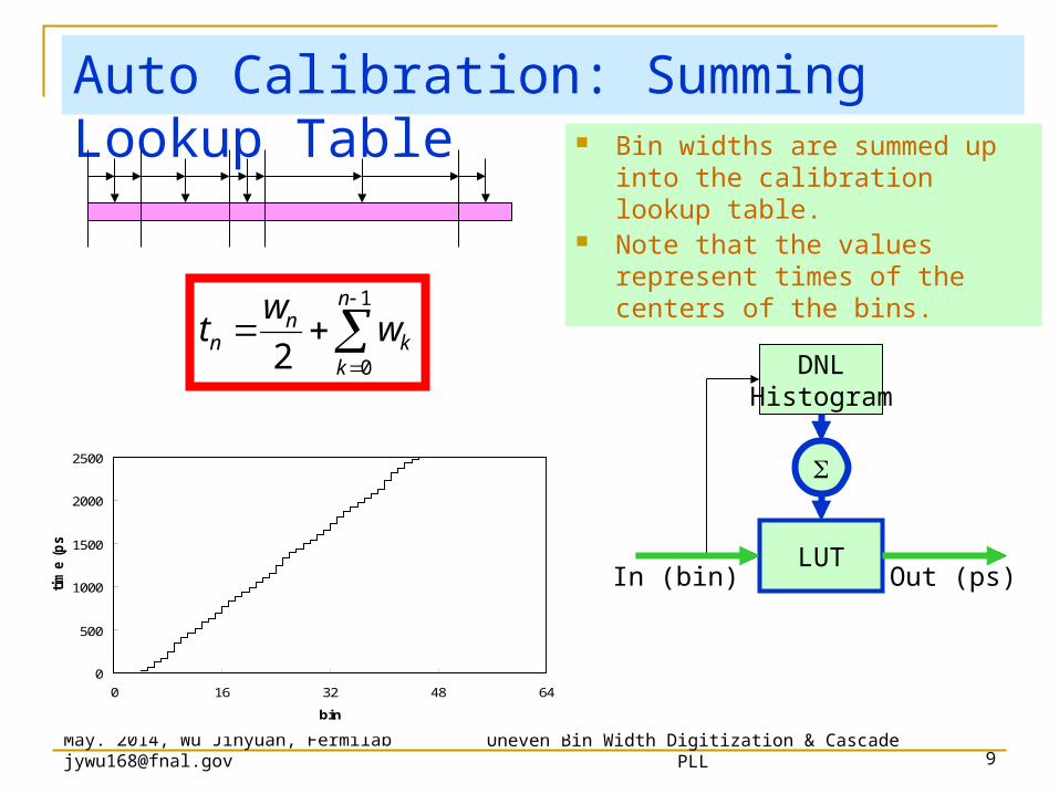
Auto Calibration: Summing Lookup Table Bin widths are summed up into the
calibration lookup table. Note that the values represent times of
the centers of the bins.
DNLHistogram
In (bin)LUT
S
Out (ps)
1
02
n
kk
nn w
wt

May. 2014, Wu Jinyuan, Fermilab [email protected] Uneven Bin Width Digitization & Cascade PLL 10
Calibration Pulse Generation: Random != Uniform
16384 Events
When number of events is finite, random hits has large fluctuations. Pulses with evenly spread timing relative to the TDC clock are desirable.

11
Cascaded PLL Circuits
Feb. 2014, Wu Jinyuan, Fermilab [email protected] PPS TDC
VCCCLOCK_50 INPUT
Cy clone III
inclk0 f requency : 152.381 MHz
Operation Mode: No Compensation
Clk Ratio Ph (dg) DC (%)
c0 105/64 0.00 50.00
inclk0 c0
altpll3
inst25
Cy clone III
inclk0 f requency : 152.381 MHz
Operation Mode: No Compensation
Clk Ratio Ph (dg) DC (%)
c0 64/39 0.00 50.00
inclk0 c0
altpll4
inst30
Cy clone III
inclk0 f requency : 50.000 MHz
Operation Mode: No Compensation
Clk Ratio Ph (dg) DC (%)
c0 64/21 0.00 50.00
inclk0 c0
altpll0
inst21
CK_B
CK250aCK_B
CK251cCK_B
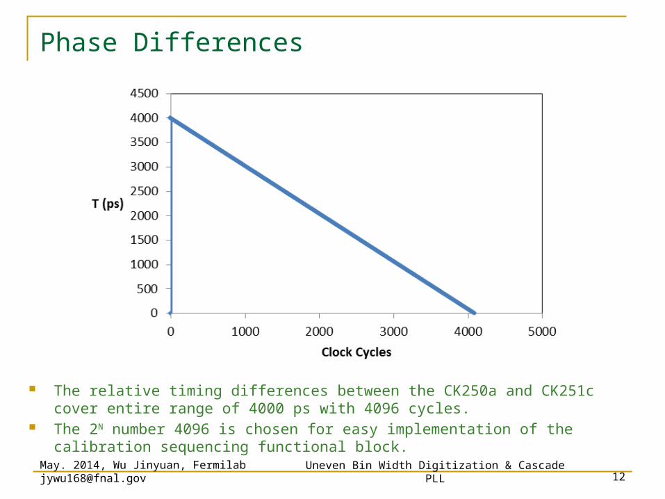
Two stages of PLL circuits are cascaded together. f(CK250a) = 250 MHz f(CK251c) = 250.06 MHz
f(CK251c) = (4096/4095)*f(CK250a)
T(CK250a) - T(CK251c) = 0.97 ps.
CK250a
CK251cCLOCK_50
May. 2014, Wu Jinyuan, Fermilab [email protected] Uneven Bin Width Digitization & Cascade PLL 12
Phase Differences
The relative timing differences between the CK250a and CK251c cover entire range of 4000 ps with 4096 cycles.
The 2N number 4096 is chosen for easy implementation of the calibration sequencing functional block.

May. 2014, Wu Jinyuan, Fermilab [email protected] Uneven Bin Width Digitization & Cascade PLL 13
Test Result in an Oscilloscope Screen Capture
A total of 16384 Calibration edges are collected. Entire 4000 ps range are scanned 4 times (4*4096 = 16384). The histogram (with 50 ps/bin) serves as a demonstration of calibration lookup table.
Trigger EdgesBy CK250a
Calibration EdgesBy CK251c
CalibrationLookup Table

May. 2014, Wu Jinyuan, Fermilab [email protected] Uneven Bin Width Digitization & Cascade PLL 14
Clock Phase Measurement, Another Application
Two clocks from same source but with different phases are multiplied in PLL.
The CK251c clock scans entire 4000 ps range and the correctness of the captures of the DFF driven by two clocks are checked.
D Q D Q
CorrectlyCaptured?
CK250aCK251c
D Q D Q
CorrectlyCaptured?
CK250bCK251c
CascadedPLL
Circuits
CK251c
CK250a
CascadedPLL
Circuits CK250b
CK50a
CK50b

May. 2014, Wu Jinyuan, Fermilab [email protected] Uneven Bin Width Digitization & Cascade PLL 15
Oscilloscope Screen Capture
The phase difference of CK250a and CK250b can be measured after CK251c scans through. The 0-1 and 1-0 transitions have different setup time.
Captured CorrectlyBy CK250a
Captured CorrectlyBy CK250b
Captured 0-1 Trans.By CK250b
Captured 1-0 Trans.By CK250b
4 ns/step => 0.97 ps

The End
Thanks

May. 2014, Wu Jinyuan, Fermilab [email protected] Uneven Bin Width Digitization & Cascade PLL 17
Good, However
Auto calibration solved some problems However, it won’t eliminate the ultra-wide bins
0
20
40
60
80
100
120
140
160
180
0 16 32 48 64
bin
wid
th (
ps)
L
ww i
i
ieq 12
22

Concern: Dead Time?
May. 2014, Wu Jinyuan, Fermilab [email protected] Uneven Bin Width Digitization & Cascade PLL 18

May. 2014, Wu Jinyuan, Fermilab [email protected] Uneven Bin Width Digitization & Cascade PLL 19
Wave Union Launcher A
In
CLK
1: Unleash0: HoldWave UnionLauncher A
Regular TDC records only one transition
Wave Union TDC records multiple transitions.
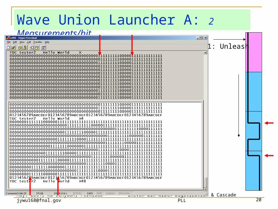
May. 2014, Wu Jinyuan, Fermilab [email protected] Uneven Bin Width Digitization & Cascade PLL 20
Wave Union Launcher A: 2 Measurements/hit
1: Unleash

May. 2014, Wu Jinyuan, Fermilab [email protected] Uneven Bin Width Digitization & Cascade PLL 21
Sub-dividing Ultra-wide Bins
1: Unleash
1
2
1
2
Device: EP2C8T144C6 Plain TDC:
Max. bin width: 160 ps. Equivalent bin width: 60 ps.
Wave Union TDC A: Max. bin width: 65 ps. Equivalent bin width: 30 ps.
0
20
40
60
80
100
120
140
160
180
0 16 32 48 64 80 96 112 128bin
wid
th (p
s)
Plain TDC
Wave Union TDC A

May. 2014, Wu Jinyuan, Fermilab [email protected] Uneven Bin Width Digitization & Cascade PLL 22
Time Measurement Errors Due to Power Supply Noise
Typical RMS resolution is 25-30 ps. Measurements with cleaner power (diamonds) is better than noisy power (squares).
SwitchingPower Supply Linear
Power Supply

May. 2014, Wu Jinyuan, Fermilab [email protected] Uneven Bin Width Digitization & Cascade PLL 23
Pipeline Structure of TDC Time Sensing Block
The front-end of the TDC is designed with pipeline structure.
There is nearly no dead time in this section.
A hit can be digitized every clock cycle (@250 MHz).
However, we introduce some dead time by using slower clock to save power.
Hit Detect Logic
CoarseTimeCounter
FineTimeEncoder
In
CLK
ENA
FineTime
CoarseTime
DataReady

Concern: Low-power?
May. 2014, Wu Jinyuan, Fermilab [email protected] Uneven Bin Width Digitization & Cascade PLL 24
25
DelayLine &
SamplingRegister
Array
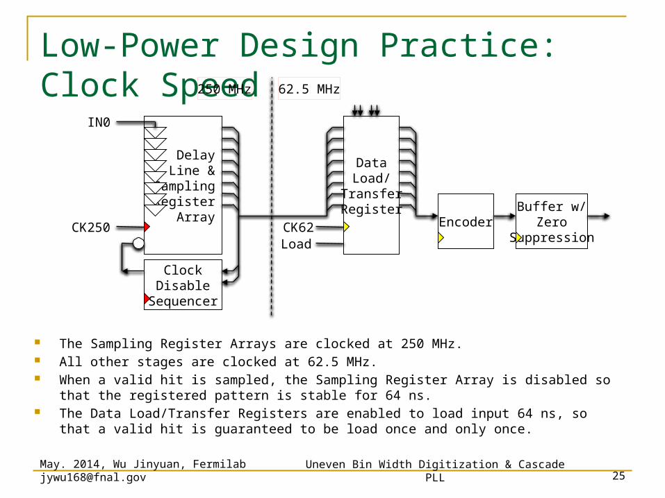
Low-Power Design Practice: Clock Speed
May. 2014, Wu Jinyuan, Fermilab [email protected] Uneven Bin Width Digitization & Cascade PLL
The Sampling Register Arrays are clocked at 250 MHz. All other stages are clocked at 62.5 MHz. When a valid hit is sampled, the Sampling Register Array is disabled so that the registered pattern is stable
for 64 ns. The Data Load/Transfer Registers are enabled to load input 64 ns, so that a valid hit is guaranteed to be load
once and only once.
CK250
DataLoad/
TransferRegister
CK62Load
ClockDisable
Sequencer
Encoder
IN0
Buffer w/Zero
Suppression
250 MHz 62.5 MHz

26
DelayLine &
SamplingRegister
Array
Low Power Design Practice: Resource Sharing
May. 2014, Wu Jinyuan, Fermilab [email protected] Uneven Bin Width Digitization & Cascade PLL
The Data Load/Transfer Registers are enabled to load input 64 ns, (i.e., 4 clock cycles at 62.5 MHz).
The Data Load/Transfer Registers transfer data from other channels when they are not enabled to load.
Four channels share an Encoder and a Buffer with Zero Suppression.
CK250
DataLoad/
TransferRegister
CK62Load
ClockDisable
Sequencer
Encoder
IN0
IN1
IN2
IN3
Buffer w/Zero
Suppression
DataMergingRegister
250 MHz 62.5 MHz

27
Low-Power Design Practice: Wave Union
May. 2014, Wu Jinyuan, Fermilab [email protected] Uneven Bin Width Digitization & Cascade PLL
Intrinsically the Wave Union TDC is a low-power scheme.
Multiple measurements are made with one set of delay line, register encoder etc. yielding finer resolution that otherwise needs several regular TDC blocks to achieve.

Concern: Data Packing?
May. 2014, Wu Jinyuan, Fermilab [email protected] Uneven Bin Width Digitization & Cascade PLL 28

May. 2014, Wu Jinyuan, Fermilab [email protected] Uneven Bin Width Digitization & Cascade PLL 29
Data Packaging: Block Diagram
For each straw, 2 TDC and 1 ADC are implemented. Time and charge data are grouped and sent out together.
1 Straw: 2 TDC + 1 ADC
Carry ChainReg. Array
Encoder
Buffer&
DataPacking
OutputBuffer
Parallel-to-Serial
ConverterData
Carry ChainReg. Array
Encoder
ADCData
1 Straw: 2 TDC + 1 ADC
1 Straw: 2 TDC + 1 ADC

30
Data Packing: A Real Design for a Similar Project
May. 2014, Wu Jinyuan, Fermilab [email protected] Uneven Bin Width Digitization & Cascade PLL
TDC and ADC data packaging for OpenPET of LBL.

31
Data Bit Layout
May. 2014, Wu Jinyuan, Fermilab [email protected] Uneven Bin Width Digitization & Cascade PLL
012345678910111213141516171819202122232425262728293031
CH: 0-15 TDC Fine Time LSB=15.625ps TDC Coarse Time: LSB= 4 ns 0 0 1
Hit
Header & Count Header
ADC 0
0
ADC 1
ADC 2ADC 3
ADC 4ADC 5
ADC 6ADC 7
ADC 8ADC 9
ADC 10ADC 11
TDC Fine Time LSB=15.625ps TDC Coarse Time: LSB= 4 ns 0 0 10
Hit Count
CH: 0-15 TDC Fine Time LSB=15.625ps TDC Coarse Time: LSB= 4 ns 0 0 1
Hit
ADC 0
0
ADC 1
ADC 2ADC 3
ADC 4ADC 5
ADC 6ADC 7
ADC 8ADC 9
ADC 10ADC 11
TDC Fine Time LSB=15.625ps TDC Coarse Time: LSB= 4 ns 0 0 10
Data layout for full ADC resolution. This scheme uses 256 bits/hit. There could be other layout with 128 bits/hit.

32
Connection Between Digitizer and ROC
May. 2014, Wu Jinyuan, Fermilab [email protected] Uneven Bin Width Digitization & Cascade PLL
Clock and frame signals are provided along with data links. Data links runs at 200 M bits/s
Digitizer
ROC
TX
Clock Data
ClockGenerator
RX
Frame
FrameGenerator

33
Data Rate: Is 200 Mb/s Enough?
May. 2014, Wu Jinyuan, Fermilab [email protected] Uneven Bin Width Digitization & Cascade PLL
Assumption: 1695 ns micro-bunch length. 900 ns data taking window. 1 LVDS data output pair for every 4 straws.
The 300 kHz hit rate in TDR is likely an over estimate. As long as the actual hit rate is < 200 kHz, data link of 200 Mb/s per LVDS pair should be
sufficient.
Hit/Straw 256 bits/hit 128 bits/hit
300 kHz 253 Mb/s 126 Mb/s
200 kHz 169 Mb/s 85 Mb/s
100 kHz 85 Mb/s 42 Mb/s
30 kHz 25 Mb/s 12 Mb/s

Test Results
May. 2014, Wu Jinyuan, Fermilab [email protected] Uneven Bin Width Digitization & Cascade PLL 34

May. 2014, Wu Jinyuan, Fermilab [email protected] Uneven Bin Width Digitization & Cascade PLL 35
The Test Hardware
2011
Altera Cyclone III Starter Kit ($211+$50)
FPGA: EP3C25F324C6N ($73.90)
32 channel: 30 ps (25 ps with linear power supply)
27 mW/channel
www.altera.com

May. 2014, Wu Jinyuan, Fermilab [email protected] Uneven Bin Width Digitization & Cascade PLL 36
Test Setup
NIM toLVDSConverter
TDCModule

May. 2014, Wu Jinyuan, Fermilab [email protected] Uneven Bin Width Digitization & Cascade PLL 37
Output Raw Data and Typical Delta T Histogram Between Two Channels
RMS of this histogram is 25 ps.
00003CC064A6F064B8C07CA4F07CB4C094A0F094B0C0AC9CF0ACACC0C497F0C4A8C0DC91F0DCA2

May. 2014, Wu Jinyuan, Fermilab [email protected] Uneven Bin Width Digitization & Cascade PLL 38
Delta T Between NIM Inputs
TDC channels internally ganged together has smallest standard deviation of time differences. Typical channel pairs sharing same fan-out unit has 30 ps RMS. Timing jitters of the fan-out units add to the measurement errors.
0
10
20
30
40
50
60
10 100 1000 10000
sigm
a (p
s)
dt (ps)
8ns 6ns 4ns 2ns
0
500
1000
1500
2000
2500
1500 1700 1900 2100 2300 2500
dt (ps)
HistA HistB HistC
PulseGen.
LeCroy429ANIMFAN-OUT
NIMTo
LVDS
FPGA
LeCroy429ANIMFAN-OUT
TDC
TDC
TDC
TDC
TDC
TDC
TDC
TDC
NIMTo
LVDS
A
B
C

May. 2014, Wu Jinyuan, Fermilab [email protected] Uneven Bin Width Digitization & Cascade PLL 39
Measurement Precisions
Analyzed by Woon-Seng Choong, LBNL
Hits31.txtRMS (bin) RMS (ps) FWHM (ps)
time0- time1 1.86 29.1 68.3time0- time2 1.62 25.2 59.2time0- time3 1.86 29.0 68.3time1- time2 1.46 22.8 53.7time1- time3 1.31 20.4 48.0time2- time3 1.23 19.2 45.1
Hits31ext.txtRMS (bin) RMS (ps) FWHM (ps)
time0- time1 1.67 26.0 61.0time0- time2 2.74 42.8 100.5time0- time3 2.80 43.6 102.5time1- time2 2.77 43.1 101.4time1- time3 2.80 43.7 102.6time2- time3 1.27 19.9 46.7
Hits250ext.txtRMS (bin) RMS (ps) FWHM (ps)
time0- time1 1.48 23.1 54.2time0- time2 2.57 40.0 94.1time0- time3 2.52 39.3 92.4time1- time2 2.45 38.3 89.9time1- time3 2.44 38.1 89.5time2- time3 1.28 20.0 47.0

May. 2014, Wu Jinyuan, Fermilab [email protected] Uneven Bin Width Digitization & Cascade PLL 40
Performance Degrading in CPU/GPU, ASIC & FPGA
Imperfect designs degrade performance of ICs, including CPU/GPU considerably. ASIC devices are built using older technology and suffering similar design degrading. FPGA internal structure causes extra performance degrading in addition to design degrading. Design modification in FPGA is easier so that design degrading can be minimized.
Performance
CPU/GPU
DegradingDue toDesign
Theoretical limit of current technology
ASIC.
DegradingDue toDesign
Theoretical limit of Older technology
FPGA
DegradingDue toStructure
DegradingDue toDesign
Carefully designed FPGA may have better performance than typical ASIC.

May. 2014, Wu Jinyuan, Fermilab [email protected] Uneven Bin Width Digitization & Cascade PLL 41
Specifications
RMS Resolution (Delta T between two channels) 25 to 30 ps
Same channel re-hit time interval 64 ns
Temporary buffer capacity 128 hits/(4 ch)/(16 us)
LVDS output port rate: 250 M bits/s/port
Output capacity in each LDVS output port: 128 hits/(16 ch)/(16 us)
Number of LVDS output ports: 1, 2, 3, 4/(16 ch)
Power Consumption (Core only) 9.3 mW/channel
Power Consumption (Total) 27 mW/channel

May. 2014, Wu Jinyuan, Fermilab [email protected] Uneven Bin Width Digitization & Cascade PLL 42
Test ResultNIM Inputs
0 1 2
RMS 10ps
LeCroy 429ANIM Fan-out
NIM/LVDS
NIM/LVDS
-
140ps
Wave Union TDC BWave Union TDC BWave Union TDC BWave Union TDC B
Wave Union TDC BWave Union TDC BWave Union TDC BWave Union TDC B
+
+BNC adapters to add delays @ 140ps step.

43
Other Applications: Single Slope ADC
May. 2014, Wu Jinyuan, Fermilab [email protected] Uneven Bin Width Digitization & Cascade PLL
0
0.5
1
1.5
2
2.5
0 32 64 96 128 160 192 224 256
V
t (ns)
Vc+ Vc- Vin+/2 Vin-/2
FPGA
TDC
TDC
R RC
R1
VREF+
4xR2
4xR2
VREF-
VIN1+
VIN1-
VIN2+
VIN2-
May. 2014, Wu Jinyuan, Fermilab [email protected] Uneven Bin Width Digitization & Cascade PLL 44
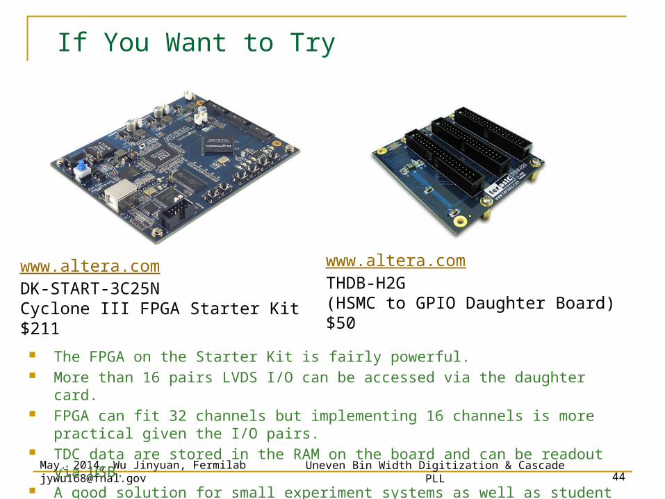
If You Want to Try
The FPGA on the Starter Kit is fairly powerful. More than 16 pairs LVDS I/O can be accessed via the daughter card. FPGA can fit 32 channels but implementing 16 channels is more practical given the I/O pairs. TDC data are stored in the RAM on the board and can be readout via USB. A good solution for small experiment systems as well as student labs.
www.altera.comDK-START-3C25NCyclone III FPGA Starter Kit$211
www.altera.comTHDB-H2G (HSMC to GPIO Daughter Board)$50

Timing Uncertainty Confinement
May. 2014, Wu Jinyuan, Fermilab [email protected] Uneven Bin Width Digitization & Cascade PLL 45

46
Historical Implementation in ASIC TDC
May. 2014, Wu Jinyuan, Fermilab [email protected] Uneven Bin Width Digitization & Cascade PLL
DLL Clock Chain
Encoder
CoarseTime
Counter
HIT CoarseTime
Register
CoarseTime
SelectionLogic
c1c0
HIT is used as CK input which creates unnecessary challenges.
Deadtime is unavoidable. Coarse time recording needs special care. Two array + encoder sets are needed for raising edge and falling edge. The register array must be reset for next event. The encoder must be re-synchronized with system clock in order to interface with readout stage.
Unnecessary Challenges = Extra Efforts + Reduced Performance

47
Unnecessary Challenges
May. 2014, Wu Jinyuan, Fermilab [email protected] Uneven Bin Width Digitization & Cascade PLL
In history, Gray code counters, double counters and dual registers + MUX are found in ASIC TDC coarse time counter schemes.
Theses are unnecessary if the TDC is designed appropriately. In FPGA, a plain binary counter is sufficient.
CoarseTimeCounter
CoarseTimeCounter
CoarseTimeCounter
GrayCodeCounter
000001011010110111101100
Unnecessary for FPGA TDC

48
A Better Implementation
May. 2014, Wu Jinyuan, Fermilab [email protected] Uneven Bin Width Digitization & Cascade PLL
DLL Clock Chain
OR + Register
ClockDomainTransfer
DV EG T4..T0
HITMulti-
SamplingRegister
Array
Deadtimeless operation is possible. No special care is needed for coarse time. Both raising and falling edges are digitized with a single array + encoder set. No resetting is needed for the register array. The output is synchronized with the system clock and is ready to interface with readout stage.
CoarseTime
Counter
TC
16-bit Encoder with Registered Outputs 16-bit Encoder with Registered Outputs
HIT is used as D input.
49
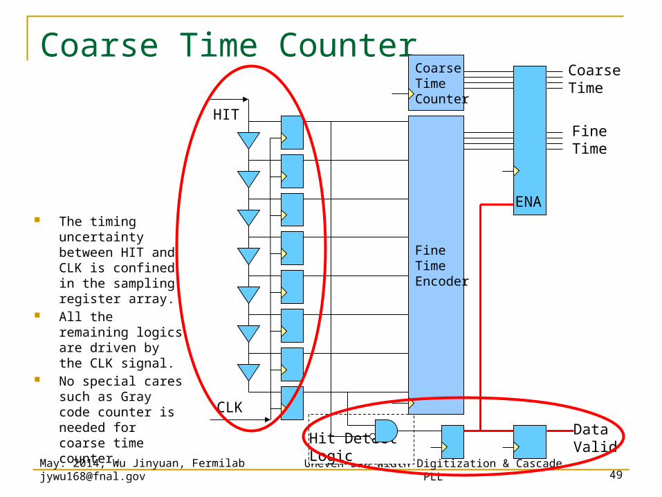
Coarse Time Counter
May. 2014, Wu Jinyuan, Fermilab [email protected] Uneven Bin Width Digitization & Cascade PLL
The timing uncertainty between HIT and CLK is confined in the sampling register array.
All the remaining logics are driven by the CLK signal.
No special cares such as Gray code counter is needed for coarse time counter.
Hit Detect Logic
CoarseTimeCounter
FineTimeEncoder
HIT
CLK
ENA
FineTime
CoarseTime
DataValid

50
Comparison
May. 2014, Wu Jinyuan, Fermilab [email protected] Uneven Bin Width Digitization & Cascade PLL
Historical Scheme:HIT-> CK; (c0..c31)->D;
Preferable Scheme:HIT-> D; (c0..c31)->CK;
Deadtime is unavoidable. Deadtimeless operation is possible.
Coarse time recording needs special care. No special care is needed for coarse time.
Two array + encoder sets are needed for raising edge and falling edge.
Both raising and falling edges are digitized with a single array + encoder set.
The register array must be reset for next event.
No resetting is needed for the register array.
The encoder must be re-synchronized with system clock in order to interface with readout stage.
The output is synchronized with the system clock and is ready to interface with readout stage.

Wave Union?
Photograph: Qi Ji, 2010May. 2014, Wu Jinyuan, Fermilab [email protected] 51Uneven Bin Width Digitization & Cascade PLL

May. 2014, Wu Jinyuan, Fermilab [email protected] Uneven Bin Width Digitization & Cascade PLL 52
Typical Block Diagram
The carry chain and register array captures arrival time of the input transition. The position of the transition is encoded as a time code. Data buffers at various stages are used to store data temporarily. Digitized time data are sent out the chip through data ports.
Carry ChainReg. Array
EncoderBuffer &
LUT
Carry ChainReg. Array
EncoderBuffer &
LUT
Carry ChainReg. Array
EncoderBuffer &
LUT
TDC Channels
OutputBuffer
Parallel-to-Serial
ConverterData

May. 2014, Wu Jinyuan, Fermilab [email protected] Uneven Bin Width Digitization & Cascade PLL 53
Example of an Actual Design of a 16-Channel TDC
The hit time for each of the 16 channel inputs is digitized and encoded. Data from 4 channels are buffered and data from 4 groups of 4 channels are merged together. Raw hit times are converted to fine time through automatic calibration block. Data from all 16 channels are buffered and sent out via 4 pairs of LVDS ports @250 M bits/s.
TDC + Encoder
Data Buffer +Concentration
AutomaticCalibration
OutputBuffer
Serialization

Uneven Bin Width Digitization & Cascade PLL
54May. 2014, Wu Jinyuan, Fermilab [email protected]
TDC Output at Different PS Voltage
0
5
10
15
20
25
1.5 2 2.5
VCCINT (V)
TD
C O
utp
uts
N1
n2
TDC Output at Different PS Voltage
0
5
10
15
20
25
1.5 2 2.5
VCCINT (V)
TD
C O
utp
uts
N1
n2
Tc
Temperature/PS Voltage Effects Power supply voltage
changes from 2.5 V to 1.8 V, (about the same as 100 oC to 0 oC).
Delay speed changes by 30%.
The difference of the two TDC numbers reflects delay speed.
2nd TDC
1st TDC

55
FPGA TDC in Fermilab
May. 2014, Wu Jinyuan, Fermilab [email protected] Uneven Bin Width Digitization & Cascade PLL
The card is a 6U VME board. An Altera Cyclone III FPGA device (EP3C40F484C6) is used to implement TDC. Up to 64 channels can be implemented. A multi-threshold discriminator daughter card can be attached as shown in the right. The project is supported by detector R&D/test beam task codes.

TDC module for SeaQuest. Hardware made in Taiwan. Firmware development efforts:
(0.2 EE + 0.75 Graduate Student)*9 months
1M Gates Actel ProASOC-3 FPGA
TDC in Flash Based FPGA
May. 2014, Wu Jinyuan, Fermilab [email protected] 56Uneven Bin Width Digitization & Cascade PLL
From Su-Yin Wang’s slides

Uneven Bin Width Digitization & Cascade PLL 57May. 2014, Wu Jinyuan, Fermilab [email protected]
FPGA TDC: a Single Chip Solution
TDC FPGA
TDC
FPGA
TDCTDCTDC
DAQ
VTH
In
In
• In modern HEP system, a lot of time it is necessary to put an FPGA after a TDC to handle the generated data.
• It is convenient to include TDC function inside the FPGA.

May. 2014, Wu Jinyuan, Fermilab [email protected] Uneven Bin Width Digitization & Cascade PLL 58
Digitization with Non-uniform Bin Widths
The phenomenon of digitizers with non-uniform bin widths sometimes is called differential non-linearity, which sounds a bad thing.
In fact, digitizers with non-uniform bin widths make precise measurements as long as it is calibrated to the centers of the bins.
A equivalent bin width can be defined as above. The calibration can be done offline or/and online.
L
ww i
i
ieq 12
22 12eqeqw

May. 2014, Wu Jinyuan, Fermilab [email protected] Uneven Bin Width Digitization & Cascade PLL 59
Histogram Booking
The phenomenon of digitizers with non-uniform bin widths sometimes is called differential

May. 2014, Wu Jinyuan, Fermilab [email protected] Uneven Bin Width Digitization & Cascade PLL 60
Summing
The phenomenon of digitizers with non-uniform bin widths sometimes is called differential
1
02
n
kk
nn w
wt