Embed Size (px)
Citation preview
2-1
Topi
c 2
Understanding Noise-Spreading Techniques and their Effects in Switch-Mode Power Applications
John Rice, Dirk Gehrke, and Mike Segal
AbstrAct
A down side to all the benefits of switch-mode power supply (SMPS) power conversion is the potential for noise generation from the high dv/dt and di/dt of the power pulses. When the many techniques for mitigating the generation of EMI fail to provide the necessary noise margin, the application of spread-spectrum frequency dithering (SSFD) may provide a solution. This topic explores modulation techniques, models the behavior in SPICE, and examines real-world behavior in two practical examples.
I. IntroductIon
A switch-mode power supply (SMPS*) offers many advantages over its linear counterpart, including higher efficiency, smaller size and weight, and the ability to boost output voltage above input voltage. With these benefits comes a major drawback—noise. Since switchers generate high dv/dt and di/dt by their very nature, interference with nearby circuits, devices, or systems is possible. Many techniques may be employed to mitigate noise, either at the source or beyond. Of course, it’s best to address noise at the source wherever possible. Common techniques to do so include slowing switching transitions, choosing switching frequency to least disturb the system, snubbing high dv/dt nodes, minimizing high di/dt current loop areas, etc. When common techniques to mitigate noise fail to provide the necessary margin against required limits for a given application, a technique called spread-spectrum frequency dithering (SSFD) may be implemented, whereby the switching frequency is swept within a limited range about a nominal set point. While not suitable for all applications, SSFD is a handy technique for power designers to include in their tool kit.
This topic uses FM theory and SPICE simulations to clarify and quantify the effect of SSFD. We then examine conducted and radiated noise in real-world applications. For conducted noise, the featured application is off-line power-factor correction (PFC). For radiated noise, the featured application is automotive DC/DC
conversion. This topic explores whether these applications might benefit from SSFD, and examines experimental results.
II. QuAntIfyIng the sMPs noIse ProbleM
Electromagnetic compatibility (EMC) is achieved when electronic devices operate normally in their intended environment without conducting or radiating excessive amounts of electromagnetic energy or being susceptible to such energy from internal or external sources.
Electromagnetic interference (EMI) is caused by undesirable radiated electromagnetic fields or conducted voltages and currents. The interference is produced by a source (“aggressor”) and is detected by a “victim” via a coupling path. The coupling path may involve one or more of the following coupling mechanisms:
Common impedance coupling (electric •current)—Conducted noise is coupled between components through interconnecting wires. Common impedance coupling is caused when currents from two or more circuits flow through the same impedance path, such as in a power-supply source and its return wires. Capacitive Coupling (electric field)• —Electric-field coupling is caused by a voltage difference between conductors; the coupling mechanism may be modeled by a capacitor. Inductive Coupling (magnetic field)• —Magnetic-field coupling is caused by current flow in conductors and mutual inductance between the conductors.
*See Appendix B for definitions of acronyms used in this topic.
2-2
Topi
c 2
Radiation (electromagnetic field)• —In a switch-mode power converter, conductors and conductive paths within the circuit carry high-frequency components that act as antennas capable of transmitting radiated electromagnetic energy.
The extent by which an electronic device acts as an EMC aggressor is highly influenced by the frequency at which the converter operates and the magnitude of the voltages and currents associated with its operation. Strict regulations attempt to ensure compatibility between electronic devices by limiting both radiated and conducted emissions at the source.
III. noIse-MItIgAtIon fundAMentAls
There is no shortage of material explaining theoretically and practically the origin and solutions for radiated and conducted EMI in switch-mode power converters, nor is there a shortage of opinion on the subject. Consequently, we must stress that unless the long established fundamentals of power-supply design are applied, no measure of noise spreading will help to achieve the desired result of EMC.
The most common methods of noise reduction include careful component selection, PCB layout, shielding, grounding, input/output filtering, isolation, component separation, and cable design. These can be effectively applied only through an
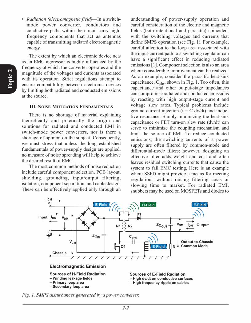
understanding of power-supply operation and careful consideration of the electric and magnetic fields (both intentional and parasitic) coincident with the switching voltages and currents that define SMPS operation (see Fig. 1). For example, careful attention to the loop area associated with the input-current path to a switching regulator can have a significant effect in reducing radiated emissions [1]. Component selection is also an area where considerable improvement can be realized. As an example, consider the parasitic heat-sink capacitance, Cphs, shown in Fig. 1. Too often, this capacitance and other output-stage impedances can compromise radiated and conducted emissions by reacting with high output-stage current and voltage slew rates. Typical problems include ground-current injection (i = C dv/dt) and induc-tive resonance. Simply minimizing the heat-sink capacitance or FET turn-on slew rate (dv/dt) can serve to minimize the coupling mechanism and limit the source of EMI. To reduce conducted emissions, the switching currents of a power supply are often filtered by common-mode and differential-mode filters; however, designing an effective filter adds weight and cost and often leaves residual switching currents that cause the system to fail EMC testing. Here is an example where SSFD might provide a means for meeting regulations without raising filtering costs or slowing time to market. For radiated EMI, snubbers may be used on MOSFETs and diodes to
Fig. 1. SMPS disturbances generated by a power converter.
N1 N2
Q1
Cphs
D1
N
VDM
VCM
VDM
Chassis
Electromagnetic Emission
Input IDM
IDM
ICM2
ICM2
E-Field
E-FieldE-Field H-Field
Sources of E-Field Radiation– High dv/dt on conductive surfaces– High frequency ripple on cables
Output
Output-to-ChassisCommon Mode
ZCOUT
ZCIN
Sources of H-Field Radiation– Winding leakage fields– Primary loop area– Secondary loop area
2-3
Topi
c 2
slow rise and fall times of switching waveforms, to shape the spectral content, and to satisfy regulatory standards. Snubbers can effectively dissipate parasitic resonant energy that could otherwise be radiated, but they also serve to increase switching losses and reduce the efficiency of the power supply, thus compromising another critical consideration for today’s power converters.
If these well established techniques fail to provide sufficient noise margin, only then does it makes sense to investigate the technique of harmonic-peak reduction using SSFD.
IV. QuAntIfyIng eMIssIons
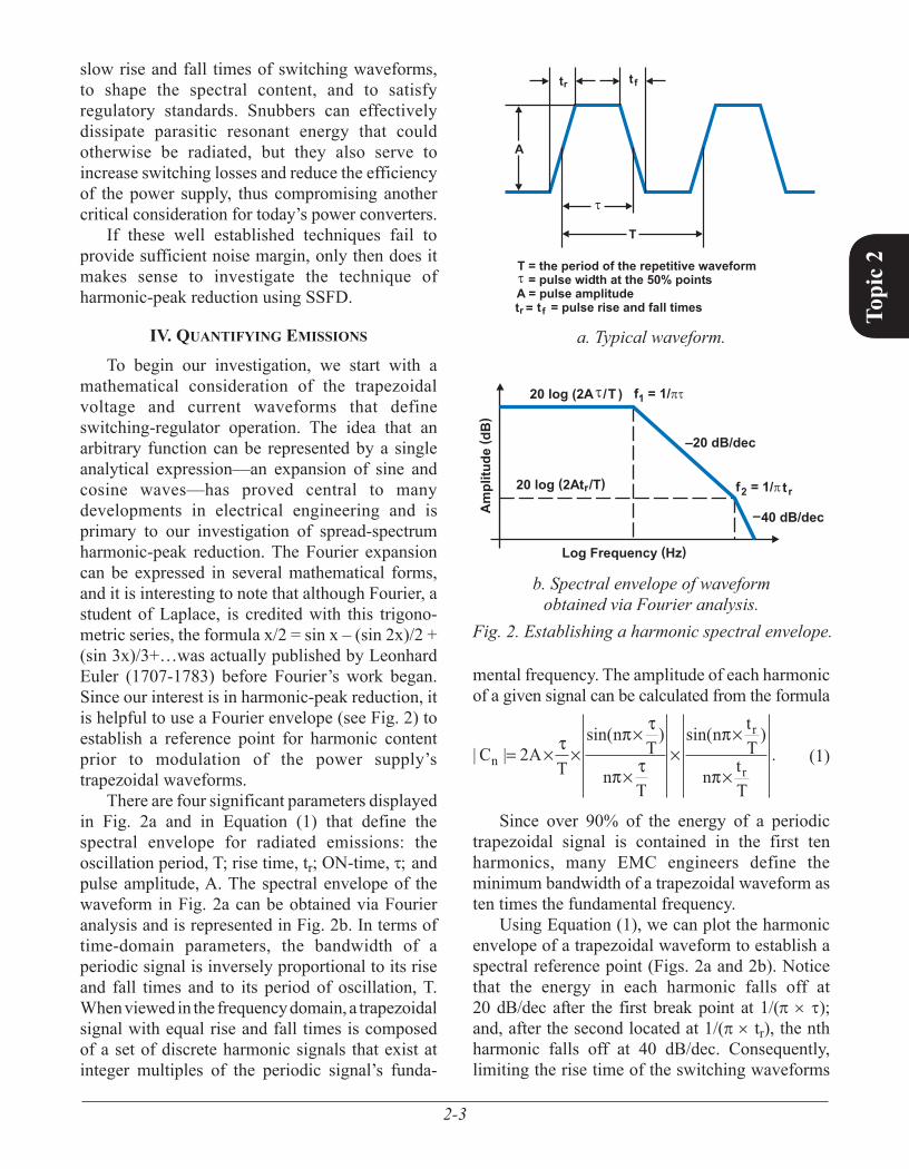
To begin our investigation, we start with a mathematical consideration of the trapezoidal voltage and current waveforms that define switching-regulator operation. The idea that an arbitrary function can be represented by a single analytical expression—an expansion of sine and cosine waves—has proved central to many developments in electrical engineering and is primary to our investigation of spread-spectrum harmonic-peak reduction. The Fourier expansion can be expressed in several mathematical forms, and it is interesting to note that although Fourier, a student of Laplace, is credited with this trigono-metric series, the formula x/2 = sin x – (sin 2x)/2 + (sin 3x)/3+…was actually published by Leonhard Euler (1707-1783) before Fourier’s work began. Since our interest is in harmonic-peak reduction, it is helpful to use a Fourier envelope (see Fig. 2) to establish a reference point for harmonic content prior to modulation of the power supply’s trapezoidal waveforms.
There are four significant parameters displayed in Fig. 2a and in Equation (1) that define the spectral envelope for radiated emissions: the oscillation period, T; rise time, tr; ON-time, τ; and pulse amplitude, A. The spectral envelope of the waveform in Fig. 2a can be obtained via Fourier analysis and is represented in Fig. 2b. In terms of time-domain parameters, the bandwidth of a periodic signal is inversely proportional to its rise and fall times and to its period of oscillation, T. When viewed in the frequency domain, a trapezoidal signal with equal rise and fall times is composed of a set of discrete harmonic signals that exist at integer multiples of the periodic signal’s funda-
mental frequency. The amplitude of each harmonic of a given signal can be calculated from the formula
| |sin( ) sin( )
.C AT
nT
nT
n tT
n tT
n
r
r= 2 × ×
×
××
×
×
τ π τ
π τ
π
π (1)
Since over 90% of the energy of a periodic trapezoidal signal is contained in the first ten harmonics, many EMC engineers define the minimum bandwidth of a trapezoidal waveform as ten times the fundamental frequency.
Using Equation (1), we can plot the harmonic envelope of a trapezoidal waveform to establish a spectral reference point (Figs. 2a and 2b). Notice that the energy in each harmonic falls off at 20 dB/dec after the first break point at 1/(π × τ); and, after the second located at 1/(π × tr), the nth harmonic falls off at 40 dB/dec. Consequently, limiting the rise time of the switching waveforms
a. Typical waveform.
b. Spectral envelope of waveform obtained via Fourier analysis.
Fig. 2. Establishing a harmonic spectral envelope.
A
T
tr t f
T = the period of the repetitive waveformT = pulse width at the 50% pointsA = pulse amplitude
= pulse rise and fall timest = tr f
Am
plitu
de( d
B)
20 log (2A )/T
20 log (2A /T)tr
–20 dB/dec
Log Frequency (Hz)
–40 dB/dec
f = 1/1
f = 1/2 t r
2-4
Topi
c 2
can be effective in attenuating high-frequency harmonic content. The technique for predicting radiated emissions is given in greater mathematical detail in Reference [2].
V. MeAsurIng eMIssIons
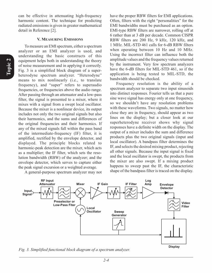
To measure an EMI spectrum, either a spectrum analyzer or an EMI analyzer is used, and understanding the basic constructs of this equipment helps both in understanding the theory of noise measurement and in applying it correctly. Fig. 3 is a simplified block diagram of a super-hetero dyne spectrum analyzer. “Heterodyne” means to mix nonlinearly (i.e., to translate frequency), and “super” refers to superaudio frequencies, or frequencies above the audio range. After passing through an attenuator and a low-pass filter, the signal is presented to a mixer, where it mixes with a signal from a swept local oscillator. Because the mixer is a nonlinear device, its output includes not only the two original signals but also their harmonics, and the sums and differences of the original frequencies and their harmonics. If any of the mixed signals fall within the pass band of the intermediate-frequency (IF) filter, it is amplified, rectified by the envelope detector, and displayed. The principle blocks related to harmonic-peak detection are the mixer, which acts as a multiplier; the IF filter, which sets the reso-lution bandwidth (RBW) of the analyzer; and the envelope detector, which serves to capture either the peak signal excursion or a weighted average.
A general-purpose spectrum analyzer may not
have the proper RBW filters for EMI applications. Often, filters with the right “personalities” for the EMI bandwidths must be purchased as an option. EMI-type RBW filters are narrower, rolling off at 6 rather than at 3 dB per decade. Common CISPR RBW filters are 200 Hz, 9 kHz, 120 kHz, and 1 MHz. MIL-STD 461 calls for 6-dB RBW filters when operating between 10 Hz and 10 MHz. Using the incorrect filter can influence both the amplitude values and the frequency values returned by the instrument. Very few spectrum analyzers have the 6-dB filters for MIL-STD 461, so if the application is being tested to MIL-STD, the bandwidth should be checked.
Frequency resolution is the ability of a spectrum analyzer to separate two input sinusoids into distinct responses. Fourier tells us that a pure sine wave signal has energy only at one frequency, so we shouldn’t have any resolution problems with these waveforms. Two signals, no matter how close they are in frequency, should appear as two lines on the display; but a closer look at our superheterodyne receiver shows why signal responses have a definite width on the display. The output of a mixer includes the sum and difference products plus the two original signals (input and local oscillator). A bandpass filter determines the IF, and selects the desired mixing product, rejecting all other signals. Because the input signal is fixed and the local oscillator is swept, the products from the mixer are also swept. If a mixing product happens to sweep past the IF, the characteristic shape of the bandpass filter is traced on the display.
Fig. 3. Simplified functional block diagram of a spectrum analyzer.
RF InputAttenuator
Preselector orLow-Pass Fiter
SweepGenerator
LocalOscillator
VideoFilter
InputSignal
EnvelopeDetector
LogAmpMixer IF Gain
Display
IF Filter
2-5
Topi
c 2
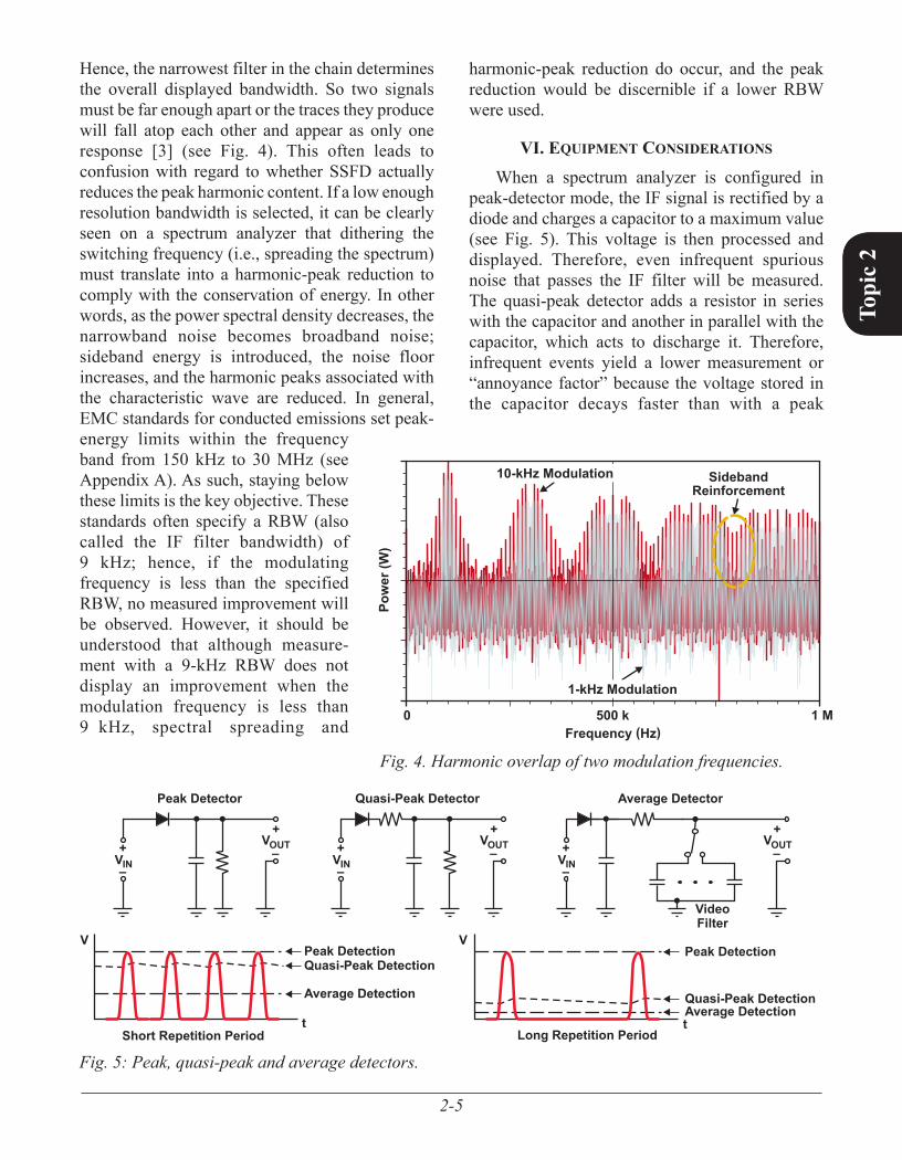
Hence, the narrowest filter in the chain determines the overall displayed bandwidth. So two signals must be far enough apart or the traces they produce will fall atop each other and appear as only one response [3] (see Fig. 4). This often leads to confusion with regard to whether SSFD actually reduces the peak harmonic content. If a low enough resolution bandwidth is selected, it can be clearly seen on a spectrum analyzer that dithering the switching frequency (i.e., spreading the spectrum) must translate into a harmonic-peak reduction to comply with the conservation of energy. In other words, as the power spectral density decreases, the narrowband noise becomes broadband noise; sideband energy is introduced, the noise floor increases, and the harmonic peaks associated with the characteristic wave are reduced. In general, EMC standards for conducted emissions set peak-energy limits within the frequency band from 150 kHz to 30 MHz (see Appendix A). As such, staying below these limits is the key objective. These standards often specify a RBW (also called the IF filter bandwidth) of 9 kHz; hence, if the modulating frequency is less than the specified RBW, no measured improvement will be observed. However, it should be understood that although measure-ment with a 9-kHz RBW does not display an improve ment when the modulation frequency is less than 9 kHz, spectral spreading and
harmonic-peak reduction do occur, and the peak reduction would be discernible if a lower RBW were used.
VI. eQuIPMent consIderAtIons
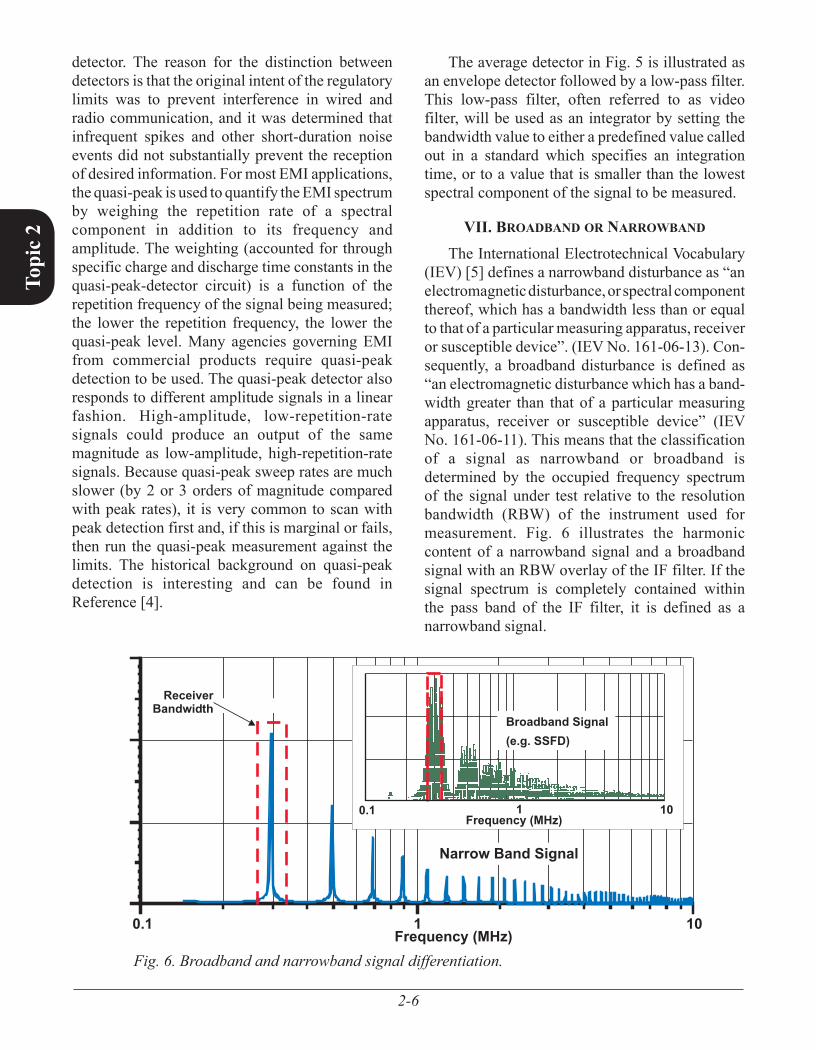
When a spectrum analyzer is configured in peak-detector mode, the IF signal is rectified by a diode and charges a capacitor to a maximum value (see Fig. 5). This voltage is then processed and displayed. Therefore, even infrequent spurious noise that passes the IF filter will be measured. The quasi-peak detector adds a resistor in series with the capacitor and another in parallel with the capacitor, which acts to discharge it. Therefore, infrequent events yield a lower measurement or “annoyance factor” because the voltage stored in the capacitor decays faster than with a peak
T
0 500 k 1 MFrequency (Hz)
Pow
er(W
)
SidebandReinforcement
10-kHz Modulation
1-kHz Modulation
Peak Detector Average Detector
VideoFilter
Quasi-Peak Detector
VIN VINVIN
VOUT VOUT VOUT+ +++ ++
– ––– ––
Short Repetition Period
V
t
Peak Detection
Average Detection
Quasi-Peak Detection
Long Repetition Period
V
t
Peak Detection
Average DetectionQuasi-Peak Detection
Fig. 4. Harmonic overlap of two modulation frequencies.
Fig. 5: Peak, quasi-peak and average detectors.
2-6
Topi
c 2
detector. The reason for the distinction between detectors is that the original intent of the regulatory limits was to prevent interference in wired and radio communication, and it was determined that infrequent spikes and other short-duration noise events did not substantially prevent the reception of desired information. For most EMI applications, the quasi-peak is used to quantify the EMI spectrum by weighing the repetition rate of a spectral component in addition to its frequency and amplitude. The weighting (accounted for through specific charge and discharge time constants in the quasi-peak-detector circuit) is a function of the repetition frequency of the signal being measured; the lower the repetition frequency, the lower the quasi-peak level. Many agencies governing EMI from commercial products require quasi-peak detection to be used. The quasi-peak detector also responds to different amplitude signals in a linear fashion. High-amplitude, low-repetition-rate signals could produce an output of the same magnitude as low-amplitude, high-repetition-rate signals. Because quasi-peak sweep rates are much slower (by 2 or 3 orders of magnitude compared with peak rates), it is very common to scan with peak detection first and, if this is marginal or fails, then run the quasi-peak measurement against the limits. The historical background on quasi-peak detection is interesting and can be found in Reference [4].
The average detector in Fig. 5 is illustrated as an envelope detector followed by a low-pass filter. This low-pass filter, often referred to as video filter, will be used as an integrator by setting the band width value to either a predefined value called out in a standard which specifies an integration time, or to a value that is smaller than the lowest spectral component of the signal to be measured.
VII. broAdbAnd or nArrowbAnd
The International Electrotechnical Vocabulary (IEV) [5] defines a narrowband disturbance as “an electromagnetic disturbance, or spectral component thereof, which has a bandwidth less than or equal to that of a particular measuring apparatus, receiver or susceptible device”. (IEV No. 161-06-13). Con-sequently, a broadband disturbance is defined as “an electromagnetic disturbance which has a band-width greater than that of a particular measuring apparatus, receiver or susceptible device” (IEV No. 161-06-11). This means that the classification of a signal as narrowband or broadband is determined by the occupied frequency spectrum of the signal under test relative to the resolution bandwidth (RBW) of the instrument used for measurement. Fig. 6 illustrates the harmonic content of a narrowband signal and a broadband signal with an RBW overlay of the IF filter. If the signal spectrum is completely contained within the pass band of the IF filter, it is defined as a narrowband signal.
Fig. 6. Broadband and narrowband signal differentiation.
T
Frequency (MHz)0.1 1 10
ReceiverBandwidth
Narrow Band Signal
Frequency (MHz)0.1 1 10
Broadband Signal(e.g. SSFD)
2-7
Topi
c 2
VIII. clArIfyIng the PrIncIPles of sPreAd-sPectruM ModulAtIon
The first practical conceptualization of the spread-spectrum technique is credited to the late silver-screen actress Hedy Lamarr, who, at the height of her Hollywood career in 1942, patented the “Secret Communication System” along with George Antheil. This frequency-switching system improved radio guidance of torpedoes. The idea was about two decades ahead of its time, as it wasn’t until the invention of the transistor by Jack Kilby of Texas Instruments that the U.S. Navy used the idea in secure military communications. Fifty years later, in 1992, researchers at Virginia Polytechnic in Blacksburg, Virginia, applied the spread-spectrum technique to the power supply as a means of reducing harmonic peaks and spreading noise energy associated with a switch-mode power converter.
Today spread-spectrum technology is used in virtually all high-speed wireless communi-cations—including cell phones and Wi-Fi data-com mu ni cation systems. The technology is also commonly used in high-speed digital-clocking systems to reduce EMI.
IX. eXPlAInIng hArMonIc sPreAdIng wIth fM theory
EMI reduction by frequency modulation of a power supply’s switching frequency can be explored using classical frequency-modulation
(FM) theory as detailed in Reference [6]. Frequency modulation theoretically will produce an infinite number of sidebands; however, the magnitudes of the spectral components of the higher-order sidebands are typically negligible. Given a periodic signal, the emission power will center at the switching frequency and harmonics associated with the waveform duty cycle. At exactly 50% duty cycle, a square wave’s energy is concentrated in the odd harmonics, resulting in a worst-case EMI condition with maximum peak amplitude; but this is generally not the case in a switching power supply. In fact, any deviation from 50% will result in a spreading effect by increasing energy in the even harmonics. Modulating the switching frequency within a limited range creates sidebands (spaced by the modulating frequency) and decreases the spectral density, further lowering the harmonic peaks.
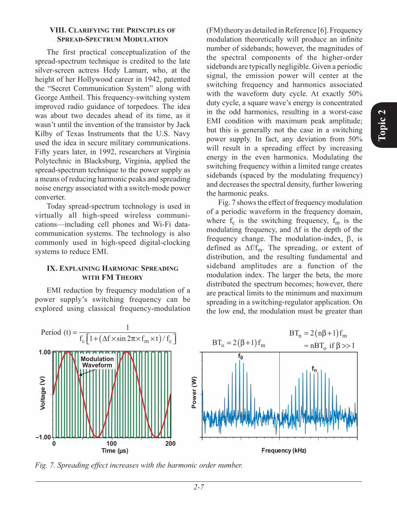
Fig. 7 shows the effect of frequency modulation of a periodic waveform in the frequency domain, where fc is the switching frequency, fm is the modulating frequency, and ∆f is the depth of the frequency change. The modulation-index, β, is defined as ∆f/fm. The spreading, or extent of distribution, and the resulting fundamental and sideband amplitudes are a function of the modulation index. The larger the beta, the more distributed the spectrum becomes; however, there are practical limits to the minimum and maximum spreading in a switching-regulator application. On the low end, the modulation must be greater than
Fig. 7. Spreading effect increases with the harmonic order number.
Frequency (kHz)
Pow
er(W
)
Time (µs)0 100 200
f0fn
Voltage
( V)
–1.00
1.00ModulationWaveform
Periodf f f t fc m c
(t) =+ ( )
11 2∆ × × ×sin /π BT fo m= +( )2 1β
BT n fnBT
n m
o
= +( )≈ >>
2 1ββ if 1
2-8
Topi
c 2
the resolution bandwidth specified in the EMC standard or no improvement will be realized. In addition, the selection of a modulating index, β, with spreading artifacts below 20 kHz, could manifest itself as audible noise. On the high end, one has to take care when the modulating switching frequency is greater than the loop-crossover frequency of the feedback-control loop, as this could impact loop stability and output-ripple voltage.
There are two important characteristics of a frequency-modulated waveform for a continuous modulating frequency, as described by Carson’s bandwidth rule (CBR). The first is that the total power of a signal is unaffected by the frequency modulation. In fact, it is equal to the sum of the squares of each harmonic. The second characteristic is that 98% of the total power of a frequency-modulated signal is contained inside the bandwidth 2(∆f + fm); or in terms of beta, 2(β+1) × fm. Hence the energy of the fundamental component is spread into a band, BT, given by: BT = 2(Δf + fm), whereas subsequent harmonic bandwidth increases with the harmonic order number, n, according to: BTn = 2fm(1+n × Δf/fm). It is thus important to note that as the modulation index increases with each harmonic, so does the scattering effect and the possibility for overlap.
X. ModulAtIon wAVeforMs
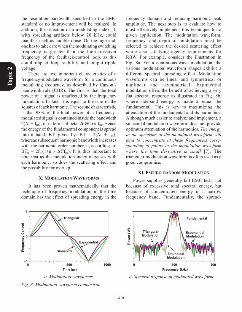
It has been proven mathematically that the technique of frequency modulation in the time domain has the effect of spreading energy in the
frequency domain and reducing harmonic-peak amplitude. The next step is to evaluate how to most effectively implement this technique for a given application. The modulation waveform, frequency, and depth of modulation must be selected to achieve the desired scattering effect while also satisfying agency require ments for RBW. For example, consider the illustration in Fig. 8a. For a continuous-wave modulation, the various modulation waveform shapes exhibit a different spectral spreading effect. Modulation waveforms can be linear and symmetrical or nonlinear and asymmetrical. Exponential modulation offers the benefit of achieving a very flat spectral response as illustrated in Fig. 8b, where sideband energy is made to equal the fundamental. This is key to maximizing the attenuation of the fundamental and its harmonics. Although much easier to analyze and implement, a sinusoidal modulation waveform does not provide optimum attenuation of the harmonics. The energy in the spectrum of the modulated waveform will tend to concentrate at those frequencies corre-sponding to points in the modulation waveform where the time derivative is small [7]. The triangular modulation waveform is often used as a good compromise.
XI. Pseudo-rAndoM ModulAtIon
Power supplies generally fail EMC tests, not because of excessive total spectral energy, but because of concentrated energy in a narrow frequency band. Fundamentally, the spread-
b. Spectral response of modulated waveform.a. Modulation waveforms.Fig. 8. Modulation waveform comparison.
Frequency (kHz)0 100 200
Pow
er(W
)
Time (µs)
FrequencyCon
trol
Exponential
SinusoidalModulation
TriangularModulation
ExponentialModulation
FundamentalTriangular
Sinusoidal
500 10000
0
–1
1
2-9
Topi
c 2
spectrum techniques as applied to power converters involves varying the switching frequency from cycle to cycle, changing the frequency spectrum from a train of large spikes concentrated at the switching frequency and its harmonics to a smoother, more continuous spectrum. Depending on the modulation waveform and the test setup parameters (e.g., RBW of the spectrum analyzer) employed, reduction of the fundamental and harmonics can exceed 15 dB. However, the standards used for EMC measurements and the operation of the EMC equipment must be carefully understood when an effective noise-reduction technique is being qualified. In a spread-spectrum-modulated configuration, the fundamental and each harmonic is swept by the modulation signal. The damping of the harmonic is greatest if the dwell time of the modulated harmonic is much shorter than the settling time of the resolution filter. Since the RBW sets the settling time of the IF filter, the modulation frequency must be significantly higher than the RBW of the spectrum analyzer.
Although the fixed-frequency modulation shown in Fig. 8a is clearly effective in spreading harmonic content, in some cases it may not provide sufficient attenuation of the fundamental. An alternative to fixed-frequency modulation is random or pseudo-random modulation—either of which can actually result in greater spectral spreading of the fundamental. With a pseudo-random noise generator, the switching frequency varies randomly from cycle to cycle over a range determined by the random-number generator’s clock. Each frequency within this range, including
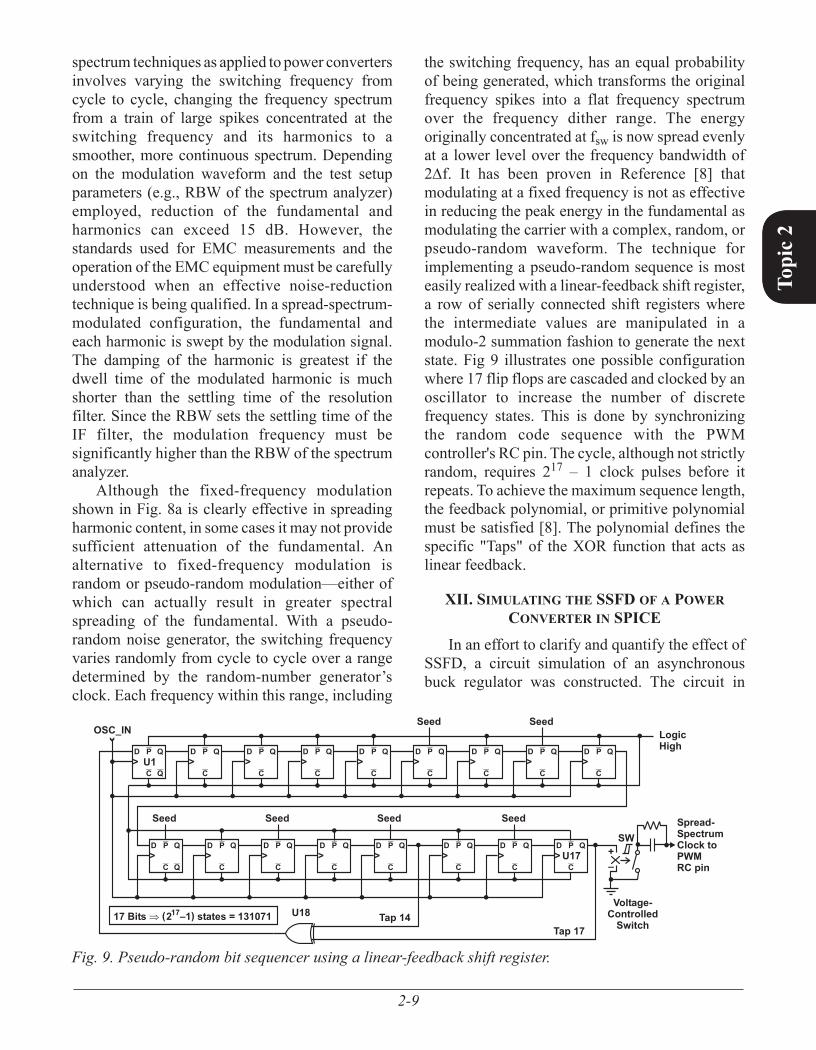
the switching frequency, has an equal probability of being generated, which transforms the original frequency spikes into a flat frequency spectrum over the frequency dither range. The energy originally concentrated at fsw is now spread evenly at a lower level over the frequency bandwidth of 2∆f. It has been proven in Ref er ence [8] that modulating at a fixed frequency is not as effective in reducing the peak energy in the fundamental as modulating the carrier with a complex, random, or pseudo-random waveform. The technique for implementing a pseudo-random sequence is most easily realized with a linear-feedback shift register, a row of serially connected shift registers where the intermediate values are manipulated in a modulo-2 summation fashion to generate the next state. Fig 9 illustrates one possible configuration where 17 flip flops are cascaded and clocked by an oscillator to increase the number of discrete frequency states. This is done by synchronizing the random code sequence with the PWM controller's RC pin. The cycle, although not strictly random, requires 217 – 1 clock pulses before it repeats. To achieve the maximum sequence length, the feedback polynomial, or primitive polynomial must be satisfied [8]. The polynomial defines the specific "Taps" of the XOR function that acts as linear feedback.
XII. sIMulAtIng the ssfd of A Power conVerter In sPIce
In an effort to clarify and quantify the effect of SSFD, a circuit simulation of an asynchronous buck regulator was constructed. The circuit in
Fig. 9. Pseudo-random bit sequencer using a linear-feedback shift register.
Spread-SpectrumClock toPWMRC pin
SW+–
Seed
U18
U1
U17
OSC_IN
17 Bits (2 –1) states = 131071 17 Tap 14Tap 17
Q
D> > > > > > > > >
P Q
C
D P Q
C
D P Q
C
D P Q
C
D P Q
C
D P Q
C
D P Q
C
D P Q
C
D P Q
C
SeedLogicHigh
SeedSeedSeedSeed
Voltage-ControlledSwitch
Q
D> > > > > > > >
P Q
C
D P Q
C
D P Q
C
D P Q
C
D P Q
C
D P Q
C
D P Q
C
D P Q
C
2-10
Topi
c 2
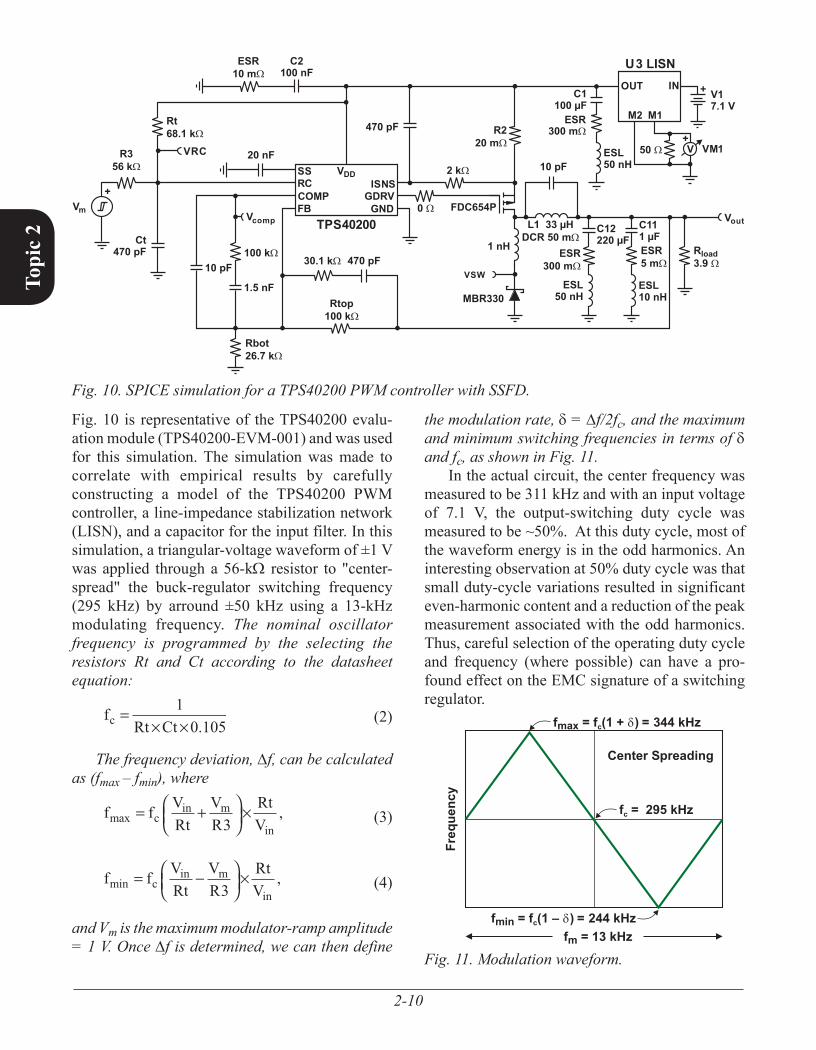
Fig. 10 is representative of the TPS40200 evalu-ation module (TPS40200-EVM-001) and was used for this simulation. The simulation was made to correlate with empirical results by carefully constructing a model of the TPS40200 PWM controller, a line-impedance stabilization network (LISN), and a capacitor for the input filter. In this simulation, a triangular-voltage waveform of ±1 V was applied through a 56-kW resistor to "center-spread" the buck-regulator switching frequency (295 kHz) by arround ±50 kHz using a 13-kHz modulating frequency. The nominal oscillator frequency is programmed by the selecting the resistors Rt and Ct according to the datasheet equation:
fRt Ctc = 1
0 105× × . (2)
The frequency deviation, ∆f, can be calculated as (fmax – fmin), where
f f VRt
VR
RtVc
in m
inmax ,= +
3×
(3)
f f VRt
VR
RtVc
in m
inmin ,= −
3×
(4)
and Vm is the maximum modulator-ramp amplitude = 1 V. Once ∆f is determined, we can then define
the modula tion rate, d = ∆f/2fc, and the maximum and minimum switching frequencies in terms of d and fc, as shown in Fig. 11.
In the actual circuit, the center frequency was measured to be 311 kHz and with an input voltage of 7.1 V, the output-switching duty cycle was measured to be ~50%. At this duty cycle, most of the waveform energy is in the odd harmonics. An interesting observation at 50% duty cycle was that small duty-cycle variations resulted in significant even-harmonic content and a reduction of the peak measurement associated with the odd harmonics. Thus, careful selection of the operating duty cycle and frequency (where possible) can have a pro-found effect on the EMC signature of a switching regulator.
Freq
uenc
y
f = 13 kHzm
Center Spreading
f = 295 kHzc
f = f (1 + ) = 344 kHzmax c
f = f (1 – ) = 244 kHzmin c
Fig. 11. Modulation waveform.
Fig. 10. SPICE simulation for a TPS40200 PWM controller with SSFD.
TPS40200
SSRC
FB
ISNS
INOUT
Vcomp
VRC VM1
FDC654P
10 pF
MBR330
1 nH
ESL50 nH
ESL10 nH
C12220 µF
C111 µF
ESR300 m
ESR5 m
R3.9load
L1 33 µHDCR 50 m
M2
V17.1 V
50
M1
U3 LISN
20 nF
ESR10 m
C2100 nF
470 pF R220 m
2 k
0
100 k
Rbot26.7 k
R356 k
Rtop100 k
470 pF30.1 k
1.5 nF
10 pF
GNDCOMP GDRV
VDD
+
+Rt68.1 k
Ct470 pF
ESL50 nH
C1100 µFESR
300 m
Vm
+
VSW
Vout
V
2-11
Topi
c 2
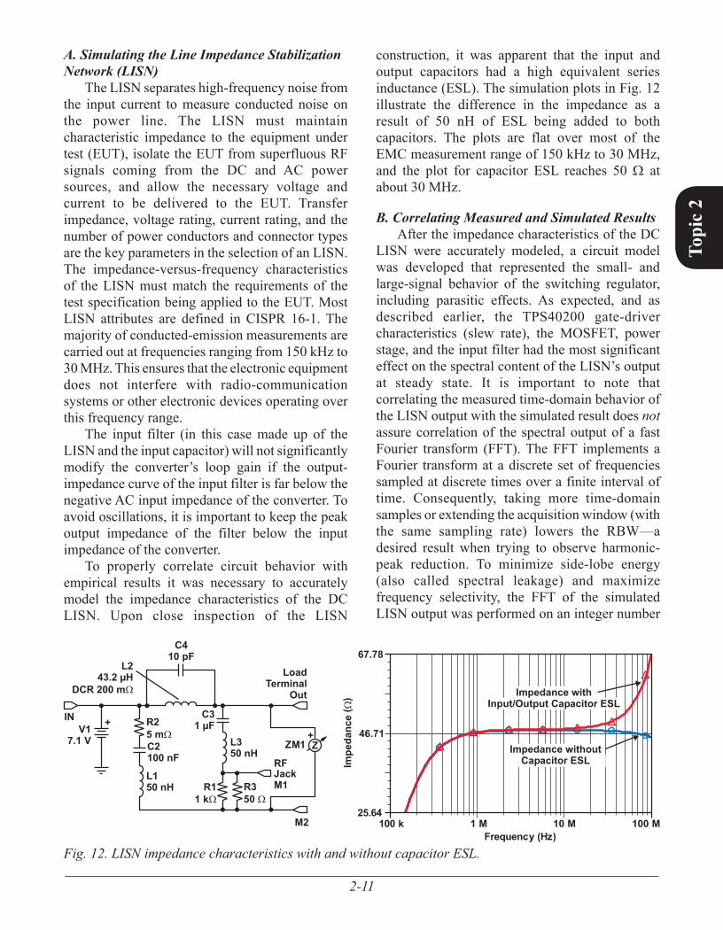
Fig. 12. LISN impedance characteristics with and without capacitor ESL.
M2
+ZM1
T
Frequency (Hz)100 k 1 M 10 M 100 M
25.64
46.71
Impedance()
IN
C410 pF
L150 nH
L350 nH
L243.2 µH
DCR 200 mLoad
TerminalOut
RFJackM1
R25 mV1
7.1 V C2100 nF
R11 k
R350
C31 µF+
Z
67.78
Impedance withoutCapacitor ESL
Impedance withInput/Output Capacitor ESL
A. Simulating the Line Impedance Stabilization Network (LISN)
The LISN separates high-frequency noise from the input current to measure conducted noise on the power line. The LISN must maintain characteristic impedance to the equipment under test (EUT), isolate the EUT from superfluous RF signals coming from the DC and AC power sources, and allow the necessary voltage and current to be delivered to the EUT. Transfer impedance, voltage rating, current rating, and the number of power conductors and connector types are the key parameters in the selection of an LISN. The impedance-versus-frequency characteristics of the LISN must match the requirements of the test specification being applied to the EUT. Most LISN attributes are defined in CISPR 16-1. The majority of conducted-emission measurements are carried out at frequencies ranging from 150 kHz to 30 MHz. This ensures that the electronic equipment does not interfere with radio-communication systems or other electronic devices operating over this frequency range.
The input filter (in this case made up of the LISN and the input capacitor) will not significantly modify the converter’s loop gain if the output-impedance curve of the input filter is far below the negative AC input impedance of the converter. To avoid oscillations, it is important to keep the peak output impedance of the filter below the input impedance of the converter.
To properly correlate circuit behavior with empirical results it was necessary to accurately model the impedance characteristics of the DC LISN. Upon close inspection of the LISN
construction, it was apparent that the input and output capacitors had a high equivalent series inductance (ESL). The simulation plots in Fig. 12 illustrate the difference in the impedance as a result of 50 nH of ESL being added to both capacitors. The plots are flat over most of the EMC measurement range of 150 kHz to 30 MHz, and the plot for capacitor ESL reaches 50 W at about 30 MHz.
B. Correlating Measured and Simulated ResultsAfter the impedance characteristics of the DC
LISN were accurately modeled, a circuit model was developed that represented the small- and large-signal behavior of the switching regulator, including parasitic effects. As expected, and as described earlier, the TPS40200 gate-driver characteristics (slew rate), the MOSFET, power stage, and the input filter had the most significant effect on the spectral content of the LISN’s output at steady state. It is important to note that correlating the measured time-domain behavior of the LISN output with the simulated result does not assure correlation of the spectral output of a fast Fourier transform (FFT). The FFT implements a Fourier transform at a discrete set of frequencies sampled at discrete times over a finite interval of time. Consequently, taking more time-domain samples or extending the acquisition window (with the same sampling rate) lowers the RBW—a desired result when trying to observe harmonic-peak reduction. To minimize side-lobe energy (also called spectral leakage) and maximize frequency selectivity, the FFT of the simulated LISN output was performed on an integer number
2-12
Topi
c 2
of cycles > 30 and at a sample rate of 65536. A rectangular windowing function was applied to shape the time portion of the measurement data. Windowing helps to minimize the edge effect that can occur when a noninteger number of cycles is evaluated, but selecting a window function is not an easy task. Each window function has its own characteristics and suitability for different applications. A detailed tutorial on this subject can be found on the National Instruments Web site at: http://zone.ni.com/devzone/cda/tut/p/id/4186
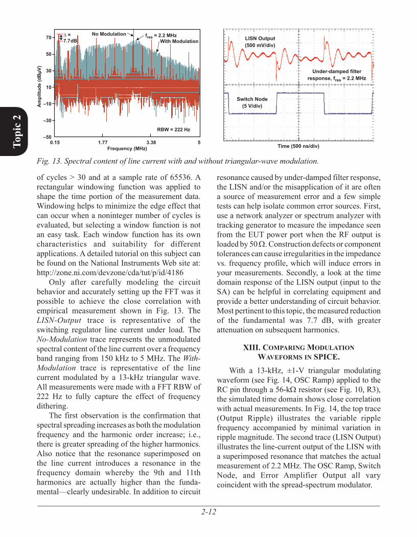
Only after carefully modeling the circuit behavior and accurately setting up the FFT was it possible to achieve the close correlation with empirical measurement shown in Fig. 13. The LISN-Output trace is representative of the switching regulator line current under load. The No-Modulation trace represents the unmodulated spectral content of the line current over a frequency band ranging from 150 kHz to 5 MHz. The With-Modulation trace is representative of the line current modulated by a 13-kHz triangular wave. All measurements were made with a FFT RBW of 222 Hz to fully capture the effect of frequency dithering.
The first observation is the confirmation that spectral spreading increases as both the modulation frequency and the harmonic order increase; i.e., there is greater spreading of the higher harmonics. Also notice that the resonance superimposed on the line current introduces a resonance in the frequency domain whereby the 9th and 11th harmonics are actually higher than the funda-mental—clearly undesirable. In addition to circuit
resonance caused by under-damped filter response, the LISN and/or the misapplication of it are often a source of measurement error and a few simple tests can help isolate common error sources. First, use a network analyzer or spectrum analyzer with tracking generator to measure the impedance seen from the EUT power port when the RF output is loaded by 50 W. Construction defects or component tolerances can cause irregularities in the impedance vs. frequency profile, which will induce errors in your measurements. Secondly, a look at the time domain response of the LISN output (input to the SA) can be helpful in correlating equipment and provide a better understanding of circuit behavior. Most pertinent to this topic, the measured reduction of the fundamental was 7.7 dB, with greater attenuation on subsequent harmonics.
XIII. coMPArIng ModulAtIon wAVeforMs In sPIce.
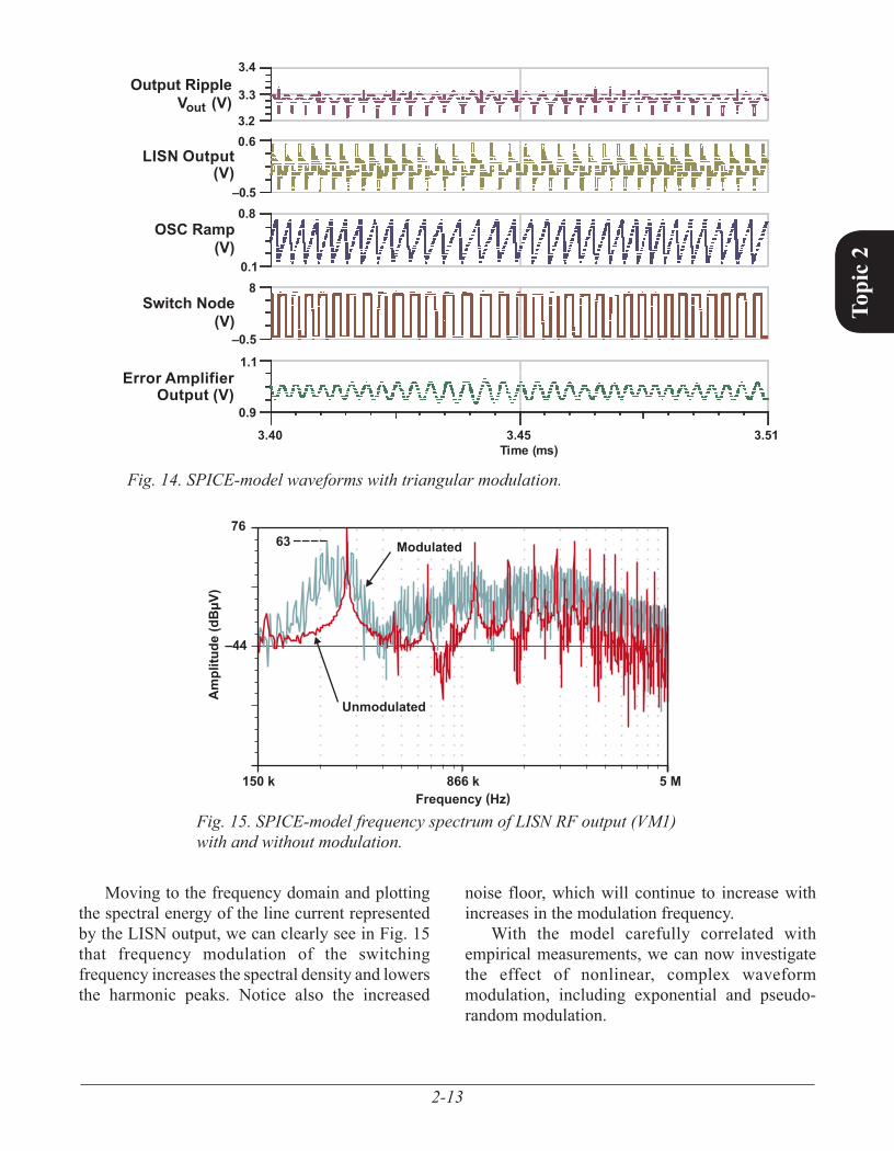
With a 13-kHz, ±1-V triangular modu lating wave form (see Fig. 14, OSC Ramp) applied to the RC pin through a 56-kW resistor (see Fig. 10, R3), the simulated time domain shows close correlation with actual measurements. In Fig. 14, the top trace (Output Ripple) illustrates the variable ripple frequency accompanied by minimal variation in ripple magnitude. The second trace (LISN Output) illustrates the line-current output of the LISN with a superimposed resonance that matches the actual measurement of 2.2 MHz. The OSC Ramp, Switch Node, and Error Amplifier Output all vary coincident with the spread-spectrum modulator.
Fig. 13. Spectral content of line current with and without triangular-wave modulation.Frequency (MHz)
Amplitu
de(dBµV
)
0.15
70
50
30
10
–10
–30
–501.77 3.38 5
No ModulationWith Modulation
f = 2.2 MHzres
RBW = 222 Hz
=7.7dB
Time (500 ns/div)
LISN Output(500 mV/div)
Switch Node(5 V/div)
Under-damped filterresponse, f = 2.2 MHzres
2-13
Topi
c 2
Fig. 14. SPICE-model waveforms with triangular modulation.
Time (ms)3.40 3.45 3.51
Output RippleV (V)out
3.2
3.4
3.3
LISN Output(V)
–0.5
0.6
OSC Ramp(V)
0.1
0.8
Switch Node(V)–0.5
0.9
8
Error AmplifierOutput (V)
1.1
Fig. 15. SPICE-model frequency spectrum of LISN RF output (VM1) with and without modulation.
T 7663
–44
150 k 866 k 5 MFrequency (Hz)
Amplitude
(dBµV)
Modulated
Unmodulated
Moving to the frequency domain and plotting the spectral energy of the line current represented by the LISN output, we can clearly see in Fig. 15 that frequency modulation of the switching frequency increases the spectral density and lowers the harmonic peaks. Notice also the increased
noise floor, which will continue to increase with increases in the modulation frequency.
With the model carefully correlated with empirical measurements, we can now investigate the effect of nonlinear, complex waveform modulation, including exponential and pseudo-random modulation.
2-14
Topi
c 2
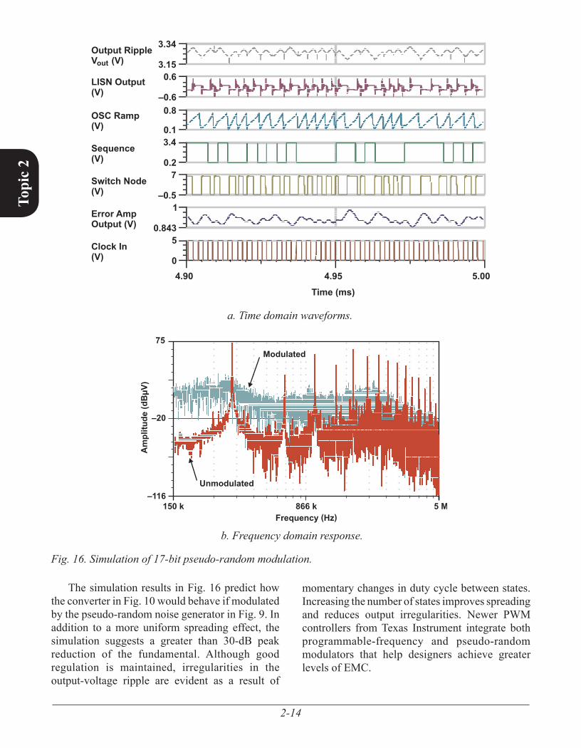
The simulation results in Fig. 16 predict how the converter in Fig. 10 would behave if modulated by the pseudo-random noise generator in Fig. 9. In addition to a more uniform spreading effect, the simulation suggests a greater than 30-dB peak reduction of the fundamental. Although good regulation is maintained, irregularities in the output-voltage ripple are evident as a result of
momentary changes in duty cycle between states. Increasing the number of states improves spreading and reduces output irregularities. Newer PWM controllers from Texas Instrument integrate both programmable-frequency and pseudo-random modulators that help designers achieve greater levels of EMC.
Fig. 16. Simulation of 17-bit pseudo-random modulation.
Time (ms)4.90 4.95 5.00
Output RippleV (V)out 3.15
3.34
LISN Output(V) –0.6
0.6
OSC Ramp(V) 0.1
0.8
Sequence(V) 0.2
3.4
Switch Node(V) –0.5
7
Error AmpOutput (V) 0.843
1
Clock In(V) 0
5
T 75
–20
–116150 k 866 k 5 M
Frequency (Hz)
Amplitu
de(dBµV
)
Modulated
Unmodulated
b. Frequency domain response.
a. Time domain waveforms.
2-15
Topi
c 2
XIV. conducted-eMIssIons eXAMPle: Power-fActor correctIon (Pfc)
This section and section XV examine using SSFD in PFC and automotive DC/DC applications. Included are conducted and radiated EMI measurements to evaluate the impact of using SSFD.
A. What is PFC?The power factor (PF) is the ratio of real power
(watts) to apparent power (volt-amperes) in an AC circuit.
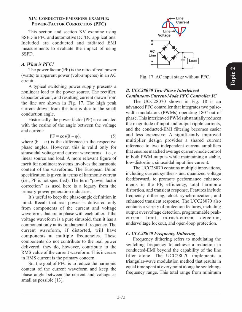
A typical switching power supply presents a nonlinear load to the power source. The rectifier, capacitor circuit, and resulting current drawn from the line are shown in Fig. 17. The high peak current drawn from the line is due to the small conduction angle.
Historically, the power factor (PF) is calculated with the cosine of the angle between the voltage and current:
PF = cos(θ – ϕ), (5)where (θ – ϕ) is the difference in the respective phase angles. However, this is valid only for sinusoidal voltage and current waveforms—i.e., a linear source and load. A more relevant figure of merit for nonlinear systems involves the harmonic content of the waveforms. The European Union specification is given in terms of harmonic current (i.e., PF is not specified). The term “power-factor correction” as used here is a legacy from the primary-power generation industries.
It’s useful to keep the phase-angle definition in mind. Recall that real power is delivered only from components of the current and voltage waveforms that are in phase with each other. If the voltage waveform is a pure sinusoid, then it has a component only at its fundamental frequency. The current waveform, if distorted, will have components at multiple frequencies. These components do not contribute to the real power delivered; they do, however, contribute to the RMS value of the current waveform. This increase in RMS current is the primary concern.
So, the goal of PFC is to reduce the harmonic content of the current waveform and keep the phase angle between the current and voltage as small as possible [13].
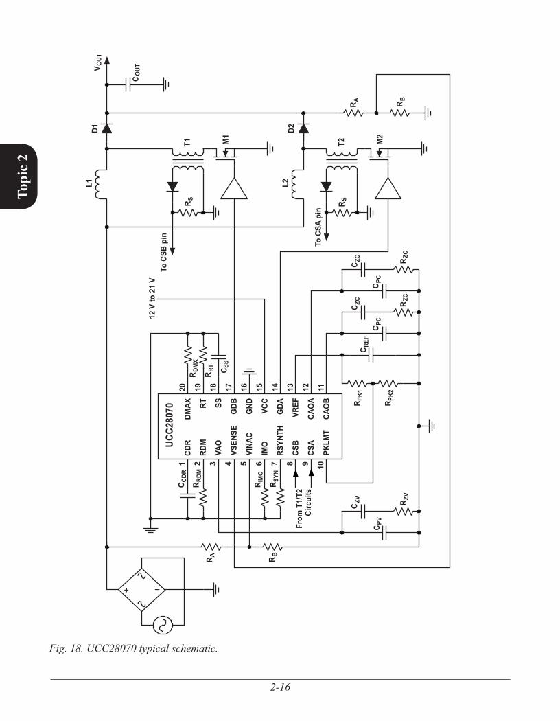
B. UCC28070 Two-Phase Interleaved Continuous-Current-Mode PFC Controller IC
The UCC28070 shown in Fig. 18 is an advanced PFC controller that integrates two pulse-width modulators (PWMs) operating 180° out of phase. This interleaved PWM substantially reduces the magnitude of input and output ripple currents, and the conducted-EMI filtering becomes easier and less expensive. A significantly improved multiplier design provides a shared current reference to two independent current amplifiers that ensures matched average current-mode control in both PWM outputs while maintaining a stable, low-distortion, sinusoidal input line current.
The UCC28070 contains multiple innovations, including current synthesis and quantized voltage feedforward, to promote performance enhance-ments in the PF, efficiency, total harmonic distortion, and transient response. Features includ e frequency dithering, clock synchronization, and enhanced transient response. The UCC28070 also contains a variety of protection features, including output overvoltage detection, programmable peak-current limit, in-rush-current detection, undervoltage lockout, and open-loop protection.
C. UCC28070 Frequency Dithering Frequency dithering refers to modulating the
switching frequency to achieve a reduction in conducted-EMI beyond the capability of the line filter alone. The UCC28070 implements a triangular-wave modulation method that results in equal time spent at every point along the switching-frequency range. This total range from minimum
LineCurrent
LineVoltage
ACLine
Load+
Fig. 17. AC input stage without PFC.
2-16
Topi
c 2
Fig. 18. UCC28070 typical schematic.
+ –
V OUT
12V
to21
V
M2
RB
R A RB
M1
L2D2D1
CO
UT
R A
C PC
C PC
C ZC
C ZC
RZC
RZC
C SS
R RDM
R RT
T1 T2
C CDR
R DM
X
R SYN
C REF
R PK1
R PK2
CZV R Z
V
C PV
R S RS
1 2 3 4 5 6 7 8 9 10
20 19 18 17 16 15 14 13 12 11CA
OA
CAO
BPK
LMT
GND
VAO
VINA
C
VSEN
SE
CSA
CSB
RT
CDR
SS
GDB
GDA
IMO
VCC
RSYN
TH
VREF
DMAX
RDM
R IM
O
ToCS
Bpi
n
ToCS
Api
n
From
T1/T
2Ci
rcui
ts
L1
UCC2
8070
2-17
Topi
c 2
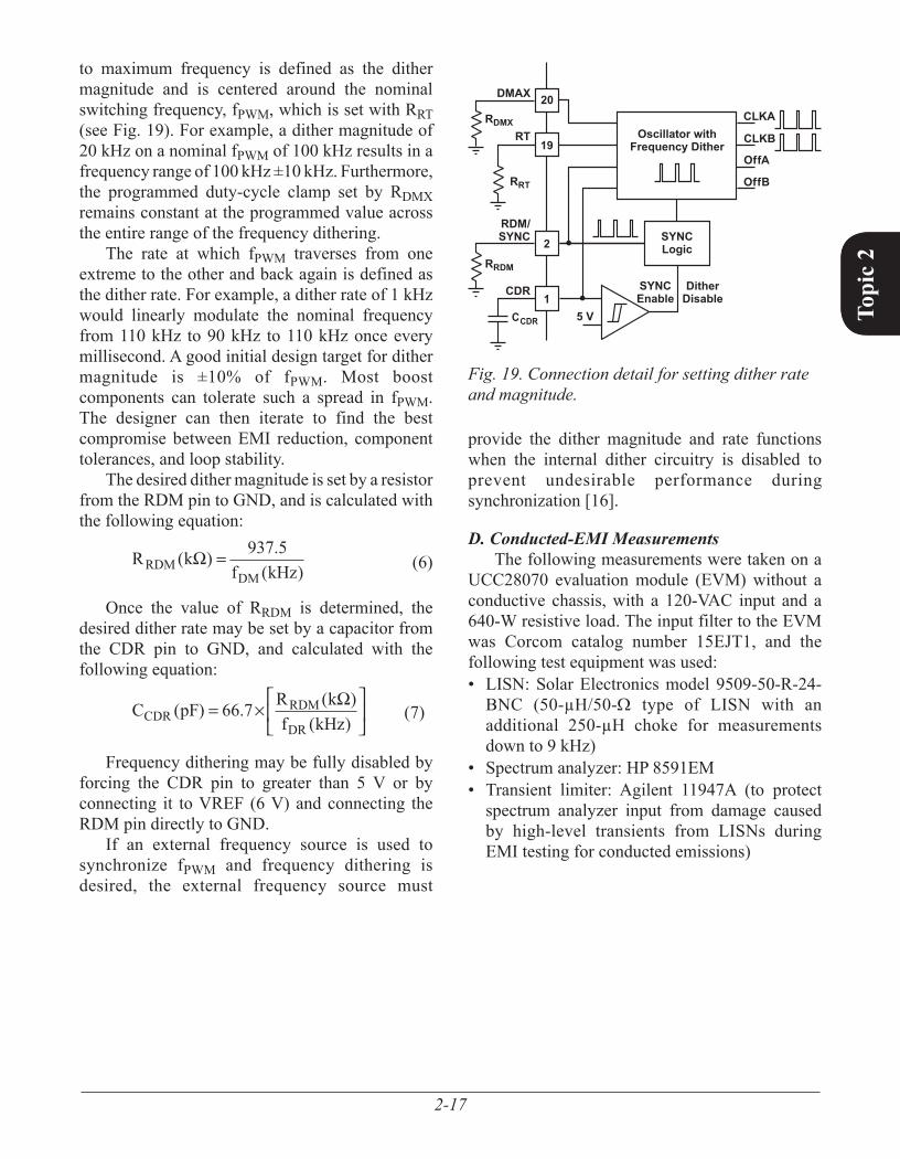
to maximum frequency is defined as the dither magnitude and is centered around the nominal switching frequency, fPWM, which is set with RRT (see Fig. 19). For example, a dither magnitude of 20 kHz on a nominal fPWM of 100 kHz results in a frequency range of 100 kHz ±10 kHz. Furthermore, the programmed duty-cycle clamp set by RDMX remains constant at the programmed value across the entire range of the frequency dithering.
The rate at which fPWM traverses from one extreme to the other and back again is defined as the dither rate. For example, a dither rate of 1 kHz would linearly modulate the nominal frequency from 110 kHz to 90 kHz to 110 kHz once every millisecond. A good initial design target for dither magnitude is ±10% of fPWM. Most boost components can tolerate such a spread in fPWM. The designer can then iterate to find the best compromise between EMI reduction, component tolerances, and loop stability.
The desired dither magnitude is set by a resistor from the RDM pin to GND, and is calculated with the following equation:
R k
f kHzRDMDM
( ) .( )
Ω = 937 5
(6)
Once the value of RRDM is determined, the desired dither rate may be set by a capacitor from the CDR pin to GND, and calculated with the following equation:
C pF R k
f kHzCDRRDM
DR( ) . ( )
( )=
66 7× Ω
(7)
Frequency dithering may be fully disabled by forcing the CDR pin to greater than 5 V or by connecting it to VREF (6 V) and connecting the RDM pin directly to GND.
If an external frequency source is used to synchronize fPWM and frequency dithering is desired, the external frequency source must
provide the dither magnitude and rate functions when the internal dither circuitry is disabled to prevent undesirable performance during synchronization [16].
D. Conducted-EMI MeasurementsThe following measurements were taken on a
UCC28070 evaluation module (EVM) without a conductive chassis, with a 120-VAC input and a 640-W resistive load. The input filter to the EVM was Corcom catalog number 15EJT1, and the following test equipment was used:
LISN: Solar Electronics model 9509-50-R-24-• BNC (50-µH/50-W type of LISN with an additional 250-µH choke for measurements down to 9 kHz)Spectrum analyzer: HP 8591EM• Transient limiter: Agilent 11947A (to protect • spectrum analyzer input from damage caused by high-level transients from LISNs during EMI testing for conducted emissions)
Fig. 19. Connection detail for setting dither rate and magnitude.
DMAX
CLKA
CLKB
OffA
OffB
RT
RRT
RDMX
RRDM
CDR1
2
19
20
Oscillator withFrequency Dither
SYNCLogic
SYNCEnable
5 V+
–
DitherDisable
RDM/SYNC
CCDR
2-18
Topi
c 2
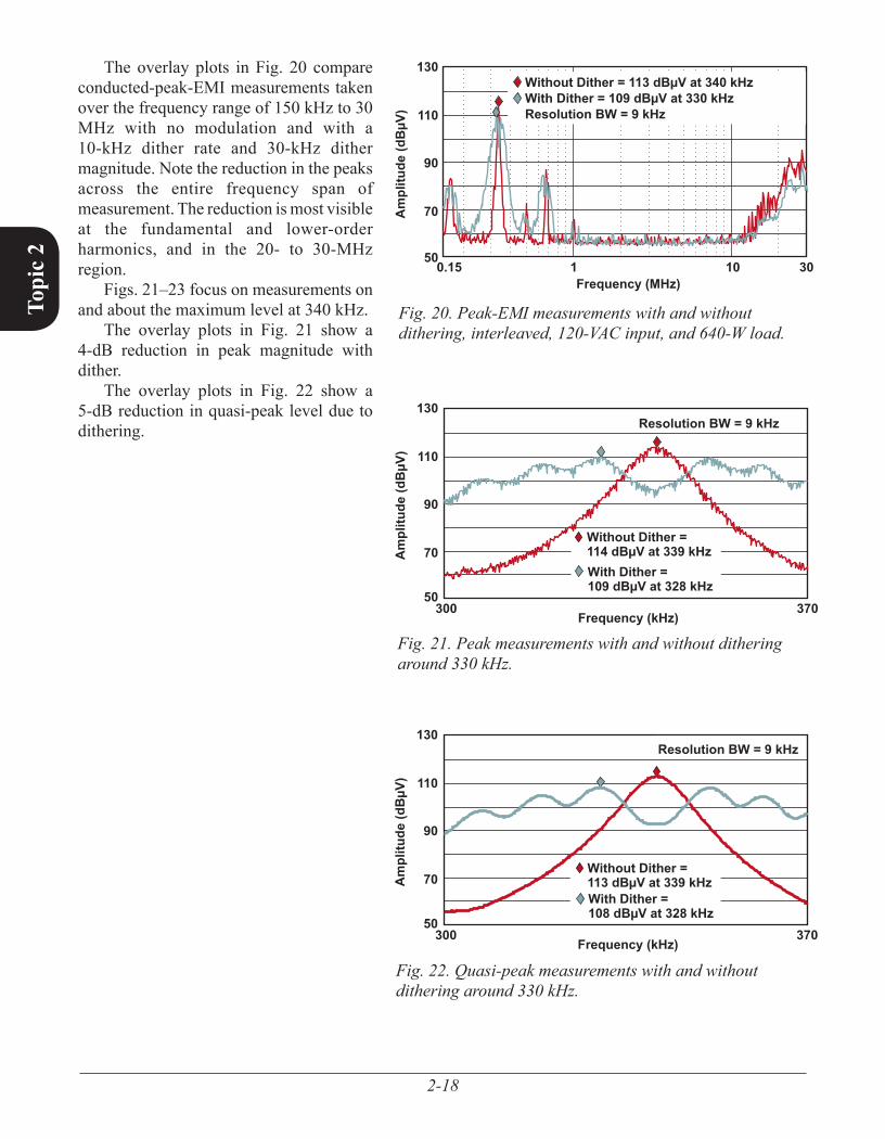
The overlay plots in Fig. 20 compare conducted-peak-EMI measurements taken over the frequency range of 150 kHz to 30 MHz with no modulation and with a 10-kHz dither rate and 30-kHz dither magnitude. Note the reduction in the peaks across the entire frequency span of measurement. The reduction is most visible at the fundamental and lower-order harmonics, and in the 20- to 30-MHz region.
Figs. 21–23 focus on measurements on and about the maximum level at 340 kHz.
The overlay plots in Fig. 21 show a 4-dB reduction in peak magnitude with dither.
The overlay plots in Fig. 22 show a 5-dB reduction in quasi-peak level due to dithering.
Frequency (MHz)
Amplitude(dBµV)
10.15 30
130
110
90
70
5010
Without Dither = 113 dBµV at 340 kHzWResolution BW = 9 kHzith Dither = 109 dBµV at 330 kHz
Fig. 20. Peak-EMI measurements with and without dithering, interleaved, 120-VAC input, and 640-W load.
Frequency (kHz)
Amplitu
de(dBµV
)
300
130
110
90
70
50370
Without Dither =114 dBµV at 339 kHzWith Dither =109 dBµV at 328 kHz
Resolution BW = 9 kHz
Fig. 21. Peak measurements with and without dithering around 330 kHz.
Fig. 22. Quasi-peak measurements with and without dithering around 330 kHz.
Frequency (kHz)
Amplitu
de(dBµV
)
300
130
110
90
70
50370
Without Dither =113 dBµV at 339 kHzWith Dither =108 dBµV at 328 kHz
Resolution BW = 9 kHz
2-19
Topi
c 2
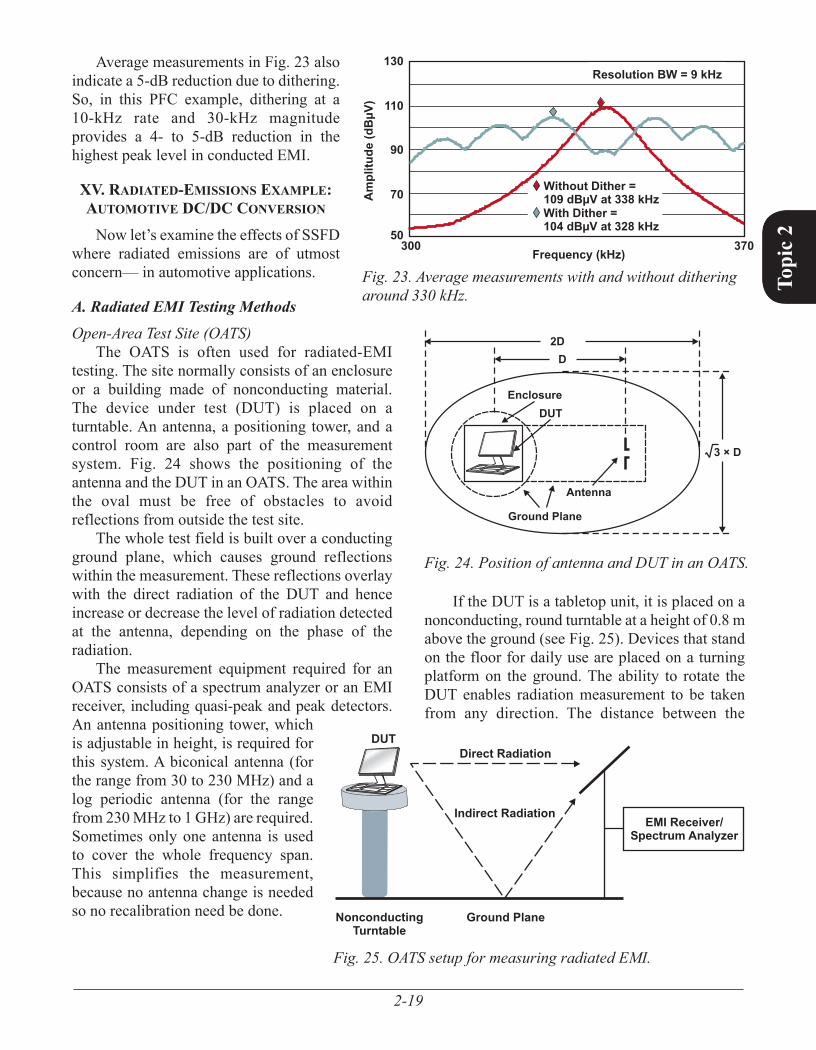
Average measurements in Fig. 23 also indicate a 5-dB reduction due to dithering. So, in this PFC example, dithering at a 10-kHz rate and 30-kHz magnitude provides a 4- to 5-dB reduction in the highest peak level in conducted EMI.
XV. rAdIAted-eMIssIons eXAMPle: AutoMotIVe dc/dc conVersIon
Now let’s examine the effects of SSFD where radiated emissions are of utmost concern— in automotive applications.
A. Radiated EMI Testing Methods
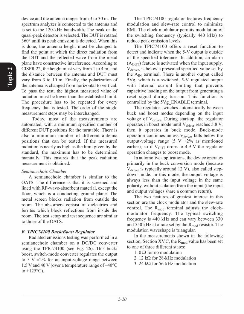
Open-Area Test Site (OATS)The OATS is often used for radiated-EMI
testing. The site normally consists of an enclosure or a building made of nonconducting material. The device under test (DUT) is placed on a turntable. An antenna, a positioning tower, and a control room are also part of the measurement system. Fig. 24 shows the positioning of the antenna and the DUT in an OATS. The area within the oval must be free of obstacles to avoid reflections from outside the test site.
The whole test field is built over a conducting ground plane, which causes ground reflections within the measurement. These reflections overlay with the direct radiation of the DUT and hence increase or decrease the level of radiation detected at the antenna, depending on the phase of the radiation.
The measurement equipment required for an OATS consists of a spectrum analyzer or an EMI re ceiver, including quasi-peak and peak detectors. An antenna position ing tower, which is adjustable in height, is required for this system. A biconical antenna (for the range from 30 to 230 MHz) and a log periodic antenna (for the range from 230 MHz to 1 GHz) are required. Sometimes only one antenna is used to cover the whole frequency span. This simplifies the measurement, because no antenna change is needed so no recalibration need be done.
Fig. 23. Average measurements with and without dithering around 330 kHz.
Frequency (kHz)
Amplitu
de(dBµV
)
300
130
110
90
70
50370
Without Dither =109 dBµV at 338 kHzWith Dither =104 dBµV at 328 kHz
Resolution BW = 9 kHz
Fig. 24. Position of antenna and DUT in an OATS.
Ground Plane
Antenna
Enclosure
2DD
DUT
3 × D
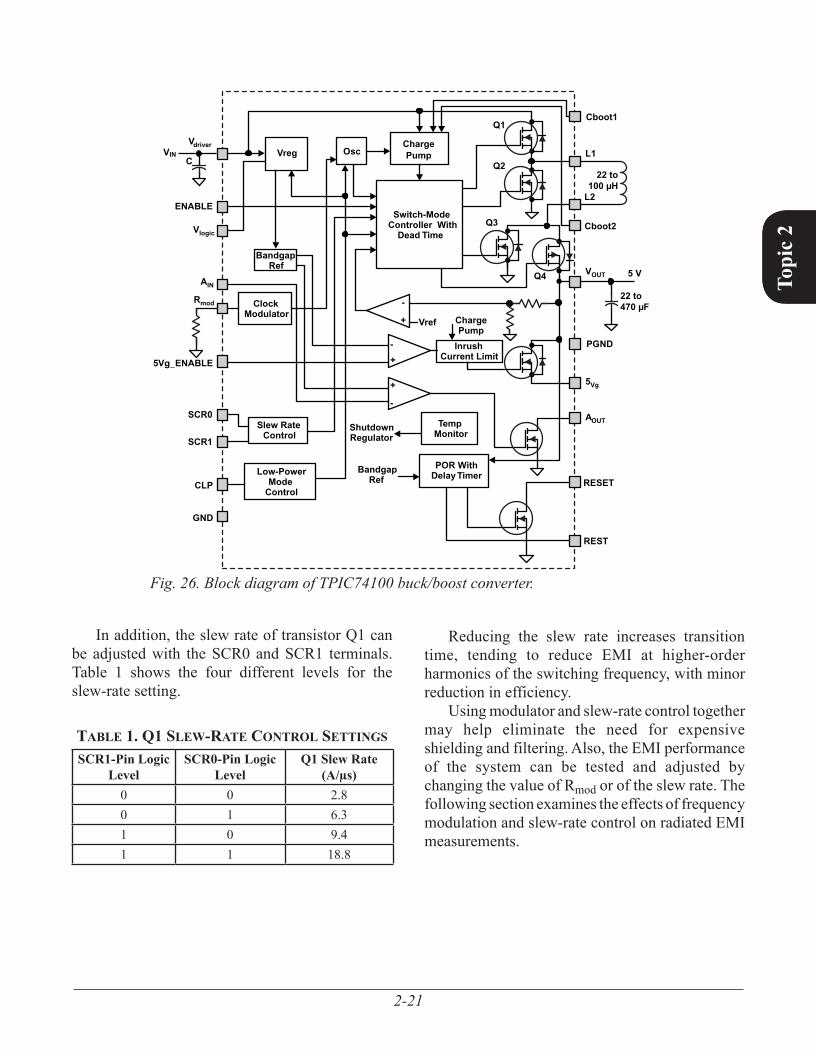
If the DUT is a tabletop unit, it is placed on a nonconducting, round turntable at a height of 0.8 m above the ground (see Fig. 25). Devices that stand on the floor for daily use are placed on a turning platform on the ground. The ability to rotate the DUT enables radiation measurement to be taken from any direction. The distance between the
Direct Radiation
Indirect RadiationEMI Receiver/
Spectrum Analyzer
Ground PlaneNonconductingTurntable
DUT
Fig. 25. OATS setup for measuring radiated EMI.
2-20
Topi
c 2
The TPIC74100 regulator features frequency modulation and slew-rate control to minimize EMI. The clock modulator permits modulation of the switching frequency (typically 440 kHz) to reduce peak emission levels.
The TPIC74100 offers a reset function to detect and indicate when the 5-V output is outside of the specified tolerance. In addition, an alarm (AOUT) feature is activated when the input supply, Vdriver, is below a prescaled specified value set by the AIN terminal. There is another output called 5Vg, which is a switched, 5-V regulated output with internal current limiting that prevents capacitive loading on the output from generating a reset signal during turn-on. This function is controlled by the 5Vg_ENABLE terminal.
The regulator switches automatically between buck and boost modes depending on the input voltage of Vdriver. During start-up, the regulator operates in boost mode until Vdriver reaches 5.8 V; then it operates in buck mode. Buck-mode operation continues unless Vdriver falls below the output-voltage range (5 V ±2% as mentioned earlier), so if VOUT drops to 4.9 V the regulator operation changes to boost mode.
In automotive applications, the device operates primarily in the buck conversion mode (because Vdriver is typically around 12 V), also called step-down mode. In this mode, the output voltage is always less than the input voltage in the same polarity, without isolation from the input (the input and output voltages share a common return).
The two features of greatest interest in this section are the clock modulator and the slew-rate control. The Rmod terminal adjusts the clock-modulator frequency. The typical switching frequency is 440 kHz and can vary between 330 and 550 kHz at a rate set by the Rmod resistor. The modulation waveshape is triangular.
In the measurements shown in the following section, Section XV.C, the Rmod value has been set to one of three different states:
1. 0 W for no modulation 2. 12 kW for 28-kHz modulation3. 24 kW for 56-kHz modulation
device and the antenna ranges from 3 to 30 m. The spectrum analyzer is connected to the antenna and is set to the 120-kHz bandwidth. The peak or the quasi-peak detector is selected. The DUT is rotated 360° until its peak emission is detected. When this is done, the antenna height must be changed to find the point at which the direct radiation from the DUT and the reflected wave from the metal plane have constructive interference. According to CISPR 22, the height must vary from 1 to 4 m, and the distance between the antenna and DUT must vary from 3 to 10 m. Finally, the polarization of the antenna is changed from horizontal to vertical. To pass the test, the highest measured value of radiation must be lower than the established limit. The procedure has to be repeated for every frequency that is tested. The order of the single measurement steps may be interchanged.
Today, most of the measurements are automated, with a minimum specified number of different DUT positions for the turntable. There is also a minimum number of different antenna positions that can be tested. If the measured radiation is nearly as high as the limit given by the standard, the maximum has to be determined manually. This ensures that the peak radiation measurement is obtained.
Semianechoic ChamberA semianechoic chamber is similar to the
OATS. The difference is that it is screened and lined with RF-wave-absorbent material, except the floor, which is a conducting ground plane. The metal screen blocks radiation from outside the room. The absorbers consist of dielectrics and ferrites which block reflections from inside the room. The test setup and test sequence are similar to those of the OATS.
B. TPIC74100 Buck/Boost RegulatorRadiated emissions testing was performed in a
semianechoic chamber on a DC/DC converter using the TPIC74100 (see Fig. 26). This buck/boost, switch-mode converter regulates the output to 5 V ±2% for an input-voltage range between 1.5 V and 40 V (over a temperature range of –40°C to +125°C).
2-21
Topi
c 2
In addition, the slew rate of transistor Q1 can be adjusted with the SCR0 and SCR1 terminals. Table 1 shows the four different levels for the slew-rate setting.
tAble 1. Q1 slew-rAte control settIngs
SCR1-Pin Logic Level
SCR0-Pin Logic Level
Q1 Slew Rate (A/µs)
0 0 2.8 0 1 6.31 0 9.41 1 18.8
Reducing the slew rate increases transition time, tending to reduce EMI at higher-order harmonics of the switching frequency, with minor reduction in efficiency.
Using modulator and slew-rate control together may help eliminate the need for expensive shielding and filtering. Also, the EMI performance of the system can be tested and adjusted by changing the value of Rmod or of the slew rate. The following section examines the effects of frequency modulation and slew-rate control on radiated EMI measurements.
Fig. 26. Block diagram of TPIC74100 buck/boost converter.
Switch-ModeController With
Dead Time
ChargePump
Vref
BandgapRef
Vreg Osc
+
-
+
-
POR WithDelay Timer
Vdriver
GND
L1
-
+
L2
VOUT
Q1
Q2
Q3
Q4
RESET
TempMonitor
ShutdownRegulator
Rmod ClockModulator
Cboot1
Cboot2
5Vg_ENABLE
AOUT
REST
PGND
SCR0
SCR1
Slew RateControl
5Vg
Low-PowerMode
ControlCLP
InrushCurrent Limit
ChargePump
BandgapRef
Vlogic
AIN
ENABLE
C22 to
100 µH
5 V
22 to470 µF
VIN
2-22
Topi
c 2 +
VO
UT
VOUT+
Vlogic
1
2
3
4
5
6
7
8
9
10
SCR1
Cboot2
Cboot1
Vdriver
L1
PGND
L2
VOUT
5Vg
AIN
U1TPIC74100
TP3PGND
TP4VOUT
TP1Ign
TP2PGND
D1
ES3D
JP1
L2 B
ypas
sC1
SPARE
Vlogic
R1SPARE
C24.7 nF
C34.7 nF
L133 µH
C5470 µF
C6100 nF
SCR0
5Vg_ENABLE
ENABLE
Vlogic
GND
Rmod
REST
AOUT
RESET
CLP
20
19
18
17
16
15
14
13
12
11
GND/PWP
C8100 nF
C947 µF
C1110 nF
R768 kΩ
R1033 kΩ
L233 µH
C123.3 nF
C1010 nF
C4470 nF
C7100 nF
R820 kΩ
R612 kΩ
R920 kΩ
C. TPIC74100 Radiated-Emissions TestingFor the measurements, an off-the-shelf
TPIC74100 EVM2 was used (see Fig. 27), which was not optimized for EMC. Two modifications were applied before measurements were taken:
Two 2-µF, 50-V X7R capacitors were placed in • parallel with input capacitor C5 (470-µF electrolytic).L2 input inductor was bypassed by • connecting jumper JP1.
The TPIC74100 in this buck configuration drives 625-mA current into an 8-W load from a 5-V output. For the test setup, the CISPR 25 Class 5 requirements were used, with 1-m monopole and biconical antennas. The EVM2 board was powered via a 1.7-m-long, unshielded twisted pair from a car battery and an LISN. Either no modulation or a modulation frequency of 28 or 56 kHz was chosen for the test, in combination with the four different settings of the slew rate, in order to compare the impact of the settings.
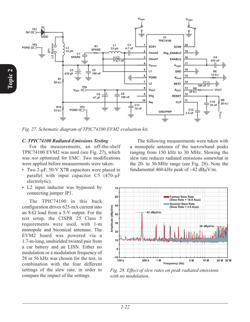
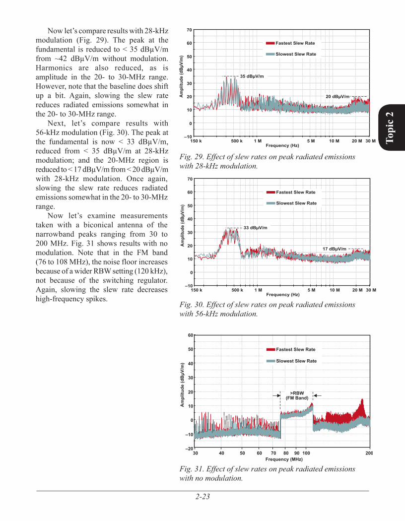
The following measurements were taken with a monopole antenna of the narrowband peaks ranging from 150 kHz to 30 MHz. Slowing the slew rate reduces radiated emissions somewhat in the 20- to 30-MHz range (see Fig. 28). Note the fundamental 460-kHz peak of ~42 dBµV/m.
Fig. 27. Schematic diagram of TPIC74100 EVM2 evaluation kit.
–10
0
10
20
30
40
50
60
70
150 k 500 k 1 M 5 M 10 M 20 M 30 M
Amplitu
de(dBµV
/m)
Frequency (Hz)
Fastest Slew Rate(Slew Rate = 18.8 A/µs)Slowest Slew Rate(Slew Rate = 2.8 A/µs)
42 dBµV/m
26 dBµV/m
Fig. 28. Effect of slew rates on peak radiated emissions with no modulation.
2-23
Topi
c 2
Now let’s compare results with 28-kHz modulation (Fig. 29). The peak at the fundamental is reduced to < 35 dBµV/m from ~42 dBµV/m without modulation. Harmonics are also reduced, as is amplitude in the 20- to 30-MHz range. However, note that the baseline does shift up a bit. Again, slowing the slew rate reduces radiated emissions somewhat in the 20- to 30-MHz range.
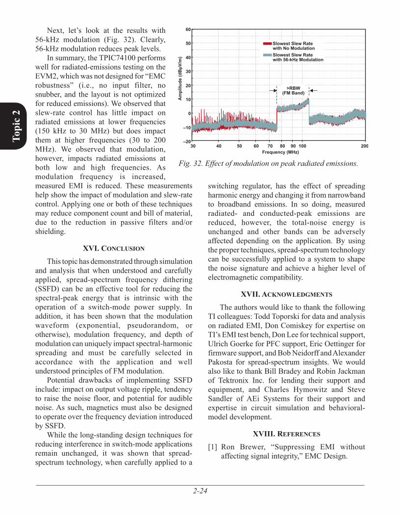
Next, let’s compare results with 56-kHz modulation (Fig. 30). The peak at the fundamental is now < 33 dBµV/m, reduced from < 35 dBµV/m at 28-kHz modulation; and the 20-MHz region is reduced to < 17 dBµV/m from < 20 dBµV/m with 28-kHz modulation. Once again, slowing the slew rate reduces radiated emissions somewhat in the 20- to 30-MHz range.
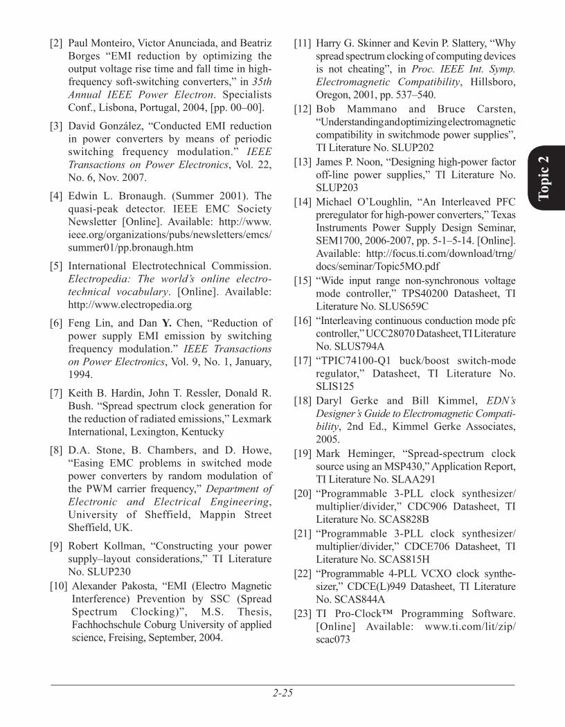
Now let’s examine measurements taken with a biconical antenna of the narrowband peaks ranging from 30 to 200 MHz. Fig. 31 shows results with no modulation. Note that in the FM band (76 to 108 MHz), the noise floor increases because of a wider RBW setting (120 kHz), not because of the switching regulator. Again, slowing the slew rate decreases high-frequency spikes.
–10
0
10
20
30
40
50
60
70
150 k 500 k 1 M 5 M 10 M 20 M 30 M
Amplitu
de(dBµ
V/m)
Frequency (Hz)
Fastest Slew Rate
Slowest Slew Rate
35 dBµV/m
20 dBµV/m
–10
0
10
20
30
40
50
60
70
150 k 500 k 1 M 5 M 10 M 20 M 30 M
Amplitu
de(dBµ
V/m)
Frequency (Hz)
Fastest Slew Rate
Slowest Slew Rate
33 dBµV/m
17 dBµV/m
–20
–10
0
10
20
30
40
50
60
30 40 50 60 70 80 90 100 200
Amplitu
de(dBµV
/m)
Frequency (MHz)
Fastest Slew Rate
>RBW(FM Band)
Slowest Slew Rate
Fig. 29. Effect of slew rates on peak radiated emissions with 28-kHz modulation.
Fig. 30. Effect of slew rates on peak radiated emissions with 56-kHz modulation.
Fig. 31. Effect of slew rates on peak radiated emissions with no modulation.
2-24
Topi
c 2
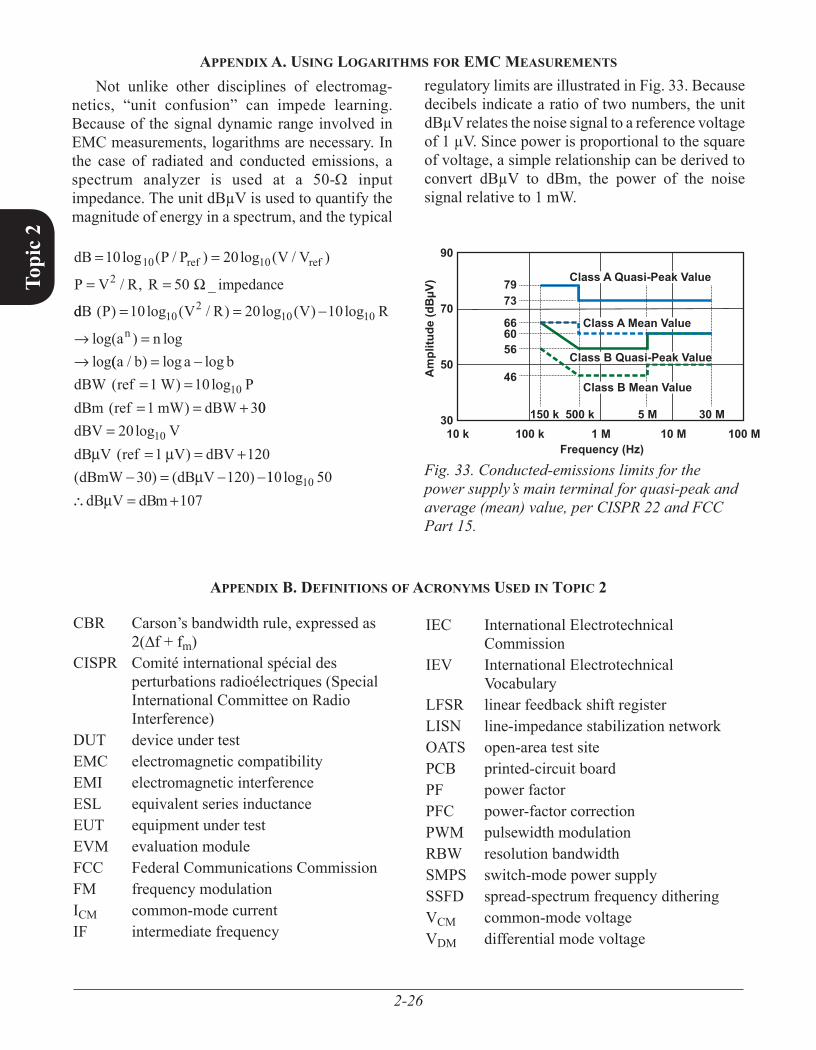
Next, let’s look at the results with 56-kHz modulation (Fig. 32). Clearly, 56-kHz modulation reduces peak levels.
In summary, the TPIC74100 performs well for radiated-emissions testing on the EVM2, which was not designed for “EMC robustness” (i.e., no input filter, no snubber, and the layout is not optimized for reduced emissions). We observed that slew-rate control has little impact on radiated emissions at lower frequencies (150 kHz to 30 MHz) but does impact them at higher frequencies (30 to 200 MHz). We observed that modulation, however, impacts radiated emissions at both low and high frequencies. As modulation frequency is increased, measured EMI is reduced. These measurements help show the impact of modulation and slew-rate control. Applying one or both of these techniques may reduce component count and bill of material, due to the reduction in passive filters and/or shielding.
XVI. conclusIon
This topic has demonstrated through simulation and analysis that when understood and carefully applied, spread-spectrum frequency dithering (SSFD) can be an effective tool for reducing the spectral-peak energy that is intrinsic with the operation of a switch-mode power supply. In addition, it has been shown that the modulation waveform (exponential, pseudorandom, or otherwise), modulation frequency, and depth of modulation can uniquely impact spectral-harmonic spreading and must be carefully selected in accordance with the application and well understood principles of FM modulation.
Potential drawbacks of implementing SSFD include: impact on output voltage ripple, tendency to raise the noise floor, and potential for audible noise. As such, magnetics must also be designed to operate over the frequency deviation introduced by SSFD.
While the long-standing design techniques for reducing interference in switch-mode applications remain unchanged, it was shown that spread- spectrum technology, when carefully applied to a
–20
–10
0
10
20
30
40
50
60
30 40 50 60 70 80 90 100 200
Amplitu
de(dBµV
/m)
Frequency (MHz)
Fastest Slew Rate
Slowest Slew Rate
Slowest Slew Ratewith No ModulationSlowest Slew Ratewith 56-kHz Modulation
>RBW(FM Band)
Fig. 32. Effect of modulation on peak radiated emissions.
switching regulator, has the effect of spreading harmonic energy and changing it from narrowband to broadband emissions. In so doing, measured radiated- and conducted-peak emissions are reduced, however, the total-noise energy is unchanged and other bands can be adversely affected depending on the application. By using the proper techniques, spread-spectrum tech nology can be successfully applied to a system to shape the noise signature and achieve a higher level of electromagnetic compatibility.
XVII. AcknowledgMents
The authors would like to thank the following TI colleagues: Todd Toporski for data and analysis on radiated EMI, Don Comiskey for expertise on TI’s EMI test bench, Don Lee for technical support, Ulrich Goerke for PFC support, Eric Oettinger for firmware support, and Bob Neidorff and Alexander Pakosta for spread-spectrum insights. We would also like to thank Bill Bradey and Robin Jackman of Tektronix Inc. for lending their support and equipment, and Charles Hymowitz and Steve Sandler of AEi Systems for their support and expertise in circuit simulation and behavioral-model development.
XVIII. references
[1] Ron Brewer, “Suppressing EMI without affecting signal integrity,” EMC Design.
2-25
Topi
c 2
[2] Paul Monteiro, Victor Anunciada, and Beatriz Borges “EMI reduction by optimizing the output voltage rise time and fall time in high-frequency soft-switching converters,” in 35th Annual IEEE Power Electron. Specialists Conf., Lisbona, Portugal, 2004, [pp. 00–00].
[3] David González, “Conducted EMI reduction in power converters by means of periodic switching frequency modulation.” IEEE Transactions on Power Electronics, Vol. 22, No. 6, Nov. 2007.
[4] Edwin L. Bronaugh. (Summer 2001). The quasi-peak detector. IEEE EMC Society Newsletter [Online]. Available: http://www.ieee.org/organizations/pubs/newsletters/emcs/summer01/pp.bronaugh.htm
[5] International Electrotechnical Commission. Electropedia: The world’s online electro-technical vocabulary. [Online]. Available: http://www.electropedia.org
[6] Feng Lin, and Dan Y. Chen, “Reduction of power supply EMI emission by switching frequency modulation.” IEEE Transactions on Power Electronics, Vol. 9, No. 1, January, 1994.
[7] Keith B. Hardin, John T. Ressler, Donald R. Bush. “Spread spectrum clock generation for the reduction of radiated emissions,” Lexmark International, Lexington, Kentucky
[8] D.A. Stone, B. Chambers, and D. Howe, “Easing EMC problems in switched mode power converters by random modulation of the PWM carrier frequency,” Department of Elect ronic and Electrical Engineering, University of Sheffield, Mappin Street Sheffield, UK.
[9] Robert Kollman, “Constructing your power supply–layout considerations,” TI Literature No. SLUP230
[10] Alexander Pakosta, “EMI (Electro Magnetic Interference) Prevention by SSC (Spread Spectrum Clocking)”, M.S. Thesis, Fachhochschule Coburg University of applied science, Freising, September, 2004.
[11] Harry G. Skinner and Kevin P. Slattery, “Why spread spectrum clocking of computing devices is not cheating”, in Proc. IEEE Int. Symp. Electromagnetic Compatibility, Hillsboro, Oregon, 2001, pp. 537–540.
[12] Bob Mammano and Bruce Carsten, “Understanding and optimizing electromagnetic compatibility in switchmode power supplies”, TI Literature No. SLUP202
[13] James P. Noon, “Designing high-power factor off-line power supplies,” TI Literature No. SLUP203
[14] Michael O’Loughlin, “An Interleaved PFC preregulator for high-power converters,” Texas Instruments Power Supply Design Seminar, SEM1700, 2006-2007, pp. 5-1–5-14. [Online]. Available: http://focus.ti.com/download/trng/docs/seminar/Topic5MO.pdf
[15] “Wide input range non-synchronous voltage mode controller,” TPS40200 Datasheet, TI Literature No. SLUS659C
[16] “Interleaving continuous conduction mode pfc controller,” UCC28070 Datasheet, TI Literature No. SLUS794A
[17] “TPIC74100-Q1 buck/boost switch-mode regulator,” Datasheet, TI Literature No. SLIS125
[18] Daryl Gerke and Bill Kimmel, EDN’s Designer’s Guide to Electromagnetic Compati-bility, 2nd Ed., Kimmel Gerke Associates, 2005.
[19] Mark Heminger, “Spread-spectrum clock source using an MSP430,” Application Report, TI Literature No. SLAA291
[20] “Programmable 3-PLL clock synthesizer/multiplier/divider,” CDC906 Datasheet, TI Literature No. SCAS828B
[21] “Programmable 3-PLL clock synthesizer/multiplier/divider,” CDCE706 Datasheet, TI Literature No. SCAS815H
[22] “Programmable 4-PLL VCXO clock synthe-sizer,” CDCE(L)949 Datasheet, TI Literature No. SCAS844A
[23] TI Pro-Clock™ Programming Software. [Online] Available: www.ti.com/lit/zip/scac073
2-26
Topi
c 2
APPendIX A. usIng logArIthMs for eMc MeAsureMents
Not unlike other disciplines of electromag-netics, “unit confusion” can impede learning. Because of the signal dynamic range involved in EMC measurements, logarithms are necessary. In the case of radiated and conducted emissions, a spectrum analyzer is used at a 50-W input impedance. The unit dBµV is used to quantify the magnitude of energy in a spectrum, and the typical
CBR Carson’s bandwidth rule, expressed as 2(∆f + fm)
CISPR Comité international spécial des perturbations radioélectriques (Special International Committee on Radio Interference)
DUT device under testEMC electromagnetic compatibilityEMI electromagnetic interferenceESL equivalent series inductanceEUT equipment under testEVM evaluation moduleFCC Federal Communications CommissionFM frequency modulationICM common-mode currentIF intermediate frequency
Fig. 33. Conducted-emissions limits for the power supply’s main terminal for quasi-peak and average (mean) value, per CISPR 22 and FCC Part 15.
Frequency (Hz)10 k 100 k
150 k 500 k 5 M
7973
666056
46
30 M1 M 10 M 100 M
90
70
50
30Amplitu
de(dBµV
) Class A Quasi-Peak Value
Class B Quasi-Peak Value
Class A Mean Value
Class B Mean Value
APPendIX b. defInItIons of AcronyMs used In toPIc 2
IEC International Electrotechnical Commission
IEV International Electrotechnical Vocabulary
LFSR linear feedback shift registerLISN line-impedance stabilization networkOATS open-area test sitePCB printed-circuit boardPF power factorPFC power-factor correctionPWM pulsewidth modulationRBW resolution bandwidthSMPS switch-mode power supplySSFD spread-spectrum frequency ditheringVCM common-mode voltageVDM differential mode voltage
regulatory limits are illustrated in Fig. 33. Because decibels indicate a ratio of two numbers, the unit dBµV relates the noise signal to a reference voltage of 1 µV. Since power is proportional to the square of voltage, a simple relationship can be derived to convert dBµV to dBm, the power of the noise signal relative to 1 mW.
dB P P V V
P V R R impedanceref ref= =
= =
10 20
5010 10
2
log ( / ) log ( / )
/ , _ Ω
ddB P V R V R
a nn
( ) log ( / ) log ( ) log
log( ) loglog
= = −
→ =→
10 20 10102
10 10
(( / ) log log( ) log( )
a b a bdBW ref W PdBm ref mW dBW
= −= == = +
1 101 3
10
0020
1 12030 120
10dBV VB V ref V dBVdBmW dB V
== = +
− = − −
log( )
( ) ( )d µ µ
µ 110 50107
10log∴ = +dB V dBmµ