Embed Size (px)
Citation preview

VOLTAGE CONTROL OF DC-DC BUCK CONVERTER AND ITS
REAL TIME IMPLEMENTATION USING
MICROCONTROLLER
Submitted by
DIPAK KUMAR DASH
Roll No-211EE2380
M. Tech. in Power Control & Drives
Dept. of Electrical Engineering
Under the Guidance of
Prof. Bidyadhar Subudhi
DEPARTMENT OF ELECTRICAL ENGINEERING
NATIONAL INSTITUTE OF TECHNOLOGY
ROURKELA-769008

Dipak kumar Dash

VOLTAGE CONTROL OF DC-DC BUCK CONVERTER AND ITS REAL
TIME IMPLEMENTATION USING MICROCONTROLLER
Thesis submitted in partial fulfilment of the requirements for the award of the Master of Technology in Electrical Engineering with Specialization in
“Power Control and Drives”
By
Dipak kumar Dash
Roll No: 211EE2380
May-2013
Under the guidance of
Dr. Bidyadhar Subudhi
Dept. of Electrical Engineering
National Institute of Technology
Rourkela-769008

Dedicated to my family & teachers

i
This is to certify that the Thesis Report entitled “Voltage Control of DC-DC Buck Converter and
its Real Time Implementation Using a Microcontroller, submitted by Mr Dipak Kumar Dash
bearing roll no. 211EE2380 in partial fulfilment of the requirements for the award of Master of
Technology in Electrical Engineering with specialization in “Power Control and Drives” during
session 2011-2013 at National Institute of Technology, Rourkela is an authentic work carried out
by him under my supervision and guidance. I believe that the thesis fulfils part of the requirements
for the award of degree of Master of Technology in Power Control and Drives. The results
embodied in the thesis have not been submitted for award of any other degree.
Dr.Bidyadhar Subudhi
Dept. of Electrical Engineering
National Institute of Technology
Rourkela-769008
CERTIFICATE
Department of Electrical Engineering
National Institute of Technology, Rourkela
Odisha, INDIA - 769008

ii
DECLARATION
I hereby declare that the investigation carried out in the thesis has been carried out by me. The
work is original and has not been submitted earlier as a whole or in part for a degree/diploma at
this or any other institution / University.
Dipak Kumar Dash

iii
ACKNOWLEDGEMENTS
I wish to express my sincere thanks and deep sense of gratitude to Dr.Bidyadhar
Subudhi, for his inspiration, tremendous support, vision, and dedication to the successful
completion of this work. His futuristic vision and realistic ideas have created an ever increasing
zeal to work and explore many new things. He has been a great source of inspiration to work
with and I shall always cherish my association with him with immense pleasure.
I thank Prof. Anup Kumar Panda, Head of the Department of Electrical Engineering,
National Institute of Technology, Rourkela, for providing me facilities to carry out my thesis
work in the Department of Electrical Engineering.
My sincere gratitude to all the faculty members of Department of Electrical Engineering,
NIT Rourkela for their affection and support.
I will be failing in my duty if I do not express my thanks to the staff of Electrical
Engineering Department for their timely help as and when require.
Words fail to express my deep sense of gratitude especially towards my family members
for their patient love, moral encouragement and support which enabled me to complete this
course. I thank all my friends who have extended their cooperation and suggestions by way of
discussion at various steps in completion of this thesis. Finally, I would like to thank the
almighty to enlighten the ignorance with in me and supporting me in my ups and downs to
always fight back.
Dipak Kumar Dash

iv
ABSTRACT
The switched mode dc-dc converters are some of the simplest power electronic circuits
which convert one level of electrical voltage into another level by switching action. These
converters have received an increasing deal of interest in many areas. This is due to their wide
applications like power supplies for personal computers, office equipment, appliance control,
telecommunication equipment, DC motor drives, automotive, aircraft, etc. The analysis, control
and stabilization of switching converters are the main factors that need to be considered. Many
control methods are used for control of switch mode dc-dc converters and the simple and low
cost controller structure is always in demand for most industrial and high performance
applications. Every control method has some advantages and drawbacks due to which that
particular control method consider as a suitable control method under specific conditions,
compared to other control methods. The voltage control of buck converter using PI, PID
controller ,PIDSMC and microcontroller based PID control are modeled and are evaluated by
computer simulations.. In addition to this, the closed loop feedback system using PID
controller method will be implemented against transient response in the system. This project is
only limited to design the closed-loop feedback system using proportional technique for buck
converter. The controller will be implemented on a PIC microcontroller (PIC16F4011) and
programmed through a computer using software of Mp Lab C compiler. The programmed
PIC16F4011 will be able to automatically control the duty cycle of the system in order to apply
an appropriate duty cycle to the system. It has been found that the transient performance and
steady state performance is improved using microcontroller based PID controller. The
simulated open loop and closed loop performance is verified experimentally. The experimental
system is found to be more advantageous and cost effective with microcontroller.

v
TABLE OF CONTENTS
CHAPTER TITLE PAGE
CERTIFICATE i
DECLARATION ii
ACKNOLEDGEMENTS iii
ABSTRACT iv
TABLE OF CONTENTS v
LIST OF FIGURES vii
LIST OF TABLES ix
1 INTRODUCTION 1
1.1. Overview
1.2. Motivation
1.3. Objective of research
1.4. Research background
1.5. Thesis organisation
1
2
2
3
5
2
DISCUSSION AND ANALYSIS OF VARIOUS
CONVERTER TOPOLOGIES
6
2.1. Introduction
2.2. Dc-Dc Buck converter
2.3. Buck converter in open loop mode
2.3.1. Parameters
2.3.2. Results obtained from Simulink model of buck
converter
2.4. Summary
6
7
8
9
10
12

vi
3
ANALYSIS OF BUCK CONVERTER OUTPUT WITH
DIFFERENT CONTROLLER
13
3.1. Introduction
3.2. PI Controller
3.3. PID Controller
3.4. Sliding mode PID Controller
3.5. Summary
13
13
14
21
18
28
4
REALTIME IMPLIMENTATION OF BUCK CONVERTER
USING MICROCONTROLLER WITH PID LOGIC 29
4.1. Design concept
4.2. Components Review
4.3. Microcontroller implemented with PID
4.4. PIC Microcontroller Tools Development
4.5. Methodology
4.6. Results and Discussion
4.7. Summary
30
30
33
35
36
41
41
5 CONCLUSION AND FUTURE WORK 42

vii
LIST OF FIGURES
Fig. 2.1 DC-DC Buck converter 7
Fig. 2.2 Operating modes of buck converter 7
Fig. 2.3 Simulunk model of buck converter in open loop 10
Fig. 2.4 Capacitor voltage in open loop 11
Fig. 2.5 Inductor current in open loop 11
Fig. 2.6 Output voltage in open loop 11
Fig. 3.1 Control circuit for DC-DC converter 13
Fig. 3.2.1 Simulink model of buck converter with PID controller 14
Fig. 3.2.2
Output voltage response obtained from MATLAB/SIMULINK with PI
controller.
20
Fig. 3.2.3
Inductor current response obtained from MATLAB/SIMULINK with
PI controller.
21
Fig. 3.3.1 MATLAB Simulink model with PID Controller 24
Fig. 3.3.2 Buck converter responses with PID controller 25
Fig. 3.3.3 Output current with PID controller 26
Fig.3.4
Derived model of Sliding mode PID controller for voltage control
of buck converter
27
Fig. 4.1 Pin configuration of TLP250 31
Fig. 4.2 Pin configuration of IRF 540 32
Fig. 4.3 Pin configuration of PIC30F4011 33
Fig. 4.4 Mp lab screen shots 36

viii
Fig. 4.5 Design of buck converter with PID implemented microcontroller 37
Fig. 4.6 Buck converter circuit 38
Fig. 4.7 Model of buck converter with microcontroller 39
Fig. 4.8
Responses of buck converter obtained from microcontroller
implemented PID control
40

ix
LIST OF TABLES
Table 2.1 Parameters of MATLAB/Simulink model for Buck converter [7]. 9
Table 3.1 Gains in PID control equivalent model[23] 25
Table 3.1 SMCPID buck converter prototype design parameters [23] 26
Table 3.3 Results obtained in implementation of different controllers 28
1
1.1. Overview
Switch mode DC-DC converters efficiently convert an unregulated DC input voltage
into a regulated DC output voltage. Compared to linear power supplies, switching power
supplies provide much more efficiency and power density. Switching power supplies employ
solid-state devices such as transistors and diodes to operate as a switch: either completely on
or completely off. Energy storage elements, including capacitors and inductors, are used for
energy transfer and work as a low-pass filter. The buck converter and the boost converter are
the two fundamental topologies of switch mode DC-DC converters. Most of the other
topologies are either buck-derived or boost-derived converters, because their topologies are
equivalent to the buck or the boost converters. Traditionally, the control methodology for
DC-DC converters has been analog control. In the recent years, technology advances in very-
large-scale integration (VLSI) have made digital control of DC-DC converters with
microcontrollers and digital signal processors (DSP) possible. The major advantages of
digital control over analog control are higher immunity to environmental changes such as
temperature and aging of components, increased flexibility by changing the software, more
advanced control techniques and shorter design cycles. Generally, DSPs have more
computational power than microcontrollers. Therefore, more advanced control algorithms can
be implemented on a microcontroller.
Switch-mode DC-DC converters are used to convert the unregulated DC input to a
controlled DC output at a desired voltage level. Switch-mode DC-DC converters include
buck converters, boost converters, buck-boost converters, Cuk converters and full-bridge
converters, etc. Among these converters, the buck converter and the boost converter are the
basic topologies. Both the buck-boost and Cuk converters are combinations of the two basic
topologies. The full-bridge converter is derived from the buck converter.
There are usually two modes of operation for DC-DC converters: continuous and
discontinuous. The current flowing through the inductor never falls to zero in the continuous
mode. In the discontinuous mode, the inductor current falls to zero during the time the switch
is turned off. Only operation in the continuous mode is considered in this dissertation.

2
1.2. Motivation
The switched mode dc-dc converters are some of the simplest power electronic
circuits which convert one level of electrical voltage into another level by switching action.
These converters have received an increasing deal of interest in many areas. This is due to
their wide applications like power supplies for personal computers, office equipment,
appliance control, telecommunication equipment, DC motor drives, automotive, aircraft, etc.
The analysis, control and stabilization of switching converters are the main factors that need
to be considered. Many control methods are used for control of switch mode dc-dc converters
and the simple and low cost controller structure is always in demand for most industrial and
high performance applications. Every control method has some advantages and drawbacks
due to which that particular control method consider as a suitable control method under
specific conditions, compared to other control methods. The control method that gives the
best performances under any conditions is always in demand.
1.3 Thesis objectives
To design a DC-DC buck converter of 24V/3V.
To design a PID controller to obtain constant output voltage.
Implementation of PID controller logic in microcontroller.
To design SMC and implementation in microcontroller.
1.4 Literature Review
Voltage-mode control and Current-mode control are two commonly used control
schemes to regulate the output voltage of dc-dc converters. Both control schemes have been
widely used in low-voltage low-power switch-mode dc-dc converters integrated circuit
design in industry. Feedback loop method automatically maintains a precise output voltage
regardless of variation in input voltage and load conditions. Currently, there exist many
different approaches that have been proposed for the PWM switching control design, e.g.,
state space averaging methods PID control, optimal control, sliding mode control and fuzzy
control etc.
The dc-dc switching converters are the widely used circuits in electronics systems. They are
usually used to obtain a stabilized output voltage from a given input DC voltage which is
lower (buck) from that input voltage, or higher (boost) or generic (buck–boost). Each of these

3
circuits is basically composed of transistor and diode making up the switching circuit and
inductor and capacitor building the filter circuit. In addition to these, the circuit may have
feedback circuit for the purpose of controlling the output parameters [1]. The design of buck
converters and boost converters with a review over their state space equations led us to the
derivative that the operation of such dc-dc converters is performed through two modes let the
first mode be the on-state and the later is the off-state depending on the switching circuit [2-
4]. After the study of the state space model of the converters the basic controlling circuits
were implemented through voltage control, current control, PI and PID control techniques
which were best for steady state analysis. However their performance was questioned for
transient analysis [3-5]. This motivated the development of several non-linear control
techniques for dc-dc converters like sliding mode control, hysteresis control etc. [6-7]. But
the difficulty in implementing their mathematical model to the physical circuit led to the
development of various feedback controllers [10].Switched mode dc-dc converters represent
a particular class of the VSS, since there structure is periodically changed by the action of
controlled switches and diodes. So it is appropriate to use sliding mode controllers in dc-dc
converters [11].The use of SM (nonlinear) controllers can maintain a good regulation for a
wide operating range. So, a lot of interest is developed in the use of SM controllers for dc-dc
converters [12]. Siew-Chong Tan presented a detail discussion on the use of SM control for
dc-dc power converters [13].Then SM controller is applied in higher order converters in 1989
[14]. Huang et al. applied SM control for cuk switching regulator. After this, series of related
works on the cuk converter was carried out [15]-[18]. Fossas and Pas [19] applied a second-
order SM control algorithms to buck converter for reduction of chattering. Then, two types of
SM-control for boost and buck-boost converters: one using the method of stable system
centre [20] and the other using sliding dynamic manifold [21] is proposed by Yuri
B.Mattavelli et al. [22] proposed a general-purpose sliding-mode controller, which is
applicable to most dc-dc converter topologies. The circuit complexity is same as current-
mode controllers and it provides extreme robustness and speed of response against line, load
and parameter variations. The same group derived small signal models for dc-dc converters
with SM control, which allows the selection of control coefficients, the analysis of parameter
variation effects, the evaluation of the closed loop performances like audio susceptibility,
output and input impedances, and reference to output transfer function [23].Zhang li and
QIU Shui-sheng implemented Proportional-Integral sliding mode controller in dc-dc
converters. They showed that the implementation of PI SM control is simpler than other SM
control schemes and steady state error is eliminated [24].Mahadeviet al. [25] Proposed state

4
space averaging method to PWM based SM controlled dc-dc converters with a constant
switching frequency. They also applied neural networks into their PWM-based SM controlled
converters [26].Dc-dc converters can be operated either in continuous conduction mode
(CCM) or in discontinuous conduction mode (DCM). Dc-dc converters that operated in DCM
provide faster transient response (due to its low inductance) at the expense of higher device
stresses. He also presented a fixed frequency PWM based sliding mode controllers for dc-dc
converters operating in DCM [27]-[28].
1.5 Thesis Organisation
This thesis consists of this introductory chapter and five other chapters arranged as
follows:
Chapter.1 covers the basic ideas, introduction, literature survey and the objective of the
thesis.
Chapter.2. describes different converter topologies and their different mode of operation in
MATLAB/SIMULINK environment.
Chapter .3 concerns about the different types of controllers that can be applied to dc-dc buck
converter in MATLAB/ SIMULINK and analysis of results obtained in various cases using
different controller topology for output voltage of dc-dc buck converter.
Chapter.4 covers the design procedure of dc-dc buck converter using microcontroller with
PID algorithm as the base.
Chapter. 5 cover general conclusions and future scope with references and appendices.

5
DISCUSSION AND ANALYSIS OF VARIOUS CONVERTER TOPOLOGIES
2.1 Background
The switching converters convert one level of electrical voltage into another level by
switching action. They are popular because of their smaller size and efficiency compared to
the linear regulators. DC-DC converters have a very large application area. These are used
extensively in personal computers, computer peripherals, and adapters of consumer electronic
devices to provide dc voltages.
There are some different methods of classifying dc-dc converters. One of them
depends on the isolation property of the primary and secondary portion. The isolation is
usually made by a transformer, which has a primary portion at input side and a secondary at
output side. Feedback of the control loop is made by another smaller transformer. Therefore,
output is electrically isolated from the input. This type includes Fly-back dc-dc converters.
However, in portable devices, since the area to implement this bulky transformer and other
off-chip components is very big and costly, so non-isolation dc-dc converters are more
preferred. The non-isolated dc/dc converters can be classified as follows:
• Buck converter (step down dc-dc converter),
• Boost converter (step up dc-dc converter),
• Buck-Boost converter (step up-down dc-dc converter, opposite polarity), and
• Cuk converter (step up-down dc-dc converter).
The dc-dc buck converters and the dc-dc boost converter are the simplest power
converter circuits used for many power management and voltage regulator applications.

6
Hence, the analysis and design of the control structure is done for these basic converter
circuits.
2.2 DC-DC BUCK CONVERTER
The buck converter circuit converts a higher dc input voltage to lower dc output
voltage. The basic buck dc-dc converter topology is shown
Fig.2.1 DC-DC buck converter
Fig. 2.2 Operating Modes of Buck Converter
a: On State b: Off State
It consists of a controlled switch (SW), an uncontrolled switch (D), an inductor (L), a
capacitor(C), and a load resistance(R).

7
The first sub-circuit state is when the switch is turned on, diode is reverse biased and
inductor current flows through the switch. When the switch (SW) is on and D is reverse
biased, the dynamics of inductor current (IL) and the capacitor voltage (VC) are
d (t)
( ) (2.1)
( ) (2.2)
The second sub-circuit state is when the switch is turned off and current freewheels
through the diode. When the switch Swiss off and D is forward biased, the dynamics of the
circuit are
d (t)
(2.3)
( ) (2.4)
The operation of dc-dc converters can be classified by the continuity of inductor
current flow. So dc-dc converter has two different modes of operation that are
(a) Continuous conduction mode (CCM)
(b) Discontinuous conduction mode (DCM)
A converter can be designed in any mode of operation according to the desired value.
When the inductor current flow is continuous of charge and discharge during a switching
period, it is called Continuous Conduction Mode (CCM).When the inductor current has an
interval of time staying at zero with no charge and discharge then it is said to be working in
Discontinuous Conduction Mode (DCM) operation and the waveform of inductor current.
2.3 BUCK CONVERTER IN OPEN LOOP MODE
To demonstrate the performance of the proposed dc-dc buck converter, in
MATLAB/Simulink with the parameters as given in Table 2.1. A constant voltage source of
24 V is input to the converter with R load having the value R =5Ω, . The complete model
consists of a voltage source, a linear load, a voltage source PWM converter.

8
2.3.1 PARAMETERS [7]
Switching frequency fs=20KHz
Input voltage Vg=24 V
Duty cycle D=0.125
Inductance L= 0.087 mH
Capacitance C=135 µF;
Load resistance Ro =5 Ω;
Table 2.1
9
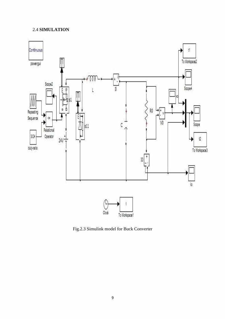
2.4 SIMULATION
Fig.2.3 Simulink model for Buck Converter

10
2.4.1 RESULTS AND DISCUSSION
Fig 2.4 Capacitor voltage
Fig 2.5 Inductor current
Fig 2.6 Output voltage

11
Summary
From the response obtained in MATLAB/Simulink the overshoot of output
voltage is 73.3% and rise time is 0.162 milliseconds .The settling time is 18
milliseconds. As overshoot, rise time and settling times are too high ,to minimise it
different controllers are used.
12
CHAPTER-3
ANALYSIS OF BUCK CONVERTER OUTPUT WITH DIFFERENT
CONTROLLER
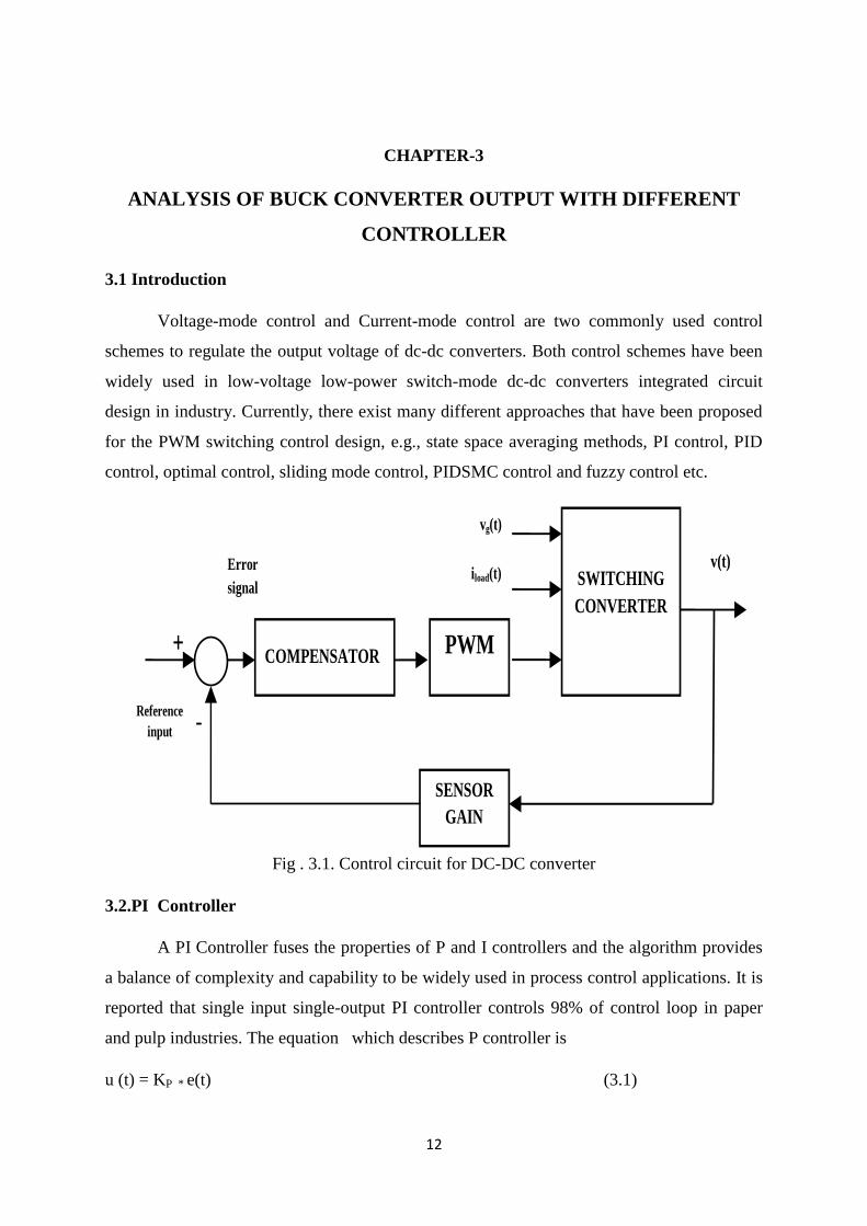
3.1 Introduction
Voltage-mode control and Current-mode control are two commonly used control
schemes to regulate the output voltage of dc-dc converters. Both control schemes have been
widely used in low-voltage low-power switch-mode dc-dc converters integrated circuit
design in industry. Currently, there exist many different approaches that have been proposed
for the PWM switching control design, e.g., state space averaging methods, PI control, PID
control, optimal control, sliding mode control, PIDSMC control and fuzzy control etc.
SWITCHING
CONVERTER
PWM COMPENSATOR
SENSOR
GAIN
Reference
input
Error
signal
vg(t)
iload(t) v(t)
+
-
Fig . 3.1. Control circuit for DC-DC converter
3.2.PI Controller
A PI Controller fuses the properties of P and I controllers and the algorithm provides
a balance of complexity and capability to be widely used in process control applications. It is
reported that single input single-output PI controller controls 98% of control loop in paper
and pulp industries. The equation which describes P controller is
u (t) = KP * e(t) (3.1)

13
whereKpis proportional gain, e (t) is the error and u(t) is the perturbation in output signal of
PI controller from the base value corresponding to normal operating conditions. It with no
integration property always exhibit static error in the presence of disturbances and changes in
set-point and shows a relatively maximum overshoot and long settling time as shown in
Figure 6. To remove steady-state offset in controlled variable of a process, an extra
intelligence is added to the P controller and this intelligence is t integral action. The controller
is a PI controller whose mathematical notation is depicted in equation.
( ) * ( )
∫ ( )
+ (3.2)
3.2.1.BUCK CONVERTER WITH PI CONTROLLER
Fig.3.2. Simulink Diagram for Buck Converter with PI controller

14
Fig3.2.2 Output voltage with PI controller
Fig 3.2.3 Output current with pi controller
From the response obtained in MATLAB/Simulink the overshoot of output
voltage is 227% and rise time is 0.056 milliseconds .The settling time is 1.1
milliseconds. As overshoot is too high ,to minimise it another controller (PID) is used.
0 0.01 0.02 0.03 0.04 0.05 0.06 0.07 0.08 0.09 0.10
0.2
0.4
0.6
0.8
1
1.2
1.4
1.6
1.8
2
time in second
curr
ent
in a
mpe
re
output current of buck converter with PI controller
Kp= 1.314Ki=33.964
0 0.01 0.02 0.03 0.04 0.05 0.06 0.07 0.08 0.09 0.10
1
2
3
4
5
6
7
8
9
10
time in second
outp
ut
vo
lta
ge
in
volt
s
output voltage of buck converter with PI controller
Kp=1.314Ki= 33.964

15
3.3 PID controller
A proportional-integral-derivative controller (PID controller) is a generic control loop
feedback mechanism widely used in industrial control systems. A PID controller attempts to
correct the error between a measured process variable and a desired set point.
The PID controller calculation (algorithm) involves three separate parameters; the
Proportional, the Integral and Derivative values. The Proportional value determines the
reaction to the current error, the Integral determines the reaction based on the sum of recent
errors and the Derivative determines the reaction to the rate at which the error has been
changing. The weighted sum of these three actions is used to adjust the process via a control
element such as the position of a control valve or the power supply of a heating element. By
"tuning" the three constants in the PID controller algorithm the PID can provide control
action designed for specific process requirements. The response of the controller can be
described in terms of the responsiveness of the controller to an error, the degree to which the
controller overshoots the set-point and the degree of system oscillation. Note that the use of
the PID algorithm for control does not guarantee optimal control of the system.
3.3.1Proportional term
The proportional term makes a change to the output that is proportional to the current
error value. The proportional response can be adjusted by multiplying the error by a constant
Kp, called the proportional gain.
The proportional term is given by:
( )(3.3)
Where
Pout: Proportional output
Kp: Proportional Gain, a tuning parameter
• e: Error = SP − PV
• t: Time or instantaneous time (the present)
A high proportional gain results in a large change in the output for a given change in
the error. If the proportional gain is too high, the system can become unstable (See the section

16
on Loop Tuning). In contrast, a small gain results in a small output response to a large input
error, and a less responsive (or sensitive) controller. If the proportional gain is too low, the
control action may be too small when responding to system disturbances. In the absence of
disturbances pure proportional control will not settle at its target value, but will retain a
steady state error that is a function of the proportional gain and the process gain. Despite the
steady-state offset, both tuning theory and industrial practice indicate that it is the
proportional term that should contribute the bulk of the output change.
3.3.2 Integral term
The contribution from the integral term is proportional to both the magnitude of the
error and the duration of the error. Summing the instantaneous error over time (integrating
the error) gives the accumulated offset that should have been corrected previously. The
accumulated error is then multiplied by the integral gain and added to the controller output.
The magnitude of the contribution of the integral term to the overall control action is
determined by the integral gain, Ki.
The integral term is given by:
∫ ( )
(3.4)
Where
Iout: Integral output
Ki: Integral Gain, a tuning parameter
Error = SP − PV
τ: Time in the past contributing to the integral response
The integral term (when added to the proportional term) accelerates the movement of
the process towards set point and eliminates the residual steady-state error that occurs with a
proportional only controller. However, since the integral term is responding to accumulated
errors from the past, it can cause the present value to overshoot the setpoint value (cross over
the set point and then create a deviation in the other direction). For further notes regarding
integral gain tuning and controller stability, see the section on Loop Tuning.

17
3.3.3 Derivative term
The rate of change of the process error is calculated by determining the slope of the
error over time (i.e. its first derivative with respect to time) and multiplying this rate of
change by the derivative gain Kd. The magnitude of the contribution of the derivative term to
the overall control action is determined the
(3.5)
Where
Dout: Derivative output
Kd: Derivative Gain, a tuning parameter
e: Error = SP − PV
t: Time or instantaneous time (the present)
The derivative term slows the rate of change of the controller output and this effect is
most noticeable close to the controller setpoint. Hence, derivative control is used to reduce
the magnitude of the overshoot produced by the integral component and improve the
combined controller-process stability. However, differentiation of a signal amplifies noise in
the signal and thus this term in the controller is highly sensitive to noise in the error term, and
can cause a process to become unstable if the noise and the derivative gain are sufficiently
large. The output from the three terms, the proportional, the integral and the derivative terms
are summed to calculate the output of the PID controller.
First estimation is the equivalent of the proportional action of a PID controller. The
integral action of a PID controller can be thought of as gradually adjusting the output when it
is almost right. Derivative action can be thought of as making smaller and smaller changes as
one gets close to the right level and stopping when it is just right, rather than going too far.
Making a change that is too large when the error is small is equivalent to a high gain
controller and will lead to overshoot. If the controller were to repeatedly make changes That
were too large and repeatedly overshoot the target, this control loop would be termed
unstable and the output would oscillate around the setpoint in a either a constant, a growing

18
or a decaying sinusoid. A human would not do this because we are adaptive controllers,
learning from the process history, but PID controllers do not have the ability to learn and
must be set up correctly. Selecting the correct gains for effective control is known as tuning
the controller.
If a controller starts from a stable state at zero error (PV = SP), then further changes
by the controller will be in response to changes in other measured or unmeasured inputs to
the process that impact on the process, and hence on the PV. Variables that impact on the
process other than the MV are known as disturbances and generally controllers are used to
reject disturbances and/or implement set point changes.
In theory, a controller can be used to control any process which has a measurable
output (PV), a known ideal value for that output (SP) and an input to the process (MV) that
will affect the relevant PV. Controllers are used in industry to regulate temperature, pressure,
flow rate, chemical composition, level in a tank containing fluid, speed and practically every
other variable for which a measurement exists. Automobile cruise control is an example of a
process outside of industry which utilizes automated control. Kp: Proportional Gain - Larger
Kp typically means faster response since the larger the error, the larger the feedback to
compensate. An excessively large proportional gain will lead to process instability. Ki:
Integral Gain - Larger Ki implies steady state errors are eliminated quicker. The trade-off is
larger overshoot: any negative error integrated during transient response must be integrated
away by positive error before we reach steady state. Kd: Derivative Gain - Larger Kd
decreases overshoot, but slows down transient response and may lead to instability.
3.3.4 Loop tuning
If the PID controller parameters (the gains of the proportional, integral and derivative
terms) are chosen incorrectly, the controlled process input can be unstable, i.e. its output
diverges, with or without oscillation, and is limited only by saturation or mechanical
breakage. Tuning a control loop is the adjustment of its control parameters (gain/proportional
band, integral gain/reset, derivative gain/rate) to the optimum values for the desired control
response.
Some processes must not allow an overshoot of the process variable beyond the set
point if, for example, this would be unsafe. Other processes must minimize the energy
expended in reaching a new setpoint. Generally, stability of response (the reverse of
instability) is required and the process must not oscillate for any conditions or set points.

19
Some processes have a degree of non-linearity and so parameters that work well at full-load
conditions don't work when the process is starting up from no-load. This section describes
some traditional manual methods for loop tuning.
There are several methods for tuning a PID loop. The most effective methods
generally involve the development of some form of process model, and then choosing P, I,
and D based on the dynamic model parameters. Manual "tune by feel" methods have proven
time and again to be inefficient, inaccurate, and often dangerous.
The choice of method will depend largely on whether or not the loop can be taken
"offline" for tuning, and the response time of the system. If the system can be taken offline,
the best tuning method often involves subjecting the system to a step change in input,
measuring the output as a function of time, and using this response to determine the control
parameters
Fig.3.3.1 MATLAB/Simulink model of Buck Converter with PID controller
1
Out1
Continuous
powergui
3
Vo_ref
t
To Workspace1
Vo
To Workspace
Subtract
In2 Out1
Subsystem
Step Response
Specifications
Scope
eu
PID Controller
Clock

20
(a)
(b)
(c )
Fig 3.3.2. Buck converter responses with PID controller
(a) Capacitor voltage
(b) Inductor current
(c) Output voltage

21
From the response obtained in MATLAB/Simulink the overshoot of output
volage is 213% and rise time is 0.047 milliseconds .The settling time is 0.6
milliseconds.As overshoot is too high ,to minimise it another controller (SMPID) is
used.
3.4 SLIDING MODE PID CONTROLLER
Sliding mode control (SMC) for DC/DC converters is a topic that has been covered in
numerous publications during the last decade. Originating from the control engineering field
sliding mode techniques are well described and many advanced implementations are possible.
For most DC/DC applications, low controller complexity is desirable (to reduce cost and
simplify design and implementation), and generally, simple control schemes such as PD or
PID voltage-mode are preferable. The sliding mode PID voltage controller is particularly
useful, due to its high performance and simple implementation. To increase the applicability
of the solution, proper modelling tools are needed so that the closed-loop control system
performance can be predicted, analysed and optimized.
Designing of Sliding mode is based on three conditions.
0 0.01 0.02 0.03 0.04 0.05 0.06 0.07 0.08 0.09 0.10
0.5
1
1.5
Time (s)
Cu
rren
t (A
)Output current
Fig3.3.3 Output current

22
Existence Condition.
Reaching Condition.
Stability Condition.
Existence conditions.
The trajectory is required either to slide or switch after reaching the switching
function.
The existence condition for SMC
(3.6)
(3.7)
Reaching conditions.
Design the switching function in such a way that our initial equilibrium point
will reach the switching trajectory.
System: ( )
( )
( ) (3.8)
Sufficient reaching condition
( )
( )
u = Scalar discontinuous function
X = steady state representative point
+ = positive surface
- = negative surface

23
Fig3.4.1 Derived model of a sliding mode PID voltage-mode control system for a buck
converter[23].
To simplify analysis the PID compensator is considered as cascaded PD and PI
compensators. For the PD compensated buck converter output voltage, following relationship
is found
( ) ( )
( )
(3.9)
Using the basic description of a capacitor and Kirchoff’s current law leads to
[ ]
(3.10)
This suggests that the PD compensated buck converter output voltage feedback
system is functionally equivalent to a full state-feedback control system with ideal output
current feed-forward compensation (as illustrated in above figure) – the output current is fed
back with equal gain but opposite polarity compared to the inductor current. Using the
constants given in Table 1, this can be rewritten to:
( ) (3.11)
V ref K rff
K vfb
K cfb
K I
K P
s
1
K cff
V PIint,
V carrier
V PDout ,)(
V PWM
L
C
I L
V S
I outV out I load
I pert

24
The PI part of the compensator introduces an extra state to the system, the output of
the integrator part, vint,PI is chosen for this state. The relationship between input and output of
the PI compensator is:
( )
(
)(3.12)
The integrator output is then given by:
(3.13)
This leads to the following state equation for vint,PI
( 3.14)
The found expressions for the constants in the PID controller equivalent model are
listed in Table 2
Parameter Expression
Output voltage feedback gain Kvfb
Inductor current feedback gain Kcfb
Output current feed-forward gain Kcff
Reference summation gain Krff
PI compensator proportional gain KP 1
PI compensator integral gain KI
Table 3.1 Gains in PID controller equivalent model [23]
To demonstrate the performance of the proposed dc-dc buck converter using sliding
mode PID controller in MATLAB/Simulink with the parameters as given in Table 3. A

25
constant voltage source of 30 V is input to the converter with R load having the value R
=1KΩ, . The complete model consists of a voltage source, a linear load, a voltage source
PWM converter.
COMPONENTs PARAMETERs VALUE IN PROTOTYPE
Output inductor L 10 µH
Output capacitance C 0.99 µF
Inductor/switch series R RS 100 mΩ
Total time delay td 60 ns
PID component Rd 10 kΩ
PID component Cd 180 pF
PID component RPI 1 kΩ
PID component CPI 10 nF
Ref. injection resistor RRFF 1kΩ
Table 3.2 SMC PID buck prototype design parameters[23]
Fig3.4.2 Block diagram of sliding mode PID voltage-mode control system for a buck
converter.

26
RESULTS
Fig 3.4.3.Output voltage with SMPID controller
Fig 3.4.4 Inductor current with SMPID controller
Fig3.4.5Capacitor voltage with SMPID controller
From the response obtained in MATLAB/Simulink the overshoot of output
volage is 0.08% and rise time is 0.01 milliseconds .The settling time is 0.01
0 0.002 0.004 0.006 0.008 0.01 0.012 0.014 0.016 0.018 0.020
2
4
6
8
10
12
14
16
Time in seconds
Ou
tpu
t v
olt
age
in v
olt
s
Output voltage of buck converter using SMPID
0 0.002 0.004 0.006 0.008 0.01 0.012 0.014 0.016 0.018 0.020
2
4
6
8
10
12
14
16
Time in seconds
Cap
acit
or
vo
ltag
e i
n v
olt
s
Capacitor voltage of buck converter with SM PID
0 0.002 0.004 0.006 0.008 0.01 0.012 0.014 0.016 0.018 0.020
0.5
1
1.5
2
2.5
3
3.5
4
Time in seconds
Ind
uct
or
curr
ent
in a
mp
eres
Inductor current of buck converter with SMPID
27
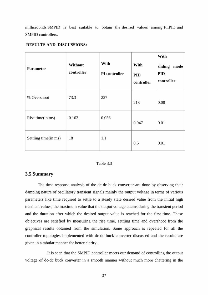
milliseconds.SMPID is best suitable to obtain the desired values among PI,PID and
SMPID controllers.
RESULTS AND DISCUSSIONS:
Parameter Without
controller
With
PI controller
With
PID
controller
With
sliding mode
PID
controller
% Overshoot 73.3 227
213
0.08
Rise time(in ms) 0.162
0.056
0.047
0.01
Settling time(in ms) 18 1.1
0.6
0.01
Table 3.3
3.5 Summary
The time response analysis of the dc-dc buck converter are done by observing their
damping nature of oscillatory transient signals mainly the output voltage in terms of various
parameters like time required to settle to a steady state desired value from the initial high
transient values, the maximum value that the output voltage attains during the transient period
and the duration after which the desired output value is reached for the first time. These
objectives are satisfied by measuring the rise time, settling time and overshoot from the
graphical results obtained from the simulation. Same approach is repeated for all the
controller topologies implemented with dc-dc buck converter discussed and the results are
given in a tabular manner for better clarity.
It is seen that the SMPID controller meets our demand of controlling the output
voltage of dc-dc buck converter in a smooth manner without much more chattering in the

28
transient period by decreasing the rate of transition between the states of high frequency
oscillation and low frequency steady state value and thereby shows a sharp decrease in rise
time and settling time. The implementation of SMPID controller also reduces the unwanted
peak of output voltage during the transient period almost to zero and therefore reduces the
chances of damage due to sudden rise of voltage in modern day power electronic devices
having a very narrow tolerance zone to meet the requirements ultrafast performance.

29
4.1 Design Concept
The project design constraints on power efficiency, lower cost, and less reduce space
and components used. For higher power application, power supplies that need to provide
higher current not suitable use to the chip since the current is too high for handled and it
might cause IC damage. And therefore it may cause instability condition when the load or
input voltage changing may cause system at risk. Dynamic power losses are due to the
switching behavior of the selected pass devices (MOSFETs, Power Transistors, IGBTs, etc.).
These losses include turn-on and turn-off switching losses and switch transition losses. Since
an increasing of power electronics circuits in many applications such used in automobiles to
laptops which use an integrated circuit (IC) and form in smaller size. The lower system cost
improvement of power supply show in designing of power supplies using analogue
techniques requires components to be oversized to compensate for component variation and
component drift. Using analog circuitry to implement system control functions is not always
cost-effective or flexible. Losses in an electric or power electronics circuits come from many
source, in this project the losses such a resistive losses in the controllable switch, capacitive
losses due to charging of the controllable gates and parasitic capacitances, short circuit
current through the controllable switch especially current flow during switch open and
voltage drop across when switch is closed and the parasitic losses of filter in an inductor and
capacitor. More that, in order to regulate the output voltage, the duty cycle to the buck
converter is set by a feedback control loop, but to associate the controller design to buck
converter power elements, it may cause inefficient in power conversion. To ensure the
systemstability and for improving transient output response, the more complex proportional
integral derivative (PID) controller can be implemented.
4.2 Components Review
4.2.1 Bridge rectifier
In order to produces unregulated dc supply voltage up to 15Vdc from main supply of
240Vac, this silicon bridge rectifier is used to the circuit. The cost of this component is cheap
with the features maximum average forward output current.

30
4.2.2Opto-isolator IC (TLP 250)
The opto-isolator is used to convert the voltage mode (output voltage) read from Buck
converter to an appropriate value of gate pulse of 50KHz,5Vto perform closed loop feedback
conversion system in order to maintain output voltage at desired level. The data sheet is given
in the appendix A.
4.2.3 MOSFET
SMPS MOSFET has limitations operation in terms of voltage, current and power
dissipation. The power absorbed by the gate drive circuitry should not significantly affect the
overall efficiency. The power MOSFET current rating is related with the heat dissipated in
the devices. This rating will be take in consideration for designing appropriate circuit to
protect power MOSFET against high voltage and current, thus cause heat generation. While
considering protection of power MOSFET against over voltage, a distinction has to be made
between slowly varying over voltage and short time surge. It is about 100Vdc the minimum
rating of drain to source breakdown voltage. Gate voltage must be 10-25V higher than the
drain voltage. Being a high side switch, such gate voltage would have to be higher than the
rail voltage, which is frequently the higher voltage available in the system. The data sheet is
given in the appendix B.
Fig.4.1 Pin Configuration of TLP 250
1. NC
2. Anode
3. Cathode
4. NC
5. Ground
6. Vo(OUTPUT)
7. Vo(OUTPUT
8. VCC

31
4.2.4 Capacitor
The capacitor is chosen with minimum loss because switched power regulators are
usually used in high current-performance power supplies. Loss occurs because of its internal
series resistance and inductance. Commonly capacitors for switched regulators are chosen
based on the equivalent series resistance (ESR).
The capacitance of the capacitor (C) is given by
( )
(4.1)
4.2.5 Inductor
The function on inductor is to store energy and the value is selected to maintain a
continuous current mode (CCM) operation as a rated of load (5 Ω) is decided for this Buck
converter. In CCM, current flow continuously in inductor during the entire switching cycle
and output inductance selected to limit the peak to peak ripple current flowing. The factors
tobe considered in selecting the inductor are its peak to peak ripple current (CCM), maximum
dc or peak current (not overheat) and maximum operating frequency (maximum core loss is
not exceeded, resulting in overheating or saturation).
The inductance of the inductor (L) is given by
( )
(4.2)
Fig.4.2 Pin Configuration of IRF 540
1. Gate
2. Drain
3. Source

32
4.2.6 PIC microcontroller
The microcontroller selected to control the closed –loop feedback conversion power
was the 40-pin PDPIP package of the PIC30F4011. The pin configuration is given in Fig 5.3.
A primary benefit of this microcontroller is the flexibility of the many I/O pins to
accommodate analog to digital signals other than easy to firm the program.
40
39
38
37
36
35
34
33
32
31
30
29
28
27
26
25
24
23
22
21
-
-
-
-
-
-
-
-
-
-
-
-
-
-
-
-
-
-
-
-
0
1
2
3
4
5
6
7
8
9
10
11
12
13
14
15
16
17
18
19
20
-
-
-
-
-
-
-
-
-
-
-
-
-
-
-
-
-
-
-
-
-
PIC
30F
4011
AVDD
AVSS
PWM1L/RE0
PWM1H/RE1
PWM2L/RE2
PWM2H/RE3
PWM3L/RE4
PWM3H/RE5
VDD
VSS
C1RX/RF0
C1TX/RF1
U2RX/CN17/RF4
U2TX/CN18/RF5
PGC/EMUC/U1RX/SDI1/SDA/RF2
PGD/EMUD/U1TX/SDO1/SCL/RF3
SCK1/RF6
EMUC2/UC1/IC1/INT1/RD0
OC3/RD2
VDD
MCLR
EMUD3/AN0/VREF+/CN2/RB0
EMUC3/AN1/VREF-/CN3/RB1
AN2/SS1/CN4/RB2
AN3/IND/CN5/RB3
AN4/QEA/ICT/CN6/RB4
AN5/QEB/IC8/CN7/RB5
AN6/OCFA/RB6
AN6/RB7
AN8/RB8
VDD
VSS
OSC1/CLK1
OSC2/CLK0/RC15
EMUD1/SOSC1/T2CK/U1ATX/CN1/RC13
EMUC1/SOSC0/T1CK/U1ARX/CN0/RC14
FLTA/INTO/RE8
EMUD2/OC2/IC2/INT2/RD1
OC4/RD3
VSS
Fig. 4.3 Pin configuration of PIC30F4011

33
4.3 PID BASED MICROCONTROLLER
This Buck system is closed loop feedback system, in order to simulate or to firm the
program for controller, the basic such Proportional Error Gain (P-Gain) which this parameter
produces a correction factor that is proportional to the magnitude of the output voltage error,
an integral error gain (I-Gain) which this parameter uses the cumulative voltage error to
generate a correction factor that eliminates any residual error due to limitations in offset
voltages and measurement resolution an Derivative error gain (D-Gain) which this
parameters produces a correction factor that is proportional to the rate of change of the output
error voltage, which helps the system respond quickly to changes in the system conditions.
Feed forward gain – this parameter produces a correction factor that is computed based on the
magnitude of the input voltage, inductor current and circuit attributes such an inductor and
capacitor value. Thistermallow the control loop to be protective rather than reactive. In other
words, when the input voltage changes, feed forward gain responds so that the control loop
does not have to wait until the output voltage changes before making the appropriate gain
correction. Using the PID algorithm, the proportional,integral and derivative error of the
actual versus the desired output voltage is combined to control the PWM duty cycle. The PID
algorithm will be used in voltage mode control loops. The PID software is typically small,
but its execution rate is very high, often hundreds of thousands of iterations per second. This
highiteration raterequires the PID software routine be as efficient as possible to minimize
performance. The PID control-loop is interrupt-driven by the ADC on a fixed-time basis. Any
system function that can be executed in the “idle loop” should be, in order to reduce the
unnecessary workload within the PID control software. Functions such as voltage ramp
up/down, error detection, feed-forward calculations and communication support routines are
candidates for the idle loop. Any other interrupt-driven processes, such as communication,
must beat lower priority than the PID loop.
4.3.1 Voltage –mode control
Voltage-mode control is the methods of control based on analog switch-mode power
supply (SMPS) control techniques. In voltage mode, the difference between desired and
actual output voltage (error) controls the time that the supply voltage is applied across the
inductor, which indirectly controls current flow in the inductor. Varying the duty cycle
essentially adjusts the input voltage drive to the Buck's LC components which directly

34
effects. Voltage-mode can provide more stability in a noisy environment and over a wide
operating range.
4.4 PIC Microcontroller Tools Development
4.4.1Picbasic pro compiler (pbp)
P CBAS C PRO™ Compiler is the easiest way to program the fast and powerful
Microchip Technology PIC microcontrollers (PIC30F4011). PICBASIC PRO converts
BASIC programs into files that can be programmed directly into a PIC MCU. The BASIC
language is much easier to read and write than the quirky Microchip assemblylanguage. PBP
compiler produces code that may be programmed into a wide variety of PIC microcontroller
having from 8 up to 84 pins and various on-chipfeatures including A/D converters, hardware
timers and serialports. The PIC30F4011 use Harvard technology to allow rapid erasing and
reprogramming for program debugging. The PIC30F4011 devices also contain between 64
and 1024 bytes ofnon-volatile data memory that can be used to store program and data and
other parameters even when the power is turned off.
4.4.2 Window interface software
Mplab is actually Integrated Development Environment (IDE) with In Circuit
Debugging (ICD) capability designed specifically for PICBASIC PRO compiler. This
software is easy to set up and capable to identify, correct the compilation and assembler an
error. The controller algorithm programming writtenin Mplab..
4.4.3 Programming Adapters and mplabs U2 pic programmer
The melabs U2 PIC Programmer is driven and powered from a single USB port on
computer. Then adapters connect the programmer's 40-pin expansion header to allow
programming of PIC microcontrollers in DIP, PLCC or surface mount packages.

35
Figure 4.4: Mp lab SCREENSHOTS
METHODOLOGY
4.5 Introduction
This chapter explains about hardware development such as equipments, procedures
and method design for Buck converter including controller technique used in closed-loop
feedback system. This chapter also explains about the software interface and the complete
operation of the Buck converter. Before looking at the details of all methods below, it is good
to begin with brief review of the problem that is considered in this Buck converter. The
changing of voltage from input supply will be consider as problem need to against by apply
feedback controller in order to maintain an output from Buck converter.

36
4.5.2 Hardware Development
4.5.3 Circuit function
Figure 4.5:Design flow for Microcontroller Based Buck PID system
In the hardware part, the circuit is design to step down dc – to – dc voltage. The
circuit included parts of Buck components such as controllable switch (IRF540), inductor and
capacitor, PIC30F4011microcontroller, optoisolator (TLP250), and other basic components.
Rectifier and filter circuit is design to obtain voltage up to 15Vdc from main source. The
voltage obtained will be step down by Buck converter to 3Vdc. In order to maintain output
voltage, controller will be operated infeedback circuit. The complete circuit for the system is
shown in APPENDIX I. PIC30F4011 is used to control SMPSMOSFET switching duty cycle
which is connected to Buck converter circuit.PIC30F4011has 40 pins. Since the PWM that
will be apply to Buck converter is varied in order to maintain the output voltage, the HPWM
function pin at RC2/CCP1/P1A need to set in order to generate the PWM signal from the
microcontroller. The 20MHz crystal oscillator is used for PIC30F4011 microcontroller
internal clock.
4.5.4 Basic Buck converter circuit operation
Figure 4.5 show the full Buck converter equivalent circuit. For determining the output
voltage of Buck converter, the inductor current and inductor voltage should be examined
first. Observations made during controllable switch closed and switch open.

37
Fig4.6 buck converter
Refer on Figure 4.6, when the duty cycle is in ON state, diode become as reversed biased and
the inductor will deliver current and switch conducts inductor current. With the voltage (Vin -
Vo) across the inductor, the current rises linearly (current changes, ∆i ). The current through
the inductor increase, as the source voltage would be greater then the outputvoltage and
capacitor current may be in either direction depending on the inductor current and load
current. When the current in inductor increase, the energy stored also increased. In this state,
the inductor acquires energy. Capacitor will provides smooth out of inductor current changes
into a stable voltage at output voltage and it’s big enough such that V out doesn’t change
significantly during one switching cycle.
InOFF state of duty cycle, the diode is ON and the inductor will maintains current to
load. Because of inductive energy storage, iL will continues to flow. While inductor releases
current storage, it will flow to the load and provides voltage to the circuit. The diode
isforward biased. The current flow through the diode which is inductor voltage is equal with
negative output voltage. The model is shown in fig 4.7
R1 R2
R3

38
Fig 4.7 model of buck converter with microcontroller
The output voltage is obtained using DSO in open loop and closed loop mode
with microcontroller controlled in PID logic.
a)
b )

39
c)
Fig 4.8. Responses of buck converter obtained from microcontroller implemented PID
controller.
a)output voltage in open loop
b)output voltage in closed loop
c)capacitor voltage in closed loop

40
4.6 RESULTS AND DISCUSSIONS
Parameter
With
microcontroller
Implemented PID
controller
With
PID controller
With
sliding mode PID
controller
% Overshoot 0
213
0.08
Rise time(in ms) 0.027
0.047
0.01
Settling time(in ms) 0.35
0.6
0.01
Table 4.1
It is observed that the output voltage has overshoot 0f around 6% with a
settling time of around 420 microseconds in open loop. But in closed loop when it is
controlled by microcontroller with PID as base, overshoot reduces to zero and settling
time falls to around 350 microseconds.

41
4.7 CONCLUSIONS
The time response analysis of the dc-dc buck converter are done by observing their
damping nature of oscillatory transient signals mainly the output voltage in terms of various
parameters like time required to settle to a steady state desired value from the initial high
transient values, the maximum value that the output voltage attains during the transient period
and the duration after which the desired output value is reached for the first time. These
objectives are satisfied by measuring the rise time, settling time and overshoot from the
graphical results obtained from the simulation. Same approach is repeated for all the
controller topologies implemented with dc-dc buck converter discussed and the results are
given in a tabular manner for better clarity.
It is seen that the SMPID controller meets our demand of controlling the
output voltage of dc-dc buck converter in a smooth manner without much more chattering in
the transient period by decreasing the rate of transition between the states of high frequency
oscillation and low frequency steady state value and thereby shows a sharp decrease in rise
time and settling time. The implementation of SMPID controller also reduces the unwanted
peak of output voltage during the transient period almost to zero and therefore reduces the
chances of damage due to sudden rise of voltage in modern day power electronic devices
having a very narrow tolerance zone to meet the requirements ultrafast performance.
FUTURE SCOPE :
Design and implementation of SMC and SMPID with microcontroller in
the designed buck converter for voltage mode control and to observe the
chattering during transient state.

42
REFERENCES:
[1] M. H. Rashid, “Power Electronics, Circuits, Devices And Applications,” 2nd ed. Englewood Cliffs, NJ:
Prentice Hall, 1993.
[2] R. W. Erickson, “Fundamentals of Power Electronics” Norwell, MA: Kluwer-Academic.1999
[3] Mohan, Undeland, Riobbins, Power Electronics Converters Applications and Design, 3rd edition,
Wiley India (P.) Ltd.
[4] R.D Middlebrook and S Cuk , “A general unified approach to modelling switching Converter Power
stages,” in Proc. IEEE PESC Rec., pp. 18–34, 1976.
[5] A.J. Forsyth and S.V. Mollow, “Modelling and control of dc-dc converters,” IEE power engineering
journal, vol. 12, no. 5, pp. 229–236, Oct. 1998.
[6] V.S.C Raviraj and P.C. Sen, “Comparative Study of proportional-integral, Sliding-mode, and fuzzy logic
controllers for power converters,” IEEE transaction on Industry applications, vol. 33, no. 2, pp. 518-
524, Mar. /Apr. 1997.
[7] Kapat, S.; Krein, P.T.; , "Formulation of PID control for dc-dc converters based on capacitor current: A
geometric context," Control and Modelling for Power Electronics (COMPEL), 2010 IEEE 12th
Workshop on , vol., no., pp.1-6, 28-30 June 2010
[8] R. Anandanatarajan, P. Ramesh Babu, Control System Engineering, 3rd edition, SciTech Publications
(India) Pvt. Ltd.
[9] Stanislaw H. Zak,Systems and Control, Oxford University Press, New York, 2003.
[10] Juing-Huei Su; Jiann-Jong Chen; Dong-Shiuh Wu; , "Learning feedback controller design of switching
converters via MATLAB/SIMULINK," Education, IEEE Transactions on , vol.45, no.4, pp. 307- 315, Nov
2002.
[11] Escobar, G.; Ortega, R.; Sira-Ramirez, H.; Vilain, J.P.; Zein, I.; , "An experimental comparison of
several nonlinear controllers for power converters," Decision and Control, 1997., Proceedings of the
36th IEEE Conference on , vol.1, no., pp.227-228 vol.1, 10-12 Dec 1999.
[12] Ang, S.S.; , "A practice-oriented course in switching converters," Education, IEEE Transactions on ,
vol.39, no.1, pp.14-18, Feb 1996.
[13] Fliess, M.; , "Generalized controller canonical form for linear and nonlinear dynamics," Automatic
Control, IEEE Transactions on , vol.35, no.9, pp.994-1001, Sep 1990.
[14] Siew-Chong Tan; Lai, Y.M.; Tse, C.K.; Cheung, M.K.H.; , "An adaptive sliding mode controller for buck
converter in continuous conduction mode," Applied Power Electronics Conference and Exposition,
2004. APEC '04. Nineteenth Annual IEEE , vol.3, no., pp. 1395- 1400 Vol.3, 2004
[15] Shoei-Chuen Lin; Ching-Chih Tsai; , "Adaptive voltage regulation of PWM buck DC-DC converters
using back stepping sliding mode control," Control Applications, 2004. Proceedings of the 2004 IEEE
International Conference on , vol.2, no., pp. 1382- 1387 Vol.2, 2-4 Sept. 2004
[16] Algreer, Maher; Armstrong, Matthew; Giaouris, Damian; , "Adaptive control of a switch mode dc-dc
power converter using a Recursive FIR predictor," Power Electronics, Machines and Drives (PEMD
2010), 5th IET International Conference on , vol., no., pp.1-6, 19-21 April 2010
[17] Jafari, M.; Malekjamshidi, Z.; , "Design, Simulation and implementation of an adaptive controller on
base of artificial neural networks for a resonant DC-DC converter," Power Electronics and Drive
Systems (PEDS), 2011 IEEE Ninth International Conference on , vol., no., pp.1043-1046, 5-8 Dec. 2011

43
[18] Zhou Wei; Liu Bao-bin; , "Analysis and design of DC-DC buck converter with nonlinear adaptive
control," Computer Science & Education (ICCSE), 2012 7th International Conference on , vol., no.,
pp.1036-1038, 14-17 July 2012
[19] Mattavelli, P.; Rossetto, L.; Spiazzi, G.; , "Small-signal analysis of DC-DC converters with sliding mode
control ," Applied Power Electronics Conference and Exposition, 1995. APEC '95. Conference
Proceedings 1995., Tenth Annual , vol., no.0, pp.153-159 vol.1, 5-9 Mar 1995
[20] Siew-Chong Tan; Lai, Y.M.; Cheung, M.K.H.; Tse, C.K.; , "On the practical design of a sliding mode
voltage controlled buck converter," Power Electronics, IEEE Transactions on , vol.20, no.2, pp. 425-
437, March 2005
[21] Fossas, E.; Olm, J.M.; , "Generation of signals in a buck converter with sliding mode control ," Circuits
and Systems, 1994. ISCAS '94., 1994 IEEE International Symposium on , vol.6, no., pp.157-160 vol.6,
30 May-2 Jun 1994
[22] Hongmei Li; Xiao Ye; , "Sliding-mode PID control of DC-DC converter," Industrial Electronics and
Applications (ICIEA), 2010 the 5th IEEE Conference on , vol., no., pp.730-734, 15-17 June 2010.
[23] Mikkel C. W. Høyerby ;Michael A. E. Andersen ,”Accurate Sliding-Mode Control System Modeling for
Buck Converters”to be presented at PESC2007, June 2007
[24] V. Utkin, J. Guldner, J. Shi, ”Sliding Model Control in Electromechanical Systems”, CRC Press, 1999
[25] Chung-HsienTso, Jiiin-Chuan Wu, “A Ripple Controlled Buck Regulator With Fixed Output
Frequency”, IEEE Power Electronics Letters, vol. 1, no. 3, September 2003
[26] SørenPoulsen, Michael A. E. Andersen, ”Simple PWM modulator with excellent dynamic behaviour”, proc. of APEC 2004, February 2004, Anaheim, USA, pp 486-492
[27] SørenPoulsen, “Global loop integrating modulator”, WO2004100356-A2, patent application
[28] M. C. W. Høyerby, M. A. E. Andersen, “Ultra-Fast Tracking Power Supply with 4th order Output Filter and Fixed-Frequency Hysteretic Control”, to be published
[29] M. C. W. Høyerby, M. A. E. Andersen, “A small-signal model of the hysteretic comparator in linearcarrier self-oscillating switch-mode controllers”, proc. of NORPIE 2006, Lund, Sweden, June 2006
[30] Gene W. Wester, “Describing-function analysis of a ripple regulator with slew-rate limits and time delays”, proc. of PESC 1990, June 1990, pp 341-346
[31] O. Rafael, S. Daniel, K. Charif, “Simple Hysteresis Describing Technique to Control a Non-Active Power Compensator”, proc. of PESC 2005, June 2005, pp 1732-1737
[32] Thomas H. Lee, “The Design of CMOS Radio-Frequency Integrated Circuits”, 2nd edition, Cambridge University Press, 2004, pp 617-620
[33] E. Fossas, J. P. Olm, “Generation of Signals in a Buck Converter with Sliding Mode Control”, proc. Of ISCAS ’94, May 2004, pp 157-160
[34] M. C. W. Høyerby, M. A. E. Andersen, “A Comparative Study of Analog Voltage-mode Control
Methods for Ultra-fast Tracking Power Supplies”, to be presented at PESC2007, June