Embed Size (px)
Citation preview
Unconventional Systems Integration
E. Williams, Chair W. Dally
A. Despain D. Eardley
D. Hammer P. Horowitz
]. Katz N. Lewis
J. Sullivan R. Westervelt
May 1996
]SR-95-120
Approved for Public Release. Distribution Unlimited.
JASON The MITRE Corporation
1820 Dolley Madison Boulevard Mclean, Virginia 22102-3481
(703) 883-6997
,...--....,:,oo'-"'=-~~~;t.o~~ ........ ,lJ."~ ...... " ..... _~.......w.
'. ,PA~"!lIFI.J1."IOw lli'l~>':1'>£~1'~-'-i' 're ~
Ji1 ':;prclvoo fo1. rtilDili:: tsle·Olli~ ;;; V...to1Jib~ iJJ">JJ..'1lltf'A iL I, ----.. - ..... ~.--.-.. "'-~~:"
19960711 127

REPORT DOCUMENTATION PAGE Fonn Approved OMS No. 0704·0188
Public reporting burden for this collection of Information estimated to average I hour per response, Including Ihe time for review Inslructions, searc hing exlsling data sources, gathering and maintaining the data needed, and completing and reviewing the collection of Information. Send comments regarding this burden estimate or any other aspect of this collection of Information, Including suggestions for reducing this burden, to Washington Headquarters Services, Directorate for Information Operations and Reports, 1215 Jefferson Davis Highway, Suite 1204, Arlington, VA 22202·4302, and to the Office of Management and Budget. Paperwork Reduction Project (0704'()188), Washington, DC 20503.
1. AGENCY USE ONLY (Leave blank) 12, REPORT DATE r- REPORT TYPE AND DATES COVERED May 1996
4. TITLE AND SUBTITLE 5. FUNDING NUMBERS
UNCONVENTIONAL SYSTEMS INTEGRATION
6. AUTHOR(S) 07 -95-8534-A4 W. Dally, A. Despain, D. Eardley, D. Hammer, P. Horowitz,]. Katz, N. Lewis,]. Sullivan, E. Williams (Chair), R. Westervelt
7. PERFORMING ORGANIZATION NAME(S) AND ADDRESS(ES) 8. PERFORMING ORGANIZATION
The MITRE Corporation REPORT NUMBER
JASON Program Office, Z561 1820 Dolley Madison Blvd JSR-95-120 McLean, Virginia 22102
9, SPONSORINGIMONITORING AGENCY NAME(S) AND ADDRESS(ES) 10. SPONSORINGIMONITORING AGENCY REPORT NUMBER
ARPA/TIO 3701 North Fairfax Drive, Arlington, Va 22030-1714 JSR-95-120
11. SUPPLEMENTARY NOTES
12a. DISTRIBUTION/AVAILABILITY STATEMENT 12b. DISTRIBUTION CODE
Approved for Public Release -Distribution Unlimited Limiter Statement A
3. ABSTRACT (Maximum 200 words)
This report examines some potential near term and long term applications of conventional integration in micro-electro mechanical systems (MEMs).
4. SUBJECT TERMS
7. SECURITY CLASSIFICATION 18. SECURITY CLASSIFICATION OF REPORT OF THIS PAGE
Unclassified Unclassified NSN 7540.o1-280~500
19. SECURITY CLASSIFICATION OF ABSTRACT
Unclassified
15, NUMBER OF PAGES
16. PAIGE Gout:
flO. LIMITATION OF ABSTRACT
SAR
Standard Form 298 (Rev. 2-89) Pr.ecribed by ANSI Sid. Z39-18 288·102
Contents
1 INTRODUCTION 1
2 REVIEW OF SUCCESSFUL IMPLEMENTATION 3 2.1 Analog Devices Accelerometer . . . . . . . . . . . . . . 3 2.2 JPL CMOS Active Pixel Array .. . . . . . . . . . . . 5 2.3 Short-Term Applications using Unconventional Integration 7
3 DEVELOPMENTS WITH SHORT-TERM INVESTMENT 11 3.1 IC Cooling. . . . . . . . . . . . . . . . . 12 3.2 Mechanical Actuators. . . . . . . . . . . 15
3.2.1 Piezo-Electric Ultrasonic Motors. 16 3.2.2 Magnetic Actuators. . . . . . . . 18
3.3 Independently Addressable Sensor Arrays . 22 3.3.1 Optical Imaging . . . . . . 22 3.3.2 Ultra Sound Imaging . . . 24 3.3.3 Mechanical Sensor Arrays 24
3.4 High-Performance Accelerometers 26
4 BREAKTHROUGH TECHNOLOGIES 4.1 Scanned Probe Lithography ...... . 4.2 Atomic Lithography .......... .
A APPENDIX: SMALL, CHEAP SENSORS (This Appendix is taken from JSR-95-125, "Microsurveillance of the Urban
29 30 33
Battlefield") 37 A.1 General Considerations. . . . . . . . . . . . . . 37 A.2 Strawman Design of an Emplaced Video Sensor 38
B APPENDIX: LOW-POWER AID CONVERSION (This Appendix is taken from JSR-95-145, "Ultrasound") 43 B.1 Overview. . . . . . 43 B.2 Block Diagram .. 43 B.3 Power Calculation. 46
B.3.1 Comparator 46 B.3.2 D/A . 47 B.3.3 Logic.... 49
iii

B.3.4 Example.. . . . . . . . . B.4 Other Issues ........... .
B.4.1 Resolution and Linearity. B.4.2 Low-Voltage Operation ..
C APPENDIX: AEROSOL GENERATORS
iv
50 50 50 51
53
1 INTRODUCTION
In initiating this study, we were asked to survey broadly both near
term and long term potential applications of unconventional integration in
micro-electromechanical systems (MEMS). We have considered the impact of
unconventional integration on short term needs for inexpensive implementa
tion of new technology in military applications, on already-identified needs for
new technological capabilities which will however require continuing develop
ment to be achieved, and on areas of scientific investigation in MEMS which
have the potential for technological breakthrough, but which require long
term development. To limit this survey to a tractable size, we consciously
excluded from the study applications of Chemical Sensors, which have been
discussed in previous JASON studies (JASON Report JSR-93-140), and we
have also excluded opto-electronic systems as these were the focus of a study
by the Defense Sciences Research Council during the summer of 1995.
We have broken down the results of our study into three sub-sections. In
Section 2 of the report, we have considered the possibility of short-term ap
plications in which the cost benefits of integration within commercial CMOS
technology are realized. While there are relatively few MEMS applications
that have as yet been implemented in this way, it appears that there is a great
potential for cost-effective solutions in a wide range of military applications
by taking this approach. In the third section of the report, we discuss mis
cellaneous applications of integrated systems that have clear potential, but
would require continuing development at varying levels to be implemented.
Several of these are not implement able within CMOS processing, so that in
tegration would require hybrid procedures and thus potentially higher unit
1

costs that would be justified only by substantial technological need. Finally,
in the fourth section of the report, we discuss areas of investigation in which
the integration of electronic and mechanical components have a high, long
term potential pay-off. These involve exploiting the special characteristics of
MEMS that arise from their small size scale. Some potential applications are
easy to visualize, such as single-electron transistors and atomic-scale lithog
raphy.
2
2 REVIEW OF SUCCESSFUL IMPLEMENTATION
Given the prevailing need to reduce the cost of military applications by
using commercial off-the shelf technology wherever possible, we have con
sidered two well-documented cases where unconventional integration has re
sulted in successful and commercially viable products. These are the Analog
Devices Accelerometer, and the JPL CMOS active pixel array. By consider
ing the history of the development of these products, and the nature of their
capabilities, we have drawn conclusions about what is feasible in terms of
short-term low-cost applications and what can be done to increase the range
of military applications that can be addressed using commercial capabilities.
2.1 Analog Devices Accelerometer
There is a well-identified market need for single-axis accelerometers to
be used as sensors for safety applications in automobiles. While there are of
course already several products available to fill this market need, the potential
low cost and small size of an integrated micro-sensor made the development
of such a unit commercially attractive. In order to realize the benefits of
scale, it was necessary in this development to devise a process in which both
the mechanical fabrication of the sensor and the fabrication of its integrated
control electronics could be accomplished within the steps of an existing
micro-electronic fabrication line. Analog Devices undertook a development
process with university collaboration, which after an approximate five-year,
3
twenty-million dollar program, resulted in a successful product marketable
at approximately ten dollars per unit. This low cost was realized by the large
market volume of such devices and by the implementation of a design that
was compatible with a pre-existing process line with only a small number of
post-processing steps.
The accelerometer itself consists of a suspended torsion bar of mass 0.1
mg and resonant frequency 22 kHz. The motion of the torsion bar is sensed
capacitively by two interdigitated arrays of plates, each with gap spacing 1.3
mm and capacitance 0.1 pF. The design is optimized for the application at
hand, thus having excellent ruggedness and reliability, but relatively poor
sensitivity and power consumption. Specifically, the measurement range is
±50 g, the frequency response is dc to 10 kHz, and the shock survival unpow
ered is greater than 2000g. However the noise level is 0.05g/Hz(1/2), which
makes the device unsuitable for seismometry or navigation, and the power
level is 50 m W, which would present a serious limitation in applications re
quiring remote operation using a battery as a power source.
The noise level of the accelerometer is a result of a non-obvious scaling
law of micro-sensors. While capacitive sensing is improved with small elec
trode gaps, the quality factor Q of a resonator is rapidly degraded with gap
size due to viscous damping in air. Specifically, as device size becomes small,
the noise due to Brownian motion scales as )4kTw/MQ, thus requiring large
quality factors for good performance. However, squeeze-film damping in air
degrades the quality factor by an amount proportional to the ratio of the
. spacing cubed to the viscosity of the damping medium. Techniques for over
coming this fundamental problem, as well as other problems that arise
4
in capacitive sensing, are the subject of on-going activity in accelerometer
design, as discussed in Section 3 of this report.
2.2 JPL CMOS Active Pixel Array
The very large market for imaging detectors is now dominated by charge
coupled devices (CCD's). The operating principle of the CCD, in which each
MOS photo-detector is also used as an element in the readout path via charge
transfer, is an accident of the technological capabilities at the time of its de
velopment. The obvious technology for information readout would involve
using an active transistor coupled to each pixel to allow the charge from the
photodetector to be integrated to form an output voltage. However, in the
early 1970's when CCD's were developed, the limits of feature size for fabri
cation of microelectronics was nearly 10 jtm. Thus it was necessary to limit
strictly the number of electronic elements in order to maintain a reasonable
fill factor for the detector. As the lithographic size scale has shrunk to the
micron regime, these considerations are no longer so stressing. However, in
the intervening twenty years, CCD technology has been developed to a fine
art, and there is a large market of products designed specifically around its
capabilities and specifications. Thus, even though active pixel technology
is likely in the long term to surpass CCD technology in price and possibly
also in performance, there is a large activation barrier to be surmounted to
accomplish this change.
The benefits of active pixel technology over CCD technology stem in
large part from the fact that active pixel detectors can be fabricated using
standard CMOS process lines, whereas CCD technology requires specialized,
5
dedicated process lines. Ultimately, the ability to use CMOS processing
promises low price and design flexibility in fabrication of active pixel sensors.
The fact that the active pixel sensor is operated totally with CMOS elec
tronics also provides the benefit of low-power operation. In contrast, CCD
detectors require a large bias voltage to accomplish efficient charge trans
fer, and typically require four times as much power to operate as an active
pixel array. While at present, the performance of active pixel sensors does
not match the optimum performance of scientific CCD's, improvements in
output noise are continuing, and for many applications the performance is
already adequate. For future applications, one of the most attractive features
of the active pixel technology is the on-board processing capability stemming
from the independent addressability of the pixels (see Subsection 3.3).
Inititally the development of CMOS active pixel imaging arrays at JPL
was driven by the need for radiation-hard, low power imagers for space appli
cations. While these motivations remain, the potential applications in other
venues such as video network systems provide additional motivation. The
technology has been demonstrated for 256x256 arrays implemented in 1.2
micron CMOS with on-board timing and control electronics, for 128x 128
arrays optimized for high speed performance up to frame rates of 8 kHz,
and for 176x 144 arrays with on-board analog-to-digital conversion providing
digital output. The latter example provides the most telling demonstration
of the improved capabilities in terms of power and size available using this
technology. The digital format allows the size of the entire detector to be
reduced to approximately a square centimeter, and the power consumption
to 35 mW. Interestingly, the use of the on-board ADC (in a column format)
actually reduces power consumption, as the use of more efficient digital out
put amplifiers, rather than analog amplifiers, offsets the power cost of the
6
ADC. Because the chip can be produced using standard processing lines, the
per unit cost of the digital imaging chip is likely to be less than $50.
2.3 Short-Term Applications using Unconventional Integration
There are many readily identifiable military needs for small, inexpen
sive, and readily deployable sensors of a variety of sorts. An example of such
an application, a deployable video communication unit, is presented in Ap
pendix A. Obviously, wherever possible, the use of commercial technology
will provide the most cost-effective solution. However, in cases where com
mercial technology is not yet available, where there is not sufficient market
force to drive development of technolot,'Y, or where technological superiority
is needed, then development of custom technology must be considered. The
lessons from the successful implementation of integration discussed above
suggest that custom technology can be developed at unit costs that are not
exorbitant. The keys to development of affordable custom technology are:
1) design specifications that fulfill, but do not exceed the requirements of
the job, 2) use of standardized design tools that are compatible with CMOS
fabrication lines, and 3) attention to electronics design with regard to power
usage. Each of these three considerations is inter-dependent on the others.
The importance of performance-specific design was illustrated for the
Analog Devices accelerometer. The sensor design was restricted to a lim
ited sensitivity, which was sufficient for the specific application, to allow it
to be fabricated almost entirely within a standard CMOS process. Over
specification, for instance in either frequency response or sensitivity, could
7

easily have made this impossible. As we will see in the following section,
meeting high-performance specifications is likely to require departures from
standard process line conditions. Thus, design specifications for low-cost
applications will generally have to encompass compromises to allow an opti
mization of desired sensor performance and size versus affordability.
The use of standardized design tools compatible with CMOS fabrication
lines would have the benefit of reducing unit production costs for a sensor:
the set up costs for a fabrication process within an existing line are on the or
der of one hundred thousand dollars. Thus custom runs of thousands of units
become cost effective as long as successful designs can be implemented with
a small number of trials. To encourage the development of sensors compat
ible with low-cost processing, an up-front investment in the implementation
and testing of standard designs for sensors and control/amplification units
is needed. A prototype for such standardization is the MOSIS consortium
which supports research in integrated circuits. Once in place, such standards
can serve as the basis for assembling work.:'1ble, low-cost custom sensors on a
mix and match basis governed by performance needs. For this exercise to be
fruitful, attention must be paid not only to fabrication process compatibility,
but also to preparing serious evaluations of the performance specifications
within the standard design tools. This is obviously important to allow de
signers to match performance levels to their needs, and thus avoid the excess
costs of over-design. Peformance evaluation is even more important to pro
vide a quantitative recognition of the performance limitations that will be
imposed by any standardization scheme that is chosen. The quantification
of these limitations should serve as a basis for the selective encouragement
of alternative technologies needed for fabrication of future high performance
sensors and actuators.
8
Finally, as illustrated in Appendix A, power use will often be a serious
constraint for military applications. Different design choices within existing
technologies may optimize power use, with or without performance degra
dation. For instance, the use of parallel ADC channels on the JPL active
pixel sensor allows the use of slower converters, which results in lower power
use than a single, faster converter would require. As illustrated in Appendix
B, intelligent modification of existing technology, or moderate investment in
new technology may also allow substantial improvements in conversion power
requirements. Developments in low power amplifiers for MEMS applications
are already underway in K. Pister's group at UCLA.
9
3 DEVELOPMENTS WITH SHORT-TERM INVESTMENT
While we have not attempted to survey the entire field of MEMS, in the
course of this study, a number of specific interesting applications of MEMS
technology became apparent. All of the applications discussed here require
a research investment before useful technology will result, however the po
tential for useful applications appears high in all cases. The first possibility
discussed is the possibility of fabricating a closed-cooling system for inte
grated circuits based on the principles of heat pipes. We then discuss two
types of mechanical actuators with functions that are likely to be important
in fabricating small robotic systems. Both of these examples require the use
of materials that are not compatible with CMOS process lines and thus face
special development problems as compared with the types of devices dis
cussed in Section 2. However, the importance of the potential applications is
such that the short term optimization discussed in Section 2 should not be
allowed to derail the evolution of alternative technologies such as these. Spe
cial opportunities also are likely to result as sensor arrays are developed with
independent control electronics, as foreshadowed by the active pixel array.
Such arrays may be fabricated either within CMOS-compatible processes or
by other means. Their special capabilities will be realized by development of
techniques to address individual sensors (pixels) independently to accomplish
various sorts of on-board processing. Finally, we present a brief overview of
the development of high-performance accelerometers. This is an example
where performance is the over-riding concern in a cost/performance analysis,
11
necessitating development that may not be fully satisfied within conventional
CMOS processing constraints. Other applications stemming from MEMS
technology are discussed in Appendices C.
3.1 IC Cooling
Heat pipes have been suggested for removing heat from an integrated
circuit. Narrow channels may be formed, by a variety of processes, under
the circuit to carry cooling fluid. In a narrow channel the capillary forces
of the wall are strong, and a wick is not necessary if the dimensionless wick
parameter
W - pgTL sin () = S « 1,
where p is the fluid's density, S is its spreading pressure on the walls (S =
aSV - aLV - aSL, where the a's are surface free energies, and S, L, and V
denote solid wall, liquid and vapor, respectively; if S > 0 the liquid spreads
spontaneously, as assumed here), r· is the radius of a cylindrical channel, Lis
its length and () is its angle to the horizontal. For a horizontal channel () = o. Even for a vertical channel, typical parameters p = 1 gm/cm3
, r = 0.01 cm,
L = 1 cm and S = 100 erg/cm2 yield W = 0.1, justifying the neglect of
gravity. If gravity is important, a wick, which reduces the effective value
of r by dividing the channel into smaller subchannels between its fibers, is
necessary, but we do not consider this here.
The walls of the channel are then coated with a liquid film of thickness
d. In steady state the mass flow rate of vapor from hot to cold in the open
12
channel of radius r - d is
Q.v = ?!:.dpv (r - d)4, 8 df. V'I!
where !!:Jt = t:l.L" is the gas pressure gradient driving the flow and Vv is the
gas's kinematic viscosity. The return flow of liquid on the walls may be
calculated from the equations for the flow of a viscous fluid in an annular
cylinder with a free surface on the inside. The result is elementary but
cumbersome, and leads to an equation which is solved numerically. Instead,
we note that the driving force for the flow of the liquid is only its spreading
pressure, which is weak in comparison to vapor pressures under typical heat
pipe conditions (Sir rv 104 dyne/cm2, compared to vapor pressures Pv rv 106
dyne/cm2 in a heat pipe operating near the normal boiling point of its fluid).
We therefore assume the liquid nearly fills the pipe (r - d « r), which
maximizes the liquid flow rate driven by the spreading force. Then the usual
result for a filled pipe is a good approximation:
7f 25 r4
QI=---8 Lr VI'
where the effective pressure gradient is obtained from the spreading pressure
exerted over a circumference 27fr and distributed over an area 7fr2 along a
pipe length L and VI is the kinematic viscosity of the liquid. We have ignored
the velocity of the liquid in calculating the flow of the gas and the viscous
stress of the gas in calculating the flow of the liquid. Equating Qv = QI = Q
yields an equation for the ratio A - 1 - dlr:
[ 1]114 25 Vv (dP)-
Lr Vl d1
For most fluids of interest, at an operating pressure of one atmosphere
and a temperature drop of a few tens of degTees the gas pressure gradient
13
!fJl rv lJ: rv 106 dyne/cm3 and ~~ rv 0.3, so that typically A ~ 0.3, justifying
the approximation that the liquid nearly fills the pipe. This would not be
the case at much lower vapor pressure or temperature drop, but is a fairly
robust approximation because of the ~ power in the expression for A. The
heat flow is 7r S r3
p ~ ---DoH 4Lvl '
where DoH is the enthalpy of evaporation; for most volatile liquids DoH rv
4 X 10⁹ erg/gm. Using the previously quoted parameters and VI = 0.01
cm2/sec we find that a single pipe carries a power P ~ 3 W. A layer of
pipes spaced at intervals of 500 J.L (20/cm) can carry 60 W away from a 1
cm square chip. Because of the nonlinearity of the heat pipe, its heat flow is
only a weak function of the temperature gradient unless this is so slight, or
the vapor pressure is so small, that o/it is insufficient to drive enough vapor
(and its latent heat) to carry the assumed heat flux. Heat pipes appear to
be promising means of cooling high power dissipation microelectronic chips,
but it must be remembered that ideal performance has been assumed, and
a number of approximations have been made. Real performance may not be
as good. The calculated power is also a sensitive function of pipe diameter;
100 J.L diameter pipes (half that assumed here) would carry only ~ as much
heat each, or ~ as much in a filled layer. We have not specified the working
fluid, except to assume that it wets the silicon with a spreading pressure of
100 dyne/cm2.
The quantity of fluid in the pipe must be carefully chosen: at the op
erating temperature the hot end must evaporate almost dry, in order that
the full spreading pressure be available to drive the flow of liquid, but the
meniscus must extend up to this region of evaporation in order that a flow
of liquid be available there. To achieve this, after the pipe fills with vapor
14
at the equilibrium vapor pressure at the temperature of the hot end, some
liquid must be left over to wet the walls. The temperature of the hot end
may adjust to maintain this condition.
A wick has the effect of decreasing the radii of the fluid-carrying chan
nels. Because the flow per channel is proportional to r- 3 and the number
of channels can increase no faster than r2, a wick reduces the heat carrying
capacity of a heat pipe unless it is required because capillarity is insufficient
to transport the liquid. This is the case if the liquid does not wet the walls
of the pipe or if gravity is important (W is not small).
The theory of heat pipes is well developed, and is discussed in many
publications (cf. Heat Pipes, P. D. Dunn and D. A. Reay, Pergamon Press,
3rd ed. 1982).
3.2 Mechanical Actuators
Micro-sensors are generally better suited to implementation within a
purely Si-based process than are micro-actuators. Exceptions to this are ac
tuators to be used as light deflectors, which require little mechanical strength.
In addition, some progress has been made in developing fluid switches within
a Si technology. However, these are generally slow and bulky. In applications
requiring speed or the application of large forces, actuators made of other
materials generally perform better. Since alternative materials are anathema
to CMOS process lines, such actuators are not candidates for direct integra
tion. However, since actuators are often larger than sensors, and often are
part of more expensive systems, the benefits of integration in any case may
15
--------------------------------------- --------
not be as overwhelming for actuators as for sensors. Thus while short-term
benefits will obviously focus investment in CMOS-compatible technology, the
development of alternative materials technologies should not be neglected as
a result.
We review here two interesting actuator technologies with potential im
portance in developing small mobile robots. The first, piezo-electric motors,
is still in the development stage and requires continuing work. The second,
magnetically actuated flaps, is a working technology which we present in
context of a potential application in developing small fliers.
3.2.1 Piezo-Electric Ultrasonic Motors
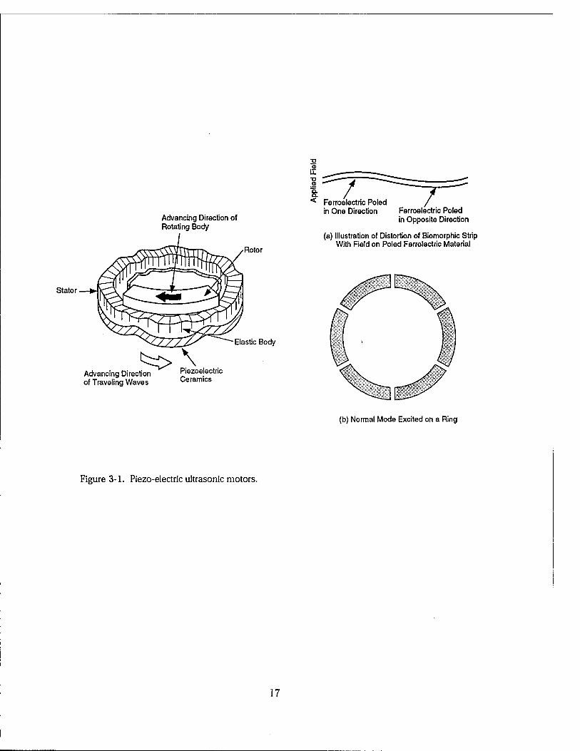
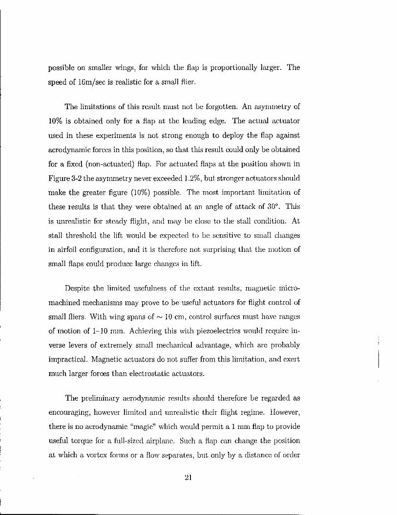
Piezo-electric ultrasonic motors represent a novel motor design in which
vibrational motion is transformed into rotational motion via a frictional cou
pling. The basic principle of an ultrasonic motor is illustrated in Figure
3-1. The source of the vibrations in the motor is a piezo-electric cylinder
to which segmented electrodes have been attached. By applying voltages of
alternating signs to the electrodes, a standing wave is induced in the cylin
der. The piezo-electric cylinder is tightly attached to an elastic material
which amplifies the displacements due to the standing wave. The rotor of
the piezo-electric motor is placed in frictional contact with the elastic ma
terial, and obtains a direct rotational motion as a result of the interaction
with the standing wave. Such motors have been developed and commer
cialized in Japan, and are used for automatic focusing in camera lenses.
16
Stator
Advancing Direction of Rotating Body
'''''''''''9 D'''''ti~ ':;""""0 of Traveling Waves Ceramics
Figure 3-1. Piezo-electric ultrasonic motors.
17
"C a; u: ] ~-~~--~~==~==~~ ]: Ferroelectric Poled I.
in One Direction Ferroelectnc Poled in Opposite Direction
(a) Illustration of Distortion of Biomorphic Strip With Field on Poled Ferrolectric Material
(b) Normal Mode Excited on a Ring
The miniaturization of piezoelectric motors is complicated by the diffi
culty of working with ceramic piezoelectrics. The possibility of circumventing
these difficulties has arisen due to recent materials development in the fabri
cation of thin film piezoelectric materials using sol-gel processing techniques.
This technology appears especially attractive as a method of incorporating
piezo ceramics directly onto a silicon substrate. Using these techniques, A.
Flynn at MIT, in collaboration with K.R. Udayakumar of Penn State, has
fabricated thin film motors as small as 0.3 JIm thick and 0.8 mm in diameter
and demonstrated the capability to rotate supported lenses at 100-300 rpm,
with an estimated torque of 41 pNm. (In contrast, Flynn has demonstrated
for a small (8 mm) bulk motor efficient operation with stall torque of ap
proximately 1 mNm.) The results on these thin film motors are a feasibility
demonstration only, which indicate the potential of micromotor development
in the context of a number of fabrication problems which must be solved to
make a wor&'1ble device. Continuing work on fabricating films that are free
of pinholes and in developing processing techniques such as laser etching to
form the stator appears promising.
3.2.2 Magnetic Actuators
Small remotely piloted vehicles have numerous battlefield applications,
chiefly in reconnaissance and sensor delivery. We discussed some of these
vehicles in JSR 93-150 "Fly on the Wall" , and were therefore pleased to learn
of Marvin Pope's work at Lincoln Laboratories on "Little Things", airplanes
small enough to fit in a hand. One of the problems of such very small
airplanes is their control systems. There is concern that it will be difficult
to miniaturize conventional model airplane actuators and control surfaces to
18
the required sizes. We have not investigated this, but instead describe an
application of MEMS technology which may provide an alternative solution.
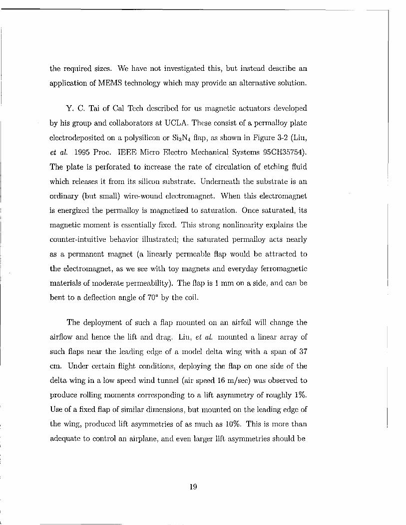
Y. C. Tai of Cal Tech described for us magnetic actuators developed
by his group and collaborators at UCLA. These consist of a permalloy plate
electrodeposited on a polysilicon or Si3N4 flap, as shown in Figure 3-2 (Liu,
et al. 1995 Proc. IEEE Micro Electro Mechanical Systems 95CH35754).
The plate is perforated to increase the rate of circulation of etching fluid
which releases it from its silicon substrate. Underneath the substrate is an
ordinary (but small) wire-wound electromagnet. When this electromagnet
is energized the permalloy is magnetized to saturation. Once saturated, its
magnetic moment is essentially fixed. This strong nonlinearity explains the
counter-intuitive behavior illustrated; the saturated permalloy acts nearly
as a permanent magnet (a linearly permeable flap would be attracted to
the electromagnet, as we see with toy magnets and everyday ferromagnetic
materials of moderate permeability). The flap is 1 mm on a side, and can be
bent to a deflection angle of 70° by the coil.
The deployment of such a flap mounted on an airfoil will change the
airflow and hence the lift and drag. Liu, et al. mounted a linear array of
such flaps near the leading edge of a model delta wing with a span of 37
cm. Under certain flight conditions, deploying the flap on one side of the
delta wing in a low speed wind tunnel (air speed 16 m/sec) was observed to
produce rolling moments corresponding to a lift asymmetry of roughly 1 %.
Use of a fixed flap of similar dimensions, but mounted on the leading edge of
the wing, produced lift asymmetries of as much as 10%. This is more than
adequate to control an airplane, and even larger lift asymmetries should be
19
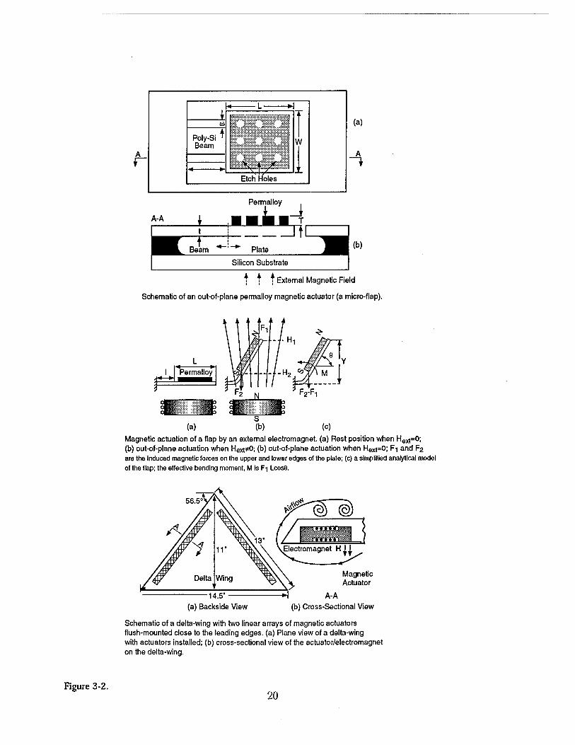
Figure 3-2.
I.. L ~I
(a)
A A r t
Permalloy
Plate (b)
Silicon Substrate
t t t External Magnetic Field
Schematic of an out-of·plane permalloy magnetic actuator (a micro-flap).
L
(a)
Magnetic actuation of a flap by an external electromagnet. (a) Rest position when Hext=O;
(b) out-of-plane actuation when Hext~; (b) out-of·plane actuation when Hext=o; Fl and F2 are the Induced magnellc forces on the upper and lower edges of the plale; (c) a slmplnied analytical model
of the flap; the effective bending moment, M Is F 1 Lcos8.
11·
Delta Wing
14.5· (a) Backside View
A-A
Magnetic Actuator
(b) Cross-Sectional View
Schematic of a delta-wing with two linear arrays of magnetic actuators flush-mounted close to the leading edges. (a) Plane view of a delta-wing with actuators installed; (b) cross-sectional view of the actuator/electromagnet on the delta-wing.
20
--- -- -- ----------------------------------
possible on smaller wings, for which the flap is proportionally larger. The
speed of 16m/sec is realistic for a small flier.
The limitations of this result must not be forgotten. An asymmetry of
10% is obtained only for a flap at the leading edge. The actual actuator
used in these experiments is not strong enough to deploy the flap against
aerodynamic forces in this position, so that this result could only be obtained
for a fixed (non-actuated) flap. For actuated flaps at the position shown in
Figure 3-2 the asymmetry never exceeded 1.2%, but stronger actuators should
make the greater figure (10%) possible. The most important limitation of
these results is that they were obtained at an angle of attack of 30°. This
is unrealistic for steady flight, and may be close to the stall condition. At
stall threshold the lift would be expected to be sensitive to small changes
in airfoil configuration, and it is therefore not surprising that the motion of
small flaps could produce large changes in lift.
Despite the limited usefulness of the extant results, magnetic micro
machined mechanisms may prove to be useful actuators for flight control of
small fliers. With wing spans of rv 10 cm, control surfaces must have ranges
of motion of 1-10 mm. Achieving this with piezoelectrics would require in
verse levers of extremely small mechanical advantage, which are probably
impractical. Magnetic actuators do not suffer from this limitation, and exert
much larger forces than electrostatic actuators.
The preliminary aerodynamic results should therefore be regarded as
encouraging, however limited and unrealistic their flight regime. However,
there is no aerodynamic "magic" which would permit a 1 mm flap to provide
useful torque for a full-sized airplane. Such a flap can change the position
at which a vortex forms or a flow separates, but only by a distance of order
21
its own size. Hence the lift asymmetry can only be of order the ratio of flap
size to wing chord, times a factor nominally of order unity but possibly an
order of magnitude larger under favorable (carefully chosen) conditions, as
in these experiments.
3.3 Independently Addressable Sensor Arrays
The Active Pixel Sensor, discussed in Subsection 2.2, can be considered
as the prototype for a new possibility that arises due to the shrinking size of
MEMS, that is the fabrication of arrays of independently addressable sensors.
Under conditions where a sensor is in a remote location, and communication
of output is stringently limited by power use, on-board processing and data
compression may become the keys to a usefully functional sensor.
3.3.1 Optical Imaging
In an imaging array of optical sensors, the possibility of independent
and parallel access to each pixel offers many new advantages. For example,
each pixel sensor can have its own "nano-processor" that communicates to
its nearest neighbors and a global command processor. The global processor
issues commands (in parallel) to each nanoprocessor. [This is similar to a
connection machine] The result is a specialized single instruction, multiple
data (SIMD) computer with a pixel sensor directly wired to each computing
element, detecting and processing images uncleI' program control, all on a
single chip. The nano-processors are extremely simple 'one-hit' processors
with a simple comparator connected to the optical sensor, so that analog to
22

digital conversion is accomplished in software.
Because all image detection, conversion and processing steps are ac
complished under program control, extremely flexible and powerful image
processing can be all accomplished on the sensor chip. Only the final desired
result needs to be transmitted off-chip. Thus besides the great reduction
in power consumption, size and weight over conventional systems, this ap
proach can greatly reduce the communication bandwidth needed to transmit
the information from the sensor.
A number of possible applications come to mind for such an 'intelligent
camera':
1. Images sometimes contain very bright objects such as the sun or flares,
when there are dim objects of interest in shadows, etc. (Remember
what happened to the Red Baron when he did not see his enemy at
tacking him 'out of the sun'.) Shutting down a single iris to compen
sate for the bright object, then causes the dim object to disappear. A
software program in our intelligent camera can discriminate and block
selectively, so that dim objects can be sensed and processed.
2. Often a camera will be set up to monitor a scene to detect some inter
esting activity. Our intelligent camera can be programmed for example
to provide only images of objects that move relative to the scene back
ground.
3. When communication is expensive, the intelligent camera can compress
the image according to the task of the camera and the activity in the
scene. For some tasks, the output might be only a bit, transmitted
when some object of interest is recognized by the intelligent camera.
23
4. The intelligent camera can also be programmed for image analysis, for
example to monitor environmental variables of interest. For example
it could report percent cloud cover.
5. The intelligent camera can also be programmed to provide autofocus,
camera positioning, zoom, external lightning and other robot operator
commands.
In summary, the intelligent camera can provide, powerful and flexible
image sensing, image processing, and data compression with large savings in
power consumption, weight, size and communication bandwidth.
3.3.2 Ultra Sound Imaging
A similar concept is likely to prove useful in ultrasound detectors as
discussed in JASON report JSR-95-145. There, even though pixel sizes are
larger, the possibility of handling the output of each pixel independently at
the sensor will allow significant advances in the number of pixels that can
be used in medical imagery, and in the types of imaging, such as confocal
imaging and holol:,'Taphy, that may be performed.
3.3.3 Mechanical Sensor Arrays
Independent addressability provides the potential for similar advanced
capabilities for arrays of mechanical sensors. One interesting example of such
an array is the recellt fabrication of cUI artificial cochlea by N. MacDouald's
24
group at Cornell. Using special processing techniques (not CMOS standard)
which involve fabrication in single-crystal Silicon, they can fabricate vertical
resonant bars which can be assembled into closely spaced arrays. To simulate
human hearing, they fabricated an array of beams of lengths ranging from
400 to 7000 /Lm, tailored to give a resonant frequency that varied exponen
tially along the array. To mimic the effect of the critical bands of frequency
response in hearing, different arrays were fabricated with gaps varying from
4 /Lm to 20 ILm to vary the coupling between the beams which arises from
the viscous medium (air) between them. In the first implementation, the
response of the beams was individually monitored via the Doppler shift of
a reflected laser beam. The development of on-board electronic monitoring
is underway via the incorporation of piezoelectric elements at the ends of
the resonators. The same 6'TOUp has also pioneered the incorporation of a
FET into the fabrication process In the fuure, this should allow front-end
electronics to be incorporated directly into the mechanical elements. Such a
capability opens the possibility of independently addressable arrays of me
chanical sensors with on board processing capabilities analogous to those
discussed for the active pixel array.
Similar resonator arrays, but at even higher frequencies, up to the Gi
gaHertz range, are a likely outcome of the work of M. R.oukes at Caltech.
Extremely small single resonators have been fabricated in single crystal sil
icon, using a variant of the process developed at Cornell. They achieve (in
vacuum) extremely high quality factors as well as high frequencies. The
incorporation of piezo-electric elements allows either frequency tuning or in
dividual sensing. Extension of these structures to arrays opens the possibility
of fabrication of single-chip high frequency spectrometers and filters.
25
3.4 High-Performance Accelerometers
The demands of high-performance in certain sensing applications such
as navigation and surveillance present serious challenges in devising micro
sensors. Here we discuss just one type of sensor, an accelerometer, and
note three different approaches to MEMS implementation of a device with
extremely high sensitivity. The theory of accelerometer design is well known:
an accelerometer consists of a proof mass suspended by a spring from an
external mounting, and a detection system to measure the displacement of the
mass in response to acceleration of the external mounting. In the case where
the frequency of the acceleration to be measured is substantially less than the
resonant frequency of the spring/mass system, the accelerometer response
(the displacement) to the input acceleration a in the frequency domain is
simply Zs(f) = a/w~, where the resonant frequency Wo = Jk/m and the
input acceleration is in meters per second squared per root Hertz. The signal
to-noise ratio at any frequency is 4//;$ w" which can become very poor
when the mass is small enough that Brownian motion is significant. Design
of a high-performance instrument requires an extremely sensitive method of
measuring the displacement, as well as optimizing the fundamental limits
of the signal to noise. Several different approaches to the design of high
performance accelerometers are underway.
The use of capacitive sensing of the gap spacing of the accelerometer
is being pursued by W. Kaiser of UCLA. In addition to the problem of vis
cous damping (see Subsection 2.1) which drives down the quality factor of
the spring system, and thus increases the noise, stray capacitances and ref
erence voltage stability also present serious practical problems in achieving
26
high performance. Kaser's group is addressing these problems by using bulk
micromachining steps to improve the mechanical performance, a suspended
measurement electrode to reduce p[trasitic capacitance, and a balanced ca
pacitance bridge measurement with the feedback to reduce problems of refer
ence stability. The bulk micro-machining requires a CMOS post-processing
step. Not all of these improvements have yet been incorporated in an op
timized accelerometer design. However, the first accelerometer designed us
ing this approach and a large proof mass (lOg) achieved a noise level of
10-9 9 / H zl/2, which is within the limits needed for a navigational accelerom
eter.
Another approach to position sensing is being explored by the gTOUp
of T. Kenny at Stanford. Here, the decreasing size of the accelerometer is
exploited to advantage by using electron tunneling as a displacement sensing
mechanism. Because the tunneling current varies exponentially as the sepa
ration, this approach has the immediate benefit of extremely high sensitivity.
However, l/f noise is a problem in tunneling, so that this technique encoun
ters noise limitations at low frequencies. Its first applications may therefore
occur in surveillance rather than in navigation. Early tests of accelerometers
based on this principle have yielded displacement response of 10-4 to 10-5
A/ Hz1/ 2 and noise levels of 2 x 10⁻⁷ 9 /HZ1/ 2 • This result was achieved under
relatively unfavorable conditions of a small proof mass (3 mg) and a low Q
suspension, suggesting that large improvements in performance are possible.
Finally, another highly sensitive displacement sensor has been developed
by the group of M. Roukes at Caltech. They have fabricated extremely small
vertical resonant beams with resonant frequency up to brigahertz. They are
able to sense displacements of these beams by applying externally a large
27
magnetic field and then monitoring the ac response of a current through a
closed circuit including the beam as part of the circuit path. Displacements
of the beam alter the area of the closed circuit, and in turn the inductive
response. In this way they are able to sense beam displacements with sen
sitivity as small as 10-4 A/Hzl/2, comparable to the sensitivity of a tunnel
sensor. Development of this technique for seismometry seems feasible.
The approaches being used to develop high performance accelerometers
will also be applicable to a wide variety of other types of sensors. Other
proposed applications include infrared detection, magnetometry, audio and
ultrasound detection.
28

4 BREAKTHROUGH TECHNOLOGIES
As the techniques of microfabrication are continually being improved
and pushed to smaller length scales, it becomes possible to address problems
of fundamental interest and potential application that were not earlier pos
sible. Extremely interesting work on the properties of ultra-small structures
is being performed by the group of Roukes at Caltech. By fabricating sin
gle crystalline structures of submicron length scale, they are able to address
a variety of fundamental problems. One problem is the effects on thermal
conductance when the phonon wavelength is comparable to the size of the
structure. Continuing fundamental work on such problems is likely to lead
to new technologies, such as long range potential applications in areas such
as radiation detectors and IR imaging arrays. Another problem addressable
with extremely small mechanical structures is the observation of quantum
mechanical behavior such as zero-point fiuctuations. Long-term potential
applications stemming from this research include the possibility of fabricat
ing a room-temperature single-electron transistor, which could effect a single
charge transfer by deflecting a small cantilever toward a counter-electrode.
Another area of potential applications, where many of the fundamental
issues have already been explored, is that of atom-by-atom lithography us
ing scanned probe manipulation or atom focusing. The potential of scanned
probe read/write devices capable of achieving information storage densities
limited by the size of the atom has been recognized almost since the first in
vention of STM. However, the practical limitation of the rate at which such
data storage might be possible has always been a stumbling block. Recent
advances in micro-motion and tip fabrication now offer at least the possibil-
29
ity that this difficulty could be overcome. An alternative technology which
has the advantage of being inherently parallel, is atomic lithography. Both of
these potential technologies have passed the stage of early feasibility demon
strations and need focused effort to determine whether, in fact, practical
technologies can be developed from them.
4.1 Scanned Probe Lithography
The two problems in scanned probe lithography are the development of
appropriate techniques for writing information, and addressing the problem
of doing such writing at useful rates. The possibility of writing has been
the subject of a wide range of studies with a large number of mechanisms
identified. The mechanisms most likely to result in a successful application
are those in which a resist is used in a manner analogous to electron beam
lithography. Standard e-beam resists have been evaluated for exposure using
field emitted electrons from a STM tip, indicating that the lower energy elec
trons used with the STM tip resulted in improved resolution due to reduced
electron scattering. Optimization of resists for STM or AFM exposure is
one major effort that will need to be undertaken to develop scanned probe
lithography. Two examples of resists that appear highly successful at expo
sure levels achievable with existing scanned probe techniques are the use of
hydrogenated amorphous silicon, and the use of spin-on-glass. In the former
case, an amorphous silicon layer is passivated with hydrogen, and then the
hydrogen is field-desorbed by passing an AFM tip, with an applied voltage
ranging from 4 to 25 V, over the surface. Simultaneous exposure to oxygen
causes the de-passivated region to become oxidized and resistant to subse
quent chemica~ or plasma etching. The oxide line widths drawn in this way
30
are as small as 2 nm wide, depending on the applied voltage and the speed
of the scan. Scan speeds on the order of 1p,m/s are used. The technique has
been used by two groups (at NRL and at Stanford) to fabricate FET struc
tures with critical sizes ranging from 30 nm to 0.1 p,m. Another resist that
has been demonstrated is spin-on-glass (siloxane), which can be deposited
and exposed with an AFM tip biased to 70 V and tip-sample currents of a
nA. It is believed that the exposure of the resist causes local decomposition
with the release of methyl groups forming regions with high organic content
that are resist to subsequent oxide etch. Write speeds greater than 1 mm/s
were demonstrated, with the ultimate rate limited by the response of the
scanner rather than the response of the resist.
Quantitative studies of resist sensitivity in both STM and AFM expo
sure mode will be needed to develop proximal probe lithography. In STM
mode, the typical tunneling current is a nano-amp. Once a sensitivity is
measured for a tunnel resist, it will be straightforward to apply the same
statistical analysis used in e-beam and im-beam lithography to determine
the maximum rate for a desired resolution. The same analysis for the AFM
mode, however, presents an interesting problem. The exposure mechanism
depends on the strength of the electric field rather than a (statistically vari
able) number of exposing particles. Determining exposure reliability in this
case will require some research to improve understanding of the exposure
mechanism.
While the development of appropriate resist technology will provide one
limit to achievable speeds of scanned probe lithography, another limit will be
the speed with which the probe tip can be scanned across the surface. To im
prove scan speeds, one can devise very rigid, high speed scanners, and one can
31
consider the use of multiple tips with integrated control electronics. Both of
these approaches appear feasible with fabrication techniques that are under
development, for instance in N. McDonald's group. The use of single crystal,
high-resonance-frequency beams in displacement actuators allows the forma
tion of high frequency (albeit small area) scanning drives. A demonstration
of a prototype micro-STM developed at Cornell shows that this approach can
be considered seriously. Drive actuators with resonance frequencies above a
megahertz have been demonstrated, suggesting a mechanical limitation on
write-rates of up to 105 lines/so So far scan areas are limited to a width of a
micron or less. To write to this area at 10 nm resolution would only require 1
ms, if only mechanical effects limited the rate. Given that both the speed up
control electronics and resist sensitivity will also playa role in determininig
the rate, this speed, which still corresponds to 105s per square centimeter,
would need to be improved for large volume applications. The incorporation
of multiple tips onto a scanner, or the use of multiple scanners each with a
single tip provide the most obvious methods of increasing write speeds and
areal coverage. There are serious engineering problems that would need to be
overcome to accomplish this. First, the tips would have to be independently
addressable both in terms of applied voltages to control the write pattern,
and in terms of height adjustment. Secondly, the relatively small area over
which the tip can be scanned compared to the area occupied by the drive
mechanism would require either precise stepping of the sample relative to
the scanner, or serious modification of the actuator design, or both. The
first problem harks back to issues of independently addressable sensor ar
rays, discussed in Section 2, and clearly can be addressed with developing
technology to incorporate electronics onto micro-mechanical structures. The
second problem is certainly addressable by extension of existing technology.
Rotating a sample under an AFM tip has been demonstrated as a write
32
mechanism at data rates of 100 kHz, and application of multiple AFM tips
has also been demonstrated, although without independent feedback on the
individual probes.
Whether all of these issues can be solved to result in a technology com
petitive or superior to electron or ion beam techniques as design scales shrink
into the 0.1 /-lm regime and below is open to question. However, the fun
damental understanding and demonstrations that are in place indicate that
there is at least a feasibility of a useful scanned probe lithographic technology.
A focused investment into the development of such a technology seems war
ranted. In addition to potential high-payoff in micro-electronics at shrinking
size scales, the technological development of independently addressable tip
arrays is likely to have impact in the area of flat panel displays, and in the
development of highly focused electron sources.
4.2 Atomic Lithography
By now, laser cooling, and even trapping, of matter is a well known
phenomenon. In the context of this study, there is already a possible appli
cation: high resolution lithography using cooled beams of atoms. There are
several versions of this possibility. In the simplest one, fine lines of metals
can be deposited on a wafer as follows: An electron beam is used to create
a high resolution mask. The mask is then placed upon (or very close to)
the surface of a wafer. A neutral beam of Al or other metal from a thermal
source then floods the mask/wafer, depositing conductor where there is no
mask. If there were no gap between the mask and the surface, the transverse
energy spread of the neutrals would not matter, i.e. there would be no need
33

to have a highly collimated atomic beam. However, as the wafer begins to
develop surface features of, for example, 1 micron in height, the transverse
velocity must be below 1/30 of the longitudinal velocity, if, for example 30
nanometer features are to be produced, requiring the neutral beam to have
0.1 % or less of its energy in the transverse direction. Gaps larger than 1
micron require even less transverse energy. This can be accomplished with
low energy neutral beams by laser-cooling the transverse beam motion. Fifty
nanometer feature sizes have been demonstrated with this technique using
a Na beam and a 50 mW dye laser (loa micron diameter). The neutrals
can do virtually no damage to the surface since they have less than 0.1 eV
longitudinal energy.
A more complicated possibility involves neutral He or Ar atoms in a
metastable excited state that are generated in a discharge. Because a laser
can be used to pump the neutrals out of the metastable state so that they
can undergo a transition to the ground state, the laser can bring about the
patterning of the neutral beam by its spatial intensity pattern. When the
resulting partly still excited and partly quenched neutral beam reaches a
specially prepared surface, the regions of the surface exposed to the portion
of the beam not de-excited by the laser is damaged and removed by the
residual excited state energy. Therefore, with enough neutral beam fiuence,
the layers(s) underneath the original surface layer can be uncovered and
then chemically etched, while the remainder of the underlying layer remains
protected.
Since neutral beams from thermal sources are not very intense, it takes
minutes to deliver the fiuence necessary to carry out a single production
step such as depositing interconnects (deposition of 100 A of Na takes 10
34
minutes). Therefore, it would seem most interesting to use laser-beam-cooled
neutral beams for special purpose lithography that is difficult to do by other
means. One such possibility is to cool and focus a uniform neutral beam by
the coherent electric field pattern in two crossed laser beams tuned so as to
enable stark shift focusing of the neutrals in the beam. A two-dimensional
array of focal points in a highly accurate periodic pattern of nanometer-scale
fiducial points can be produced at the focal plane. In two dimensions, one
half wavelength spacing has been achieved, and by clever use of a pair of
polarized lasers, a one-eight wavelength pattern of spots has been obtained
in one dimension. The focal length can be as short as tens of microns. In
order to achieve a one micron depth of field, however, a longer focal length
and a longitudinally (as well as transversely) cooled neutral beam would be
required.
Beyond this, the question arises as to whether aperiodic patterns can be
written on a resist (or equivalent surface layer) by laser-focusing of neutral
beams. The idea of using holographic lenses with crossed lasers to produce
arbitrary patterns in space to achieve this goal may be possible in principle.
However, this possibility is still being investigated theoretically, and its limi
tations (on resolution, requirements on the gratings, etc.) are not yet worked
out.
35
A APPENDIX: SMALL, CHEAP SENSORS (This Appendix is taken from JSR-95-125, "Microsurveillance of the Urban Battlefield" )
A.I General Considerations
Now that we have discussed data transport issues, it is time to discuss
the sensors that generate the data. We will focus on imaging sensors, not
because other types are uninteresting, but because the video sensor poses the
hardest design problem and generates the bulk of the data.
We need a miniaturised, low-power combineel sensor anel communica
tions packa,ge cheap enough to be treated as a throwaway item. The familiar
CCD detector technology appears to be incompatible with the requirements
of our problem for reasons of both cost and power consumption. However,
a new detector technology, called CMOS active pixel arrays, appears ideally
suited to our needs. The important facts about it are that: the pixel array
is created by standard CMOS manufacturing steps and can be integrated on
a single chip with processor and memory; individual pixels can be directly
addressed just like RAM memory locations; circuit elements can be colocated
with detector pixels to carry out operations, such as compression, directly.
The ability to put detector, processor and memory directly on a single CMOS
chip has obvious beneficial implications for size and cost. The details of this
technology and some other opportunities it presents are discussed in a com-
37
panion JASON report, entitled "Unconventional Integration" (JSR-95-120
and JSR-95-121).
The primary issues in designing a sensor package for this application are
size, cost and power consumption versus the bit rate needed to send useful
video imagery. As we will see in the next subsection, the active pixel array
technology seems to put all these parameters in an interesting range.
Although we have not had time to pursue the subject very far, it is clear
that unconventional methods of emplacing the sensor packages will be needed
(careful installation by trained technicians is obviously not a useful model).
We like the idea of "fire and forget" emplacement in which the package is fired
at, and sticks to, a convenient surface. The package, including the optics,
would need a certain level of shock hardness and some means of ensuring
that the emplaced sensor would have a useful field of view. Putting all the
electronics, detection and R.F elements 011 a single chip would confer a level of
mechanical robustness which should make such emplacement schemes easier
to develop.
A.2 Strawman Design of an Emplaced Video Sensor
To give a concrete sense of what can be done with the new sensor tech
nology, we present a strawman design of a sensor/communicator packc'1ge that
would, supposing the optics and emplacement issues can be solved, meet the
needs of our battlefield microsurveillance scheme. More details on the tech
nology issues involved can be found in the companion .JASON report entitled
"Unconventional Integratioll". A prilllary goal is to make the package as
38
small and light as possible. Given the communication needs, battery energy
density is the primary determinant of size and weight. Zinc-air batteries,
which store 20 Whr per cubic inch, are a very attractive choice: two cubic
inches of battery volume give a 400 hour active lifetime at 100 mW average
power consumption and correspondingly longer at lower power.
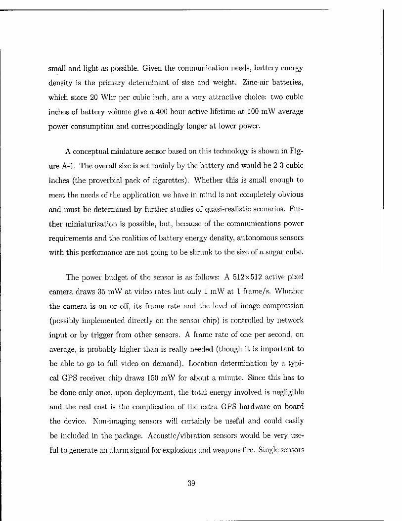
A conceptual miniature sensor based on this technology is shown in Fig
ure A-I. The overall size is set mainly by the battery and would be 2-3 cubic
inches (the proverbial pack of cigarettes). \Vhether this is small enough to
meet the needs of the application we have in mind is not completely obvious
and must be determined by further studies of quasi-realistic scenarios. Fur
ther miniaturization is possible, but, because of the communications power
requirements and the realities of battery energy density, autonomous sensors
with this performance are not going to he shrunk to the size of a sugar cube.
The power budget of the sensor is as follows: A 512x512 active pixel
camera draws 35 mW at video rates but only 1 mW at 1 frame/so Whether
the camera is on or off, its frame rate and the level of image compression
(possibly implemented directly on the sensor chip) is controlled by network
input or by trigger from other sensors. A frame rate of one per second, on
average, is probably higher than is really needed (though it is important to
be able to go to full video on demand). Location determination by a typi
cal GPS receiver chip draws 150 m W for about a minute. Since this has to
be done only once, upon deployment, the total energy involved is negligible
and the real cost is the complication of the extra GPS hardware on board
the device. Non-imaging sensors will certainly be useful and could easily
be included in the package. Acoustic/vibration sensors would be very use
ful to generate an alarm signal for explosions and weapons fire. Single sensors
39
Possible other sensors acoust i c/vi brat ion
.. betteries .. ~ Radio/GPS Interface
Optics Fish-eye lens or Possible zooml poi nt capabil i ty
with possible on-board image processing/data compression
Figure A-I. Strawman layout of a miniature imaging sensor.
40
would probably have a large false alarm rate (from vehicle backfires and the
like), but correlating the output of nearby sensors might turn this into a
useful tool. At a rough guess, such sensors would draw power at a rate of
l-lOmW. This would be a small component of the overall power budget.
The dominant component of the power budget is the RF power needed
to transmit the data. Just to recall, with conservative assumptions about
efficiencies and no antenna gain, the link powers needed for typical data
rates and link ranges are (at S-band): 2 mW for 106 bitsls at 100m, 20 mW
for 105 bits Is at 1000m, 200 mW for 104 bitsls at 10 km. Depending on
how the network is configured, the required communications power should
be somewhere from a few tens of m\,y to about 100 mW.
41

B APPENDIX: LOW-POWER A/D CONVERSION (This Appendix is taken from JSR-95-145, "Ultrasound")
B.1 Overview
We have already pointed out the importance of low-power analog-to
digital (A/D) conversion for large ultrasound arrays. This report analyzes
the power dissipation of a straightforward A/D converter.
B.2 Block Diagram
Figure B-1 shows a block diagram of a typical A/D converter. Each
sample interval an analog input signal is placed on the positive input of a
comparator. The "logic" and "D / A" Llocks then generates a series of voltages
to which the input is compared. The output is generated as a result of these
comparisons.
Different styles of A/D converters vary the sequence of voltages being
compared and the manner in which they are generated. Some popular styles
include:
1. Successive Approximation: The logic generates a series of voltages that
perform a binary search for the input voltage by repeatedly halving the
interval in which the voltage rnay be contained. This generates an b-bit
digital output in b steps with the output of the comparator containing
43
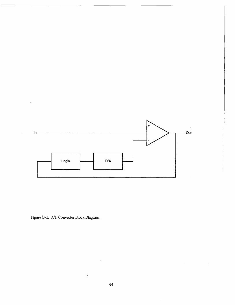
In ~ V
Out
Logic D/A t---
Figure B-l. AID Converter Block Diagram.
44
the bits of the output MSB-first. The binary search can be performed
serially in a single stage or as a pipeline of stages, one per bit.
2. Slope or Dual-Slope: The logic generates a "ramp" independent of the
comparator output and the point at which the comparator switches
indicates the input voltage. The ramp is usually generated by an ana
log integrator while the time interval is measured by sampling a free
running counter. This method requires 2/J steps to generate an b-bit
output.
3. Oversampled: The logic closes a loop that "delta-codes" the input.
That is the logic counts up when the output of the comparator is one
and down if it is zero. Some COllverters use delta-sigma rather than
straight delta coding. In either case an integrator can be used to gen
erate the voltages eliminating the need for a full D / A. The output
stream is decimated to produce an b-bit digital signal at 2-/J the orig
inal sample rate. These converters are popular in systems where the
oversampling and decimation obviate the need for analog anti-aliasing
filters with sharp cut-off's.
4. Flash: A flash converter performs all of the operations of a slope con
verter, but in parallel rather than serially. A resistive or capacitive
voltage divider generates 2/J equally-spaced voltages and 2/J compara
tors compare the input signal to all of these voltages simultaneously.
A log-depth logic circuit encodes the output of the comparators into
a b-bit signal. Flash converters are used in situations where very low
latency is required. For total throughput a successive approximation
converter is preferred as b successive approximation converters have the
same throughput as a single flash converter at b/2/J the cost.
45

5. Hybrid: A hybrid converter is a successive approximation converter
that uses an m-bit flash converter at each stage to perform a b-bit con
version in b 1m steps. Rather than using a D I A in a feedback loop, the
signal is usually recentered and rescaled between each step to perform
the 2m -ary divide and conquer search.
B.3 Power Calculation
Consider the problem of performing a b bit AID conversion with sample
rate f. If a successive approximation converter is used, the energy required
for the conversion is
where Ee is the energy required per comparison, ES1V is the switching energy
of the technology, 9 gates switch for the 10f,ric to prepare for each comparison,
and Esda is the DI A conversion energy. Each of these components of power
is dealt with in more detail below.
The slope-based and oversampling converters require considerably more
power than this because although they have simpler logic and D I A com
ponents this advantage is overwhelmed by the fact that they perform 2b
comparisons to convert a b-bit number rather than b.
B.3.! Comparator
The comparator can be realized as a clocked sense-amplifier, as a static
46
differential amplifier, or as an inverter with a switched capacitor input. In the
case of the static amplifier, the current bias is set so it has just enough output
current to swing its output capacitance in one bit time. A self-biasing circuit
can be used to adjust the current source to this minimum current value. The
output capacitance includes the self capacitance of the amplifier, a small
amount of wiring capacitance, plus a minimum-sized inverter to buffer the
signal for distribution to the logic. If transistor sizes are kept small a total
capacitance of 50 fF is reasonable in an 0.5 Itm process. Assuming half the
bias current goes into the output and a 3.3V supply voltage this gives a
comparison energy of
Ec = 5 x 10-14 (3.32)(2) ~ IpJ
With the clocked sense amplifier the clock load is increased by about lOfF to
drive isolation devices and to gate on the amplifier current source. Also the
regenerative feedback slightly increases the self-capacitance of the amplifier,
to about 70fF for typical device sizes. Thus a clocked sense-amp would
have a slightly higher comparison energy of about 1.6pJ but would have the
advantage of not requiring a speed-dependent bias current.
An inverter with a switched input capacitor would have a somewhat
larger power dissipation as it requires a DC current (when operated in the
middle of its range), current to charge its input capacitor, and clock power
to drive the switches.
B.3.2 D/A
The D/ A converter can be realized using switched capacitors, with an
R-2R ladder, or with a series of progressi vely-sized transistors. The R-2Ft ap-
47
proach will not be considered as precise-valued resistors are hard to fabricate
on an MOS integrated circuit.
The switched capacitor D I A takes advantage of the subdivision prop
erty of the voltage sequence in a successive approximation AID converter to
produce the required voltage sequence by charge sharing between two equally
sized capacitors. Initially one capacitor is charged high and the other low
to bound the interval. A capacitive voltage divider is then used to find the
midpoint of the interval. This midpoint voltage is then placed on one of the
two capacitors to define the next interval and the process is repeated.
This approach requires two vol tage followers that must have enough bias
current to copy voltages accurately in a bit time. With lOOfF capacitors, each
follower would consume about 2pJ per bit and another 2pJ would be used in
charging each capacitor for a total of 8pJ per bit.
The transistor approach, which to our knowledge is original, replaces the
negative input of the comparator with a parallel connection of NFETs with
progressively increasing sizes. Rather than being connected to an analog
voltage, the gates of these transistors are directly controlled by the logic.
They are sized so that the comparator will "trip" when the input voltage
exceeds the binary value encoded on the transistor gates. The sizes are not
simply powers of two, but rather must match the quadratic I-V characteristic
of the MOSFET.
The only power consumed by this approach is caused by the increased
capacitive load on the output of the logic which switches at most once per
cycle. For small b, this load is small but for large b it increases exponentially.
48
A rough expression for the energy required per bit is:
For an 8-bit signal, this is just O.2pJ per bit.
Alternatively power-of-two sized transistors can be connected to a polysil
icon load resistor to generate a voltage that is a linear function of the binary
input. This will roughly double the comparison energy.
In either case, capacitance is minimized by using a minimum sized device
in the middle of the size range and using devices with minimum Land W > L
in the upper half of the range and minimum vV and L > W in the lower half
of the range.
B.3.3 Logic
The logic required for a serial successive-approximation converter is a
register to hold each bit of the current digital value, and ring-counter shift
register to select the next bit to update, and a MUX to select the input to
each bit of the register. Each register bit toggles exactly once per cOllversion
cycle as does each ring counter bit. If we count switching each re6rister as
four switching events and add two switching events for the associated MUX,
the constant 9 is 10 switching events per bit. With an Esw of O.lpJ this gives
a logic energy of IpJ per bit. For a pipelined converter the ring counter and
multiplexer are not required reducing this power slightly.
49

B.3.4 Example
For example a b = 8-bit converter with a transistor D / A operating at 1
MHz would have a total power dissipation of
PSCL = 8 x 10⁶(lpJ + 0.2pJ + 1pJ) ~ 20jJW .
Even if we increase this by a factor of 5 to use the 1.6pJ sense amp, the 8pJ
capacitive D/A and to account for overhead the power is still only 100p,W.
B.4 Other Issues
B.4.! Resolution and Linearity
To operate at very low power, one uses minimum sized devices. These
devices can have relatively large parameter mismatch (on the order of 10%)
which limits the linearity of the converter. It is more power efficient to correct
these linearities digitally via a PROM than it is to increase the component
size to eliminate them.
To get adequate resolution in the presence of mismatches, capacitor
leakage, and other eHects, the converter may have to produce more bits
of intermediate result than are required in the final linearized result. The
converter must resolve voltage steps that are no more than one LSB apart.
Usually adding one additional bit is sufficient to provide this spacing.
50

B.4.2 Low-Voltage Operation
The analysis above has not considered the possibility of voltage scaling.
If the circuit is operated slowly, the supply voltage can be reduced which
reduces power quadratically. While very slow circuits can be operated in the
subthreshold region, most practical circuits are limited to supply voltages of
about IV to remain comfortably above the device threshold. At IV power
is reduced by a factor of 9 over the numbers calculated above. Low voltage
operation does require that the input voltage be scaled to the small power
supply.
51
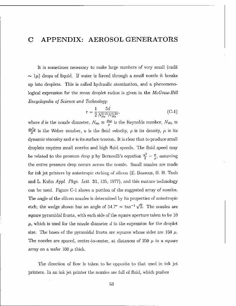
C APPENDIX: AEROSOL GENERATORS
It is sometimes necessary to make large numbers of very small (radii
'" IlL) drops of liquid. If water is forced through a small nozzle it breaks
up into droplets. This is called hydraulic atomization, and a phenomeno
logical expression for the mean droplet radius is given in the McGraw-Hill
Encyclopedia of Science and Technology:
1 5el r = ? NO.15 N O.20 ' (C-1)
~ He We
where d is the nozzle diameter, NHe - ~ is the R.eynolds number, Nwe = d1:P is the Weber number, 'lL is the fluid velocity, p is its density, It is its
dynamic viscosity and a is its surface tension. It is clear that to produce small
droplets requires small nozzles and high fluid speeds. The fluid speed may
be related to the pressure drop p by Bernoulli's equation 1;2 = ~, assuming
the entire pressure drop occurs across the nozzle. Small nozzles are made
for ink jet printers by anisotropic etching of silicon (E. Bassous, H. H. Taub
and L. Kuhn Appl. Pltys. Lett. 31, 13S, 1977), and this mature technology
can be used. Figure C-I shows a portion of the suggested array of nozzles.
The angle of the silicon nozzles is determined Ly its properties of anisotropic
etch; the wedge shown has an angle of 54.7° = tan- l J2. The nozzles are
square pyramidal frusta, with each side of the square aperture taken to be 10
IL, which is used for the nozzle diameter d in the expression for the droplet
size. The bases of the pyramidal frusta are squares whose sides are 150 Il.
The nozzles are spaced, center-to-center, at distances of 250 Jt in a square
array on a wafer 100 Jt thick.
The direction of flow is taken to Le opposite to that used ill ink jet
printers. In an ink jet printer the nozzles are full of fluid, which pushes
S3
~--+-25011
V Holes in Steel Plate Bases of Nozzle Pyramid
25011
(b) Plan
Fe Fe Fe Fe
Si Si Si Si
100 plane
25011----tl~~1
(a) Cross -section t Fluid Flow
Figure Col. Nozzle design, including supporting steel, etched onistropically in 100 Si water, 100J.l thick. Nozzles are on 250J.l centers.
54
,---------------------------------------
outward on the walls of the nozzle. The stress is largely tensile, and
its concentration at these sharp edges would threaten the brittle silicon with
catastrophic failure. This is not a danger in the printer, in which the ink is at
low pressure, but would be a serious problem at the high pressures required
in the atomizer. With the indicated direction of flow the nozzles contain only
air at atmospheric pressure and tiny droplets of liquid which do not contact
its walls, so there is no tensile stress to concentrate. We assume p = 100 bars
= 1500 psi, within the range of hydraulic technology (pressures up to 5000
psi are used). Then Bernoulli's equation implies a fluid discharge velocity
u = 1.4 X 10⁴ em/sec, NRe = 1400 and NWe = 3000. The mean drop radius is
then r' ~ 1.7 ft. The total mass of solution required to make 1017 drops is 2
tons, which can be carried on an aircraft of moderate size, or atomized on the
ground. Smaller nozzles would produce smaller droplets, with T ex: dO.(;5. The
total mass flow rate through the nozzle is proportional to its area d2, and the
mass of each droplet is ex: T3 ex: dl.!l5. Hence the number of droplets produced
per unit time, which is the important parameter, is essentially independent
of the nozzle dimensions and is
IV ~ 7 X 10⁸ ]J sec-I. ( )
1.33
1500psi (C-2)
Nozzles even smaller than 10 It are therefore desirable, if they can be made,
because they consume less fluid. We assume d = lOlL only because it ap
pears to be readily manufacturable with standard silicon technology, without
extraordinary control on the wafer thickness and uniformity of the etch rate.
Fluid flows through each nozzle at a rate 'lUP = 1.4 X 10⁻² cm3/sec, or
50 cm3/hr. In order to atomize the entire 2 tons of solution (into 10 17 drops)
in an hour would require 40,000 nozzles. The hydraulic power required is
about 6 k W, which is feasible. The nozzle array lllay be fabricated from a
single silicon wafer at 250 JL spacing in an array 5 crn square. However, such
55
a single large array would be vulnerable to breaka,ge. We therefore consider
100 separate silicon chips, each containing 400 nozzles filling an area of 0.25
cm2 • Each chip would be circular, with diameter of about 6 mm, and each
would be mounted at the end of a pipe containing the pressurized solution.
The silicon chips separate a region of pressurized liquid at 1500 psi from air at
atmospheric pressure. A chip 100 JL thick and 6 mm in diameter cannot hold
such a pressure drop. A thicker slab of silicon would be stiffer, but because
the angle of anisotropic etch is fixed the width of the bases of the nozzles
increases in proportion to the slab's thickness, as does their spacing. The
diameter of a chip containing a given number of nozzles must therefore also
increase in proportion to its thickness. The peak stress is then independent
of thickness and depends only on (and is proportional to) the number of
individual nozzles. Silicon can tolerate a tensile stress of roughly 15,000 psi,
so that if silicon alone is used each chip could contain only a few nozzles, and
many thousand chips would be required, each with its own plumbing.
We suggest instead that the silicon chips be backed with a perforated
steel plate, as shown in Figure C-1. The steel would contain holes 150 JL (6
mils) in diameter aligned with the nozzles in the silicon. Holes of this size
can be drilled by electric discharge machining. A single 400 wire tool could
drill the required steel plate in a single operation. The required thickness of
a uniform plate is determined by the maximum tolerable stress 8m (Standard
Handbook for Mechanical Engineers) as
_ (kp1.2) 1/2 h- -5' ,
1ft
(C-3)
where the constant k is 1.24 for simply supported edges and 0.75 for fixed
edges. The perforated plate we discuss has 30% of its volume drilled out,
whose effect we approximate by dividing these values of x: by 0.7. Adopting
8m = 3 Kbar as a safe stress for steel and k = 1.8 for simply supporteel edges
56
yields h = 0.24r, or h = 0.72 mm for a 6 mm diameter disc. This is a modest
thickness, and implies holes only five times as long as their diameters, so
that few droplets should be lost by contacting the sides of the holes. For
comparison, the stress in a silicon chip unsupported by steel would be over
100 Kbar, far above its strength. Some droplets will inevitably strike the
sides of the holes in the steel, raising the concern that if enough solution
sticks to them the holes will fill with liquid and clog. It is uncertain that
this is actually a danger, because high velocity impact will tend to splash
wetting fluid off the surface and out the open end of the hole. Applying
a hydrophobic film to the steel would also reduce the danger of clogging;
small holes in a hydrophobic lllaterial are difficult to wet, even without the
cleansing action of the stream of droplets.
The silicon is pressed against the steel plate by the pressure of the
fluid. With negligible stiffness of its own because of its thinness, it acts as
a compliant membrane, and assumes the shape of the steel. The Young's
modulii of steel (1.9-2.1 MbaI') and silicon (1.9 MbaI') are very similar, so
the stress, as well as the strain, in the silicon are nearly the same as in the
steel against which it is pressed. The maximum tolerable tensile stress for
silicon is about 1 Kbar. Here the tolerable mean tensile stress may be much
less because of stress concentration at the edges of the pyramidal nozzles.
However, because the silicon is on the concave side of the bent steel plate
(concavity across the plate is assured by the use of simply supported edges) it
is everywhere in compression; brittle substances are generally able to tolerate
compressive loads substantially in excess to their strength in tension. If, even
so, the stress on the silicon is too high it may be reduced by thickening the
steel plate or by adding stiffening ribs to it; for example, increasing h to 1.25
mm reduces all stresses below 1 Kbar.
57
References
[1] Analog Devices, Monolothic Accelerometer ADXL50 Data Sheet T. B.
Gabrielson, "Mechanical-Thermal Noise in Micromachined Acoustic and
Vibration Sensors", IEEE Transactions on Electron. Devices, 40, 903,
1993.
[2] C. Mead, "A sensitive electronic photoreceptor," 1985 Chapel Hill Con
ference on VLSI, pp. 463-471, 1985.
[3] E.R. Fossum, "Ultra-low power imaging systems using CMOS image
sensor Technology," Proceedings of the SPIE, vol 2267, Advanced Mi
crodevices and Space Science Sensors (1994).
[4] A. Flynn, "Piezoelectric Ultrasonic Micromotors", Doctoral Disserta
tion, MIT, 1995.
[5] A. M. Flynn, et a1. "Piezo-electric Micromotors for Microrobots," J.
Micro electromechanical Systems 1, 44 (1992).
[6] K.R. Udayakumar, et al., "Ferroelectric Thin Film Ultrasonic Micromo
tors," Ferroelectrics, 160, 347, 1995.
[7] D. Haronian and N.C. MacDonald, "A Microelectromechanics Based
Artificial Cochlea", to be published, 1995.
[8] J. J. Yao, S. Arney, and N. MacDonald, "A fully suspended, movable,
single-crystal silicon, deep submicron MOSFET for nanoelectromechan
ical applications," Sensors and Actuators A40, 77, 1994.
[9] W.J. Kaiser, "New high-sensitivity microaccelerometer technology for
vibration control," preprint, 1995.
59
[10] T.W. Kenny, et al. "Wide-Bandwidth Electromechanical Actuators for
Thnneling Displacement Transducers," J. Microelectromechanical Sys
tems 3, 9, 1994.
[11] E.A. Dobisz and C.R. K. MarTian, "Scanning tunneling microscope
lithography: A solution to electron scattering," J. Vac. Sci. Technol.
B9, 3024 1991
[12] P.M. Campbell, E.S. Snow and P.J. McMarr, "Fabrication of nanometer
scale side-gated silicon field effect transistors with an atomic force mi
croscope," Appl. Phys. Lett. 66, 1388 1995.
[13] S.C. Minne, H.T. SOh, Ph. Flueckiger, and C.F. Quate, "Fabrication
of 0.1 /-Lm metal oxide semiconductor field effect transistors with the
atomic force microscope," Appl. Phys. Lett. 66, 703, 1995.
[14] H. Ryssel, et. "Ion Beam Exposure of Resists," Appl Phys A 27, 239
(1982).
[15] S.W. Park, H.T. Soh, C.F. Quate, and S.-I. Park, "Nanometer Scale
LithogTaphy at High Scanning Speeds with the Atomic Force Microscope
Using Spin-On.:.Glass," submitted to Appl. Phys. Lett., May 1995.
[16] J.J. Mamin and D. Rugal', "Thermomechanical writing with an atomic
force microscope tip," Appl. Phys. Lett. 61, 1003, 1992.
[17] Y. Xu, S. Miller, and N.C. MacDonald, "Microelectromechanical Scan
ning 'nmneling Microscope," to be published, 1995.
[18] S.C. Minne, Ph. Flueckiger, H.T. Soh, and C.F. Quate, "Atomic force
microscope lithography using amorphous silicon as a resist and advances
in parallel operation," J. Vac. Sci. Technol B13, 1380, 1995.
60

[19] M. Prentiss, G. Timp and N. Bigelow, "Using light as a stencil", Appl
Phys Lett., Vol 60, 1027 (1992).
[20] R. Gupta, J. J. McClelland and R. .1. Celotta, "Nanofabrication of a two
dimensional array using laser-focused atomic deposition", Appl. Phys.
Lett., Vol 67, 1278 (1995).
61

DISTRIBUTION LIST
Director of Space and SDI Programs SAF/AQSC 1060 Air Force Pentagon Washington, DC 20330-1060
CMDR & Program Executive Officer US Army/CSSD-ZA Strategic Defense Command POBox 15280 Arlington, VA 22215-0150
A R P A Library 3701 North Fairfax Drive Arlington, VA 22209-2308
Dr Arthur E Bisson Director Technology Directorate Office of Naval Research Room 407 800 N. Quincy Street Arlington, VA 20350-1000
Dr Albert Brandenstein Chief Scientist Office of Nat'l Drug Control Policy Executive Office of the President Washington, DC 20500
Mr. Edward Brown Assistant Director ARPA/SISTO 3701 North Fairfax Drive Arlington, VA 22203
Dr H Lee Buchanan, I I I Director ARPA/DSO 3701 North Fairfax Drive Arlington, VA 22203-1714
63
Dr Ashton B Carter Nuclear Security & Counter Proliferation Office of the Secretary of Defense The Pentagon, Room 4E821 Washington, DC 20301-2600
Dr Collier Chief Scientist US Army Strategic Defense Command PO Box 15280 Arlington, VA 22215-0280
Dr Ken Cress Office of Research and Development Washington, DC 20505
DTIC [2] Cameron Station Alexandria, VA 22314
Dr William Dally University of North Carolina Department of Computer Science Sitters on Hall, Campus Box 3175 Chapel Hill, NC 27599
Mr John Darrah Senior Scientist and Technical Advisor HQAF SPACOM/CN Peterson AFB, CO 80914-5001
Dr Victor Demarines, Jr. President and Chief Exec Officer The MITRE Corporation 202 Burlington Road A210 Bedfored, MA 01730-1420
Dr Alvin Despain 3273 Corinth Avenue Los Angeles, CA 90066
Dr Douglas Eardley 618 Miramonte Drive Santa Barbara, CA 93109
DISTRIBUTION LIST
Mr Dan Flynn [5] OSWR Washington, DC 20505
Dr Paris Genalis Deputy Director OUSD(A&T)/S&TS/NW The Pentagon, Room 3D1048 Washington, DC 20301
Dr Lawrence K. Gershwin NIC/NIO /S&T 7E47,OHB Washington, DC 20505
Dr David Hammer 109 Orchard Place Ithaca, NY 14850
Mr. Thomas H Handel Office of Naval Intelligence The Pentagon, Room 5D660 Washington, DC 20350-2000
Dr Robert G Henderson Director JASON Program Office The MITRE Corporation 7525 Colshire Drive Mailstop Z561 McLean, VA 22102
Dr Paul Horowitz Harvard University Lyman Laboratory of Physics Cambridge, MA 02138
Dr William E Howard I I I [2] Director of Advanced Concepts & Systems Design The Pentagon Room 3E480 Washington, DC 20301-0103
64
Dr Gerald J Iafrate U S Army Research Office PO Box 12211 4330 South Miami Boulevard Research Triangle NC 27709-2211
J A SON Library [5] The MITRE Corporation Mail Stop W002 7525 Colshire Drive McLean, VA 22102
Dr Anita Jones Department of Defense DOD,DDR&E The Pentagon, Room 3E1014 Washington, DC 20301
Mr. O' Dean P. Judd Los Alamos National Laboratory Mailstop F650 Los Alamos, NM 87545
Dr Bobby R Junker Office of Naval Research Code 111 800 North Quincy Street Arlington, VA 22217
Dr Jonathan Katz Washington University Department of Physics St Louis, MO 6333130
Lt Gen, Howard W. Leaf, (Retired) Director, Test and Evaluation HQUSAF/TE 1650 Air Force Pentagon Washington, DC 20330-1650
Dr Nathan Lewis California Institute of Technology Division of Chemistry and Chemical Engineering: 127-72 Pasadena, CA 91125

DISTRIBUTION LIST
Mr. Larry Lynn Director ARPA/DIRO 3701 North Fairfax Drive Arlington, VA 22203-1714
Dr. John Lyons Director of Corporate Laboratory US Army Laboratory Command 2800 Powder Mill Road Adelphi,MD 20783-1145
Col Ed Mahen ARPA/DIRO 3701 North Fairfax Drive Arlington, VA 22203-1714
Dr. Arthur Manfredi OSWR Washington, DC 20505
Mr James J Mattice Deputy Asst Secretary (Research & Engineering) SAF/AQ Pentagon, Room 4D-977 Washington, DC 20330-1000
Dr George Mayer Office of Director of Defense Reserach and Engineering Pentagon, Room 3D375 Washington, DC 20301-3030
Dr Bill Murphy ORD Washington, DC 20505
Mr Ronald Murphy ARPA/ASTO 3701 North Fairfax Drive Arlington, VA 22203-1714
65
Dr Julian C NaIl Institute for Defense Analyses 1801 North Beauregard Street Alexandria, VA 22311
Dr. Wolfgang K. Panofsky Stanford Linear Accelerator Center Stanford University P. O. Box 4349 Stanford, CA 94039
Dr Ari Patrinos Director Environmental Sciences Division ER74/GTN US Department of Energy Washington, DC 20585
Dr Bruce Pierce USD(A)D S The Pentagon, Room 3D136 Washington, DC 20301-3090
Mr John Rausch [2] Division Head 06 Department NA VOPINTCEN 4301 Suitland Road Washington, DC 20390
Records Resource The MITRE Corporation Mailstop W115 7525 Colshire Drive McLean, VA 22102
Dr Victor H Reis US Department of Energy DP-1, Room 4A019 1000 Independence Ave, SW Washington, DC 20585
Dr Fred E Saalfeld Director Office of Naval Research 800 North Quincy Street Arlington, VA 22217-5000
DISTRIBUTION LIST
Dr Dan Schuresko O/DDS&T Washington, DC 20505
Dr John Schuster Technical Director of Submarine and SSBN Security Program
Department of the Navy OP-02T The Pentagon Room 4D534 Washington, DC 20350-2000
Dr Michael A Stroscio US Army Research Office P. O. Box 12211 Research Triangle NC 27709-2211
Dr Jeremiah Sullivan 604 Burkwood Ct. E. Urbana, IL 61801
Superintendent Code 1424 Attn Documents Librarian Naval Postgraduate School Monterey, CA 93943
Ambassador James Sweeney Chief Science Advisor USACDA 320 21st Street NW Washington, DC 20451
Dr George W Ullrich [3] Deputy Director Defense Nuclear Agency 6801 Telegraph Road Alexandria, VA 22310
Dr Walter N Warnick [25] Deputy Director Office of Planning &Analysis, ER-5.1 Office of Energy Research U S Department of Energy Germantown,MD 2074
66
Dr Robert Westervelt Harvard University Division of Applied Sciences Cambridge, MA02138
Dr Edward C Whitman Dep Assistant Secretary of the Navy C3I Electronic Warfare & Space Department of the Navy The Pentagon 40745 Washington, DC 20350-5000
Capt H. A. Williams, USN Director Undersea Warfare Space
& Naval Warfare Sys Cmd PD80 2451 Crystal Drive Arlington, VA 22245-5200