Embed Size (px)
Citation preview
UNCLASSIFIED
A 296367
ARMED SERVICES TECHNICAL INFORMATION AGENCYARLINGTON HALL STATIONARLINGTON 12, VIRGINIAw
UNCLASSIFIED

NOTICE: When government or other drawings, speci-fications or other data are used for any purposeother than in connection with a definitely relatedgovernment procurement operation, the U. S.Government thereby incurs no responsibility, nor anyobligation whatsoever; and the fact that the Govern-ment may have foruulated, furnished, or in any waysupplied the said drawings, specifications, or otherdata is not to be regarded by implication or other-wise as in any manner licensing the holder or anyother person or corporation, or conveying any rightsor permission to manufacture, use or sell anypatented invention that may in any way be relatedthereto.

CONTRACT NO. AF33(657)8490BPS NUMBER 2)63-699.750F.817301-16)TASK NO. 817301-16
A APPLIED RESEARCH PROGRAM ONHIGH-TEMPERATURE RADIATION-RESISTANT
SOLAR-CELL ARRAY
QUARTERLY TECHNICAL PROGRESS REPORT NO. 3NOVEMBER 1962 - JANUARY 1963
Prepared for the
U.S. AIR FORCEmAERONAUTICAL SYSTEMS DIVISION
S WRIGHT-PATTERSON AFB, OHIO
C*4 By theTIA
ASTRO-ELECTRONICS DIVISION
DEFENSE ELECTRONIC PRODUCTS
RADIO CORPORATION OF AMERICA
PRINCETON, NEW JERSEY 19A
AED 1816 Issued: January 31, 1963
The work covered by this report was accomplishedunder Air Force Contract No. AF33(657)-8490, butthis report is being published and distributed priorto Air Force Review. The publication of this re-port, therefore, does not constitute approval by theAir Force of the findings or conclusions containedherein. It is published for the exchange and stimu-lation of ideas.

TABLE OF CONTENTS
Section Page
I SUMMARY OF WORK ACCOMPLISHED 1
A. GALLIUM ARSENIDE CELL DEVELOPMENT ANDFABRICATION 1
1. Cell Production 12. Cell Measurements (Electrical) 13. Efficiency versus Temperature 74. Shelf Life of Cells at 200 C 75. Silicon Monoxide Anti-Reflection Coating 86. References 9
B. ARRAY DESIGN AND TESTING 10
1. Summary 102. Array Construction 113. Investigation of Failures During Thermal-Vacuum Testing 11
a. Tests to Determine Cause of Failure 11(1) Quick-Cycle Test 11(2) Thermal-Vacuum Test of Unmounted Cells 12(3) Tests of RTV-60 Silicone Rubber Characteristics 12(4) Thermal-Shock Test of Cells at SMD-Somerville 14(5) Cell Measurements 14(6) Exposure of Cells with RTV-60 to Low Temperatures 15(7) Thermal-Vacuum Cycling Tests of GaAs-Cell Panel 15(8) Conclusions 23
4. Adhesive Work 255. Soldering Techniques 26
C. RADIATION TESTING 30
1. Electron Irradiation 30a. Introduction 30b. Description of the Cells 31c. Results of the 0. 8-Mev Run 31d. Results of the 5.6-Mev Run 37
ii
TABLE OF CONTENTS (Continued)
Section Page
e. Discussion of Results and Conclusions 39f. References 41
2. 1. 8-Mev Proton Irradiation 41
D. THIN-FILM GALLIUM ARSENIDE INVESTIGATION 43
1. Introduction 432. Methods of Producing GaAs Films 433. Discussion of Results 444. References 48
I1 WORK TO BE ACCOMPLISHED NEXT QUARTER 49
A. GALLIUM ARSENIDE CELL DEVELOPMENT ANDFABRICATION 49
B. ARRAY DESIGN AND TESTING 49
C. RADIATION TESTING 49
D. THIN-FILM GALLIUM ARSENIDE INVESTIGATION 49
iii

LIST OF ILLUSTRATIONS
Figure Page
1 Third-Quarter Pilot Line Production 2
2 First-Quarter Pilot Line Production 2
3 Second-Quarter Pilot Line Production 2
4 Total Pilot Line Production 3
5 Plot of Ln I versus m 6scm
6 Calculated Response of GaAs Solar-Cell Panel 17
7 Low Limit Protection Circuit 18
8 High Limit Protection Circuit 19
9 Actual Response of GaAs Solar-Cell Panel 20
10 Calculated Temperature Response of 0.2-Lb. Panel 21
11 Shape Factor (0Be) versus Angle Between Normal to Plate and
Earth Radius (0) 24
12 Circuit for Use of Silicon Wafer as Temperature-Measuring
Device; Schematic Diagram 25
13 Soldering Degradation (Short-Circuit Current) 27
14 Soldering Degradation (Open-Circuit Voltage) 28
15 Soldering Degradation (Voltage Change at 20 ma.) 29
16 Comparison of Relative Power Output and 0 for Cell No. MT-J4 34
17. Comparison of Relative Power Output and 0 for Cell No. S14HC 34
iv

LIST OF ILLUSTRATIONS (Continued)
Figure Page
18 Comparison of Power Output and Flux for GaAs and Si Cells 35
19 Comparison of Power Output and Flux for GaAs and Si Cells 37
20 Plot of P versus Flux for GaAs Cells (1. 8-Mev Protonmax
Irradiation) 42
21 Schematic Drawing of Apparatus for Forming GaAs Films on
Germanium Using GaAs as the Source Material 44
22 Schematic Drawing of Apparatus for Forming GaAs Films on
Germanium Using the Elements (Ga and As) as Component Raw
Materials 4512
23 Plot of (C) versus Voltage for Ag-GaAs Contact 47
24 I-V Characteristic of Cr-GaAs Contact, Forward Bias 48
v

LIST OF TABLES
Table No. Page
I Gallium Arsenide Cell Test Results 7
II Tension Test for Transmissibility of Loads by RTV-60 13
I Operating Conditions of Electron Irradiation 30
IV Initial Properties of Solar Cells 32
V Critical Flux of GaAs and Si Cells 33
VI Ratio of Final to Initial Values Based on Sunlight Measurements 36
VII * for 5.6-Mev Run 38c
VIII Changes Due to Total Bombardment, Based on SunlightMeasurements 38
IX Results of 1. 8-Mev Proton Irradiation 42
vi

APPLIED RESEARCH PROGRAM ON HIGH-TEMPERATURE
RADIATION-RESISTANT SOLAR-CELL ARRAY
QUARTERLY TECHNICAL PROGRESS REPORT NO. 3
NOVEMBER 1962 - JANUARY 1963
I. SUMMARY OF WORK ACCOMPLISHED
A. Gallium Arsenide Cell Development and Fabrication
1. Cell Production
During the third quarter, a total of 326 gallium arsenide cells werefabricated to meet the needs of the various temperature, radiation, and array designtests. A graph of frequency distribution versus cell efficiency for the third quarteris shown in Figure 1. A significant point is that during this period, the pilot line pro-duction peaked at a cell efficiency of about 8 percent. When this is compared withthe peaks of the distributions for the first and second quarters production shown inFigures 2 and 3, it can be seen that a progressive improvement in the typical cell ef-ficiency has been accomplished. Between the first and third quarters, the shift ofthe peak efficiency from 7 percent to 8 percent amounts to a net improvement of morethan 14 percent. The factors contributing to this advancement are improvementsmade in every step of the process including operator supervision.
Figure 4 shows a graph of frequency distribution versus cell efficiency for the totalpilot line production through the third quarter.
2. Cell Measurements (Electrical)
A solar cell is generally characterized electrically by the conversionefficiency, which is defined as the ratio of the maximum available power to the totalradiant power incident on the active area. The conversion efficiency is determinedfrom the current-voltage curve recorded under a tungsten light source whose intensityis adjusted to produce a specified short-circuit current on a "standard solar cell."
The specified short-circuit current of the standard solar cells is determined from sun-light measurements of short-circuit current, during which the total solar radiation is
measured using an Eppley Normal Incidence Pyrheliometer. These measurements

$Z4
z
mw
z
2
0
in0
In
iV
0 In In 0 I 0 In 0 In 0 In 0 I n 0 Io CD 0 0 v-t. I D ~ I ' " ~ ~S1133 JO V39mN
2

200
190
170
40
130
120
-j 110w
o 100wIw
TO
60
50
40
30
20
10
65 125 204 127 550 1 I i +
1 1.5 2.5 3.5 4.5 5.5 6.5 7.5 8.5 9.5CONVERSION EFFICIENCY (,q) PERCENT
Figure 4. Total Pilot Line Production
3
are made only on clear, bright days in the absence of haze and visible clouds. If
these conditions prevail, and the measured solar irradiation is greater than 90 milli-
watts per square centimeter, the measured short circuit current is extrapolatedlinearly to 100 milliwatts per square centimeter. This level of solar radiation was
selected for in-process testing because it is approximately the value reported byMoon (see Reference 1) for the maximum sunlight reaching the earth's surface, andbecause it is a value used by many researchers.
As previously indicated in Quarterly Technical Progress Report No. 2, two methodsof predicting the short-circuit current of solar cells outside the earth's atmosphereare being explored. These methods are discussed in detail below.
The first method, proposed by Zoutendyk (see Reference 2) is based upon the wellknown relation for exponential attenuation of monochromatic light traveling through
the atmosphere
Im -00m (1)
where m is the air mass, defined more fully as the length of the atmospheric pathtransversed by the sun's rays in reaching the earth's surface, measured in terms of
this path when the sun is in the zenith;
a(X) is the atmospheric absorption coefficient;
X is the incident light wavelength;
I (X) is the unattenuated light intensity; and
I m(X) is the intensity at a given air mass.
The short-circuit current, generated by monochromatic light, has the same form asequation (1). It does not follow that the total short-circuit current will have a simi-lar form however, because of the nonlinear dependence of current on wavelength.Experimental data presented in reference 2, however, demonstrates that a semilogar-ithmic plot of the short-circuit current at a given air mass (Iscm) versus air mass(m) describes a straight line for air mass less than 3. Thus, based upon these re-sults, it is possible to write
-emI = I ce form <3, (2)
where Iscm is the total collimated short-circuit current at air mass m and Isco is the
total collimated short-circuit current at air mass zero. In order to apply this infor-mation, it must be possible to calculate the air mass from the location of the testing
4

station, the date, and the local standard time of a sunlight measurement of short-circuit current. This may be done from published data (see Reference 3) as follows.The angles measured from the vertical and the horizontal to the direction of the sun'sincident rays are the zenith (z) and altitude (a) of the sun, respectively. From this
geometry and from the definition of air mass, it is apparent that for zenith anglesless than 700 (for which atmospheric refraction effects are negligible), the followingrelation holds.
1m = sec z sina (3)
The altitude of the sun is found from the equation
sin a = sin 0 sin 6 - cos tp cos 6 cos h, (4)
where a is the altitude of the sun;
V is the latitude of the test station;
6 is the declination of the sun; and
h is the hour angle of the sun.
The solar declination (a) is a function of the annual earth orbit. The solar hour angle(h) is the angular distance measured from the meridian of the test station, and is there-fore a function of both the annual orbit and daily rotation of the earth. The necessaryinformation for calculating both (6) and (h) is tabulated in Table 169 of reference 3.
Measurements of the type described above have been made on ten cells selected fromthe pilot line production. The measurements were made at the RCA Semiconductorand Materials Division (SMD) at Somerville, N.J., during the months of October andNovember of 1962. Figure 5 shows semilogarithmic plot of Ln Iscm versus m for oneof the cells. The data shown does not show the linear variation expected. If, however,the data for air mass 1. 51 and 1. 57 (which was recorded in the presence of some lowlying clouds) is disregarded, the three remaining points describe a straight line. Be-cause of the small number and range of data, more measurements will be necessarybefore any conclusions can be drawn.
The second method of predicting the short-circuit current outside the atmosphere(Isco) depends upon a measurement of the absolute spectral response S(0) of the solarcell. The detailed procedure used in this measurement is described in TechnicalDocumentary Report No. ASD-TDR-62-932. Assuming that one is able to measure
5

90-
70- CEL L NO. 170 - 9-17
o-
0-
z
s 0
0 0.2 0.4 0.6 0.8 1.0 1.2 1.4 1.6 1.8 2.0 2.2 2.2 2.4 2.6M- AIR MASS
Figure 5. Plot of Ln Isc Versus m
S(,\), it is then possible to graphically evaluate the integral
x21s f 2A q [Nbh (X] S (\) d X, (5)
where I s is the short-circuit current at air mass m;
A is the active cell area;
q is the electronic charge; and
[Nbp (XmJ is the number of photons per square centimeter per unit wave-mlength at air mass m.
Since values of [N h Wx] are available (see Reference 4) for m = 0, the integralmay be evaluated t8 obtaiI sI
6

3. Efficiency Versus Temperature
The test fixture has been constructed and evaluated for recording thecurrent voltage (I-V) characteristics of solar cells as a function of temperatures be-tween 25 0 C and 200 0 C. The initial measurements on 8 of the remaining 25 cells havebeen taken, and the data is presently being analyzed.
4. Shelf Life of Cells at 200 0 C
Ten gallium arsenide cells were placed in an environment of 200 0 C atone-atmosphere pressure, and the current-voltage (I-V) characteristics were measur-ed under a tungsten light source. This test has been run to completion at 1000 hourswith measurements at five intervals. In order to eliminate the possible changes dueto different standard cells, an eleventh cell was measured in sunlight, stored at roomtemperature, and used as the "standard" cell for calibrating the light source for allmeasurements. Five parameters were checked for variations: open-circuit voltage(Voc), short-circuit current (Isc), voltage at the maximum power point (Vmp), thecurrent at the maximum power point (Imp), and the conversion efficiency (u). Thetest results are presented in Table I.
TABLE I.
GALLIUM ARSENIDE CELL TEST RESULTS
Percent ChangeCell No. Original
, V I V 'sc oc mp mp
1 7.5 -2.6 0 - 2.5 +2.2 - 0.3
2 6.2 -2.4 0 - 0.3 -1.6 - 1.9
3 7.3 -1.4 0 - 0.5 0 + 0.6
4 6.9 -1.5 0 0 +2.9 + 2.9
5 8.1 -1.3 - 1.1 - 2.9 +0.7 - 2.2
6 6.4 -4.0 0 - 2.3 +0.8 0
7 7.5 -2.9 - 1.7 - 2.6 -3.6 - 5.6
8 7.6 -3.8 - 1.2 - 3.3 +2.3 - 5.7
9 6.9 -3.2 +22.9 - 1.0 +5.7 + 4.5
10 7.9 -3.3 - 1.2 -19.3 -7.8 -25.6
7

During the test, two changes became apparent in the lead solder: it became heavilyoxidized, and it showed some internally originating blisters. The oxidation is expectedwith lead contacts in air at 200oC; the blisters may be due to flux trapped during cellfabrication. In order to insure good electrical contact during measurement of the I-Vcharacteristics, the solder was mechanically abraded after removal from the testatmosphere.
The total experimental error for these measurements is estimated at about 5 percent.The catastrophic failure of cell No. 10 occurred during the first 300 hours of the testand is unexplained. Note that the changes in Isc and Imp were all negative, whilethose in the other three parameters were both positive and negative. This latter(the variation in parameters), indicates that the small degradation in current may bea true phenomenon and not a systematic error. The maximum change of 4 percent ofIac (excluding No. 10) does not appear to be extremely serious.
5. Silicon Monoxide (SiO) Anti-Reflection Coating
(The work described below was performed under Contract AF33(657)-8921, and has been reported in Status Letter No. 4 of that contract. The results areapplicable to this contract and are included for completeness). In order to check thereproducibility in the thickness of the evaporated layer of SiO, a highly polished sili-con wafer was placed in each of four different evaporation runs. Next, a thin film ofaluminum was evaporated over the wafers and the thickness measured by standardinterference microscope technique. The results were as follows:
Lot No. Thickness
170-28 1080A t 100A
120-29, 30, 35 1050 ± 100
170-37 1050 t 100
170-40 1050 ± 100
The results indicate that the method used in normal processing yields excellent con-trol of SiO thickness.
Infrared investigation of the anti-reflection coating revealed that, under normal eva-poration conditions, the coating was a mixture of SiO and SO2. SiO has an absorp-tion band at 10.0 microns and S1O 2 has one at 9.25 microns. The absorption band forthe anti-reflection coating occurred at 9.55 microns.
8

Several samples of gallium arsenide were prepared and subjected to normal evapora-
tion conditions except that a coating of approximately 1500 A was deposited on them.
This deposition results in material thickness as required to facilitate infrared investi-gation. These wafers were stored at various temperatures and checked periodically
to observe the effect of temperature on the stability of the coating. It was observed
that a slight shift from 9.55 microns occurred toward 9.25 microns during the first48 hours of storage at an elevated temperature. However, after 350 hours of storage,
no additional shifting took place. The temperatures to which the samples were sub-
Jected and the corresponding final absorption bands recorded are as follows:
Temperature Initial After 350 Hours
250C 9.55 9.55
1000C 9.55 9.50
150 0C 9.55 9.50
2650C 9.55 9.40
The results indicate that some conversion of SiO to SiOx occurs during the first 48hours of temperature storage. Since no major conversion has been disclosed by con-tinued high temperature storage, no further work in this area is planned.
6. References:
(1) Moon, P., Proposed Standard Solar Radiation Curves for En-gineering Use, 1940, J. Franklin Institute, 230, 583-617.
(2) Zoutendyk, John A., "A Method for Predicting the Efficiencyof Solar Cell Power Systems Outside the Earth's Atmosphere,"Proc. of Solar Working Group Conf., Vol. 11, February 1962.
(3) Smithsonian Meteorlogical Tables, Sixth Revised Edition, Wash-
ington, D.C. 1958.
(4) Wysocki, J. J., "Photon Spectrum Outside The Earth's Atmos-
phere," Solar Energy, VI, 104, (1962).
9

B. Array Design and Testing
1. Summary
Two 20-cell panels, one a mechanical sample and the other a 6-percent(efficiency) electrical prototype (each approximately 45 grams in weight) were sub-jected to the qualification tests described in Exhibit A-1 of the Contract. The testsconsisted of: vibration, both sine-wave and random; shock; acceleration; and tem-perature-launch. The temperature-launch test limits were changed from plus 165 -minus 30 degrees F to plus 200 - minus 40 degrees F as a result of a meeting at theWright-Patterson Air Force Base during November 1962 (involving AED, Lockheed,contractors, and Air Force personnel). Both panels met the specification require-ments without degradation with the exception of a minor assembly defect which occurredon the mechanical sample.
The 6-percent electrical prototype sample was subjected to a thermal-vacuum cyclingtest in addition to the tests listed previously. A thermal analysis was made of thepanel, employing outer-space and orbiting conditions described by the Lockheed Air-craft Corporation; results of this analysis showed the temperature limits to be plus 80degrees to minus 80 degrees C. In addition to determining the temperature limits, a
temperature-time profile was determined. The 6-percent panel was subjected to ther-mal-vacuum tests simulating the results of the analysis. At the conclusion of 40 cycles,the panel was removed from the test chamber and inspected; approximately 80 percentof the cells had cracked. The data collected during the test was analyzed in detail andindicated that no unusual conditions had occurred which would result in stress in ex-cess of that calculated.
A number of tests were undertaken to discover the cause of the difficulty as a resultof the thermal-vacuum test; these are described in detail later in the report. Thepanel was redesigned at about the same time as these tests. The purpose of the rede-sign was to raise the low temperature, to reduce the differential between the high and
low temperatures, and to reduce the rate of temperature change. These were accom-plished by increasing the thermal mass of the panel with a resultant increase in weightto approximately 110 grams. The new temperature limits are plus 82 degrees C andminus 15 degrees C. A sample of the redesigned panel was subjected to 48 cycles ofthermal-vacuum tests without degradation.
No additional details of the qualification tests are given in this Report since the entiretest program will be repeated for the redesigned (110-gram) panel; additional detailsof the thermal-vacuum cycling will be given, however.
During this quarter, additional work was done on high-temperature soldering. The
techniques developed are sufficiently advanced to permit the use of high-temperaturesolder for all orbital panels.
10

2. Array Construction
A number of panels have been built by means of a technique that appearsto be satisfactory and has evolved because of the uneven solder backing on the cells.Leads and cells or modules are normally placed on a substrate which is covered tosome extent with wet adhesive. However, when this method was first used, the cellscocked in conformance with the uneven solder backing. To achieve a plane surface onthe final panel, the technique used consists essentially of holding the cell faces (P side)on a fixture and bonding the substrate to the cells instead of the normally opposite way.
The technique has evolved to the point where a manufacturing specification will be gen-erated if no difficulties arise in environmental testing because of its design or execu-tion.
3. Investigation of Cell Failures During Thermal-Vacuum Testing
a. Tests to Determine Cause of Failures
(1) Quick-Cycle Test
This test was devised to rapidly find corrective action.It consists of cycling cells between minus 70°C and plus 80°C in air, using dry ice asthe coolant and lamps for heating. The cells tested were affixed to a thin aluminumsheet with double-faced masking tape. A thermocouple is provided on one of the cellsand the assembly is placed in a hollow between blocks of dry ice. When the low tem-perature is reached, the board is placed under the heat lamps until the high limit isreached.
The above-described test was performed immediately after the thermal-vacuum testduring which the failures occurred. The object was to check a number of variables.Four cells of each of the following five types were tested:
1. Cells as received.
2. "Bare" cells, i. e. with no solder applied to ohmic
contacts.
3. Low-temperature leads soldered to cells (thetype that failed in thermal-vacuum).
4. High-temperature leads soldered to cells.
5. Silicon 2 x 2 cm cells, as a control.
An additional cell of type 1 was added to the center of the board to carry the thermo-couple. Approximately 50 cycles were run with cooling rates of 750C per minute andheating rates of 55*C per minute.
11

Other than the cell with the thermocouple (which may have cracked while taping thethermcouple to it), the only cracking occurred in types 2 and 3. Two cells in each ofthese groups cracked between the 13th and 15th cycles. All cells were mechanicalsamples, i. e. efficiencies of less than 6 percent. The significance of these results isdiscussed in the next section.
(2) Thermal-Vacuum Test of Unmounted Cells
A thermal-vacuum test was run on "free" cells (no double
faced adhesive tape), with different cells of the same types and sample sizes as usedin the quick-cycle test. The temperature limits were the same as originally, namelyminus 80°C to plus 800C. No failures (cracking) resulted.
At this point, the differences between the tests should be stated. In the panel test, thecells all had low-temperature leads and were bonded to a substrate. In the quick-cycletest, the cells were affixed to a substrate with a tape whose actio under the test con-ditions is completely unknown. In the "free" test, no constraints were placed on thecells. The panel and "free" tests had heating and cooling rates essentially the same,while the quick-cycle test used much higher rates. The cell efficiencies were low inthe quick-cycle and free tests, while the panel test used cells in the 6 to 8-percentrange.
(3) Tests of RTV-60 Silicone Rubber Characteristics
Consideration of the room-temperature modulus of elas-ticity of RTV-60 (approximately 1 x 10³) would seem to preclude its ability to eitherinduce or transmit strains to the cells; its modulus at minus 80°C is unknown. Totest the hypothesis that the mounting arrangement did not contribute to the cell failures,the following tests were set up:
(a) An aluminum panel 6 inches by 2 inches by 0.062inches thick was cut and three 1-by-2 cm aluminum chips (cut from the same basesheet) were bonded to it with three different thicknesses of RTV-60. Strain gages weremounted on the chips and on the back of the panel under the chip locations. The panelwas then placed in a tension testing machine and loaded in tension. The strain-gagereadings indicated that the RTV-60 transmitted no strain to the chips at room tem-perature while the substrate was in tension (see Table I1). In making the set-up, itwas found that on occasion, some bending was introduced or present in the thin paneland at least some of this was transmitted through the RTV-60. Since bending of thesubstrate did not enter the failure picture, this phenomena has not as yet been studiedfurther. If the budget is sufficiently large, this test will be rerun at approximately
minus 70"C.
12

TABLE II. TENSION TEST FOR TRANSMISSIBILITY OF LOADS BY RTV-60
Strain (microinches Strain (microinchesper mai) per mai)
Load (lbs.) p Load (lbs.) -
4 3 2 1 4 3 2 1
First Run: Second Run (Cont
0 -10 -2 0 0 450 361 0 1 510 -12 10 20 15 500 401 0 0 550 17 10 19 18 550 450 0 0 2
100 61 10 12 12 600 492 0 0 2150 102 8 10 10 498 400 0 0 2200 150 5 9 10 398 319 1 2 2250 190 3 6 8 299 235 2 7 7300 235 2 5 8 200 150 8 10 10350 275 1 2 7 105 63 10 12 12401 319 0 2 5 50 19 11 19 19
Second Run:
200 --- 8 10 10400 --- 1 3 5500 375 - - -600 --- 0 0 5800 625 0 1 6
1000 --- 0 0 21200 965 -2 -3 21400 --- -4 -8 11600 1310 -4 -9 11800 --- -5 -10 02000 1650 -6 -10 0
Note: 1. Chip No. 1 - RTV-60 thickness: 3 mils
Chip No. 2 - RTV-60 thickness: 16 mils
Chip No. 3 - RTV-60 thickness: 26 mils
Chip No. 4 - Refers to strain gage on back of panel
2. (-) sign indicates compression. Strain rate was
0.01" per minute.
13
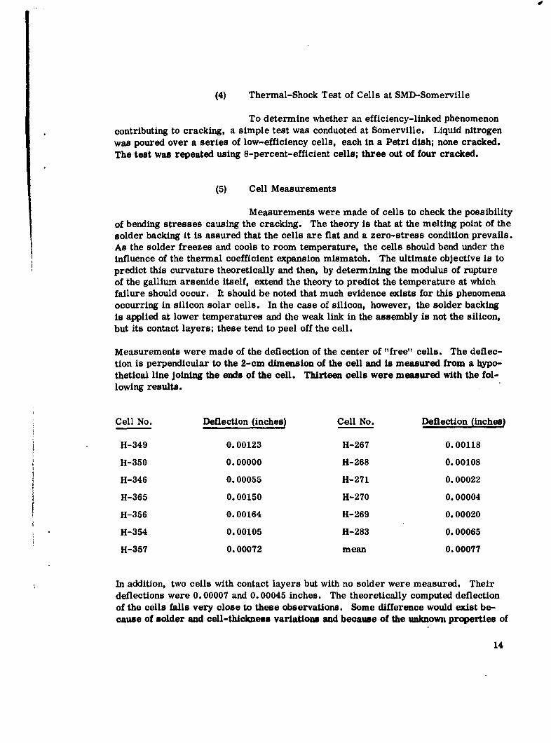
(4) Thermal-Shock Test of Cells at SMD-Somerville
To determine whether an efficiency-linked phenomenon
contributing to cracking, a simple test was conducted at Somerville. Liquid nitrogenwas poured over a series of low-efficiency cells, each in a Petri dish; none cracked.The test was repeated using 8-percent-efficient cells; three out of four cracked.
(5) Cell Measurements
Measurements were made of cells to check the possibility
of bending stresses causing the cracking. The theory is that at the melting point of thesolder backing it is assured that the cells are flat and a zero-stress condition prevails.As the solder freezes and cools to room temperature, the cells should bend under theinfluence of the thermal coefficient expansion mismatch. The ultimate objective is topredict this curvature theoretically and then, by determining the modulus of ruptureof the gallium arsenide itself, extend the theory to predict the temperature at whichfailure should occur. It should be noted that much evidence exists for this phenomenaoccurring in silicon solar cells. In the case of silicon, however, the solder backingis applied at lower temperatures and the weak link in the assembly is not the silicon,but its contact layers; these tend to peel off the cell.
Measurements were made of the deflection of the center of "free" cells. The deflec-tion is perpendicular to the 2-cm dimension of the cell and is measured from a hypo-thetical line joining the ends of the cell. Thirteen cells were measured with the fol-lowing results.
Cell No. Deflection (inches) Cell No. Deflection (inches)
H-349 0.00123 H-267 0.00118
H-350 0.00000 H-268 0.00108
H-346 0.00055 H-271 0.00022
H-365 0.00150 H-270 0.00004
H-356 0.00164 H-269 0.00020
H-354 0.00105 H-283 0.00065
H-357 0.00072 mean 0.00077
In addition, two cells with contact layers but with no solder were measured. Theirdeflections were 0.00007 and 0.00045 inches. The theoretically computed deflectionof the cells falls very close to these observations. Some difference would exist be-cause of solder and cell-thickness variations and because of the unknown properties of
14
the solder at high temperature, i. e. because of creep, the cooling solder may induceno stress in the cell until some temperature below its freezing point. The equationsused to predict this curvature include the solder thickness to essentially the fourthpower. This can explain the wide variation in measured deflections.
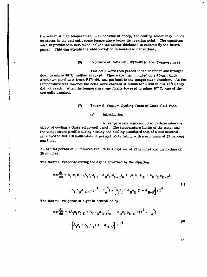
(6) Exposure of Cells with RTV-60 to Low Temperatures
Two cells were then placed in the chamber and broughtdown to minus 80°C; neither cracked. They were then mounted on a 40-mil thickaluminum panel with fresh RTV-60, and put back in the temperature chamber. As thetemperature was lowered the cells were checked at minus 570C and minus 75*C; theydid not crack. When the temperature was finally lowered to minus 970C, one of thetwo cells cracked.
(7) Thermal-Vacuum Cycling Tests of GaAs-Cell Panel
(a) Introduction
A test program was conducted to determine theeffect of cycling a GaAs solar-cell panel. The temperature limits of the panel andthe temperature profile during heating and cooling simulated that of a 240 nautical-mile apogee and 110 nautical-mile perigee polar orbit, with a minimum of 59 percentsun time.
An orbital period of 90 minutes results in a daytime of 52 minutes and night-time of38 minutes.
The thermal response during the day is governed by the equation:
dtmc-d% = ff S+ (Afef *fE +ABeB BE)u + (Afaf 0fE + ABaB#B-E)p
(1)
-A e -6o( A e+ A e(1-08]oB BBBS(T 4 - [s f f BeB B_ T
The thermal response at night is controlled by:
dT 4)dO = (Afefbf_E + ABe BE),u - ABeBOB_ S 7(T 4 -T
- [Afef + ABeB (1- BS)] oT 4 (2)
15

Where:
the mass of the panel (0.1 lb.) is m;
the specific heat of the panel (361 watts per pound per °k) is c;
the areas of front and back surface (9 in2 ea) are Af, AB;
the emissivity of front and back surfaces (0. 75, 0.85) are ef I eB;
the absorptivity of front and back surfaces (0.9, 0.2) are af, aB;
the solar constant (0.9 watts per square inch) is S;
the geometrical shape factors between the front and back surfaces to earth areOf-E' OB-E;
the earthshine at orbit altitude is A;
the shape factor between the back surface and the main satellite is OB-S;
the temperature of main satellite is T ;
the Stefan-Baltzmann constant is a; and
the value of albedo at orbit altitude is p.
Because the solar panel is to be sun-oriented, the quantities "f-E' *B-E' and p aretime dependent in a rather complicated manner and T. is not a known quantity. There-
fore, in this analysis, average values were taken for 0f-E' *B-E' and p and the in-
fluence of the main satellite was neglected. Taking average values will result in acertain amount of variation in the temperature actually experienced from that calculated(approximately k10°C). Neglecting the influence of the main satellite will cause a de-crease in the maximum temperature during the day, since the main satellite will cutoff part of the albedo and earthshine. This influence will be small, however, sincethe solar cell panel is mounted on a thin boom 10 feet away from the vehicle and thusthe vehicle subtends a half angle of 12" while the earth subtends a half angle of 74.
The day and night transient-response equation then becomes:dT=
Day: mc!LT d CI - (Afef + ABeB) o T4 (3)dT
Night: mcL- = C2 - (Afef+ ABeB) arT 4 (4)
where C1 and C2 include the average earthshine and albedo impends. To further ob-tain a better approximation, C1 was chosen at three places in the orbit during the day;at -45e, 90', 135. With these averages the equation becomes:
16
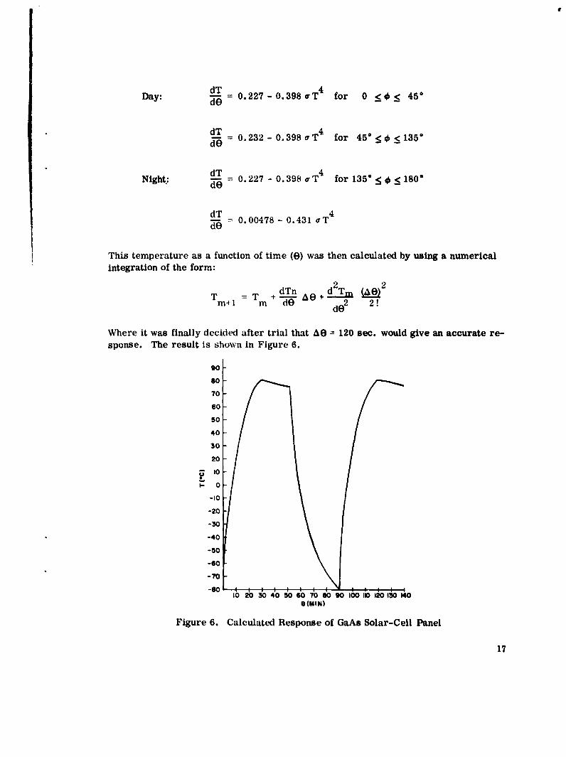
Day:dT 0.227 - 0.398 o T4 for 0 < < 450dT
d = 0.232 - 0.398 a T4 for 45<<1350
dT 4Night.: dO 0.227 -0.398 T for 135 ° 0 < 180
dT= 0.00478 - 0.431 aT 4
This temperature as a function of time (0) was then calculated by using a numericalintegration of the form:
T =T dTn d2Tm (,,)2M+ mA0d 2 2!
do
Where it was finally decided after trial that AO 120 sec. would give an accurate re-sponse. The result is shown in Figure 6.
9060
'70
60
50
40
30
20
10 g0
-10
-20
-30
-40
-50
-60
-70
-6010 20 30 40 50 60 70 S0 90 100 10 120 130 140
O(MIN)
Figure 6. Calculated Response of GaAs Solar-Cell Panel
17

(b) Procedure
Three quartz lamps were mounted 4 inches apart
in a cylindrical shroud 13-1/2 inches in diameter and 18 inches high. Hanging parallelto the three lamps was a 4-x-2-1/2-inch solar-cell panel approximately 4 inches fromthe lamps. During the test, liquid nitrogen flowed through the shroud maintaining acold wall of minus 1550C or less. Micro switches were mounted on a temperaturerecorder with limits set at minus 80°C and plus 800C. These switches controlled re-lays which turned the lamps off and on when the appropriate limits were reached asshown in Figures 7 and 8.
Thermocouples were placed on the board and cell face in various locations to deter-mine temperature gradients through the board during the transient state. These thermo-couples were attached to the surface with aluminized nylon tape.
(C) Results
A comparison of the actual and calculated response
of the panel shows a "flat" in the calculated response. This "flat" was left out during
the actual testing of the panel for it was felt that the information obtained during thesteady state was not of any significant importance in determining the effect of thermalcycling.
ON -OFF SW.
ALARM
0
TROUBLE _
LIGHT
HEATERS 0 MOMENTARYCSW. NC
0
0
/.LS(NO) 110 VACK2 5 3
Figure 7. Low Limit Protection Circuit
18

0 -50 A
11 AVA
X COIL OF K7 IN PARALLEL WITH COIL OF KI
Figure 8. High Limit Protection Circuit
Figure 9 presents the heating-cooling curves for typical cell surface temperature ofthe long and short cycle. The cycles varied in length due to the variation in flow ofliquid nitrogen and to the variation in lamp voltage. The shortest and longest cyclesthe panel was exposed to were 44 and 72 minutes, of which 14 minutes of the shortcycle was heating, and 35 minutes of the long cycle was heating. The panel was sub-jected to a total of 38 cycles with an average total cycle time of 57 minutes.
The calculated rate of temperature change for the first two minutes of heating was 20°Cper minute, where the actual response during test for the same period was 30°C perminute.
(d) Calibration
A panel 6 by 5 inches was divided into 30 one-inch-square blocks. The short-circuit current wals reatd in the center of each of these blockswith a standard solar cell for various lamp voltatges. The voltage was varied in 5-volt
steps from 25 to 60 volts, and it was found that there existed a maximum of 10 percentintensity variation in the solar-cell-panel area of 4 by 2-1/2 inches.
19

+80
+60
+40
V+20
"Ia:
CL
0
-40
-60
-80-t I I I - I - I
0 20 40 60 80 100 120TIME-MINUTES
Figure 9. Actual Response of GaAs Solar-Cell Panel
(e) Re-Evaluation and Modification of the Panel
Upon completion of the thermal-vacuum cycletest of the solar-cell panel, it was decided to restrict the temperature limits the panelwill experience. A new temperature range of minus 150 C to plus 82 0 C was accom-plished by changing the total mass of the panel from 0. 1 to 0.2 pounds, investigatingthe emissivity of the back of the panel, and by revised estimate of the earthshine in-put during the nighttime portion of the orbit. The temperature-time profile (shown inFigure 10) of the panel was calculated in a slightly different manner for the 0.2 poundboard. Using the same equations as previously:
The thermal response during the day is governed by
dt+mc- = Af a S + (Afei.fE , ABeB BE + (AqfE + ABaBoBE)
(1)A,,,e _ o(,4- "r4- [\fef + A: (o- 4_]: ,an
B B 3 Sr - f BB OB2S)]O
20
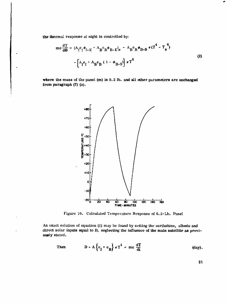
the thermal response at night is controlled by:dT 4 4)
mc- (Afef fE + ABeB BE) - ABeBbBS u(T 4 - T 4
-[Afef + ABeB (1 - "B-S)]) T4 (2)
where the mass of the panel (m) is 0.2 lb. and all other parameters are unchangedfrom paragraph (7) (a).
+8o
+70
+60
W
4+40
2 +30-
+20-
0
-10
-201 I I I0 20 40 60 80 l00 120 140 160J
TIME-MINUTES
Figure 10. Calculated Temperature Response of 0.2-Lb. Panel
An exact solution of equation (1) may be found by setting the earthshine, albedo anddirect solar inputs equal to D, neglecting the influence of the main satellite as previ-ously stated.
Then D-A ef+eB aT4 = mc d- (day).
21

Rearranging and integrating:
t= M3 tanh-1 T ta+-t2Cv 1 T (Daytime equation).
2CD UD D1
Limits of integration
When t= 0 T= T
t =tD T =Tf
/2CD 3 Tf = [-1 TT T,
tanhC- +f tan -j[tanhlT, + tan
(Daytime equation).
Let the nighttime input N include only the earthshine, neglecting the effect of the main
satellite; then from equation (2)
l t 4 dTN = A ef+eBB4 = mc dT
Solving for t =
--1T 1In (Nighttime Equation)2CN3 N T + CNN
Limits of integration:
t = tD when T = Tf
t = tO (orbit time) when T = T
or
ta N In 1 iN C3 C 2 T +C N(CN2 T +CNI
2C D3 N + f T+ N N + N n
Nighttime equation where tN = night orbit time = (t0 - td)
22
Evaluation of the shape factors for day and for night was accomplished by plotting thevalues at various positions around the orbit, drawing a smooth curve through thesevalues, and finding the area under the curve as the average shape factor. The results
of this may be seen in Figure 11.
As a result of the difficulty encountered during the instrumentation of the panel it hasbeen decided to design a circuit that will utilize the silicon wafer as a temperature-measuring device. A circuit has been designed (shown in Figure 12) such that thewafer will have the same output as a eopper-constantan thermocouple. Thus the wafer,which is bonded just behind a solar-cell, can be used in conjunction with a standardcopper-constantan temperature recorder to control the temperature limits achievedby the panel during the test cycles.
Investigation of the back-surface finishes for a 0.2-pound panel gave the following re-sults:
a e Tmax Tmi n
0.2 0.85 +82°C -150C
0.15 0.7 +900C - 8"C
0.08 0.1 +115"C +140C
(8) Conclusions
The following tentative conclusions can be drawn, based
on experimental data and analysis:
1. Gallium arsenide cells, as presently made, withor without soldered leads, can withstand thermalcycling from plus 80"C to minus 80"C with a tem-perature rate of change of 30"C per minute.
2. Materials suitable for silicon cell arrays are notsuitable for GaAs cell arrays when subjected tothe thermal conditions specified in 1 above, be-cause of the inherent weakness of GaAs as com-
pared with silicon.
3. Experimental data and analysis indicate that withproper choice of array materials, GaAs solarcells on a panel can be made to withstand tem-perature limits above 80"C and below 15"C, and
a rate of temperature change in excess of 11Cper minute.
23

0% z
-. -. 0
31w 0
0 EO. 0V)LA LL 0
0
0 0
4
w IhJ0 Q0
w 4h -i
z 9L
0 UWa~U (.0i
M 0
0 0
x 4Z (nWZ O0
224

RESISTANCE
BRIDGE oWAFER
D.C. Ioo, 10 TURNM I LLIVOLT HELIPOT
POWER R2 RI
SUPPLY
MILLIVOLTMETER
Figure 12. Circuit for Use of Silicon Wafer as Temperature-Measuring Device;Schematic Diagram
4. The inherent weakness of GaAs can be overcomeby designing a proper combination of solder pat-terns and/or thickness and cell thickness. Bythis means, GaAs cells on a panel can be fabri-cated to withstand more severe temperature limitsand temperature-time profile than plus 82*C tominus 15°C and li°C per minute.
5. The power-to-weight ratio for the present orbitalpanel is 1. 65 watts per pound. This ratio can besignificantly increased by additional effort in this
area.
As noted previously, these conclusions are tentative and more work is required In theseareas in order to positively establish the limits of a GaAs cell solar panel.
4. Adhesive Work
The RTV-60 silicone-rubber adhesive, used to mount cells on arraysbuilt to date, has successfully withstood all environmental tests. In addition, its history
25

is well known since it is used on a number of other types of solar-cell arrays. Inlight of this, no further adhesive-study work is contemplated for the orbital panels un-less subsequent qualification tests indicate otherwise.
5. Soldering Techniques
Three techniques have been successfully used to date. The first is astraightforward application of conventional techniques with two exceptions; no flux isused and, to minimize thermal cracking, soldering-iron temperatures are reduced toa minimum. This method used 63/37 eutectic tin-lead solder and is hereafter called"low-temp" soldering. A tentative specification has been generated covering the tech-nique; yields have been about 90 percent with the balance lost due to thermal cracking.
The second technique is the same as above except that the cell is placed on a hot plateat 100°C to 120°C and the soldering is done there. For approximately 30 cells donethis way, thermal cracking has been eliminated.
The third technique is the same as the second except that the hot plate is at 2000C to220°C and the solder used is the same composition as that on the cell back, i.e., 95.5percent lead, 2.0 percent indium, 1.5 percent silver, and 1.0 percent tin. This iscalled "high-temp" soldering. Thermal cracking has been virtually eliminated by thisprocess.
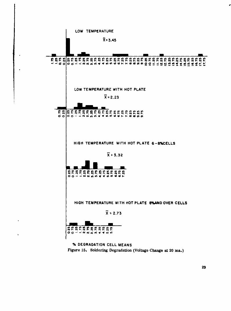
Figures 13 through 15 show another measure of soldering success. The differencesbetween the soldering techniques (as far as short-circuit-current change are con-cerned) may be statistically significant. Additional samples are required in order tomake a positive statement in this regard. The physical significance is not as yetunderstood. The other parameters appear to show no significant difference. Onepoint that should be noted is the spread of the short-circuit soldering degradation datain Figure 15. This is simply explained by the characteristics of the current-voltage(I-V) curves; the measured parameter (voltage at 20 ma.) is in the region of the aver-age maximum power point. The slope of the curve in this region is changing rapidlyand in addition there are differences in the shape of the I-V characteristic from cellto cell. Accordingly, depending on the efficiency and shape of curve, small changesfrom the short-circuit current valve may produce small or large changes in voltage.
Peel tests have been conducted on "low-temp" connections. In all but a few cases, thecell ruptured, or occasionally, the lead wire failed. As previously reported, therewere however, a few cases where the silver "P" strip peeled. Neglecting these fewcases, the tests indicate that the gallium arsenide cells should present no problemswith peeling of contact layers during temperature cycling. The interesting fact hereis that in performing peel tests on silicon cells, failure almost invariably occurs bypeeling of the same contact layer that peels during temperature cycling. This lendscredence to peel testing as a measure of the ability to withstand thermal cycling.
26

LOW TEMPERATURE:0.95
LOW TEMPERATURE WITH HOT PLATE
X 4.65
HIGH TEMPERATURE WITH HOT PLATE
6-8% CELLS
= 6.85
HIGH TEMPERATURE WITH HOT PLATE
8% AND OVER CELLS
X: 3.86
a P f fyf-CV -- N - N W- I- tyf NW-fl 4
%DEGRADATION CELL MEANS
Figure 13. Soldering Degradation (Short-Circuit Current)
27

LOW TEMPERATURE
X 0.60
4 nJ- Ncm C4 fe4 N( N N f- NV.- dNI-
LOW TEMPERATURE WITH HOT PLATE
X 0.74
HIGH TEMPERATURE WITH HOT PLATE6-8% CELLS
X= 1.77
HIGH TEMPERATURE WITH HOT PLATE8% AND OVER CELLSX= 0.73
% DEGRADATION CELL MEANS
Figure 14. Soldering Degradation (Open-Circuit Voltage)
28
LOW TEMPERATURE
X3.45
LOW TEMPERATURE WITH HOT PLATE
X2.23
Co d 6-c pi ri4 0o .:ad46
HIGH TEMPERATURE WITH HOT PLATE 6-8%CELLS
x3.32
HIGH TEMPERATURE WITH HOT PLATE B%AND OVER CELLS
R 2.73
in In in in
% DEGRADATION CELL MEANSFigure 15. Soldering Degradation (Voltage Change at 20 ma.)
29

One possible anomaly has been detected to date. In either high- or low-temp hotplatesoldering of cells with efficiencies less than 8 percent, thermal cracking has beencompletely eliminated. Approximately 75 cells have been done this way. To date,ten 8-percent cells have been high-temp soldered. Two of these have thermallycracked. It is not as yet clear whether this is pure chance, an inadvertent changein soldering procedure, or whether this is in some way associated with high efficiency.Additional samples are required in order to draw a definite conclusion.
C. Radiation Testing
1. Electron Irradiation
a. Introduction
Gallium arsenide (GaAs) and silicon (Si) n-on-p solar cellswere irradiated with 0. 8- and 5. 6-Mev electrons in the continuing study of the effectof particle irradiation on these devices. The experiments were performed on theRCA 1-Mev Van de Graaff generator and the 6-Mev linear accelerator at the plant ofEthicon Products, Somerville, N. J. The conditions of operation for the experimentsare listed in Table 1L.
TABLE III.
OPERATING CONDITIONS OF ELECTRON IRRADIATIONS
Parameter 0. 8 Mev Experiment 5.6 Mev Experiment
Machine 1-Mev Van de Graff 6-Mev Linear Accelerator
Ambient Condition Vacuum . 2 x 10 - 5 Airmm Hg
Cell Position Perpendicular PerpendicularRelative to Beam
Beam Current Steady; Maximum Pulsed. Pulse width: 5 ju s;value of 0.23 M a Pulse repetition rate:over area of 400 cps. Average cur-0.63 cm 2 rent: 10 u a over area
of 26. 1 cm 2
Maximum Temperature 80*C 60*C (estimated)Rise in Cell Duringbombardment
30

The measurements made included the sunlight efficiency and spectral response beforeand after bombardment as well as during the experiment. The light source consistedof an incandescent lamp, a filter of one inch of water with 7/16-inch of heat-absorb-ing glass, and eight interference filters spanning the spectral range of from 1. 25 to
3.06 Mev. Sunlight measurements were also made during the 0. 8-Mev experiment tocheck the effectiveness of the filtered incandescent source in predicting the perform-ance in sunlight.
b. Description of the Cells
The silicon (Si) cells were of the n-on-p variety, obtained fromthe RCA Semiconductor and Materials Division (SM & D) at Mountaintop, Penna. Thegallium arsenide (GaAs) cells came from the SM & D at Somerville, N. J.
The initial properties of these cells are listed in Table IV; the Si cells are designatedby the prefix MT and the GaAs cells by S.
c. Results of the 0. 8-Mev Run
These results are expressible in terms of the maximum poweroutput of the cells versus flux, and the critical flux (0c) required to reduce the poweroutput by 25 percent. The spectral response curves were not analyzed to yield theouter-space response inasmuch as previous work has shown that outdoor measure-ments are a good indication of outer-space response.
Another objective of this experiment was to compare the response obtained from thefiltered incandescent light (with the one-inch of water and 7/16-inch of heat-absorbentglass) with that observed in sunlight during the tests. Inasmuch as the sun positionat this time of year is far from normal with respect to the test area, measurementswith the cells horizontal (required because the Laboratory pyrheliometer is a hori-zontal detector) are subject to errors of 10 to 20 percent. A further comparisonwas therefore based upon the initial measurement made earlier and final measure-ments made after bombardment; these measurements were made with the normal-incidence pyrheliometer at the Astro-Electronics Division (AED) of RCA. Thesereadings, together with the curve obtained from the filtered incandescent source,were used to predict the sunlight performance. A comparison of the various measure-ments (in terms of the critical flux), as well as the performance of GaAs and Si cells,is given in Table V. All the cells listed in Table IV are not listed in Table V sincecertain of them broke or otherwise changed, preventing further analysis.
31

TABLE IV.
INITIAL PROPERTIES OF SOLAR CELLS
Cell Initial SunlightNo. Efficiency ()Electron Irradiation
MT-0 10. 2 0. 8 Mev
MT-J4 10. 5 0. 8 Mev
MT-265A 10. 1 0. 8 Mev
MT-4A 9. 7 0. 8 Mev
MT-13A 9. 1 0. 8 Mev
S79-A 8. 2 0. 8 Mev
S12A 8. 4 0. 8 Mev
S14HA 8. 2 0. 8 Mev
S14HC 8. 3 0. 8 Mev
S164#1 -0. 8 Mev
MT-I 10. 2 5. 6 Mev
MT-5B 9.2 5. 6Mev
MT-11B 9.5 5.6 Mev
S12B 8. 0 5. 6 Mev
S79B 8.4 5. 6Mev
S14HB 7.8 5. 6Mev
32

TABLE V.
CRITICAL FLUX OF GaAs AND Si CELLS
Cell Oc (e/cm2 )
No. Filtered Incandescent Sunlight Measurements Initial and FinalData During Bombardment Sunlight Measurements
MT-J4 1.0xl0 15 5.4x10¹⁴ 1. lx10 1 5
MT-4A 9.3x10 1 4 9.3x101 4 1.3x10 1 5
MT-13A 1.2x10 15 6. 2x10 1 4 1.4x10 1 5
S79A 1.5x10¹⁵ 1. lx1015
S12A 1.4x101 5 1. 1x10 1 5
S14HC 1.Oxl01 5 8.5x10¹⁴ 1.Oxl015
There is good agreement between the various values of Oc, particularly for the fil-tered incandescent data and for the initial and final sunlight measurement. The Ocobtained from the sunlight measurements during bombardment is generally lower thanthat from the filtered incandescent data which is not usually the case. However, thesunlight measurements may be in error by 10 to 20 percent because of the large in-cidence angle of the sun's rays. The data in Table V is sufficiently significant,nevertheless, to warrant further comparisons between the filtered incandescent lightand sunlight.
The relative power outputs of Cells No. MT-J4 and S14HC are shown in Figures 16and 17 and illustrate the performance with the different light sources. The data fromthe filtered incandescent source is reasonably consistent with the sunlight data.
A comparison of power outputs from a Si cell and a GaAs cell is illustrated in Figure18. The curves are based on the initial and final normal-incidence measurements insunlight; they do not cross over primarily because the GaAs cell is less efficient.However, even if the GaAs cell were of the same efficiency as the Si cell, their per-formance would only be comparable up to flux values of 1015 electrons per squarecentimeter; at higher values, the Si cell would be superior because of its moregradual decrease in power output.
33

1. 0
0.6
0.6 0.8 Mav ELECTRONS x*FILTERED INCANDESCENT DATA
6 - x SUNLIGHT READINGS DURING BOM1BARDMENT
SBASED ON INITIAL AND FINAL
0.2
10"3 1014 Ila" 1O4
*(s/cm)
Figure 16. Comparison of Relative Power Output and 0for Cell No. MT-J4
I1.0 X x
0.6
0.6 -0.8 Mew ELECTRONS*FILTERED INCANDESCENT DATA
9116 x SUNLIGHT READINGS DURING BOMBARDMENT61BASED ON INITIAL AND FINAL
0.4 NORMAL- INCIDENCE READINGS
IN SUNLIGHT
0.2
0Iola 1014 logs 104
* .cm'e)
Figure 17. Comparison of Relative Power Output and 0for Cell No. S14HC
34

IS I I I I I I
14
_9- X\ AT-13A
a. - 0.8 Mev ELECTRONS 9. --
. am I AREABASED ON SUNLIGHT READINGS
10 / XI0 -/
Go As$12-A X
S -0.4%
6 I I I , I I
10" i 104 00 "0i**./cm t )
Figure 18. Comparison of Power Output and Flux for GaAs and Si Cells
The change in these cells as a result of the total flux (OT) is shown in Table VI interms of the ratio of the final values of output power and short-circuit current to theinitial values. The data is based on the final values measured at normal incidencein sunlight.
The percentage of decrease in the normalized power output of the Si cells per decadeof flux in the linear region of the semi-logarithmic plots averaged 22 percent for sun-light and 25 percent for filtered-incandescent light. These values are comparablewith those found by other workers but differ from the values reported for the 17. 6-Mev proton irradiation. The inference is reinforced that annealing occurred in the17. 6-Mev run.
A comparison of the above results was made with the results of experiments conduct-ed over a year ago on experimental GaAs and Si n-on-p cells. The conclusion at thattime, in agreement with the present results, was that the GaAs and Si cells werecomparable in radiation resistance to 0. S Mev electrons. However, the average 0c(based on filtered-incandescent-light data) was 2. 3 x 10¹⁶ electrons per squarecentimeter for GaAs cells and 6. 2 x 10¹⁵ electrons per square centimeter for Si cellswith one-ohm-per-centimeter base material. (See Reference 1). The difference inthese values of Oc from the present ones is ascribed to improvements in both cells.
35

TABLE VI.
RATIO OF FINAL TO INITIAL VALUES BASED ON SUNLIGr 7 MEASUREMENTS
Cell OT 2 If/Ii Pf/PiNo. (e/cm ) M (%)
MT-0 3.0x10 15 71 62
MT-J4 3.0x10 15 73 64
MT-4A 2. 8x101 5 77 68
MT-13A 2. 9x10 1 5 70 68
S79A 3.2x10 1 5 53 50
S12A 3.3x10 1 5 64 56
S14HC 3.0x10 1 5 46 38
For example, the smaller Oc in present GaAs cells may be uw to a larger minority -carrier lifetime and/or a larger constant (C) relating the flW"Wud lifetime (r) asfollows:
TO
1+ Cr '0
where To is the initial lifetime. To separate these two effect t. the effective energyrequired to create an electronhole pair (which is subsequentyoco1lected) was deter-mined for an old experimental cell and a current cell, usingls5-a5-kev electrons. Thevalue for the experimental cell was 120 electron volts per cellcroected pair (typical ofvalues in the past) while that of the present-day cells is 42 eettltrn volts per collect-ed pair. The effective energy required to create an electroi.oII0e pair, which iscollected, is inversely proportioned to the sum of the diffusijleI lengths on both sidesof the junction. Present-day cells have a total diffusion lengstlt three times largerthan the experimental cells; consequently, the lifetime is improvoved by a factor of 10.
The lower 0 c found in present-day cells cannot, however, bec0orompletely explained onthe basis of the improved lifetime; this parameter will only Ucco-ount for a factor oftwo to three. An increase in the value of the constant relatilirlIifetime and flux by afactor of five must therefore be postulated, signifying the preWence of another defectwhose presence was not previously seen.
The Oc of the experimental cell was in excess of 4.6 x 10¹⁵ elKItrons per square centi-meter in support of the contention that the characteristics of GW 0 - cells have changed.
36

d. Results of the 5. 6-Mev Run
Measurements made on the cells during this portion of the ex-
periment were substantially the same as in the previous portion. Values for Oc basedon filtered incandescent light, and on initial and final sunlight are listed in Table VII.The two values of 0c are in rather close agreement.
The average decrease in power output per decade of flux for the normalized semi-logarithmic plots for the Si cell power output is 23 percent for the filtered incande-scent light and sunlight data. Figure 19 compares the power output of the Si and GaAscells as a function of flux; the curves are based on the initial and final sunlightmeasurements. The GaAs cells are shown to be clearly superior with greater powerfrom 101 3 to 1015 electrons per square centimeter; Oc is larger for GaAs cells thanfor Si cells by a factor of 10. An interesting fact is that the general behavior shownin Figure 19 agrees with that obtained in the 17. 6-Mev proton irradiation tests.
The change in these cells because of total irradiation is listed in Table VIII; the dataare expressed in ratios of final to initial values of power output and short-circuitcurrent in sunlight.
II I I I I I I I I
',% x
12-
50
5.6 Mev ELECTRONS S 798
0 - . CM2AREA 11.4 %
BASED ON SUNLIGHT \
READINGS MT-11l9.5%
4I I10 10 104 0I
(9/cm')
Figure 19. Comparison of Power Output and Flux for GaAs Cells
37
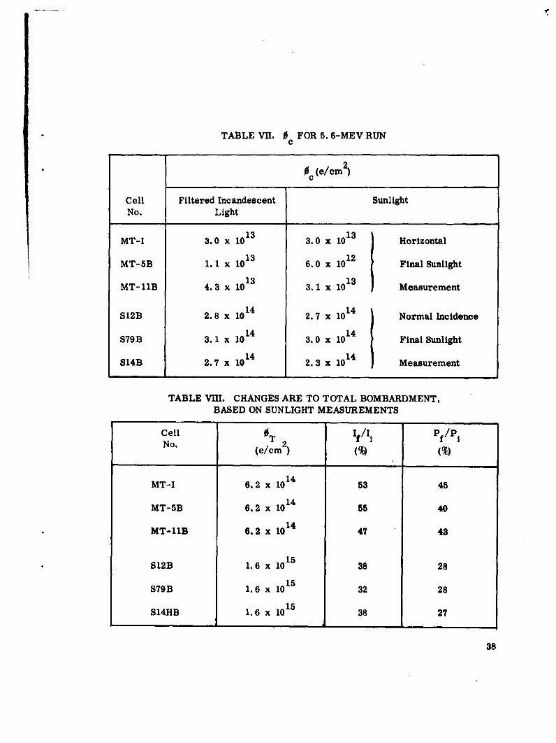
TABLE VII. 0 FOR 5.6-MEV RUNC
0 (e/cm )
Cell Filtered Incandescent SunlightNo. Light
113 13MT-I 3. 0 x 10 3. 0 x 10 Horizontal
MT-5B 1. 1 x 10¹³ 6. 0 x 1012 Final Sunlight
MT-11B 4. 3 x 10 3. 1 x 10¹³ Measurement
S12B 2. 8 x 10¹⁴ 2. 7 x 10¹⁴ Normal Incidence
S79B 3.1 x 10¹⁴ 3.0 x 10¹⁴ Final Sunlight
S14B 2.7 x 10¹⁴ 2.3 x 101 4 Measurement
TABLE VIII. CHANGES ARE TO TOTAL BOMBARDMENT,BASED ON SUNLIGHT MEASUREMENTS
Cell 0 T If/Ii Pf /PiNo. (e/cm2) (%) M
MT-I 6.2 x 101 4 53 45
MT-5B 6.2 x 10¹⁴ 55 40
MT-1IB 6.2 x 101 4 47 43
S12B 1.6 x 10¹⁵ 38 28
S79B 1.6 x 10¹⁵ 32 28
S14HB 1.6 x 10¹⁵ 38 27
38

e. Discussion of Results and Conclusions
The conclusions arrived at as a result of the experiments areas follows:
(1) GaAs and Si cells are comparable in radiation resistanceto 0. 8 Mev electrons for fluxes of up to 1015 electrons per square centimeter; abovethis, Si cells are superior by virtue of the more gradual decrease in power outputwith increase in flux. The Oc for GaAs is 1. 1 x 10¹⁵ electrons per square centi-meter and for Si 1.3 x 10¹⁵ electrons per square centimeter, based on sunlightmeasurements.
(2) The properties of present-day GaAs cells are superiorto those of a year ago; specifically, the minority-carrier lifetime is one order ofmagnitude higher.
(3) The relative performance of GaAs and Si cells is ac-curately determined although there is some question concerning the flux scale in the5. 6-Mev experiment; the GaAs cells are ten times better in radiation resistance thanthe Si cells. Based on sunlight measurements, Oc is 2. 7 x 10¹⁴ electrons per squarecentimeter for GaAs cells and 3 x 101 3 electrons per square centimeter for Si cells.However, the Si cells will deliver more power for flux levels greater than 1015
electrons per square centimeter.
(4) The Si cells degraded 40 times faster at 5. 6 Mev thanat 0. 8 Mev; the GaAs cells degraded only four times faster.
(5) The performance of the cells in sunlight is reasonablyclose to that in the filtered incandescent light; this is to be expected inasmuch as theuse of heavy filtering causes an incandescent light spectrum to approach the sunlightspectrum.
Those of the items listed which merit further discussion are the ones concerning therelative performance of GaAs and Si cells and the greatly enhanced rate of damagein the Si cells at 5. 6 Mev.
It has been established that GaAs cells are initially superior to Si n-on-p cells whenirradiated with 1. 8, 17. 6 and 95.5 Mev protons. (In all cases, the Si cells eventual-ly outperform the GaAs cells by virtue of their more gradual drop in power outputwith increase in flux.) It is intuitively expected, therefore, that the initial super-iority would also be evident in the case of electron irradiation. This expectation wasrealized in the case of the 5.6-, but not the 0. 8-Mev experiment. Questions ariseas to whether this behavior is attributable to a distribution of defects or to the typeof defect introducted.
39

The rapid damage in Si cells at 5. 6 Mev compared to that at 1 Mev also requires ex-
amination since it was not expected and since it is a factor in the comparison ofGaAs and Si cells. The cross-section for producing a primary defect in Si has beencomputed by H. Flicker using the relativistic McKinley-Feshback formula. Thecross-section is 65 barns for 1-Mev, and 76 barns for 6-Mev electrons. Further-more, the numbers of secondary defects per primary displacement is around 1. 3 for1-Mev, and 2. 1 for 6-Mev electrons. Consequently, the damage rate at 6 Mev shouldonly be twice as large as that at 1 Mev, but a factor of forty is obtained. The ques-tion resolves itself then as to whether this increased rate is due to the introductionof another defect or to failure of reciprocity, I. e. the resulting damage depends notonly on the integrated dosage but also on the magnitude of the beam intensity. Thislatter item merits consideration because of the pulsed nature of the 5. 6-Mev irra-diation. Conceivably, if non-reciprocal effects were occuring in the Si and not in theGaAs, much of the relative advantage of GaAs at 5. 6 Mev could disappear if the ir-radiation were performed at lower beam intensities.
The failure of reciprocity in Ge has been noted for 0. 5-Mev electrons when the peakbeam current exceeds 20 ma per square centimeter. At a peak current of 200 maper square centimeter, the damage rate was seven times higher than that at 20 maper square centimeter. (See Reference 3). A comparison of the peak-current den-sity in the 5. 6-Mev experiment to the values quoted above is difficult since each ofthe main 5 ps pulses itself consisted of a large number of microwave pulses. A lowerlimit to the peak current density given by the duty ratio of the 5 jMs pulse is 0. 19milliamperes per square centimeter. The upper limit is probably less than 20 mil-liamperes per square centimeter because the peak power required from the machinewould then be in excess of 3 megawatts. Hence, based on the experience with Ge,It is doubtful that non-reciprocity can be invoked to explain the high damage rate inSi cells for 5. 6-Mev electrons.
The other possibility for explaining the high rate is the introduction of another defect.Such a defect may be the divancy, an intrinsic defect consisting of two vacant, near-est-neighbor, lattice sites. (See Reference 4). Although it is produced at a rate ofapproximately 5 percent of the vacancy-production rate for 1. 5-Mev irradiations, itis more efficiently produced at higher electron energies (Reference 4). Further ex-perimental work at various electron energies is required to resolve these questionsconcerning the damage rate in Si solar cells.
The differences seen in the relative rates of damage in GaAs and Si solar cells with
electron and proton irradiation may result either from the damage distribution effectsor the introduction of different defects in electron and proton irradiations. Thedamage produced by high-energy protons is expected to be uniform throughout the ac-tive regions of the GaAs and Si cells. * The damage is also more complex than in the
*The active region extends from the surface to a depth of 150u in Si cells and no
more than 5 ju in the GaAs cells.
40
case of an electron irradiation since the protons can transfer more energy to thelattice atoms. Even in the case of electron irradiations, however, approximatelyuniform damage is expected in the active regions of these cells provided the electronenergy is much greater than the threshold energy for damage. For example, Flickerhas shown that the damage rate in Si due to 0. 5-Mev electrons decreases by only afactor of two for the first 1 0 0 u, of Si (Reference 5). The change in rate will be evensmaller for 0. 8-Mev electrons. Almost no change in rate can be expected in GaAscells since the active region is so small. For any energy above the threshold, thedamage will be effectively uniform in GaAs cells. Also arguing against distribu-tional effects is the results of the 1. 8-Mev proton irradiation. These protons have arange of approximately 2 mils in Si and less in GaAs, yet the GaAs cells are moreradiation-resistant than the Si cells by a factor of 10 or more. The possibility isindicated that different defects in the proton and electron irradiations are responsiblefor the observed performance of GaAs and Si cells.
f. References
(1) Final Triannual Report, Semiconductor PhotovoltaicConversion, DA36-039-SC-87417; Report Date: November 30, 1961. (Signal Corps,U.S.A.)
(2) F. Seitz and J. S. Koehler "Displacement of AtomsDuring Irradiation," Solid State Physics 2, Academic Press, Inc. (1956), p. 382.
(3) P. Baruch, "The Use of the Electron Accelerator inSolid State Physics," Nuclear Inst. and Meth. 11, 196(1961).
(4) J. W. Corbett and G. D. Watkins, 'Silicon Divancyand Its Direct Production by Electron Irradiation, " Phys. Rev. of Letters 7314(1961).
(5) H. Flicker, Private Communication.
2. 1. 8-Mev Proton Irradiation
Three GaAs cells were irradiated with 1. 8-Mev protons at Ohio StateUniversity. The initial efficiency, critical flux (0 c), and ratio of final to initial valuesof short-circuit current and efficiency as a result of the total irradiation (OT) arelisted in Table IX. All of the solar-cell parameters are based on sunlight measure-ments.
The critical flux is three to four times smaller for 1. 8-Mev protons than for 17.6-Mev protons. A reduction is expected because of the energy dependence of the damage
41
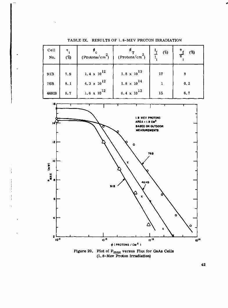
TABLE IX. RESULTS OF 1. 8-ME V PROTON IRRADIATION
Cell 17. 0 0 f M '7
No. M% (Protons/cm ) (Protons/cm ) . 7
76B 8.1 4. 3 x10 12 1. 8x10 141 0.2
46HB 8.7 1. 6 x 10 12 6. 4 x 10 1315 6.7
1.8 M.EV PROTONSAREA: 9z.8 CM2
BASED ON OUTDOORMEASUREMENTS
I00
46H
44

introduction rate and also because of the defect distribution. Protons with 1. 8-Mevenergy are far less penetrating than 17.6-Mev protons, hence damage is producedcloser to the surface where the predominant photovoltaic response of GaAs occurs.The reduction in Oc is somewhat smaller than expected; however, a reduction by afactor of ten would be implied, for instance, by a l/E dependence of the introductionrate such as found in Si cells.
The defect-distribution effect is evident from the drastic reduction in short-circuitcurrent and efficiency as a result of the total irradiation. This effect is more evident
in the efficiency degradation which includes both the short-circuit current and open-circuit voltage degradations. Obviously there was a sizeable drop in open-circuitvoltage.
Curves of the maximum power output as a function of flux are shown in Figure 20.Although Cell 76B was irradiated with 1. 9 Mev protons, its curve is representativeof the results obtained at 17.6 Mev. By comparison, the curves for the other twocells show the effect of the defect distribution and energy dependence of the introduc-tion rate.
D. Thin-Film Gallium Arsenide Investigation
1. Introduction
The work described in this section was undertaken in an attempt tofabricate thin, single crystal films of gallium arsenide (GaAs) on a germanium (Ge)substrate as a possible use as a major cost reduction technique for the GaAs solarcell. Since the active part of a solar cell extends only for several microns belowthe surface, a GaAs layer no more than 10 microns thick supported by a much thicker,lower cost, single-crystal wafer of Ge should be a feasible device structure. TheGe would also act as a low-resistance ohmic contact.
The initial technical approaches to this work center on an evaluation of methods fordepositing epitaxial films of GaAs on Ge, techniques for producing the desired dopingstructure, and studies of the resultant photovoltaic and surface contacting properties.
2. Methods of Producing GaAs Films
Three methods for producing single-crystal films of GaAs on Ge arecurrently being used. The first, shown in Figure 21, utilizes a stream of hydrogen(H2) gas which passes over a source of GaAs at a temperature of about 900"C. Ar-senic enters the flowing H2 quite readily, while the Ga is most probably carriedalong as GaO by traces of oxygen or water vapor in the H2 .
43

Go As GERMANIUMWAFERS
N2 GAS ~ QUARTZ /N1SUPPORTS
Ta 9000 C T= 75 0 *C
Figure 21. Schematic Drawing of Apparatus for Forming GaAsFilms on Germanium Using GaAs as the Source Material
The GaAs deposits on the Ge at about 750°C. One serious drawback to this methodis that the production rate is quite slow, most probably due to the distance betweenthe source and the substrate. Film growth rates are about 1/2 micron per hour;several days are required for a run and only three to four wafers of Ge can be usedin the apparatus at one time. The second method, as in Figure 22, involves the pas-sage of gases over the elements Ga and As rather than over GaAs. Here, the H2stream flows over elemental As at one end of a quartz 'Tee", a hyrdogen and bro-mine (Br) stream flows over elemental Ga at the other end of the 'Tee" (the Ga thusbeing transported as Ga Br), while the formation of GaAs on the Ge takes place inthe center stem of the 'Tee". The temperatures are controlled separately at eachregion. The heaters are so designed that a constant-temperature region exists atthe position of the Ga, As and Ge wafers. Bromine is used because preliminary testshave shown that it is purer and more easily controlled than anhydrous hydrogenchloride (HC1) which is more commonly used as the chemical reactant for this type ofreaction. Preliminary runs have been made and have proven the apparatus to be sat-isfactory. The temperature of the As was 4150C, that of the Ga was 7950C and thatof the Ge wafers was 595"C. Growth rates of the GaAs are about five to ten micronsper hour.
The third method used successfully for growing GaAs films on Ge involves heating aflat wafer of GaAs in a graphite boat to temperatures of 8500C to 950 ° C. The Ga andAs are transported in an 112 atmosphere (by mechanisms essentially identical to thoseused in method 1) and deposit on the Ge wafer now situated much closer to the GaAssource. Layers can be grown at the relatively rapid rate of about 1 mil per hour.
3. Discussion of Results
Studies of appropriate doping structures and procedures have beenfound to be dominated by two facts. The first is that whenever Ga and As are depositedsimultaneously on Ge, a thin degenerate p-type Ge layer is formed at the surfacebecause Ga has the highest solubility of any impurity in Ge and diffuses much more
44

z -0 a0a
LU00.
4
04.Jx
IL. L. w
4 U)P
LU-i
4Z002
U) C
-Id
wl 0
0 JW
I-.-4ZW4
2>d
XUU) 45

slowly than As. Thus, in order to avoid a junction in the Ge substrate or at the GaAs-
Ge interface, p-type Ge (already degenerate) must be employed, and the GaAs in
contact with the Ge must be p-type. This, in turn, dictates that the photovoltaic ele-
ment in the GaAs film must be an n-on-p device. The second fact is that since GaAsand Ge are eutectic at 8780C, very serious limitations are placed on the diffusion
temperature of the dopant impurity (and therefore the dopant impurity itself) avail-able for achieving an appropriate doping structure. Thus, obtaining the appropriatedoping during the film growth rather than afterward is important; our present worktakes both these facts into account. For example, all our Ge substrate material isp-type, Ga doped, and has a resistivity of 4 x 10- 4 ohm-centimeter.
Several GaAs single-crystal films ten to thirty microns thick have been prepared usingthe method illustrated in Figure 21. These have almost always been n-type, even when
a p-type GaAs source has been used. Although some photovoltaic effects have beenobserved with these films (0. 25-volt open-circuit voltage and 10 to 20 milliampereper square centimeter short-circuit current) the wavelength response of these ef-fects begins at a photon energy of 0.68 ev, thus indicating that these are not due tojunctions within the GaAs, but that at least one side of the photovoltaic element is Ge.Several GaAs films one to three mils thick have also been grown by the third methoddescribed. These films, too, are invariably n-type even when the source wafer ofGaAs is heavily doped with Zn and Cd (1020 and 4 x 10¹⁸ atoms per cubic centimeterrespectively). In order to pudy this lack of control over the doping of the films dur-ing growth, radioactive Zn and Cd1 1 5 are being used in tracer experiments. Thevery interesting initial results have shown that the amount of Zn or Cd in the depositedfilms is about 103 less than that in the source wafer.
In support of a program directed toward the fabrication of a solar cell consisting of athin polycrystalline layer of GaAs on which a photovoltaic metallic contact is evap-orated, metallic contacts to single crystal GaAs are being investigated. Such photo-voltaic metallic contacts on single crystal n-type GaAs have been prepared usingevaporated films of silver (Ag), platinum (Pt), and chromium (Cr). In order to ob-tain a useful photovoltaic response, such contacts must possess a relatively largebarrier height (ideally approaching the bandgap). In addition, the metallic film mustpossess a high optical transparency simultaneous with a low electrical-sheet re-sistivity. For these reasons the measurements during this quarter have been confinedto the determination of contact-barrier heights and current-voltage characteristics,the evaluation of the physical characteristics of the metallic film, and comparativephotoresponse measurements using a focussed microscope lamp.
Three independent methods of measuring the contact-barrier height have been used.One is the differential capacitance method which, under proper conditions (Reference1), provides an accurate measurement of the barrier height in terms of the voltagedependence of the inverse square of the barrier capacitance. This method is illus-trated in Figure 23, for a Ag-GaAs contact. The barrier height may also be measured
46

2.0
Ia2W
1.0 -go
-. 2.0 -. 0 0 I.0
V (VOLTS)
1 2
Figure 23. Plot of ( ) versus Voltage for Ag-GaAs Contact
by measuring the wavelength dependence of the photoemission of electrons from themetal into the semi-conductor (Reference 2). lowever, since this method is accurateonly over a restricted range of barrier heights, it has not been useful with the GaAscontacts prepared to date. The current-voltage characteristic of the contact providesyet another means by which to measure the barrier height. The current-voltage re-lation for a rectifying metal-semiconductor contact can often be described by the re-lation,
lI I (e - qv -1)
0 mkT
where 10 is the reverse saturation current. From a measurement of Io and m, bothof which are experimentally determinable constants, the barrier height of the contactcan be calculated when the Fermi level in the semiconductor is known (Reference 3).This method is illustrated for the case of a Cr-GaAs contact in Figure 24.
47

-2
sea
-4
LOG 1 • - -5.25, 1. ,5.*X IO'emp
SANNIER EIGHT * .50 VOLTS
-I I I
0 0.1 0.2V (VOLTS)
Figure 24. I-V Characteristic of Cr-GaAs Contact, Forward Bias
The barrier height of Ag contacts on single-crystal n-type GaAs has been found to benearly as high as the GaAs bandgap, e. g. 1.4 ev. However, the contact character-istics are not easily reproducible. Furthermore, it has not been possible to producean optically transparent Ag film while still maintaining a low electrical sheet re-sistivity. The barrier heights of Cr-GaAs contacts was measured to be approxi-mately 0. 6 volts. These contacts possessed very uniform and easily reproduciblecharacteristics. They should therefore be of use in studying GaAs surface properties.One set of Pt contacts has been prepared: preliminary measurements indicated abarrier height of 0. 6 to 0. S volts. The Pt film was tough, semi-transparent, andhighly conducting. Open-circuit voltages of 0. 5 volts and short-circuit currents of1. 2 milliampere per centimeter have been measured for these contacts in indirectsunlight.
4. References
(1) A.M. Goodman, to be published in J. Appl. Phys., Feb.1963.
(2) W. G. Spitzer, (G. R. Crowell, M. M. Atalla, Phys. Rev.Letters, 8, 7, (1962).
(3) A. Van Der Ziel, Solid State Physical Electronics (Prentice-Hall, Inc. 1957).
48

A.
I. WORK TO BE ACCOMPLISHED NEXT QUARTER
A. Gallium Arsenide Cell Development and Fabrication
Production of gallium arsenide cells is complete. No further work is con-templated in this area with the exception of the final report.
B. Array Design and Testing
Orbital panels are scheduled for completion. The 6-percent-array fabricationand testing will be completed. Work in the 10-solar-constant area will be completed.
C. Radiation Testing
No additional radiation-damage experiments will be conducted since work inthis area has been completed.
D. Thin-Film Gallium Arsenide Investigation
Work in the future will emphasize the understanding and the bringing undercontrol of film fabrication techniques and doping procedures. Experiments involvingradioactive tracers will continue. Measurements of GaAs surface properties andmetallic contacts, (both large and small area) will also continue.
49