Embed Size (px)
Citation preview

UM10406SSL1523 high power factor 5 W LED driver for universal mainsRev. 01 — 3 August 2010 User manual
Document informationInfo ContentKeywords SSL1523, SSL152x family, LED driver, mains supply, AC/DC conversion
Abstract This user manual describes a demonstration (demo) board for a mains operated non-dimmable 5 W LED driver using the SSL1523 SMPS controller IC.
NXP Semiconductors UM10406SSL1523 5 W LED driver
Revision historyRev Date Description
01 20100803 Draft version
UM10406 All information provided in this document is subject to legal disclaimers. © NXP B.V. 2010. All rights reserved.
User manual Rev. 01 — 3 August 2010 2 of 21
Contact informationFor more information, please visit: http://www.nxp.com
For sales office addresses, please send an email to: [email protected]

NXP Semiconductors UM10406SSL1523 5 W LED driver
1. Introduction
1.1 General descriptionThe SSL1523 5 W LED driver is a high performance solution for a professional non-dim-mable application with multiple high power LEDs, that requires galvanic isolation and a safe output voltage. It can generate a regulated output current with an output power of up to 5 W, which is equal to a 25 W incandescent lamp (at 63 Lumen/W). Examples are shelf lighting, down lighting, LED lighting for bathrooms etc. This device can also be used with less external components in an application, if some performance compromises can be accepted. Details of a solution with less external components are given in the application note AN10925.
2. Specification
Table 1 shows the specification for the SSL1523 5 W LED driver.
WARNING
Lethal voltage and fire ignition hazard
The non-insulated high voltages that are present when operating this product, constitute a risk of electric shock, personal injury, death and/or ignition of fire.
This product is intended for evaluation purposes only. It shall be operated in a designated test area by personnel that is qualified according to local requirements and labor laws to work with non-insulated mains voltages and high-voltage circuits. This product shall never be operated unattended.
Table 1. SpecificationParameter Specification CommentAC line input voltage 100 V (AC) to 254 V (AC) board has been optimized for 230 V (AC) or
120 V (AC) ± 10 % variation
Output voltage (LED voltage) 19 V (nominal): 12 V to 25 V range
-
Output voltage protection 33 V (DC) -
Output current (LED current) 200 mA up to 250 mA adjustable with potentiometer
Input voltage/load current dependency ± 1 % in the range 100 V (AC) to 130 V (AC) ± 1 % in the range 210 V (AC) to 254 V (AC)
the maximum output power is not exceeded
Output voltage/load current dependency ± 4 %/Volt in regulated range the maximum output power is not exceeded; see graphs Figure 9 and Figure 10.
Current ripple ± 75 mA ± 30 % at 250 mA
Maximum output power (LED power) 5 W at Vout = +19 V
Efficiency >80 % at Tamb = 25 °C, Vout = +19 V; see graphs Figure 11 and Figure 12.
Power Factor:
120 V (AC) 0.98 at 5 W output power; 19 V, Vout = +19 V
230 V (AC) 0.90
Switching frequency 90 kHz to 110 kHz -
UM10406 All information provided in this document is subject to legal disclaimers. © NXP B.V. 2010. All rights reserved.
User manual Rev. 01 — 3 August 2010 3 of 21

NXP Semiconductors UM10406SSL1523 5 W LED driver
3. Demo board views
Board dimensions 50 mm × 86 mm × 1.6 mm -
Operating temperature 0 °C to 85 °C -
Isolation voltage ± 4 kV between the primary and secondary circuits
Table 1. Specification …continued
Parameter Specification Comment
Fig 1. Demo board top
Fig 2. Demo board bottom
019aaa132
019aaa133
UM10406 All information provided in this document is subject to legal disclaimers. © NXP B.V. 2010. All rights reserved.
User manual Rev. 01 — 3 August 2010 4 of 21

NXP Semiconductors UM10406SSL1523 5 W LED driver
4. Demo board connections
The demo board can be operated from mains voltages of 120 V (AC) (60 Hz) up to 230 V (AC) (50 Hz). The board is designed to work with multiple high power LEDs with a total working voltage of 12 V to 25 V. The output current can be set by resistor R18, see Section 7. A dedicated LED load connected to K3 can be supplied on request. The connector K2 can be used to attach other LED loads. The output voltage is limited to a maximum of 33 V. When attaching a LED load to an operational board (hot plugging), an inrush peak current will occur due to discharge of capacitor C10. After (some) discharge(s), the LEDs may deteriorate and/or become damaged.
4.1 Connecting the demo board:
• If a galvanic isolated transformer is used, this should be placed between the AC source and the demo board.
• Connect a user-defined LED (string) to the connector K2 as shown in Figure 3. Make sure that the anode of the LED (string) is connected to + (bottom side of this connector).
5. Functional description
The SSL1523 IC (Ref. 3) has several internal functions which include the following:
• The SSL1523 controls and drives the flyback converter.• Over Current Protection (OCP) of the internal FET at 0.5 V on the SOURCE pin.• The converter frequency is set with an internal oscillator, the timing of which is
controlled by external RC components on pin RC.• The REG pin controls the on-time of the internal switch between 0 % and 75 %.
This board is optimized to operate at a power factor of 0.9 in the nominal application with six LEDs on the output. In order to achieve this, the converter operates dominantly at a constant ton mode. The output power of the converter is buffered by capacitor C10, and therefore the circuit exhibits resistive input current behavior (see Figure 4).
Fig 3. Demo board connection diagram
K2
K3 J1 J2
K1
pin 1: LED +
pin 6: LED −pin 5: LED −pin 4: LED −pin 3: LED +pin 2: LED +pin 1: LED +
pin 2: LED −
019aaa134
pin 2: −
K4
pin 1: +
pin 3: N
pin 1: L
pin 2:
control input fromexternal opto coupler
UM10406 All information provided in this document is subject to legal disclaimers. © NXP B.V. 2010. All rights reserved.
User manual Rev. 01 — 3 August 2010 5 of 21
NXP Semiconductors UM10406SSL1523 5 W LED driver
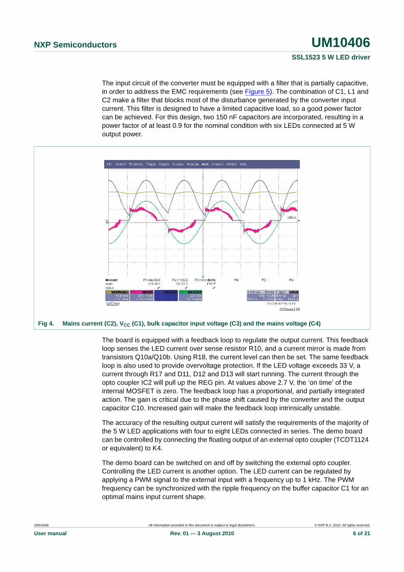
The input circuit of the converter must be equipped with a filter that is partially capacitive, in order to address the EMC requirements (see Figure 5). The combination of C1, L1 and C2 make a filter that blocks most of the disturbance generated by the converter input current. This filter is designed to have a limited capacitive load, so a good power factor can be achieved. For this design, two 150 nF capacitors are incorporated, resulting in a power factor of at least 0.9 for the nominal condition with six LEDs connected at 5 W output power.
The board is equipped with a feedback loop to regulate the output current. This feedback loop senses the LED current over sense resistor R10, and a current mirror is made from transistors Q10a/Q10b. Using R18, the current level can then be set. The same feedback loop is also used to provide overvoltage protection. If the LED voltage exceeds 33 V, a current through R17 and D11, D12 and D13 will start running. The current through the opto coupler IC2 will pull up the REG pin. At values above 2.7 V, the ‘on time’ of the internal MOSFET is zero. The feedback loop has a proportional, and partially integrated action. The gain is critical due to the phase shift caused by the converter and the output capacitor C10. Increased gain will make the feedback loop intrinsically unstable.
The accuracy of the resulting output current will satisfy the requirements of the majority of the 5 W LED applications with four to eight LEDs connected in series. The demo board can be controlled by connecting the floating output of an external opto coupler (TCDT1124 or equivalent) to K4.
The demo board can be switched on and off by switching the external opto coupler. Controlling the LED current is another option. The LED current can be regulated by applying a PWM signal to the external input with a frequency up to 1 kHz. The PWM frequency can be synchronized with the ripple frequency on the buffer capacitor C1 for an optimal mains input current shape.
Fig 4. Mains current (C2), VCC (C1), bulk capacitor input voltage (C3) and the mains voltage (C4)
019aaa135
UM10406 All information provided in this document is subject to legal disclaimers. © NXP B.V. 2010. All rights reserved.
User manual Rev. 01 — 3 August 2010 6 of 21

NXP Semiconductors UM10406SSL1523 5 W LED driver
6. Board system optimization
To meet specific customer application requirements, the modifications described in the following sections are possible.
6.1 Changing the output current and LED currentOne of the major advantages of a flyback converter over other topologies, is its suitability for driving LED configurations with a broad range of voltages. Essentially, changing the winding ratio whilst maintaining the value of the primary inductance, will shift the output working voltage accordingly. Part of the efficiency of the driver is linked to the output voltage. A lower output voltage will require increased transformation ratio, and will cause higher secondary losses. In practice, a mains operated flyback converter will have an efficiency > 80 % for high output voltages (like 40 V) down to 50 % for very low output voltages < 3 V. At low voltages, synchronous rectification becomes advisable to reduce rectification losses.
The NXP TEA 1761/TEA1762 can be used for this purpose, see Ref. 1. For exact calculations of transformer properties and peak current, refer to Ref. 2 application note AN10754, “How to design an LED driver using the SSL2101”, see Ref. 2.
6.2 Changing the output ripple currentThe output ripple current is mostly determined by the LED voltage, the LED dynamic resistance and the output capacitor. The present value of C10 has been chosen to optimize the capacitor size under typical load. The resulting ripple of ± 30 % will result in an expected deterioration of light output < 1 %.
The size for the buffer capacitor (C10) can be estimated from Equation 1:
(1)
Using a series of LEDs, the dynamic resistance of each LED can be multiplied by the number of LEDs. The current sense resistor (R10) should also be included in this calculation.
Example: For a ripple current of ± 30 %, and a mains frequency of 50 Hz, and a total dynamic resistance of 7 Ω, the resulting capacitance value will be 3.3333 / (314*7) = 1500 μF. The capacitor must be specified for the HF switching related ripple current of about 0.35 times the average effective LED current (ILED(AV)). For high lifetime applications, the ripple current specification of the electrolytic capacitor must be increased. For details, please contact the capacitor supplier.
6.3 Changing the load curveThe current load curve can be divided into the following two regions:
• Where the current control loop regulates the output current, the constant current output
• Where the IC limits the peak input current of the converter, the constant power output
C10I
ΔI------ 1
2πfnet Rdynamic⋅----------------------------------------⋅=
UM10406 All information provided in this document is subject to legal disclaimers. © NXP B.V. 2010. All rights reserved.
User manual Rev. 01 — 3 August 2010 7 of 21

NXP Semiconductors UM10406SSL1523 5 W LED driver
The constant power output occurs at output voltages above 23 V combined with an output power exceeding 5 W, see also Section 9, Figure 9. In this area, constant output power becomes the dominant control mechanism. At very low output voltages, the feedback loop will become non-functional, resulting again in constant output power mode. An output short-circuit will cause an output current of about 1 A, resulting in increased stress on the transformer TX1, shunt resistor R10, the output diode D10, and the snubber diode D3.
UM10406 All information provided in this document is subject to legal disclaimers. © NXP B.V. 2010. All rights reserved.
User manual Rev. 01 — 3 August 2010 8 of 21

xxxxxxxxxxxxxxxxxxxxx xxxxxxxxxxxxxxxxxxxxxxxxxx xxxxxxx x x x xxxxxxxxxxxxxxxxxxxxxxxxxxxxxx xxxxxxxxxxxxxxxxxxx xx xx xxxxx xxxxxxxxxxxxxxxxxxxxxxxxxxx xxxxxxxxxxxxxxxxxxx xxxxxx xxxxxxxxxxxxxxxxxxxxxxxxxxxxxxxxxxx xxxxxxxxxxxx x x xxxxxxxxxxxxxxxxxxxxx xxxxxxxxxxxxxxxxxxxxxxxxxxxxxx xxxxx xxxxxxxxxxxxxxxxxxxxxxxxxxxxxxxxxxxxxxxxxxxxxxxxxx xxxxxxxx xxxxxxxxxxxxxxxxxxxxxxxxx xxxxxxxxxxxxxxxxxxxx xxx
UM
10406
User m
anual
NXP Sem
iconductorsU
M10406
SSL1523 5 W LED
driver
7. Board schematic
019aaa136
R10
C12
1 μF, 35 V
R11220 Ω
R12220 Ω
R131 kΩ
R1410 kΩΩ
R1910 kΩ
D11BZV55-C22
Q10BCM857DS,115
D12148W-V-GS08
1 Ω, 1 W
K3-1
K3-2
K3-3
K3-4
K3-5
K3-6
1
2
K2
12 V(DC)to
25 V(DC)
A0
All information provided in this docum
ent is subject to legal disclaimers.
© N
XP B.V. 2010. All rights reserved.
Rev. 01 —
3 August 2010
9 of 21 Fig 5. Demo board schematic
SSL152X
DRAIN
HGND
HGND HGND HGND HGND
HGND
SGND
SGND
23
1
C15 Y-Type
D10
TX1760871038-E13
3 7
62
1
4
L10
R1510 k
R20
10 kΩ
R6
47 kΩ
R2
100 Ω
R1
33 Ω, 2 W
F1
FUSETIME-LAG, 1A
31
4
2
L11 mH
13R105C
D5
D4HER107
D2P6KE400A
D1RMB6S
C2150 nF400 V
C1150 nF400 V D3
P6KE200A
HER107
R184.7 kΩ
R17
1 kΩ
C136.8 μF
R166.2 kΩ
Q11BC857
1N4
D13BZV55-C6v2
IC2TCDT1124
10 μH, 2.674477210
C111 μF35 V
C101500 μF35 V
R92.4 Ω
R520 kΩ
C31 μF35 V
D6BZV55-C30
R4220 kΩ
C4330 pF
R36.8 kΩ R8
2.4 Ω
R7120 kΩ
SB1H100
1 nF, 250 V AC
VCC1
2
3
4
8
7
6
5
IC1
GND
RC
REG
n.c.
8RC
AUX
1
2
K4
CONTROL INPUT
2
1
K1
120 V(AC)to
230 V(AC)
+
−

NXP Semiconductors UM10406SSL1523 5 W LED driver
7.1 Bill of materials (BOM)
Table 2. Bill of materialsPart no.
Description Value PCB footprint Supplier Art no. Manufacturer Manufacturer part no.
C1 capacitor 150 nF 400 V - Farnell 9752838 - B32562J6154K
C2 capacitor 150 nF 400 V - Farnell 9752838 - B32562J6154K
C3 capacitor 1 μF 35 V 0603 Farnell 1611920 - GMK107BJ105KA-T
C11 capacitor 1 μF 35 V 0603 Farnell 1611920 - GMK107BJ105KA-T
C4 capacitor CPO NGO
330 pF 5 % 0603 - - - -
C10 capacitor low ESR
1500 μF 35 V pitch = 5 mm Farnell 1219477 Panasonic EEUFM1V152L
C12 capacitor low ESR
1 μF 35 V 0603 Farnell 1611920 - GMK107BJ105KA-T
C13 capacitor 6.8 μF 10 V 0805 Farnell 1572632 Kemet C0805C106K8PAC-TU
C15 Y-CAP Y-CAP 1 nF 250 V (AC)
- - 3531971 Murata DE1E3KX102MA5B
D1 diode bridge MB6S - - 1621770 Multicomp -
D2 TVS P6KE400A DO15 Farnell 1578842 - -
D3 TVS P6KE200A DO15 Farnell 1017750 Multicomp -
D4 diode fast HER107 DO41 Farnell 9565191 Multicomp -
D5 diode fast HER107 DO41 Farnell 9565191 Multicomp -
D6 Zener diode BZV55-C30 SOD80C Farnell 1081362RL NXP -
D10 diode Schottky SB1H100 DO41 Farnell 9550364 Vishay -
D11 Zener diode BZV55-C22 SOD80C Farnell 1097189 NXP -
D12 diode standard 1n4148 SMD Farnell 1469425 Vishay -
D13 Zener diode BZX384-B6V2 SOD-323 Farnell 1757832 NXP BZX384-B6V2
F1 fuse 1 A 250 V pitch = 5.08 mm Farnell 1637535 Schurter 34.6915
IC1 SSL1523 SSL1523 - - - NXP SSL1523
IC2 opto coupler CTR 160 320 % isolation = class II
TCDT1124 - Farnell 1045415 - -
K1 connector - pitch = 5.08 mm Farnell 1131853 Weidmuller PM5.08/2/90
K2 connector - pitch = 5.08 mm Farnell 1131853 Weidmuller PM5.08/2/90
K3 connector - pitch = 2.54 mm Farnell 1668357 Samtec SSW-106-02-G-S-RA
K4 connector - pitch = 5.08 mm Farnell 1131853 Weidmuller PM5.08/2/90
L1 coil 1 mH - 13R105C
pitch = 2 E Farnell 1710434 13R105C Murata
-
L10 coil 10 μH 2.6 A pitch = 5 mm - - Wuerth 744772100
UM10406 All information provided in this document is subject to legal disclaimers. © NXP B.V. 2010. All rights reserved.
User manual Rev. 01 — 3 August 2010 10 of 21

NXP Semiconductors UM10406SSL1523 5 W LED driver
8. Transformer specification
Figure 6 shows the transformer schematic:
Q10 dual transistor PNP
BCM857DS SC-74 (TSOP6) SOT457
Farnell 1757904 NXP BCM857DS
Q11 transistor PNP BC857 SMD - - - -
R1 resistor 33 Ω 2 W - Farnell 1565460 Welwyn -
R2 resistor 100 Ω 0603 - - - -
R3 resistor 6.8 kΩ 0603 - - - MC34751
R4 resistor 220 kΩ 0603 - - - -
R5 resistor 20 kΩ 0603 - - - -
R6 resistor 47 kΩ 0603 - - - -
R7 resistor 120 kΩ 0805 - - - -
R8 resistor not wirewound
2.4 Ω 1206 - - - -
R9 resistor not wirewound
2.4 Ω 1206 - - - -
R10 current sense resistor not wirewound
1 Ω 1 W 1 % - Farnell 5383894 RCD Components
F1S 1R
R11 resistor 220 Ω 1 % 0603 - - - -
R12 resistor 220 Ω 1 % 0603 - - - -
R13 resistor 1 kΩ 0603 - - - -
R17 resistor 1 kΩ 1 % 0603 - - - -
R14 resistor 10 kΩ 1 % 0603 - - - -
R15 resistor 10 kΩ 1 % 0603 - - - -
R19 resistor 10 kΩ 0603 - - - -
R20 resistor 10 kΩ 0603 - - - -
R16 resistor 6.2 kΩ 1 % 0603 - - - -
R18 variable resistor 4.7 kΩ potentiometer leaded
Farnell 1227568 Tyco CB10MV472ME
TX1 transformer 760871038 EE13 Wuerth 760871038 Wuerth 760871038
Table 2. Bill of materials …continued
Fig 6. Transformer schematic
6
72
3
4
1
N1
N3
019aaa137
N2
UM10406 All information provided in this document is subject to legal disclaimers. © NXP B.V. 2010. All rights reserved.
User manual Rev. 01 — 3 August 2010 11 of 21

NXP Semiconductors UM10406SSL1523 5 W LED driver
8.1 Winding specification
8.2 Electrical characteristics
• Nominal frequency = 100 kHz• Vbreakdown N1, N2 = 4 kV and N3, N2 = 4 kV• Leakage inductance = 20 μH (short N2)
8.3 Core and bobbin
• Core: EE13/6/6 (3C90 or better)• Air gap in centre leg• Bobbin: for EE13/6/6 core; bobbin must be suitable for Class II isolation requirements.
8.4 Physical dimensions
Fig 7. Winding specification
Table 3. Winding specificationWinding Section RatioPrimary to secondary N1 : N2 1 : 0.173
Primary to auxiliary N1 : N3 1 : 0.204
tape019aaa138
N1 (2-3): AWG39
bobbin
1 mm on pin 1 - 4 side
N1 (2-3): AWG39
N2 (7-6): AWG26 TIW
N3 (1-4): AWG35
Table 4. InductanceSection InductanceN1 1.85 mH ± 5 %
N2 56 μH
N3 75 μH
Fig 8. Transformer dimensions
15 mm
18.5 mm15.75 mm019aaa139
UM10406 All information provided in this document is subject to legal disclaimers. © NXP B.V. 2010. All rights reserved.
User manual Rev. 01 — 3 August 2010 12 of 21

NXP Semiconductors UM10406SSL1523 5 W LED driver
9. Appendix
9.1 Load curves
(1) LED current = 250 mA.
(2) LED current = 200 mA.
(3) LED current = 150 mA.
Fig 9. 120 V (AC) load curve at VLED = 19.5 V
(1) LED current = 250 mA.
(2) LED current = 200 mA.
(3) LED current = 150 mA.
Fig 10. 230 V (AC) load curve at VLED = 19.5 V
(1)
(2)
(3)
019aaa140
LED voltage (V)12 28242016
175
225
275
LEDcurrent(mA)
125
019aaa141
LED voltage (V)12 28242016
175
225
275
LEDcurrent(mA)
125
(3)
(1)
(2)
UM10406 All information provided in this document is subject to legal disclaimers. © NXP B.V. 2010. All rights reserved.
User manual Rev. 01 — 3 August 2010 13 of 21

NXP Semiconductors UM10406SSL1523 5 W LED driver
9.2 Efficiency curves
(1) LED current = 250 mA.
(2) LED current = 200 mA.
(3) LED current = 150 mA.
Fig 11. 120 V (AC) efficiency curve
(1) LED current = 250 mA.
(2) LED current = 200 mA.
(3) LED current = 150 mA.
Fig 12. 230 V (AC) efficiency curve
019aaa142
LED voltage (V)12 28242016
0.76
0.80
0.84
η(%)
0.72
(1)
(2)
(3)
019aaa143
LED voltage (V)12 28242016
0.76
0.80
0.84
η(%)
0.72
(1)
(3)
(2)
UM10406 All information provided in this document is subject to legal disclaimers. © NXP B.V. 2010. All rights reserved.
User manual Rev. 01 — 3 August 2010 14 of 21

NXP Semiconductors UM10406SSL1523 5 W LED driver
9.3 Input voltage dependency
9.4 EMC requirements
(1) LED current set at 250 mA nominal with a load of six LEDs in series (19.5 V).
Fig 13. Input voltage versus output current
Umains (V)70 270230150 190110
019aaa144
250
248
252
254
lout(mA)
246
(1)
Fig 14. EMC measurements at a mains voltage of 120 V (AC)
NXP Semiconductors
1 PKMAXH
2 AVCLRWR
SGL
6DB
9 kHz 30 MHz
dB�VdB�V
MT 1 msRBW 9 kHz
PREAMP OFFAtt 10 dB04.Dec 09 17:52
100 kHz 1 MHz 10 MHz
0
10
20
30
40
50
60
70
80
90
100
1
Marker 1 [T2 ] 48.64 dB�V 9.000000000 kHz
FCC15AVQ
FCC15BVQ
019aaa145
UM10406 All information provided in this document is subject to legal disclaimers. © NXP B.V. 2010. All rights reserved.
User manual Rev. 01 — 3 August 2010 15 of 21

NXP Semiconductors UM10406SSL1523 5 W LED driver
9.5 Mains conducted harmonics
Fig 15. EMC measurements at a mains voltage of 230 V (AC)
NXP Semiconductors
1 PKMAXH
2 AVCLRWR
SGL
6DB
9 kHz 30 MHz
dB�VdB�V
MT 1 msRBW 9 kHz
PREAMP OFFAtt 10 dB04.Dec 09 16:48
100 kHz 1 MHz 10 MHz
0
10
20
3
40
50
60
70
80
90
100LIMIT CHECK PASS
1
Marker 1 [T2 ] 50.66 dB�V 9.000000000 kHz
EN55015A
EN55015Q
019aaa146
Table 5. Mains conducted harmonicsHarmonic 230 V (AC) @ 50 Hz amplitude 120 V (AC) @ 60 Hz amplitude1 100 100
2 0 0
3 11.0 8.1
4 0 0
5 12.5 14
6 0 0
7 11.7 2.7
8 0 0
9 7.7 1.2
10 0 0
11 5.0 2.1
12 0 0
13 7.4 2.4
14 0 00
15 3.0 2.4
16 0 0
17 7.6 1.5
UM10406 All information provided in this document is subject to legal disclaimers. © NXP B.V. 2010. All rights reserved.
User manual Rev. 01 — 3 August 2010 16 of 21

NXP Semiconductors UM10406SSL1523 5 W LED driver
10. References
[1] TEA1761/TEA1762 — NXP GreenChip controllersfor synchronous rectification.
[2] AN10754 — How to design an LED driver using the SSL2101 or SSL2102.
[3] SSL152x — Datasheet - SMPS ICs for mains LED drivers.
18 0 0
19 1.1 3.4
20 0 0
Table 6. Total Harmonic Distortion and Power FactorParameter 230 V (AC) @ 50 Hz amplitude 120 V (AC) @ 50 Hz amplitudeTHD 27.1 21.6
Power Factor (PF) 0.90 0.98
Table 5. Mains conducted harmonics …continued
Harmonic 230 V (AC) @ 50 Hz amplitude 120 V (AC) @ 60 Hz amplitude
UM10406 All information provided in this document is subject to legal disclaimers. © NXP B.V. 2010. All rights reserved.
User manual Rev. 01 — 3 August 2010 17 of 21

NXP Semiconductors UM10406SSL1523 5 W LED driver
11. Legal information
11.1 DefinitionsDraft — The document is a draft version only. The content is still under internal review and subject to formal approval, which may result in modifications or additions. NXP Semiconductors does not give any representations or warranties as to the accuracy or completeness of information included herein and shall have no liability for the consequences of use of such information.
11.2 DisclaimersLimited warranty and liability — Information in this document is believed to be accurate and reliable. However, NXP Semiconductors does not give any representations or warranties, expressed or implied, as to the accuracy or completeness of such information and shall have no liability for the consequences of use of such information.
In no event shall NXP Semiconductors be liable for any indirect, incidental, punitive, special or consequential damages (including - without limitation - lost profits, lost savings, business interruption, costs related to the removal or replacement of any products or rework charges) whether or not such damages are based on tort (including negligence), warranty, breach of contract or any other legal theory.
Notwithstanding any damages that customer might incur for any reason whatsoever, NXP Semiconductors’ aggregate and cumulative liability towards customer for the products described herein shall be limited in accordance with the Terms and conditions of commercial sale of NXP Semiconductors.
Right to make changes — NXP Semiconductors reserves the right to make changes to information published in this document, including without limitation specifications and product descriptions, at any time and without notice. This document supersedes and replaces all information supplied prior to the publication hereof.
Suitability for use — NXP Semiconductors products are not designed, authorized or warranted to be suitable for use in life support, life-critical or safety-critical systems or equipment, nor in applications where failure or malfunction of an NXP Semiconductors product can reasonably be expected to result in personal injury, death or severe property or environmental damage. NXP Semiconductors accepts no liability for inclusion and/or use of NXP Semiconductors products in such equipment or applications and therefore such inclusion and/or use is at the customer’s own risk.
Applications — Applications that are described herein for any of these products are for illustrative purposes only. NXP Semiconductors makes no representation or warranty that such applications will be suitable for the specified use without further testing or modification.
Customers are responsible for the design and operation of their applications and products using NXP Semiconductors products, and NXP Semiconductors accepts no liability for any assistance with applications or customer product
design. It is customer’s sole responsibility to determine whether the NXP Semiconductors product is suitable and fit for the customer’s applications and products planned, as well as for the planned application and use of customer’s third party customer(s). Customers should provide appropriate design and operating safeguards to minimize the risks associated with their applications and products.
NXP Semiconductors does not accept any liability related to any default, damage, costs or problem which is based on any weakness or default in the customer’s applications or products, or the application or use by customer’s third party customer(s). Customer is responsible for doing all necessary testing for the customer’s applications and products using NXP Semiconductors products in order to avoid a default of the applications and the products or of the application or use by customer’s third party customer(s). NXP does not accept any liability in this respect.
Export control — This document as well as the item(s) described herein may be subject to export control regulations. Export might require a prior authorization from national authorities.
Evaluation products — This product is provided on an “as is” and “with all faults” basis for evaluation purposes only. NXP Semiconductors, its affiliates and their suppliers expressly disclaim all warranties, whether express, implied or statutory, including but not limited to the implied warranties of non-infringement, merchantability and fitness for a particular purpose. The entire risk as to the quality, or arising out of the use or performance, of this product remains with customer.
In no event shall NXP Semiconductors, its affiliates or their suppliers be liable to customer for any special, indirect, consequential, punitive or incidental damages (including without limitation damages for loss of business, business interruption, loss of use, loss of data or information, and the like) arising out the use of or inability to use the product, whether or not based on tort (including negligence), strict liability, breach of contract, breach of warranty or any other theory, even if advised of the possibility of such damages.
Notwithstanding any damages that customer might incur for any reason whatsoever (including without limitation, all damages referenced above and all direct or general damages), the entire liability of NXP Semiconductors, its affiliates and their suppliers and customer’s exclusive remedy for all of the foregoing shall be limited to actual damages incurred by customer based on reasonable reliance up to the greater of the amount actually paid by customer for the product or five dollars (US$5.00). The foregoing limitations, exclusions and disclaimers shall apply to the maximum extent permitted by applicable law, even if any remedy fails of its essential purpose.
11.3 TrademarksNotice: All referenced brands, product names, service names and trademarks are the property of their respective owners.
UM10406 All information provided in this document is subject to legal disclaimers. © NXP B.V. 2010. All rights reserved.
User manual Rev. 01 — 3 August 2010 18 of 21
NXP Semiconductors UM10406SSL1523 5 W LED driver
12. Tables
Table 1. Specification . . . . . . . . . . . . . . . . . . . . . . . . . . .3Table 2. Bill of materials . . . . . . . . . . . . . . . . . . . . . . . .10Table 3. Winding specification . . . . . . . . . . . . . . . . . . . .12Table 4. Inductance . . . . . . . . . . . . . . . . . . . . . . . . . . . .12Table 5. Mains conducted harmonics . . . . . . . . . . . . . .16Table 6. Total Harmonic Distortion and Power Factor . .17
UM10406 All information provided in this document is subject to legal disclaimers. © NXP B.V. 2010. All rights reserved.
User manual Rev. 01 — 3 August 2010 19 of 21
continued >>

NXP Semiconductors UM10406SSL1523 5 W LED driver
13. Figures
Fig 1. Demo board top . . . . . . . . . . . . . . . . . . . . . . . . . . .4Fig 2. Demo board bottom . . . . . . . . . . . . . . . . . . . . . . . .4Fig 3. Demo board connection diagram. . . . . . . . . . . . . .5Fig 4. Mains current (C2), VCC (C1), bulk capacitor
input voltage (C3) and the mains voltage (C4) . . .6Fig 5. Demo board schematic . . . . . . . . . . . . . . . . . . . . .9Fig 6. Transformer schematic . . . . . . . . . . . . . . . . . . . . 11Fig 7. Winding specification . . . . . . . . . . . . . . . . . . . . . .12Fig 8. Transformer dimensions . . . . . . . . . . . . . . . . . . .12Fig 9. 120 V (AC) load curve at VLED = 19.5 V . . . . . . .13Fig 10. 230 V (AC) load curve at VLED = 19.5 V . . . . . . .13Fig 11. 120 V (AC) efficiency curve . . . . . . . . . . . . . . . . .14Fig 12. 230 V (AC) efficiency curve . . . . . . . . . . . . . . . . .14Fig 13. Input voltage versus output current . . . . . . . . . . .15Fig 14. EMC measurements at a mains voltage
of 120 V (AC) . . . . . . . . . . . . . . . . . . . . . . . . . . . .15Fig 15. EMC measurements at a mains voltage
of 230 V (AC) . . . . . . . . . . . . . . . . . . . . . . . . . . . .16
UM10406 All information provided in this document is subject to legal disclaimers. © NXP B.V. 2010. All rights reserved.
User manual Rev. 01 — 3 August 2010 20 of 21
continued >>

NXP Semiconductors UM10406SSL1523 5 W LED driver
14. Contents
1 Introduction . . . . . . . . . . . . . . . . . . . . . . . . . . . . 31.1 General description . . . . . . . . . . . . . . . . . . . . . 32 Specification. . . . . . . . . . . . . . . . . . . . . . . . . . . . 33 Demo board views . . . . . . . . . . . . . . . . . . . . . . . 44 Demo board connections . . . . . . . . . . . . . . . . . 54.1 Connecting the demo board: . . . . . . . . . . . . . . 55 Functional description . . . . . . . . . . . . . . . . . . . 56 Board system optimization. . . . . . . . . . . . . . . . 76.1 Changing the output current and LED current . 76.2 Changing the output ripple current . . . . . . . . . . 76.3 Changing the load curve. . . . . . . . . . . . . . . . . . 77 Board schematic . . . . . . . . . . . . . . . . . . . . . . . . 97.1 Bill of materials (BOM) . . . . . . . . . . . . . . . . . . 108 Transformer specification. . . . . . . . . . . . . . . . 118.1 Winding specification . . . . . . . . . . . . . . . . . . . 128.2 Electrical characteristics . . . . . . . . . . . . . . . . . 128.3 Core and bobbin . . . . . . . . . . . . . . . . . . . . . . . 128.4 Physical dimensions . . . . . . . . . . . . . . . . . . . . 129 Appendix . . . . . . . . . . . . . . . . . . . . . . . . . . . . . 139.1 Load curves . . . . . . . . . . . . . . . . . . . . . . . . . . 139.2 Efficiency curves. . . . . . . . . . . . . . . . . . . . . . . 149.3 Input voltage dependency. . . . . . . . . . . . . . . . 159.4 EMC requirements . . . . . . . . . . . . . . . . . . . . . 159.5 Mains conducted harmonics. . . . . . . . . . . . . . 1610 References . . . . . . . . . . . . . . . . . . . . . . . . . . . . 1711 Legal information. . . . . . . . . . . . . . . . . . . . . . . 1811.1 Definitions. . . . . . . . . . . . . . . . . . . . . . . . . . . . 1811.2 Disclaimers . . . . . . . . . . . . . . . . . . . . . . . . . . . 1811.3 Trademarks. . . . . . . . . . . . . . . . . . . . . . . . . . . 1812 Tables . . . . . . . . . . . . . . . . . . . . . . . . . . . . . . . . 1913 Figures . . . . . . . . . . . . . . . . . . . . . . . . . . . . . . . 2014 Contents . . . . . . . . . . . . . . . . . . . . . . . . . . . . . . 21
© NXP B.V. 2010. All rights reserved.For more information, please visit: http://www.nxp.comFor sales office addresses, please send an email to: [email protected]
Date of release: 3 August 2010Document identifier: UM10406
Please be aware that important notices concerning this document and the product(s)described herein, have been included in section ‘Legal information’.