Embed Size (px)
Citation preview
UM10359UBA2016AT HFTL demo board with boost and dimmingRev. 1.1 — 1 July 2011 User manual
Document information
Info Content
Keywords UBA2016AT, ballast, 28 W 2D lamp, dimming, boost
Abstract This User manual describes a demonstration (demo) board using the UBA2016AT controller for driving a 28 W fluorescent lamp.
NXP Semiconductors UM10359UBA2016AT HFTL demo board with boost and dimming
Revision history
Rev Date Description
v.1.1 20110701 second version
v.1 20110303 first version
UM10359 All information provided in this document is subject to legal disclaimers. © NXP B.V. 2011. All rights reserved.
User manual Rev. 1 — 1 July 2011 2 of 18
Contact informationFor more information, please visit: http://www.nxp.com
For sales office addresses, please send an email to: [email protected]
NXP Semiconductors UM10359UBA2016AT HFTL demo board with boost and dimming
1. Introduction
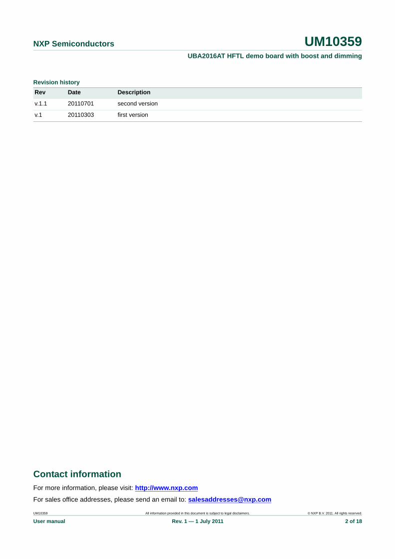
This User manual describes a demonstration (demo) board with boost and dimming functionality using the UBA2016AT controller. The demo board drives a 28 W 2D (square) fluorescent lamp.
Fig 1. UBA2016AT demo board
019aaa577
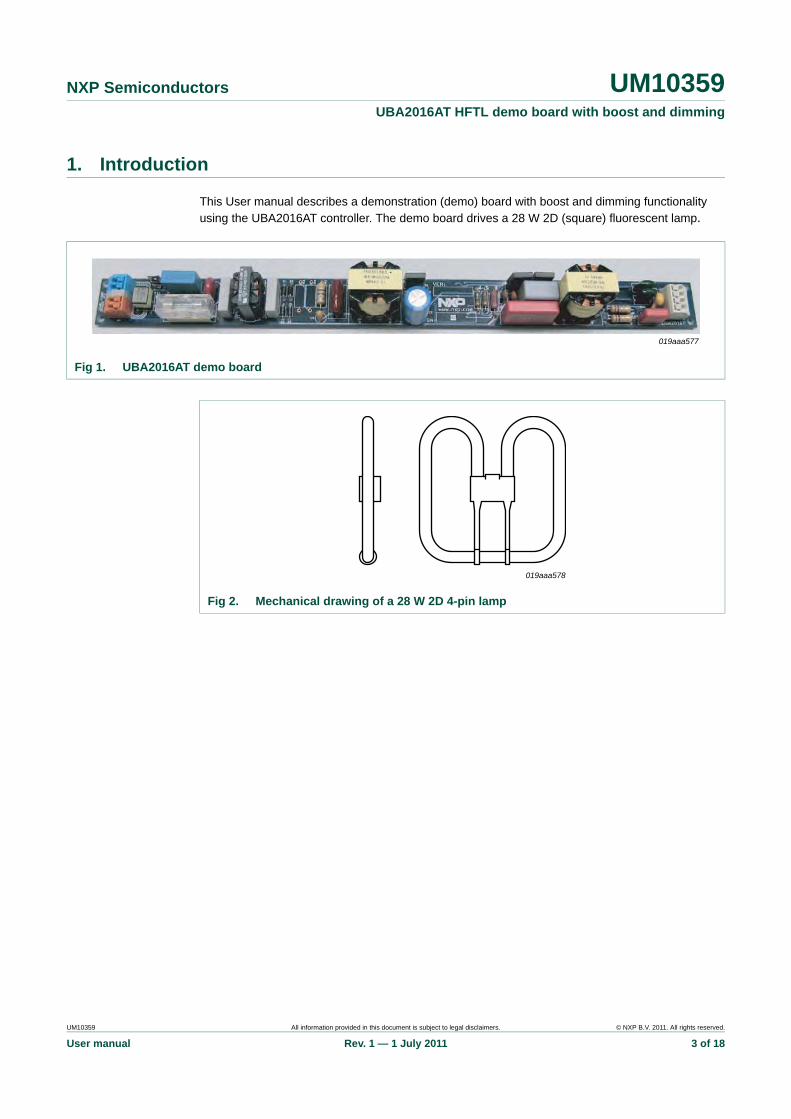
Fig 2. Mechanical drawing of a 28 W 2D 4-pin lamp
019aaa578
UM10359 All information provided in this document is subject to legal disclaimers. © NXP B.V. 2011. All rights reserved.
User manual Rev. 1 — 1 July 2011 3 of 18
NXP Semiconductors UM10359UBA2016AT HFTL demo board with boost and dimming
2. Safety warning
The demo board is powered by AC mains voltage. Avoid touching the board when power is applied. An isolated housing is obligatory when used in uncontrolled, non-laboratory environments.
3. Specification
WARNING
Lethal voltage and fire ignition hazard
The non-insulated high voltages that are present when operating this product, constitute a risk of electric shock, personal injury, death and/or ignition of fire.
This product is intended for evaluation purposes only. It shall be operated in a designated test area by personnel qualified according to local requirements and labor laws to work with non-insulated mains voltages and high-voltage circuits. This product shall never be operated unattended.
Table 1. Demo board specification
Description Value/Comment
Ballast type electronic
Starting method programmed start with pre-heat
Number of lamp terminals 4
Line voltage 220 V to 240 V AC
Line frequency 50/60 Hz
Number of lamps 1
Dimming interface 1 V to 10 V
Transient protection complies with IEC 61547
Table 2. Lamps supported
Lamp type Description
SQE28835 4 pins OSRAM square CFL 28 W
Table 3. Ballast performance
Lamp type Number of lamps
Rated lamp power (W)
Maximum THD
Maximum lamp current crest factor
Power factor Nominal lamp current (mA)
Minimal lamp current (mA)
SQE28835
(OSRAM)
1 28 10 % 1.7 >0.95 300 5.0
UM10359 All information provided in this document is subject to legal disclaimers. © NXP B.V. 2011. All rights reserved.
User manual Rev. 1 — 1 July 2011 4 of 18
NXP Semiconductors UM10359UBA2016AT HFTL demo board with boost and dimming
4. Board description
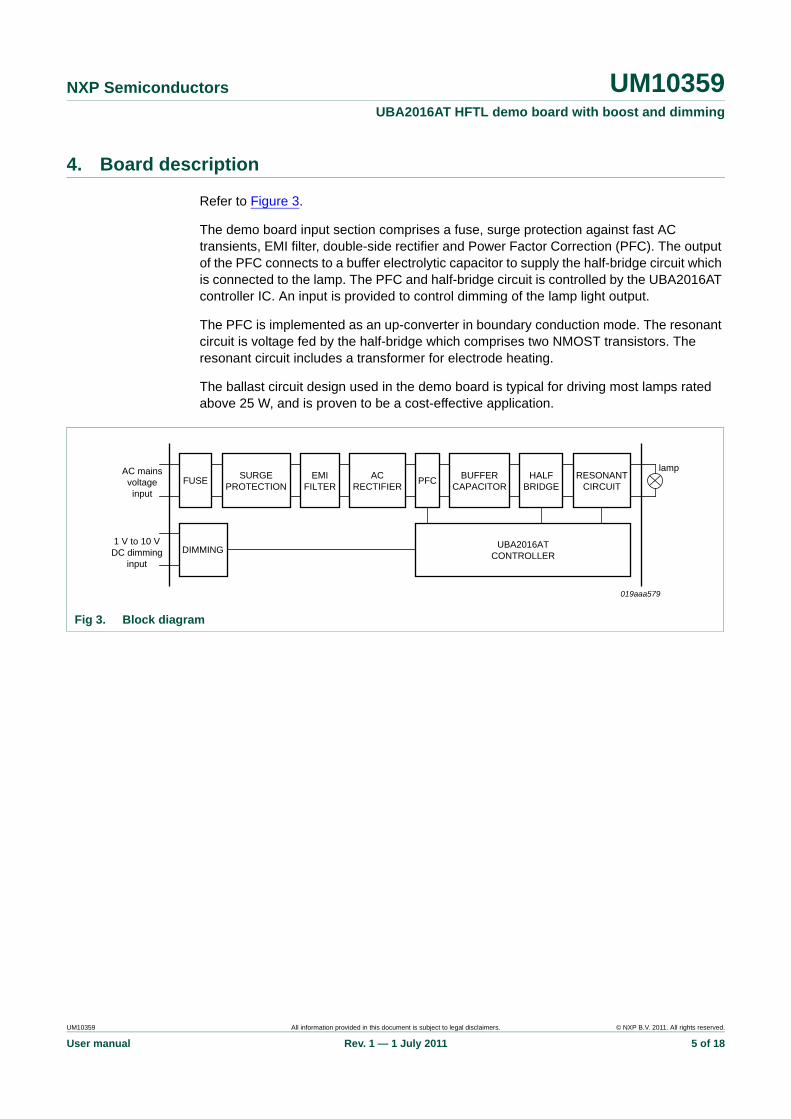
Refer to Figure 3.
The demo board input section comprises a fuse, surge protection against fast AC transients, EMI filter, double-side rectifier and Power Factor Correction (PFC). The output of the PFC connects to a buffer electrolytic capacitor to supply the half-bridge circuit which is connected to the lamp. The PFC and half-bridge circuit is controlled by the UBA2016AT controller IC. An input is provided to control dimming of the lamp light output.
The PFC is implemented as an up-converter in boundary conduction mode. The resonant circuit is voltage fed by the half-bridge which comprises two NMOST transistors. The resonant circuit includes a transformer for electrode heating.
The ballast circuit design used in the demo board is typical for driving most lamps rated above 25 W, and is proven to be a cost-effective application.
Fig 3. Block diagram
019aaa579
SURGEPROTECTION
ACRECTIFIER
BUFFERCAPACITOR
RESONANTCIRCUIT
UBA2016ATCONTROLLER
DIMMING1 V to 10 VDC dimming
input
AC mainsvoltageinput
FUSE PFClamp
EMIFILTER
HALFBRIDGE
UM10359 All information provided in this document is subject to legal disclaimers. © NXP B.V. 2011. All rights reserved.
User manual Rev. 1 — 1 July 2011 5 of 18
NXP Semiconductors UM10359UBA2016AT HFTL demo board with boost and dimming
4.1 Performance indicators
4.1.1 Efficiency, power factor and THD
4.1.1.1 Dimming curve
4.1.1.2 Lamp current boost at startup
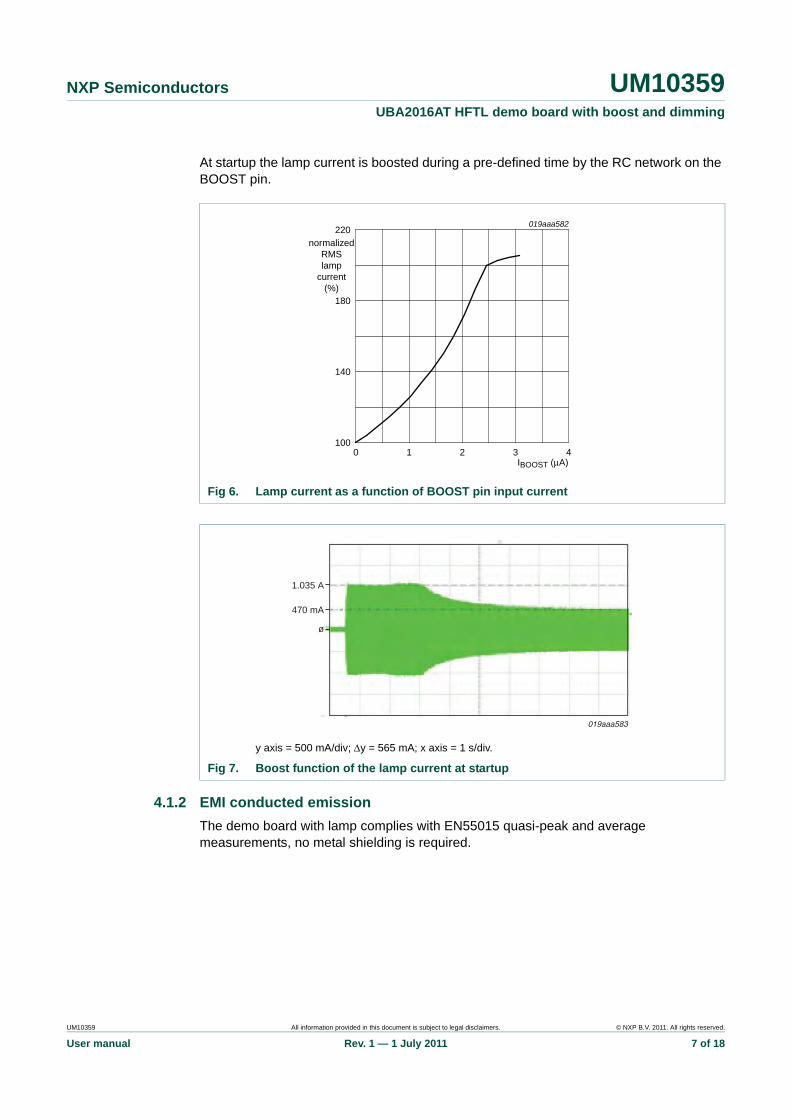
A boost function is implemented to enable reduced lamp run-up times. This is needed typically for outdoor applications or for amalgam lamps.
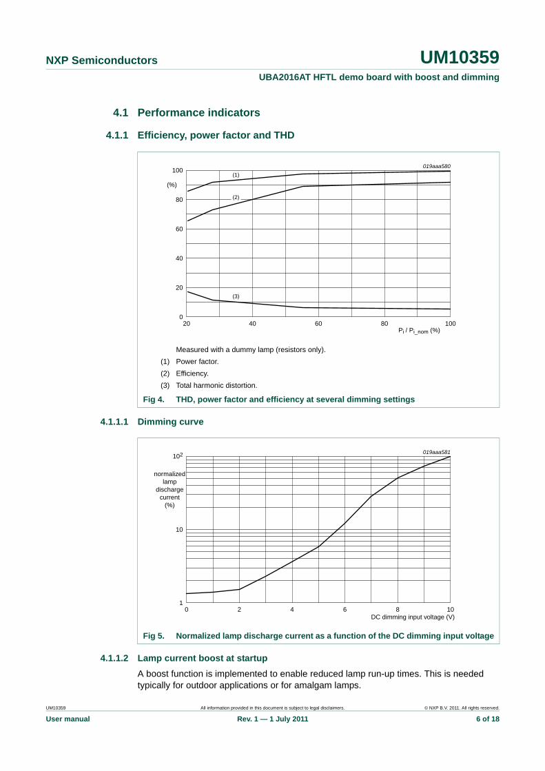
Measured with a dummy lamp (resistors only).
(1) Power factor.
(2) Efficiency.
(3) Total harmonic distortion.
Fig 4. THD, power factor and efficiency at several dimming settings
Pi / Pi_nom (%)20 100806040
019aaa580
40
60
20
80
100
(%)
0
(1)
(2)
(3)
Fig 5. Normalized lamp discharge current as a function of the DC dimming input voltage
019aaa581
10
102
normalizedlamp
dischargecurrent
(%)
1
DC dimming input voltage (V)0 1084 62
UM10359 All information provided in this document is subject to legal disclaimers. © NXP B.V. 2011. All rights reserved.
User manual Rev. 1 — 1 July 2011 6 of 18
NXP Semiconductors UM10359UBA2016AT HFTL demo board with boost and dimming
At startup the lamp current is boosted during a pre-defined time by the RC network on the BOOST pin.
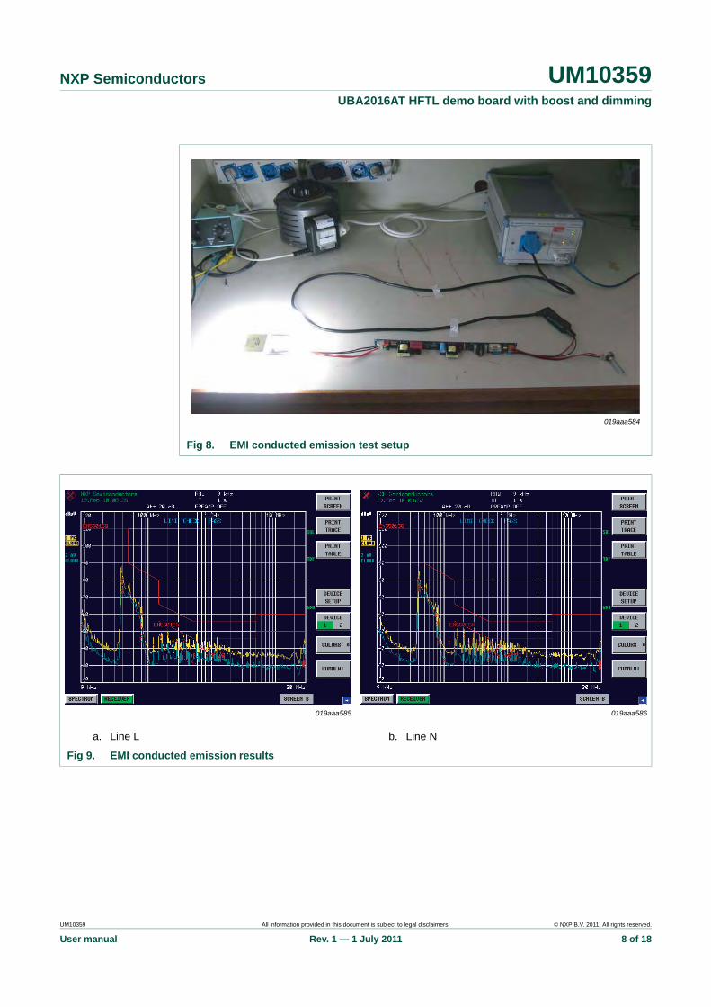
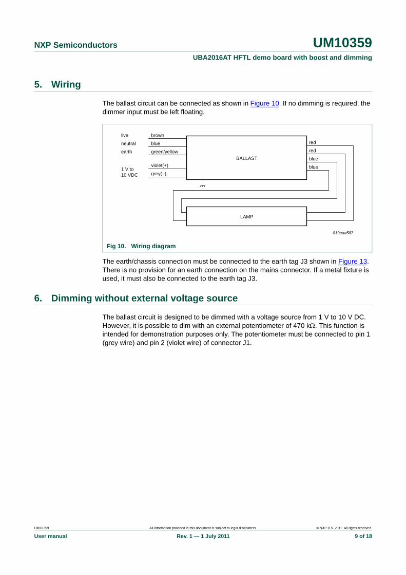
4.1.2 EMI conducted emission
The demo board with lamp complies with EN55015 quasi-peak and average measurements, no metal shielding is required.
Fig 6. Lamp current as a function of BOOST pin input current
y axis = 500 mA/div; y = 565 mA; x axis = 1 s/div.
Fig 7. Boost function of the lamp current at startup
IBOOST (μA)0 431 2
019aaa582
140
180
220normalized
RMSlamp
current(%)
100
1.035 A
470 mA
ø
UM10359 All information provided in this document is subject to legal disclaimers. © NXP B.V. 2011. All rights reserved.
User manual Rev. 1 — 1 July 2011 7 of 18
NXP Semiconductors UM10359UBA2016AT HFTL demo board with boost and dimming
Fig 8. EMI conducted emission test setup
019aaa584
a. Line L b. Line N
Fig 9. EMI conducted emission results
019aaa585 019aaa586
UM10359 All information provided in this document is subject to legal disclaimers. © NXP B.V. 2011. All rights reserved.
User manual Rev. 1 — 1 July 2011 8 of 18
NXP Semiconductors UM10359UBA2016AT HFTL demo board with boost and dimming
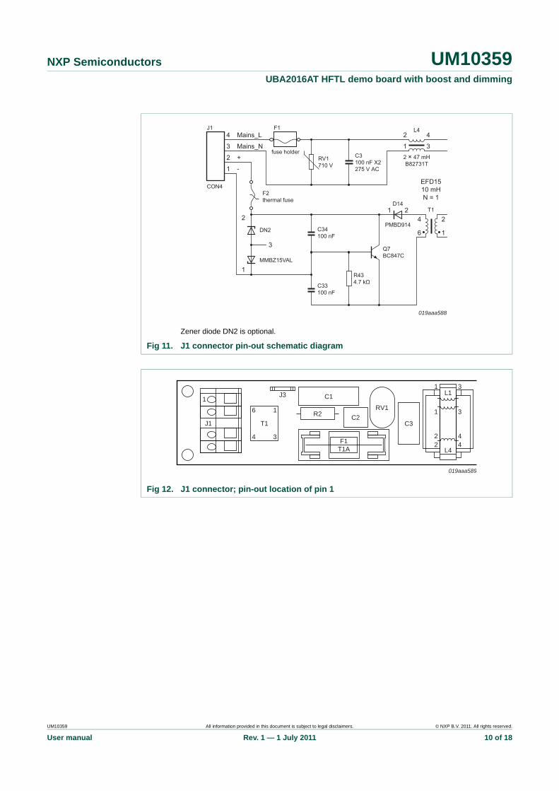
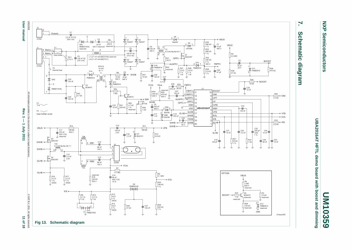
5. Wiring
The ballast circuit can be connected as shown in Figure 10. If no dimming is required, the dimmer input must be left floating.
The earth/chassis connection must be connected to the earth tag J3 shown in Figure 13. There is no provision for an earth connection on the mains connector. If a metal fixture is used, it must also be connected to the earth tag J3.
6. Dimming without external voltage source
The ballast circuit is designed to be dimmed with a voltage source from 1 V to 10 V DC. However, it is possible to dim with an external potentiometer of 470 k. This function is intended for demonstration purposes only. The potentiometer must be connected to pin 1 (grey wire) and pin 2 (violet wire) of connector J1.
Fig 10. Wiring diagram
019aaa587
BALLAST
LAMP
brown
blue
green/yellow
live
neutral
1 V to10 VDC
earth
violet(+)
grey(−)
red
red
blue
blue
UM10359 All information provided in this document is subject to legal disclaimers. © NXP B.V. 2011. All rights reserved.
User manual Rev. 1 — 1 July 2011 9 of 18
NXP Semiconductors UM10359UBA2016AT HFTL demo board with boost and dimming
Zener diode DN2 is optional.
Fig 11. J1 connector pin-out schematic diagram
Fig 12. J1 connector; pin-out location of pin 1
019aaa588
2 4
1 3C3100 nF X2275 V AC
RV1710 V
F1
F2thermal fuse
fuse holder
EFD1510 mHN = 1
4J1
CON4
3
2
1
Mains_L
Mains_N
+
-
DN2 C34100 nF
C33100 nF
Q7BC847C
1
2
6
41 2
PMBD914
D14
L4
2 × 47 mHB82731T
T1
R434.7 kΩ
3
2
1MMBZ15VAL
019aaa589
T1
J3 C1
1 3
1 3
2 42 4
L1
L4
RV1
C2C3
F1T1A
R26
1
J1
4
1
3
UM10359 All information provided in this document is subject to legal disclaimers. © NXP B.V. 2011. All rights reserved.
User manual Rev. 1 — 1 July 2011 10 of 18
xxxx xxxxxxxxxxxxxxxxxxxxxxxxxxxxxx x xxxxxxxxxxxxxx xxxxxxxxxx xxx xxxxxx xxxxxxxxxxxxxxxxxxxxxxx xxxxxxxxxxxxxxxxxxxxxx xxxxx xxxxxx xx xxxxxxxxxxxxxxxxxxxxxxxxxxxxx xxxxxxxxxxxxxxxxxxxxxx xxxxxxxxxxx xxxxxxx xxxxxxxxxxxxxxxxxxx xxxxxxxxxxxxxxxx xxxxxxxxxxxxxx xxxxxx xx xxxxxxxxxxxxxxxxxxxxxxxxxxxxxxxx xxxxxxxxxxxxxxxxxxxxxxxx xxxxxxx xxxxxxxxxxxxxxxxxxxxxxxxxxxxxxxxxxxxxxxxxxxxxx xxxxxxxxxxx xxxxx x x
UM
10359
User m
anu
al
NX
P S
emico
nd
ucto
7. S
chem
atic d
2 1
3R2C2
33 nFDN1 220 Ω
C1
2.2 nF X1/Y2250 V AC
Chassis
VBUS
BOOST
VBUSD11N4007
1
2
D31N4007
1
2
2J3
CON4
1
2D5
1
2D6
1N4007
1
R30390 kΩ
C5
C7
5.2 MW
2 4
1 3C3100 nF X2275 V AC
400 V reservedMMBZ15VALreserved
reserved
RV1710 V
F1
fuse holder
T25.0 mH Np:Ns=51:1
4J1
3
2
1
Mains_L
Mains_N
+
- D21N4007
1
2
D41N4007
Q12SK37671
2 1 D10
GPFC
C4
100 nF X2275 V AC
C6150 nF400 V
L1 (2 × 47 mH B82731M) reservedL4 (2 × 47 mH B82731T)
3
6
2
8
UF4006
R31100 Ω
1 %R32390 kΩ1 %
10 μF450 V
R34330 kΩ1 %
R2
rsU
M10359
UB
A2
016
AT
HF
TL
de
mo
bo
ard w
ith b
oo
st an
d d
imm
ing
iagram
019aaa590
Q4BC847Creserved
D11PMBD914
1
2
10 μF25 V
357 kΩ
R36470 kΩ
C3510 nF
C2682 nF
C2210 nF
R2133 kΩ1 %
R221 kΩ
C243.3 nF
C23
100 nF
C3010 nF
R19
VFB
EOL
IFB2.2 kΩ
R24DIM
3.3 kΩ
R26BOOST
10 kΩ
R37
1 Ωreserved
C25220 pFC0G1 %
VBUS
DIM
D12PMBD914reserved
2
1
R38100 kΩreserved
R375 kΩreserved
R41 MΩ500 Vreserved
All inform
ation provided
in this docum
ent is subject to leg
al disclaim
ers.©
NX
P B
.V. 2011. A
ll rights reserved.
Rev. 1 —
1 July 2011
11 of 18
Fig 13. Schematic diagram
D13PMBD914
C3210 nF
R41200 kΩ
R15
130 kΩ500 V
R11C15
C161.5 nF
R126.8 kΩ
D7BAS101
100 pF2 kV
100 kΩC11470 nF630 V DCreserved
R391 kΩ
R424.7 kΩ1 %reserved
DIM
F2thermal fuse
EFD1510 mHN = 1
CON4
4J4
CON4
3
2
1
DN2 C34100 nF
C33100 nF
Q7BC847C
Q6BC847C
Q5BFT46
1
2
2
1
D16PMBD914
Q32SK3767
C103.3 nF2 kV
2
PMBD914
1AUXPFC FBPFC
BOOST
2
6
41 2
PMBD914
SHHB
D14T1 R8
10 kΩ500 V
R40
1 MΩ
C9
10 pF500 V
R434.7 kΩ
3
2
1MMBZ15VAL
fuse holder cover
F3T1A
F4
U1
11FBPFC
FBPFC
10BOOST
UBA2016AT
12COMPFC
9DIM
13AUXPFC
AUXPFC 8CPT
14GPFC
GPFC 7CF
15GND
6CIFB
16VDD
5IREF
17GLHB
GLHB
23
3
1
4VFB
18SHHB
SHHB
SHHB
VCdc Vbus
C20
100 nF50 V
D8A
C171 nF
C12
T3B
56T3A2.5 mH Np:Ns=30:1:1
23
8
3
1
WB1
VBUS
GHHB
Q22SK3767
GLHB
SHHB
WB2
VCdc
EOL
IFB
1
3
2
7
T3C
68 nF100 V
C13
D9PMBD6100
68 nF100 V
R163.3 Ω1 %0W25
R173.3 Ω1 %0W25
C1468 nF400 V DC10 %
R1318 Ω1 %0W25
R102.7 Ω1 W
R92.7 Ω1 W
R1418 Ω1 %0W25
R46220 kΩ1 %
reservedR18330 kΩ500 V
R4527 kΩ
C31100 nF
R65.1 MW
R20180 kΩ1 %
R7
5.1 MΩ
C27100 nF
C29
C36100 nF
R4710 kΩ
R273.9 Ω1 %1 W
R283.9 Ω1 %1 W
R33reserved R29
3.3 kΩ1 %
C2847 pF
R4
200 V
470 nF
C37
4.7 nFR23
82 kΩ
C8330 pF500 V
reservedR25470 kΩ500 V
R44330 kΩ500 V
C18470 nFD8B
BAV99
BAV99
3EOL
C19100 pF
C2110 nF
OPTION
19FSHB
2IFB
20GHHB
GHHBVFB
1SLHB
SLHB
D15PMBD7000
SLHB
xxxx xxxxxxxxxxxxxxxxxxxxxxxxxxxxxx x xxxxxxxxxxxxxx xxxxxxxxxx xxx xxxxxx xxxxxxxxxxxxxxxxxxxxxxx xxxxxxxxxxxxxxxxxxxxxx xxxxx xxxxxx xx xxxxxxxxxxxxxxxxxxxxxxxxxxxxx xxxxxxxxxxxxxxxxxxxxxx xxxxxxxxxxx xxxxxxx xxxxxxxxxxxxxxxxxxx xxxxxxxxxxxxxxxx xxxxxxxxxxxxxx xxxxxx xx xxxxxxxxxxxxxxxxxxxxxxxxxxxxxxxx xxxxxxxxxxxxxxxxxxxxxxxx xxxxxxx xxxxxxxxxxxxxxxxxxxxxxxxxxxxxxxxxxxxxxxxxxxxxx xxxxxxxxxxx xxxxx x x
UM
10359
User m
anu
al
NX
P S
emico
nd
ucto
8. L
ayou
t
rsU
M10359
UB
A2
016
AT
HF
TL
de
mo
bo
ard w
ith b
oo
st an
d d
imm
ing
All inform
ation provided
in this docum
ent is subject to leg
al disclaim
ers.©
NX
P B
.V. 2011. A
ll rights reserved.
Rev. 1 —
1 July 2011
12 of 18
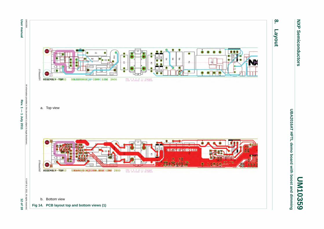
a. Top view
b. Bottom view
Fig 14. PCB layout top and bottom views (1)
xxxxxxxxxxxxxxxxxxxxx xxxxxxxxxxxxxxxxxxxxxxxxxx xxxxxxx x x x xxxxxxxxxxxxxxxxxxxxxxxxxxxxxx xxxxxxxxxxxxxxxxxxx xx xx xxxxx xxxxxxxxxxxxxxxxxxxxxxxxxxx xxxxxxxxxxxxxxxxxxx xxxxxx xxxxxxxxxxxxxxxxxxxxxxxxxxxxxxxxxxx xxxxxxxxxxxx x x xxxxxxxxxxxxxxxxxxxxx xxxxxxxxxxxxxxxxxxxxxxxxxxxxxx xxxxx xxxxxxxxxxxxxxxxxxxxxxxxxxxxxxxxxxxxxxxxxxxxxxxxxx xxxxxxxx xxxxxxxxxxxxxxxxxxxxxxxxx xxxxxxxxxxxxxxxxxxxx xxx
UM
10359
User m
anu
al
NX
P S
emico
nd
ucto
rsU
M10359
UB
A2
016
AT
HF
TL
de
mo
bo
ard w
ith b
oo
st an
d d
imm
ing
All inform
ation provided
in this docum
ent is subject to leg
al disclaim
ers.©
NX
P B
.V. 2011. A
ll rights reserved.
Rev. 1 —
1 July 2011
13 of 18
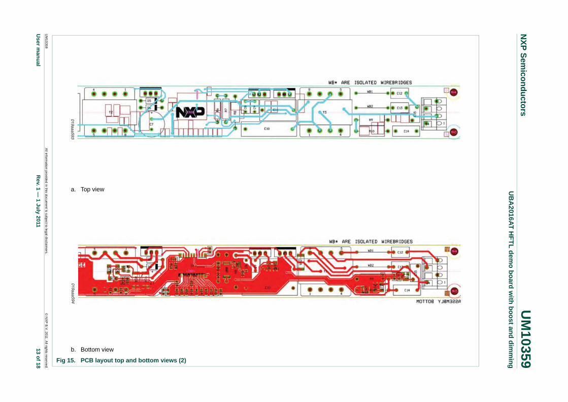
a. Top view
b. Bottom view
Fig 15. PCB layout top and bottom views (2)
NXP Semiconductors UM10359UBA2016AT HFTL demo board with boost and dimming
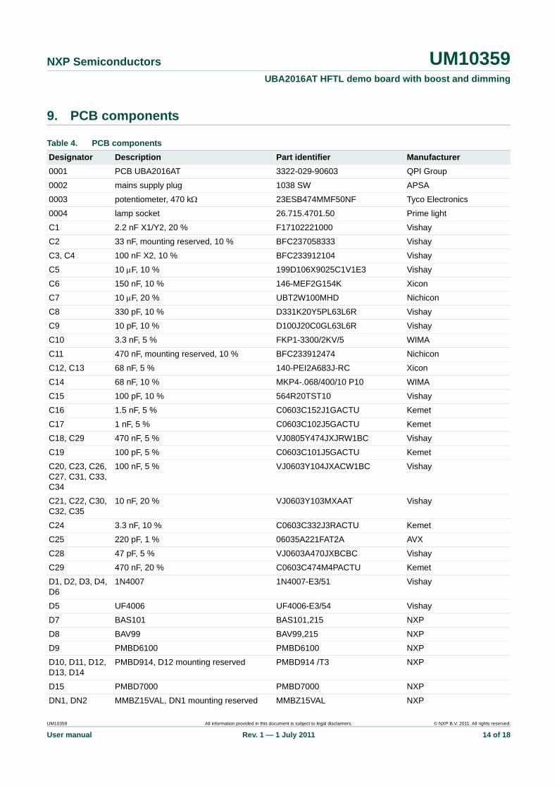
9. PCB components
Table 4. PCB components
Designator Description Part identifier Manufacturer
0001 PCB UBA2016AT 3322-029-90603 QPI Group
0002 mains supply plug 1038 SW APSA
0003 potentiometer, 470 k 23ESB474MMF50NF Tyco Electronics
0004 lamp socket 26.715.4701.50 Prime light
C1 2.2 nF X1/Y2, 20 % F17102221000 Vishay
C2 33 nF, mounting reserved, 10 % BFC237058333 Vishay
C3, C4 100 nF X2, 10 % BFC233912104 Vishay
C5 10 F, 10 % 199D106X9025C1V1E3 Vishay
C6 150 nF, 10 % 146-MEF2G154K Xicon
C7 10 F, 20 % UBT2W100MHD Nichicon
C8 330 pF, 10 % D331K20Y5PL63L6R Vishay
C9 10 pF, 10 % D100J20C0GL63L6R Vishay
C10 3.3 nF, 5 % FKP1-3300/2KV/5 WIMA
C11 470 nF, mounting reserved, 10 % BFC233912474 Nichicon
C12, C13 68 nF, 5 % 140-PEI2A683J-RC Xicon
C14 68 nF, 10 % MKP4-.068/400/10 P10 WIMA
C15 100 pF, 10 % 564R20TST10 Vishay
C16 1.5 nF, 5 % C0603C152J1GACTU Kemet
C17 1 nF, 5 % C0603C102J5GACTU Kemet
C18, C29 470 nF, 5 % VJ0805Y474JXJRW1BC Vishay
C19 100 pF, 5 % C0603C101J5GACTU Kemet
C20, C23, C26, C27, C31, C33, C34
100 nF, 5 % VJ0603Y104JXACW1BC Vishay
C21, C22, C30, C32, C35
10 nF, 20 % VJ0603Y103MXAAT Vishay
C24 3.3 nF, 10 % C0603C332J3RACTU Kemet
C25 220 pF, 1 % 06035A221FAT2A AVX
C28 47 pF, 5 % VJ0603A470JXBCBC Vishay
C29 470 nF, 20 % C0603C474M4PACTU Kemet
D1, D2, D3, D4, D6
1N4007 1N4007-E3/51 Vishay
D5 UF4006 UF4006-E3/54 Vishay
D7 BAS101 BAS101,215 NXP
D8 BAV99 BAV99,215 NXP
D9 PMBD6100 PMBD6100 NXP
D10, D11, D12, D13, D14
PMBD914, D12 mounting reserved PMBD914 /T3 NXP
D15 PMBD7000 PMBD7000 NXP
DN1, DN2 MMBZ15VAL, DN1 mounting reserved MMBZ15VAL NXP
UM10359 All information provided in this document is subject to legal disclaimers. © NXP B.V. 2011. All rights reserved.
User manual Rev. 1 — 1 July 2011 14 of 18
NXP Semiconductors UM10359UBA2016AT HFTL demo board with boost and dimming
F1 fuseholder MCHTC-15M MULTICOMP
F2 thermal fuse 1206L110WR Littelfuse
F3 T 1 A 0034.3117 SCHURTER
F4 fuse holder cover MCHTC-150M MULTICOMP
J1 CON4 250-003/K180-4813 WAGO
J3 CON4 63755-1 Tyco/AMP
J4 CON4 250-204/000-009 WAGO
L1 2 47 mH B82731M, mounting reserved B82731M2501A030 Epcos
L4 2 47 mH B82731T B82731T2451A020 Epcos
Q1, Q2, Q3 2SK3767 2SK3767(Q) Toshiba
Q4, Q6, Q7 BC847C, Q4 mounting reserved BC847C NXP
Q5 BFT46 BFT46 NXP
R2 220 , 5 %, mounting reserved, RC20GF221J IRC
R3 75 k, 5 %, mounting reserved 294-75K-RC Xicon
R4 1 M, 5 %, mounting reserved 294-1M-RC Xicon
R5 2.2 M, 5 % 294-2.2M-RC Xicon
R6, R7 5.1 M, 5 % CF1/2C515J KOA Speer
R8, R26 10 k, 1 % CMF6010K000FKEB Vishay
R9, R10 2.7 , 5 % 294-2.7-RC Xicon
R11, R38 100 k, 5 %, R38 mounting reserved CRCW0603100KJNEB Vishay
R12 5.6 k, 5 % CRCW06035K60JKEA Vishay
R13, R14 18 , 1 % CRCW120618R0FKEA Vishay
R15 130 k, 5 % CRCW2512130KFKEG Vishay
R16, R17 2.7 , 1 % CRCW12062R70FKEA Vishay
R18 330 k, 5 %, mounting reserved CRCW2512330KJNEG Vishay
R19, R33 2.2 k, 5 %, R33 mounting reserved CRCW06032K20JNEB Vishay
R20 180 k, 1 % CRCW0603180KFKEA Vishay
R21 33 k, 1 % CRCW0603110KFKEA Vishay
R22, R39 1 k, 5 % CRCW06031K00JNEA Vishay
R23 82 k, 5 % CRCW060382K0JNEA Vishay
R24 3.3 k, 5 % CRCW06033K30JNEB Vishay
R37 1, 5 %, mounting reserved CRCW06031R00FKTA Vishay
R27, R28 3.9 , 1 % CRL2512-FW-3R90ELF Bourns
R29 3.3 k, 1 % CRCW06033K30FKEA Vishay
R30, R32 390 k, 1 % CRCW1206390KFKEA Vishay
R31 100 , 5 % CRCW0603100RJNEB Vishay
R34 330 k, 1 % CRCW1206330KFKEA Vishay
R35 47 k, 5 % CRCW060347K0JNEB Vishay
R36 470 k, 5 % CRCW0603470KJNEB Vishay
R40 1 M, 5 % CRCW06031M00JNEB Vishay
R41 200 k, 5 % CRCW0603200KJNEA Vishay
Table 4. PCB components …continued
Designator Description Part identifier Manufacturer
UM10359 All information provided in this document is subject to legal disclaimers. © NXP B.V. 2011. All rights reserved.
User manual Rev. 1 — 1 July 2011 15 of 18
NXP Semiconductors UM10359UBA2016AT HFTL demo board with boost and dimming
10. Abbreviations
R42 4.7 k, 1 %, mounting reserved CRCW06034K70FKEA Vishay
R43 4.7 k, 5 % CRCW06034K70JNEB Vishay
R45 27 k, 5 % CRCW060327K0JNEB Vishay
R46 220 k, 1 % CRCW0603220KFKEA Vishay
RV1 710 V V10E275P Littelfuse
T1 EFD15, 10 mH, N = 1, 10 % 750311081, rev00 Wurth
T2 5.0 mH Np:Ns = 51 : 1, 10 % 750311083, rev01 Wurth
T3 2.5 mH Np:Ns = 30 : 1 : 1, 10 % 750311082, rev01 Wurth
U1 UBA2016AT UBA2016AT NXP
WB1 jumper wire NXP
WB2 jumper wire NXP
Table 4. PCB components …continued
Designator Description Part identifier Manufacturer
Table 5. Abbreviations
Acronym Description
AC Alternating Current
CFL Compact Fluorescent Lamp
DC Direct Current
EMI ElectroMagnetic Interference
HF High Frequency
IEC International Electrotechnical Commission
NMOST N-channel Metal Oxide Semiconductor Transistor
PFC Power Factor Correction
RC Resistor Capacitor
THD Total Harmonic Distortion
TL TubuLar (fluorescent lamp)
UM10359 All information provided in this document is subject to legal disclaimers. © NXP B.V. 2011. All rights reserved.
User manual Rev. 1 — 1 July 2011 16 of 18
NXP Semiconductors UM10359UBA2016AT HFTL demo board with boost and dimming
11. Legal information
11.1 Definitions
Draft — The document is a draft version only. The content is still under internal review and subject to formal approval, which may result in modifications or additions. NXP Semiconductors does not give any representations or warranties as to the accuracy or completeness of information included herein and shall have no liability for the consequences of use of such information.
11.2 Disclaimers
Limited warranty and liability — Information in this document is believed to be accurate and reliable. However, NXP Semiconductors does not give any representations or warranties, expressed or implied, as to the accuracy or completeness of such information and shall have no liability for the consequences of use of such information.
In no event shall NXP Semiconductors be liable for any indirect, incidental, punitive, special or consequential damages (including - without limitation - lost profits, lost savings, business interruption, costs related to the removal or replacement of any products or rework charges) whether or not such damages are based on tort (including negligence), warranty, breach of contract or any other legal theory.
Notwithstanding any damages that customer might incur for any reason whatsoever, NXP Semiconductors’ aggregate and cumulative liability towards customer for the products described herein shall be limited in accordance with the Terms and conditions of commercial sale of NXP Semiconductors.
Right to make changes — NXP Semiconductors reserves the right to make changes to information published in this document, including without limitation specifications and product descriptions, at any time and without notice. This document supersedes and replaces all information supplied prior to the publication hereof.
Suitability for use — NXP Semiconductors products are not designed, authorized or warranted to be suitable for use in life support, life-critical or safety-critical systems or equipment, nor in applications where failure or malfunction of an NXP Semiconductors product can reasonably be expected to result in personal injury, death or severe property or environmental damage. NXP Semiconductors accepts no liability for inclusion and/or use of NXP Semiconductors products in such equipment or applications and therefore such inclusion and/or use is at the customer’s own risk.
Applications — Applications that are described herein for any of these products are for illustrative purposes only. NXP Semiconductors makes no representation or warranty that such applications will be suitable for the specified use without further testing or modification.
Customers are responsible for the design and operation of their applications and products using NXP Semiconductors products, and NXP Semiconductors accepts no liability for any assistance with applications or customer product
design. It is customer’s sole responsibility to determine whether the NXP Semiconductors product is suitable and fit for the customer’s applications and products planned, as well as for the planned application and use of customer’s third party customer(s). Customers should provide appropriate design and operating safeguards to minimize the risks associated with their applications and products.
NXP Semiconductors does not accept any liability related to any default, damage, costs or problem which is based on any weakness or default in the customer’s applications or products, or the application or use by customer’s third party customer(s). Customer is responsible for doing all necessary testing for the customer’s applications and products using NXP Semiconductors products in order to avoid a default of the applications and the products or of the application or use by customer’s third party customer(s). NXP does not accept any liability in this respect.
Export control — This document as well as the item(s) described herein may be subject to export control regulations. Export might require a prior authorization from national authorities.
Evaluation products — This product is provided on an “as is” and “with all faults” basis for evaluation purposes only. NXP Semiconductors, its affiliates and their suppliers expressly disclaim all warranties, whether express, implied or statutory, including but not limited to the implied warranties of non-infringement, merchantability and fitness for a particular purpose. The entire risk as to the quality, or arising out of the use or performance, of this product remains with customer.
In no event shall NXP Semiconductors, its affiliates or their suppliers be liable to customer for any special, indirect, consequential, punitive or incidental damages (including without limitation damages for loss of business, business interruption, loss of use, loss of data or information, and the like) arising out the use of or inability to use the product, whether or not based on tort (including negligence), strict liability, breach of contract, breach of warranty or any other theory, even if advised of the possibility of such damages.
Notwithstanding any damages that customer might incur for any reason whatsoever (including without limitation, all damages referenced above and all direct or general damages), the entire liability of NXP Semiconductors, its affiliates and their suppliers and customer’s exclusive remedy for all of the foregoing shall be limited to actual damages incurred by customer based on reasonable reliance up to the greater of the amount actually paid by customer for the product or five dollars (US$5.00). The foregoing limitations, exclusions and disclaimers shall apply to the maximum extent permitted by applicable law, even if any remedy fails of its essential purpose.
11.3 TrademarksNotice: All referenced brands, product names, service names and trademarks are the property of their respective owners.
UM10359 All information provided in this document is subject to legal disclaimers. © NXP B.V. 2011. All rights reserved.
User manual Rev. 1 — 1 July 2011 17 of 18
NXP Semiconductors UM10359UBA2016AT HFTL demo board with boost and dimming
12. Contents
1 Introduction . . . . . . . . . . . . . . . . . . . . . . . . . . . . 3
2 Safety warning . . . . . . . . . . . . . . . . . . . . . . . . . . 4
3 Specification. . . . . . . . . . . . . . . . . . . . . . . . . . . . 4
4 Board description . . . . . . . . . . . . . . . . . . . . . . . 54.1 Performance indicators. . . . . . . . . . . . . . . . . . . 64.1.1 Efficiency, power factor and THD . . . . . . . . . . . 64.1.1.1 Dimming curve . . . . . . . . . . . . . . . . . . . . . . . . . 64.1.1.2 Lamp current boost at startup. . . . . . . . . . . . . . 64.1.2 EMI conducted emission . . . . . . . . . . . . . . . . . 7
5 Wiring . . . . . . . . . . . . . . . . . . . . . . . . . . . . . . . . . 9
6 Dimming without external voltage source. . . . 9
7 Schematic diagram . . . . . . . . . . . . . . . . . . . . . 11
8 Layout . . . . . . . . . . . . . . . . . . . . . . . . . . . . . . . . 12
9 PCB components . . . . . . . . . . . . . . . . . . . . . . . 14
10 Abbreviations. . . . . . . . . . . . . . . . . . . . . . . . . . 16
11 Legal information. . . . . . . . . . . . . . . . . . . . . . . 1711.1 Definitions. . . . . . . . . . . . . . . . . . . . . . . . . . . . 1711.2 Disclaimers . . . . . . . . . . . . . . . . . . . . . . . . . . . 1711.3 Trademarks. . . . . . . . . . . . . . . . . . . . . . . . . . . 17
12 Contents . . . . . . . . . . . . . . . . . . . . . . . . . . . . . . 18
© NXP B.V. 2011. All rights reserved.
For more information, please visit: http://www.nxp.comFor sales office addresses, please send an email to: [email protected]
Date of release: 1 July 2011
Document identifier: UM10359
Please be aware that important notices concerning this document and the product(s)described herein, have been included in section ‘Legal information’.