Embed Size (px)
Citation preview
January 2009 Rev 1 1/24
UM0621User manual
STM3210E-LK learning kit
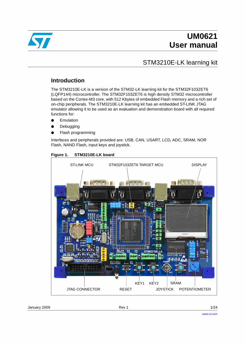
IntroductionThe STM3210E-LK is a version of the STM32-LK learning kit for the STM32F103ZET6 (LQFP144) microcontroller. The STM32F103ZET6 is high density STM32 microcontroller based on the Cortex-M3 core, with 512 Kbytes of embedded Flash memory and a rich set of on-chip peripherals. The STM3210E-LK learning kit has an embedded ST-LINK JTAG emulator allowing it to be used as an evaluation and demonstration board with all required functions for:
● Emulation
● Debugging
● Flash programming
Interfaces and peripherals provided are: USB, CAN, USART, LCD, ADC, SRAM, NOR Flash, NAND Flash, input keys and joystick.
Figure 1. STM3210E-LK board
ST-LINK MCU STM32F103ZET6 TARGET MCU
JTAG CONNECTOR RESET
KEY1 KEY2
JOYSTICK POTENTIOMETER
SRAM
DISPLAY
www.st.com
Contents UM0621
2/24
Contents
1 Overview . . . . . . . . . . . . . . . . . . . . . . . . . . . . . . . . . . . . . . . . . . . . . . . . . . 3
1.1 Features . . . . . . . . . . . . . . . . . . . . . . . . . . . . . . . . . . . . . . . . . . . . . . . . . . . 3
1.2 Product package . . . . . . . . . . . . . . . . . . . . . . . . . . . . . . . . . . . . . . . . . . . . 3
1.3 Functions . . . . . . . . . . . . . . . . . . . . . . . . . . . . . . . . . . . . . . . . . . . . . . . . . . 3
1.3.1 Emulator . . . . . . . . . . . . . . . . . . . . . . . . . . . . . . . . . . . . . . . . . . . . . . . . . 3
1.3.2 Evaluation system . . . . . . . . . . . . . . . . . . . . . . . . . . . . . . . . . . . . . . . . . . 4
2 Connectors and jumpers . . . . . . . . . . . . . . . . . . . . . . . . . . . . . . . . . . . . . 5
2.1 Connectors . . . . . . . . . . . . . . . . . . . . . . . . . . . . . . . . . . . . . . . . . . . . . . . . . 6
2.2 Jumpers . . . . . . . . . . . . . . . . . . . . . . . . . . . . . . . . . . . . . . . . . . . . . . . . . . . 7
3 Software installation . . . . . . . . . . . . . . . . . . . . . . . . . . . . . . . . . . . . . . . . 10
3.1 Embedded ST-LINK driver installation . . . . . . . . . . . . . . . . . . . . . . . . . . . 10
3.2 Demonstration program . . . . . . . . . . . . . . . . . . . . . . . . . . . . . . . . . . . . . . 10
4 Connecting power to the board . . . . . . . . . . . . . . . . . . . . . . . . . . . . . . . 11
5 Operating the demo program . . . . . . . . . . . . . . . . . . . . . . . . . . . . . . . . . 12
6 Troubleshooting . . . . . . . . . . . . . . . . . . . . . . . . . . . . . . . . . . . . . . . . . . . 14
6.1 Limitation with reset from IDE during debugging . . . . . . . . . . . . . . . . . . . 14
6.2 Analog/digital conversion (ADC) errors . . . . . . . . . . . . . . . . . . . . . . . . . . 14
7 Schematics . . . . . . . . . . . . . . . . . . . . . . . . . . . . . . . . . . . . . . . . . . . . . . . 15
7.1 Embedded ST-LINK . . . . . . . . . . . . . . . . . . . . . . . . . . . . . . . . . . . . . . . . . 15
7.2 Inputs and outputs . . . . . . . . . . . . . . . . . . . . . . . . . . . . . . . . . . . . . . . . . . 16
7.3 LCD . . . . . . . . . . . . . . . . . . . . . . . . . . . . . . . . . . . . . . . . . . . . . . . . . . . . . 17
7.4 MCU . . . . . . . . . . . . . . . . . . . . . . . . . . . . . . . . . . . . . . . . . . . . . . . . . . . . . 18
7.5 Memories . . . . . . . . . . . . . . . . . . . . . . . . . . . . . . . . . . . . . . . . . . . . . . . . . 19
7.6 Peripherals . . . . . . . . . . . . . . . . . . . . . . . . . . . . . . . . . . . . . . . . . . . . . . . . 20
7.7 SD Card . . . . . . . . . . . . . . . . . . . . . . . . . . . . . . . . . . . . . . . . . . . . . . . . . . 21
7.8 UART . . . . . . . . . . . . . . . . . . . . . . . . . . . . . . . . . . . . . . . . . . . . . . . . . . . . 21
UM0621 Contents
3/24
Revision history . . . . . . . . . . . . . . . . . . . . . . . . . . . . . . . . . . . . . . . . . . . . . . . . . . . . 22
Overview UM0621
4/24
1 Overview
1.1 Features● Supports IAR EWARM IDE
● Supports ARM RVMDK IDE
● Learning kit for STM32F103xCDE series ST Cortex M3 MCU
● Hardware and software architecture reference design
● Embedded ST-LINK for debug and programming STM32 target MCU
1.2 Product package
1.3 Functions
1.3.1 Emulator
● Embedded ST-LINK emulator, supports all STM32F10x series Cortex-M3
● USB 2.0 full speed, USB power supply
● Supports emulation of the on-board hardware and an external user system
● Download speed >2 kB/s
● Adaptive target system JTAG voltage level is 3.3 V
● The emulator can provide 5 V power (>100 mA) to the target system through pin 19 of the JTAG interface
Table 1. Product package list
Item Quantity
STM3210E-LK board 1
USB A-B type cable 1
DB9F/F RS-232 cable 1
Product CD-ROM 3
Package list 1
Quick start sheet 1
UM0621 Overview
5/24
1.3.2 Evaluation system
● STM32F103ZET6 ST Cortex-M3
● One 128 KB FSMC SRAM
● One 512 KB FSMC NOR Flash
● One 128 MB FSMC NAND Flash
● One 8 MB SPI Flash
● Two RS232 (DB9) connectors, with jumpers to disconnect them from the STM32
● One CAN (DB9) connector, with jumpers to disconnect it from the STM32
● Two B type USB connectors, with jumpers to disconnect them from the STM32
● One SD card socket, with jumpers to disconnect it from the STM32
● 8 MHz main clock oscillator with removable oscillator socket for optional 4~16 MHz
● 32 kHz oscillator, fixed
● One 128*64 dot-matrix LCD Module
● One I2C interface EEPROM, with jumpers to disconnect it from the STM32
● Four LEDs
● One channel potentiometer which can input an analog signal
● One 5-direction joystick
● Two GPIO user keys
● One RESET key
● Power supply selection:
– Powered by ST-LINK USB (CN1 connector)
– Powered by target MCU USB (CN4 connector)
● IR LED transmitter and receiver
Connectors and jumpers UM0621
6/24
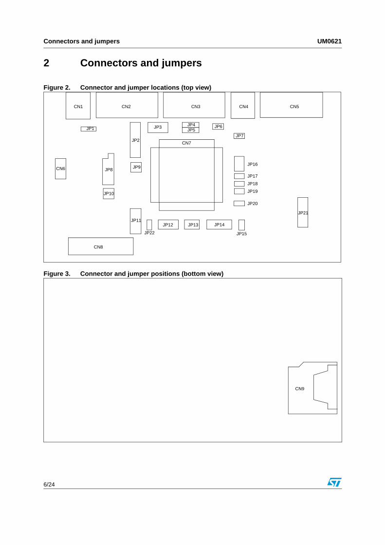
2 Connectors and jumpers
Figure 2. Connector and jumper locations (top view)
Figure 3. Connector and jumper positions (bottom view)
CN1 CN2 CN3 CN4 CN5
JP2JP7
JP4JP5
JP3JP1
JP9
JP10
JP8
JP6
JP16
JP17
JP18
JP19
JP20
JP21
JP13 JP14JP12JP11
JP22 JP15
CN6
CN7
CN8
CN9
UM0621 Connectors and jumpers
7/24
2.1 Connectors
Table 2. Connectors
ConnectorPCB
markingDescription
CN1 ST-LINKST-LINK USB connector, provides power when JP1 installed on the left 2 pins
CN2 USART1 RS-232 connector 0, connected via JP3 to target MCU
CN3 USART2 RS-232 connector 1, connected via JP3 to target MCU
CN4 USB USB device connector, connected via JP6 to target MCU
CN5 CAN CAN connector (DB9), connected via JP16 to target MCU
CN6 JTAG JTAG interface for ST-LINK (reserved for factory test purposes)
CN7 MCU External holes around target MCU for 112 I/Os, can be redefined by user
CN8External JTAG
ST-LINK JTAG external interface, connected via JP11 to target MCU (for debugging/programming target MCU)
CN9 SD Card SD Card socket, connected via JP2 & JP10 to the target MCU

Connectors and jumpers UM0621
8/24
2.2 JumpersFigure 4 shows all the jumpers on the STM3210E-LK. They are further described in two tables:
● Jumpers listed in Table 3 can be used to connect to or disconnect the peripherals on STM3210E-LK from the STM32 target MCU.
● Jumpers listed in Table 4 can be used to set different operating modes.
Figure 4. Jumper settings
Table 3. Jumpers for disconnecting peripherals from STM32
Jumper Peripheral Signals STM32 I/Os Description
JP2
SD card
MSD_D1 PC9 SD CARD Data Input
MSD_D0 PC8 Data Signal 0
MSD_CLK PC12 SD CARD Clock
MSD_CMD PD2 SD CARD Command
MSD_D3 PC11 SD CARD Data signal
MSD_D2 PC10 SD CARD Data signal
SD_PWR PB5 SD card power control
JP10MSD_DET PC2 MSD DET
MSD_WP PC3 MSD WP
JP3 USART
USART1_TX PA9 USART1 Send
USART1_RX PA10 USART1 Receive
USART2_TX PA2 USART2 Send
USART2_RX PA3 USART2 Receive
UM0621 Connectors and jumpers
9/24
JP8 MCU power
VBAT VBAT STM32 MCU VBAT
VDDA VDDA STM32 MCU VDDA
VDD VDD STM32 MCU VDD
VREF+ VREF+ STM32 MCU VREF+
VREF- VREF- STM32 MCU VREF-
JP9 32 kHz_OscOSC32_IN PC14 32K Oscillator input
OSC32_OUT PC15 32K Oscillator output
JP11 JTAG
JTDO PB3 Data Input
JTCK PA14 JTCK
JTMS PA13 JTMS
JTDI PA15 JTDI
NJTRST PB4 JTRST
JP12 LEDs
LD7 PF6 LD7
LD6 PF7 LD6
LD5 PF8 LD5
LD4 PF9 LD4
JP13 Keys
User_Button PB10 KEY4
Anti_Tamper PC13 KEY2
Wakeup PA0 KEY1
JP14 Joystick
JOY_DOWN PB15 Down
JOY_UP PB14 Up
JOY_LEFT PB13 Left
JOY_RIGHT PB12 Right
JOY_SEL PB11 Select
JP15 Potentiometer Potentiometer PC4 ADC Input
JP16 CAN
CAN_TX PB9 CAN Send
CAN_RX PB8 CAN Receive
CAN_SPCAN adjustable slope control (see Table 4 for details)
JP17 NOR Flash NOR_CS PG9 NOR Flash Enable
JP18 LCD LCD_CS PG12 LCD Enable
JP19 NAND NAND_CS PD7 NAND Flash Enable
JP20 SRAM SRAM_CS PG10 SRAM Enable
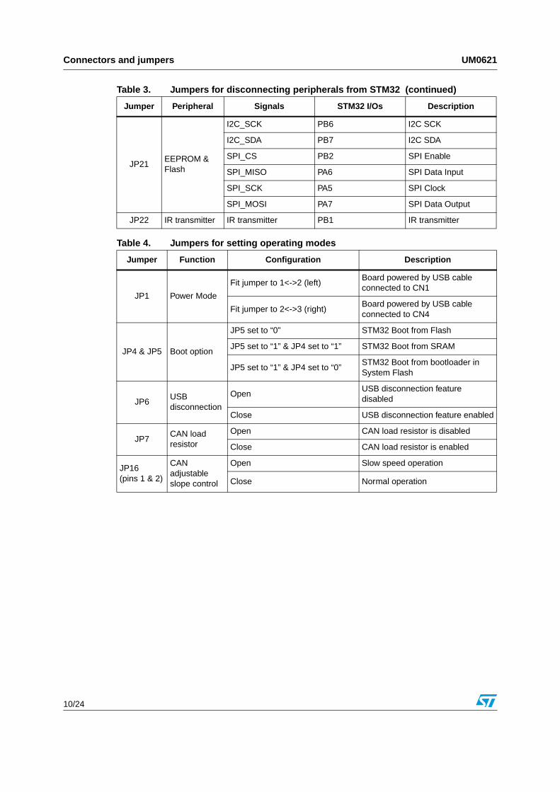
Table 3. Jumpers for disconnecting peripherals from STM32 (continued)
Jumper Peripheral Signals STM32 I/Os Description
Connectors and jumpers UM0621
10/24
JP21 EEPROM & Flash
I2C_SCK PB6 I2C SCK
I2C_SDA PB7 I2C SDA
SPI_CS PB2 SPI Enable
SPI_MISO PA6 SPI Data Input
SPI_SCK PA5 SPI Clock
SPI_MOSI PA7 SPI Data Output
JP22 IR transmitter IR transmitter PB1 IR transmitter
Table 4. Jumpers for setting operating modes
Jumper Function Configuration Description
JP1 Power Mode
Fit jumper to 1<->2 (left)Board powered by USB cable connected to CN1
Fit jumper to 2<->3 (right)Board powered by USB cable connected to CN4
JP4 & JP5 Boot option
JP5 set to “0” STM32 Boot from Flash
JP5 set to “1” & JP4 set to “1” STM32 Boot from SRAM
JP5 set to “1” & JP4 set to “0”STM32 Boot from bootloader in System Flash
JP6USB disconnection
OpenUSB disconnection feature disabled
Close USB disconnection feature enabled
JP7CAN load resistor
Open CAN load resistor is disabled
Close CAN load resistor is enabled
JP16(pins 1 & 2)
CAN adjustable slope control
Open Slow speed operation
Close Normal operation
Table 3. Jumpers for disconnecting peripherals from STM32 (continued)
Jumper Peripheral Signals STM32 I/Os Description
UM0621 Software installation
11/24
3 Software installation
3.1 Embedded ST-LINK driver installationThe STM3210E-LK box contains the CDs for both IAR and Keil IDEs. You can select either one according to your requirements. The embedded ST-LINK on STM3210E-LK is supported by the IDE from both IAR and Keil and can be used to debug and program the board. Install one of the IDEs by following the steps listed below:
1. Install IAR IDE EWARM or Keil IDE RVMDK from the CDs delivered in the STM3210E-LK box.
2. Select ST-LINK as the debugger in the IDE.
3.2 Demonstration programThe ST CD available in the STM3210E-LK box includes the Demo software and Software library with example programs for some on-board peripherals. It will help you get started quickly with STM32.
Connecting power to the board UM0621
12/24
4 Connecting power to the board
To start the demo without any debugging tool, the board must be powered on. There are two ways of doing this.
Note: Jumper JP6 must always be installed in either case.
To run the demo with an IAR or Keil IDE and ST-LINK, the first method must be used. With this method both the on-board ST-LINK and the STM32F103 target MCU are powered by the USB cable connected to the CN1 connector.
Method 1:
Two USB cables are needed when using this power-on method.
1. Place jumper JP1 in position 1-2.
2. Power on the board by attaching a USB cable to connector CN1.
3. After power on, the demo program starts.
4. Then, attach another USB cable to connector CN4 to demonstrate the USB mass storage application.
Method 2:
This method requires only one USB cable. This cable is also used by the USB mass storage application.
1. Place jumper JP1 in position 2-3.
2. Power on the board by attaching a USB cable to connector CN4.
3. After power on, the demo program starts.

UM0621 Operating the demo program
13/24
5 Operating the demo program
To use the demo, refer to the flowchart in Figure 5 and to the following procedure:
1. After power on, the ST logo is displayed on the LCD
2. There are two LCD demos, you can switch between them by pressing KEY1
3. Press KEY1 once to enter mode 1.
a) The orange LED (LD6) lights up to indicate mode 1.
b) In this mode, you can modify the input voltage to the target MCU’s analog to digital converter by rotating the potentiometer. The converted value is displayed on the LCD.
Figure 5. Demo program flowchart
Power on
ST logo displayed on LCD
Peripheral initialization
USBenumeration
Mass storage:2 partitions with SD cardand external SRAM
Press KEY1
LCD mode 1 LCD mode 2Orange LED on (LD6) Blue LED on (LD4)
Cursor on
ADC valueon LCD
Joystickoperation
Potentiometerrotated
This section is excluded from STM3210E-LK_USB configurations
This section is excluded from STM3210E-LK_NO_USB configurations
Operating the demo program UM0621
14/24
4. Press KEY1 a second time to enter mode 2.
a) The blue LED (LD4) lights up to indicate mode 2.
b) In this mode, you can operate the joystick.
– First, press in the joystick. A small block ‘cursor’ is displayed in the center of the LCD screen.
– You can move this cursor in 4 directions using the joystick.
– Pressing in the joystick makes the cursor return to the center of the screen. Always press in the joystick before moving the cursor in a new direction.
5. Press KEY1 again to enter mode1 again, and so on.
6. After 5 seconds, if no joystick movement or potentiometer change is detected, the LCD goes into screen saver mode and displays the ST logo. You can still see which mode you are in from the status of the LEDs.
7. A USB mass storage device is also implemented by the demo program with two storage partitions on two different media, one on an SD card and one on external SRAM through the FSMC (flexible static memory controller) of the STM32F103E.
Note: For RVMDK tool users, there are 3 project targets with different configurations that can be chosen freely in the drop-down menu. These are "STM3210E-LK_FULL", "STM3210E-LK-NO_USB" and "STM3210E-LK-USB". The 1st configuration has full functionality and can be used by full version RVMDK users, while the other 2 have limited functionality, as their names suggest, and can be used by evaluation version RVMDK users.
For STM3210E-LK_FULL configuration, all parts in the flowchart are present.
For STM3210E-LK_NO_USB configuration, parts surrounded by the dotted line rectangle on the left are not present.
For STM3210E-LK_USB configuration, parts surrounded by the dotted line rectangle on the right are not present.
UM0621 Troubleshooting
15/24
6 Troubleshooting
6.1 Limitation with reset from IDE during debuggingAs most IDEs (including IAR) only perform a software reset, they cannot reset the MCU thoroughly. After an IDE reset, parts of the board hardware may be in an uncertain state and this may lead to errors in some cases. For example a reset from the IDE may not reset the LCD properly.
Workaround
When debugging with IAR or MDK, to restart debugging without re-programming the chip and by using the IAR or MDK debugger reset:
● Use break to stop the program and reset the program counter (PC) to main and let it run again.
● To do this press the RESET key on the STM3210E-LK board after stopping the program with a break and before making a program counter (PC) reset.
6.2 Analog/digital conversion (ADC) errorsCorrect ADC conversion may be disturbed by USB communication and when an SD card is installed on the board as a removable USB mass storage device. When the SD card is plugged in, this effects the quality of the ADC power source. To prevent this the STM3210E-LK board would need additional on-board filtering and power separation. The demo firmware has a software filtering function, if this is not sufficient, use the workaround described below.
Workaround
Connect power to the STM3210E-LK board using the first method described in Section 4 on page 12. In this case you power on the board using a USB cable on connector CN1 and run the ADC part of the demo before attaching the USB cable to CN4 to run the USB mass storage part of the demo.
Schematics UM0621
16/24
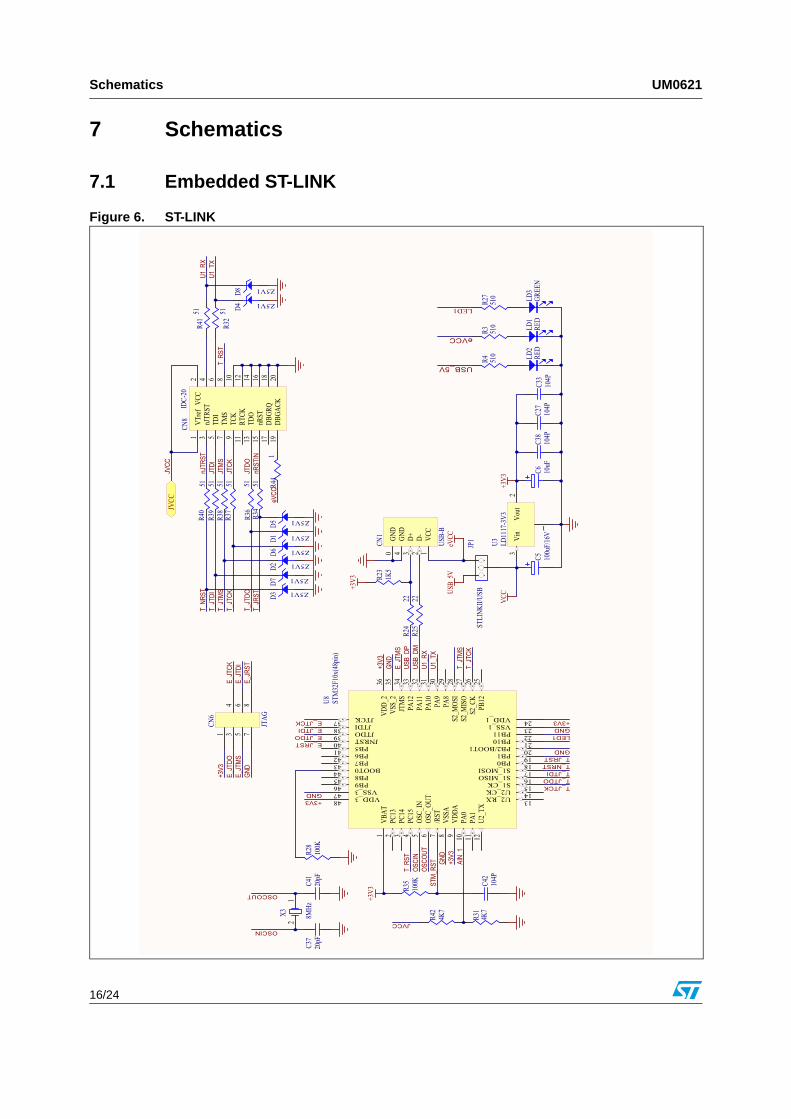
7 Schematics
7.1 Embedded ST-LINK
Figure 6. ST-LINKnJ
TRST
JTDI
JTMS
JTCK
R25
22R2
422
nRST
INJT
DO
VCC
1D-
2D+
3GN
D4
GND
0CN
1
USB-B
C38
104P
+3V3
C27
104P
C33
104P
LED1
JVCC
R42
4K7
R31
4K7
C5 100uF/16V
C6 10uF
eVCC Vin
3Vo
ut2
1
U3 LD1117-3V3
R23
1K5
+3V3
USB_
5V
JP1
STLINK
II/US
B
VBAT
1
PC13
2
PC14
3
PC15
4
OSC_
IN5
OSC_
OUT
6
/RST
7
VSSA
8
VDDA
9
PA0
10
PA1
11
U2_T
X12
U2_RX 13
U2_CK 14
S1_CK 15
S1_MISO 16
S1_MOSI 17
PB0 18
PB1 19
PB2/BOOT1 20
PB10 21
VSS_1 23
VDD_1 24
PB12
25
PB11 22
S2_C
K26
S2_M
ISO
27S2
_MOS
I28
PA8
29PA
930
PA10
31PA
1132
PA12
33JT
MS
34VS
S_2
35VD
D_2
36
JTCK37 JTDI38 JTDO39 JNRST40 PB541 PB642 PB743 BOOT044 PB845 PB946 VSS_347 VDD_348
U8 STM32F1
0x(48pin)
20pF
C37
20pF
C41
12
X3 8MHz
+3V3
USB_
DMUS
B_DP
STM_R
ST
T_JTCK
T_JT
CK
T_JTDOT_JTDI
T_JT
MS
E_JT
MSE_JTCKE_JTDIE_JTDOE_JRST
+3V3
+3V3
+3V3
+3V3
LED1
OSCIN
OSCO
UT
OSCIN
OSCOUT
U1_T
XU1
_RX
E_JT
DOE_
JTDI
E_JT
MS
E_JT
CK
E_JR
ST
T_NRSTT_JRST
LD3
GREE
N
VTref
1VC
C2
nJTR
ST3
4
TDI
56
TMS
78
TCK
910
RTCK
1112
TDO
1314
nRST
1516
DBGR
Q17
18
DBGA
CK19
20
CN8
IDC-20
eVCC
JVCC
JVCC
T_JT
CK
T_JT
DI
T_JT
DO
T_NR
ST
T_JT
MS
T_JR
ST
D5
Z5V1R34
51R3
651
R37
51R3
851
R39
51R4
051
D1
Z5V1
D6
Z5V1
D2
Z5V1
D7
Z5V1
D3
Z5V1
D4
Z5V1
D8
Z5V1
R32
51
R41
51
U1_T
XU1
_RX
AIN_
1
R44
1
C42
104P
R35
100K
R27
510
R28
100K
GND
GND
GND
GND
GND
GND
+3V3
LD1
RED
R3 510
14 6 8
3 5 7
CN6
JTAG
VCC
eVCC
LD2
RED
R4 510
USB_5VT_RS
T
T_RS
T
UM0621 Schematics
17/24
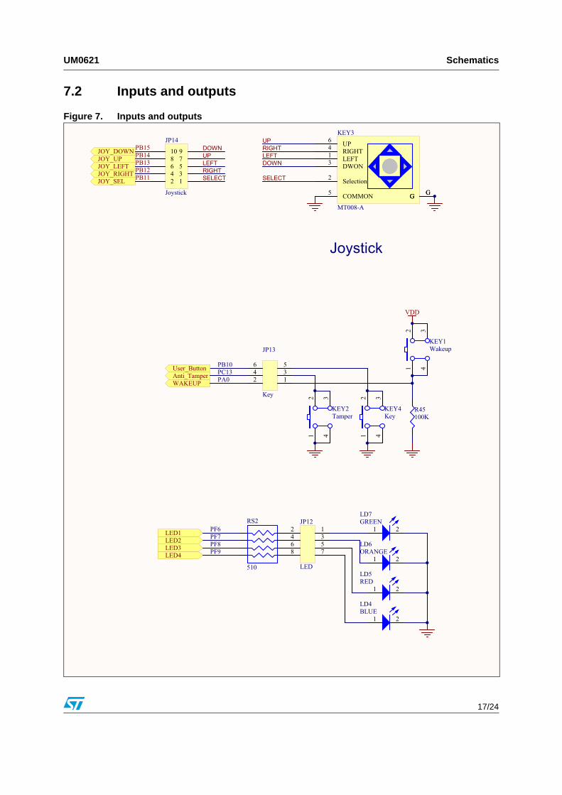
7.2 Inputs and outputs
Figure 7. Inputs and outputs
12
43
KEY4Key
12
43
KEY2Tamper
VDD
COMMON5
Selection2
DWON3 LEFT1 RIGHT4 UP6
G GG G
KEY3
MT008-A
Joystick
123456
JP13
Key
12345678910
JP14
Joystick
DOWNLEFTRIGHTUP
SELECT
DOWN
LEFTRIGHT
UP
SELECT
Anti_TamperWAKEUP
User_Button PB10PC13PA0
JOY_SEL
JOY_DOWN
JOY_LEFTJOY_RIGHT
JOY_UP
1 2
LD5RED
1 2
LD6ORANGE
1 2
LD4BLUE
1 2
LD7GREEN
LED4LED3
LED1LED2 PF7
PF6
PF9PF8
12345678
JP12
LED
PB11PB12PB13PB14PB15
12
43
KEY1Wakeup
R45100K
RS2
510
Schematics UM0621
18/24
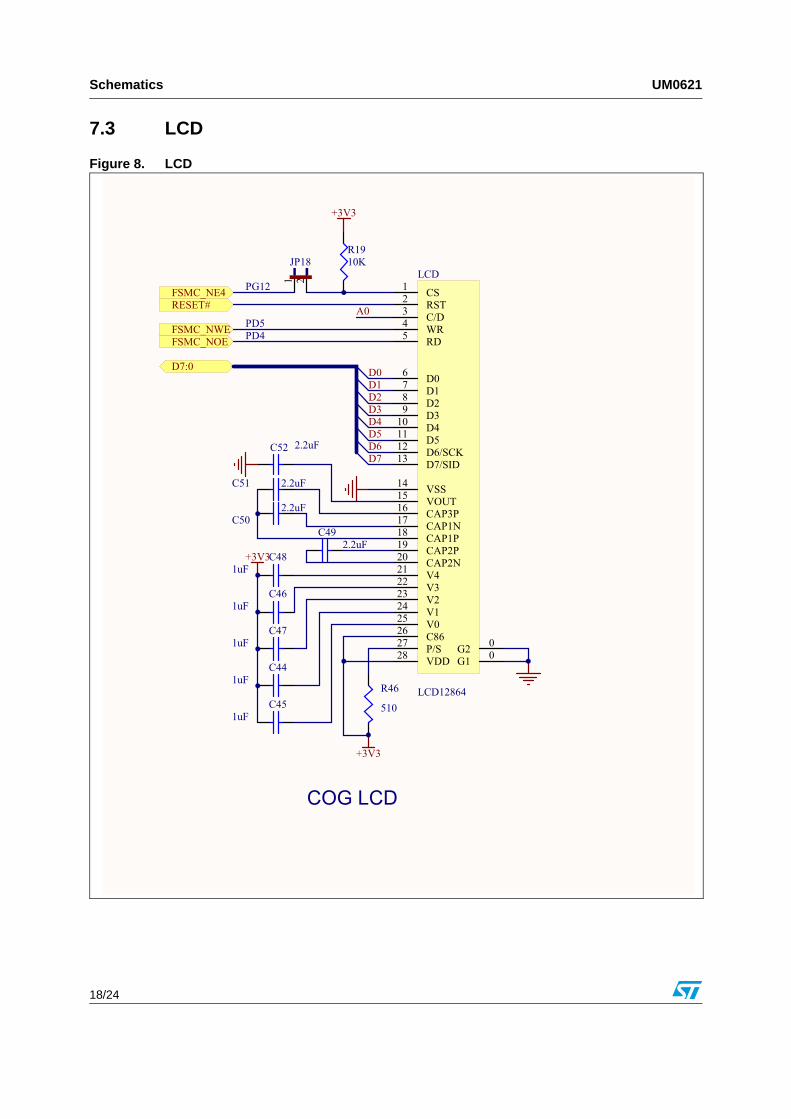
7.3 LCD
Figure 8. LCD
+3V3
RESET#
COG LCD
D7:0 D0D1D2D3D4D5D6D7
FSMC_NWEFSMC_NOE
A0
CS1
RST2
C/D3
WR4
RD5
D06
D17
D28
D39
D410
D511
D6/SCK12
D7/SID13
VSS14
VOUT15
CAP3P16
CAP1N17
CAP1P18
CAP2P19
CAP2N20
V421
V322
V223
V124
V025
C8626
P/S27
VDD28 G1 0G2 0
LCD
LCD12864
PG12
PD5PD4
FSMC_NE4
C52 2.2uF
C51 2.2uF
C502.2uF
C492.2uF
C481uF
C461uF
C471uF
C441uF
C451uF
1 2
JP18R1910K
+3V3
+3V3
R46
510
UM0621 Schematics
19/24
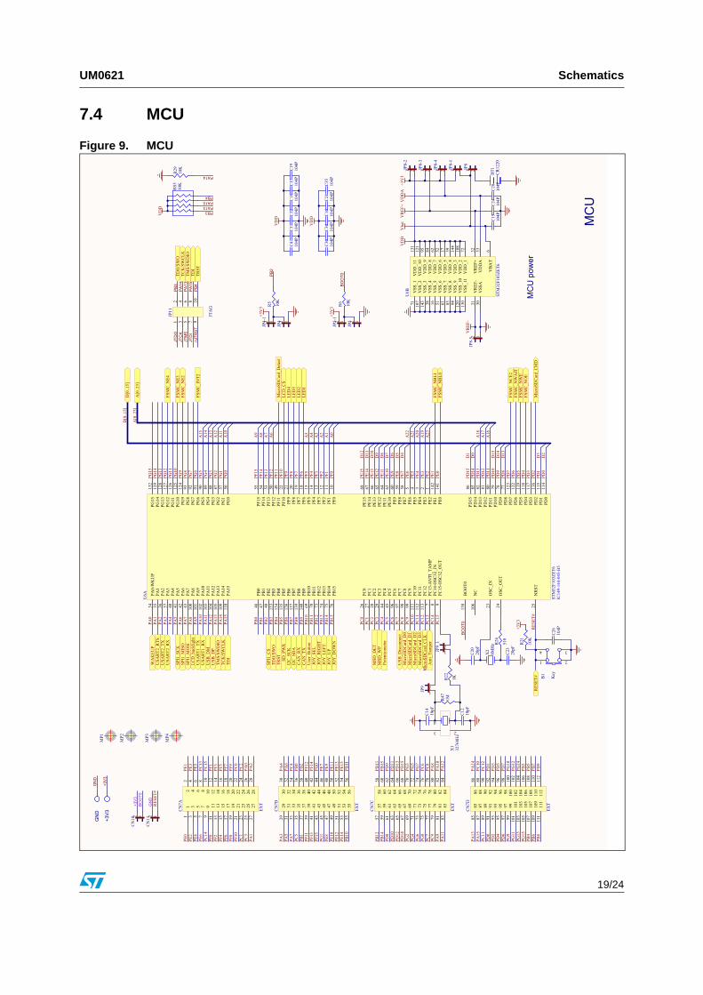
7.4 MCU
Figure 9. MCU
MCU
TDI
TMS/SW
DIO
TCK/SWCLK
USA
RT2
_RX
USA
RT2
_TX
USA
RT2
_RTS
USA
RT1
_TX
USA
RT1
_RX
LCD_backlight
WAKEU
P
SPI1_S
CK
SPI1_M
ISO
SPI1_M
OSI
USB
_DM
USB
_DP
PA0
PA1
PA2
PA3
PA4
PA5
PA6
PA7
PA8
PA9
PA10
PA11
PA12
PA13
PA14
PA15
TRST
TDO/SWO
SPI1_C
S
CAN_T
XCAN_R
X
I2C_S
CK
I2C_S
DA
PB0
PB1
PB2
PB3
PB4
PB5
PB6
PB7
PB8
PB9
PB10
PB11
PB12
PB13
PB14
PB15
+3V3
MicroSD
Card_CLK
MicroSD
Card_D0
MicroSD
Card_D1
MicroSD
Card_D2
MicroSD
Card_D3
Potentiometer
Anti_Ta
mper
4 1
3 2
X1
3276
8Hz
C12
10pF
C14
10pF
+3V3
C26
104P
C23
20pF
C20
20pF
X2
8MHz
RES
ET#
RES
ET#
FSMC_N
CE2
FSMC_N
WE
FSMC_N
OE
FSMC_N
WAIT
MicroSD
Card_CMD
FSMC_N
BL0
User_Button
LED3
LED1
LED2
USB
_Disconnect
JOY_S
EL
JOY_D
OWN
JOY_L
EFT
JOY_R
IGHT
JOY_U
P
FSMC_N
E2
FSMC_INT2
PC0
PC1
PC2
PC3
PC4
PC5
PC6
PC7
PC8
PC9
PC10
PC11
PC12
PC13
PC14
PC15
PD0
PD1
PD2
PD3
PD4
PD5
PD6
PD7
PD8
PD9
PD10
PD11
PD12
PD13
PD14
PD15
D2
D3
A16
D13
D14
D15
A17
A18
D0
D1
A19
A20
A21
A22
A23
D4
D5
D6
D7
D8
D9
D10
D11
D12
A0
A1
A2
A3
A4
A5
LED4
LCD_C
S
A6
A7
A8
A9
A10
A11
A12
A13
A14
A15
D[0..15]
A[0..23]
A[0..23]
D[0..15]
PF0
PF1
PF2
PF3
PF4
PF5
PF6
PF7
PF8
PF9
PF10
PF11
PF12
PF13
PF14
PF15
PE2
PE3
PE4
PE5
PE6
PE7
PE8
PE9
PE10
PE11
PE12
PE13
PE14
PE15
PE0
PE1
PG0
PG1
PG2
PG3
PG4
PG5
PG6
PG7
PG8
PG9
PG10
PG11
PG12
PG13
PG14
PG15
IC149-144-045-B5
PE2
1
PF2
12
OSC
_IN
23
PA0-WKUP
34
PC5
45
PG0
56
PE10
63PE
1164
PE3
2PE
43
PE5
4PE
65
PC13
-ANTI_T
AMP
7
PC14-O
SC32_IN
8
PC15
-OSC
32_O
UT
9
PF0
10PF
111
PF3
13PF
414
PF5
15PF
618
PF7
19PF
820
PF9
21PF
1022
OSC
_OUT
24
NRST
25
PC0
26
PC1
27
PC2
28
PC3
29
PA1
35
PA2
36
PA3
37
PA4
40
PA5
41
PA6
42
PA7
43
PC4
44
PB0
46
PB1
47
PB2
48
PF11
49PF
1250
PF13
53PF
1454
PF15
55
PG1
57
PE7
58PE
859
PE9
60
PE12
65
PB15
76
PG2
87
PC8
98
PA14
109
PG11
126
PG12
127
PG13
128
PE13
66PE
1467
PE15
68
PB10
69
PB11
70
PB12
73
PB13
74
PB14
75
PD8
77PD
978
PD10
79PD
1180
PD12
81PD
1382
PD14
85PD
1586
PG3
88PG
489
PG5
90PG
691
PG7
92PG
893
PC6
96
PC7
97
PC9
99
PA8
100
PA9
101
PA10
102
PA11
103
PA12
104
PA13
105
NC
106
PA15
110
PC10
111
PC11
112
PC12
113
PD0
114
PD1
115
PD2
116
PD3
117
PD4
118
PD5
119
PD6
122
PD7
123
PG9
124
PG10
125
PG14
129
PB7
137
BOOT0
138
PB8
139
PB9
140
PE0
141
PE1
142
PG15
132
PB3
133
PB4
134
PB5
135
PB6
136
U6A
STM32F1
03ZE
T6
MicroSD
Card_Detect
FSMC_N
E3
FSMC_N
E4
FSMC_N
BL1
PB2
VREF
-
C28
104P+3
V3
VDDA
VDD
BT1
CR12
20
Vbat
VREF
+ C24
104P
VDD_7
62
VBAT
6
VSS
_516
VDD_5
17
VSS
A30
VREF
-31
VREF
+32
VDDA
33
VSS
_438
VDD_4
39
VSS
_651
VDD_6
52
VSS
_761
VSS
_10
120
VSS
_171
VDD_1
72
VSS
_883
VDD_8
84
VSS
_994
VDD_9
95VSS
_2107
VDD_2
108
VDD_1
0121
VSS
_3143
VDD_3
144
VSS
_11
130
VDD_1
1131
U6B
STM32F1
03ZE
T6
MCU pow
er
1 2JP8-3
12JP8-5
1 2JP8-2
1 2JP8-4
1 2JP8-1
1 2JP8
C15
104P
12JP412
JP4-1
BOOT0
+3V3
BOOT0
12JP512
JP5-1
12
JP9
12
JP9_1
1 2
4 3
B1
Key
VDD
JTDI
JTMS
JTCK
JTDO
nJTR
ST
R29
10K
RS3
10K
PA13
PA15
PB3
PA14
PB4
PA13PA15
PB3
PA14
PB4
12
34
56
78
910
JP11
JTAG
TDI
TRST
TMS/SW
DIO
TCK/SWCLK
TDO/SWO
C3
104P
C4
104P
C32
104P
C18
104P
C17
104P
C34
104P
C36
104P
C16
104P
C21
104P
C35
104P
C19
104P
VDD
VDD
11
22
33
44
55
66
77
88
99
1010
1111
1212
1313
1414
1515
1616
1717
1818
1919
2020
2121
2222
2323
2424
2525
2626
2727
2828
CN7A
EXT 29
2930
30
3131
3232
3333
3434
3535
3636
3737
3838
3939
4040
4141
4242
4343
4444
4545
4646
4747
4848
4949
5050
5151
5252
5353
5454
5555
5656
CN7B
EXT 57
5758
58
5959
6060
6161
6262
6363
6464
6565
6666
6767
6868
6969
7070
7171
7272
7373
7474
7575
7676
7777
7878
7979
8080
8181
8282
8383
8484
CN7C
EXT 85
8586
86
8787
8888
8989
9090
9191
9292
9393
9494
9595
9696
9797
9898
9999
100
100
101
101
102
102
103
103
104
104
105
105
106
106
107
107
108
108
109
109
110
110
111
111
112
112
CN7D
EXT
PE2
PE3
PE4
PE5
PE6
PE7
PE8
PE9
PE10
PE11
PE12
PE13
PE14
PE15
PE0
PE1
PF0
PF1
PF2
PF3
PF4
PF5
PF6
PF7
PF8
PF9
PF10
PF11
PF12
PF13
PF14
PF15
PG0
PG1
PG2
PG3
PG4
PG5
PG6
PG7
PG8
PG9
PG10
PG11
PG12
PG13
PG14
PG15
PD0
PD1
PD2
PD3
PD4
PD5
PD6
PD7
PD8
PD9
PD10
PD11
PD12
PD13
PD14
PD15
PC0
PC1
PC2
PC3
PC4
PC5
PC6
PC7
PC8
PC9
PC10
PC11
PC12
PC13
PC14
PC15
PB0
PB1
PB2
PB3
PB4
PB5
PB6
PB7
PB8
PB9
PB10
PB11
PB12
PB13
PB14
PB15
PA0
PA1
PA2
PA3
PA4
PA5
PA6
PA7
PA8
PA9
PA10
PA11
PA12
PA13
PA14
PA15
SD_P
WR R
26
510
R21
10K
R5
10K
R6
10K
MSD
_DET
MSD
_WP
GND
+3V3
+3V3
GND
R47
1MR22
1K
MP1
MP2
MP3
MP4
12CN1112
CN10
RES
ET#
GND
BOOT0
+3V3
Schematics UM0621
20/24
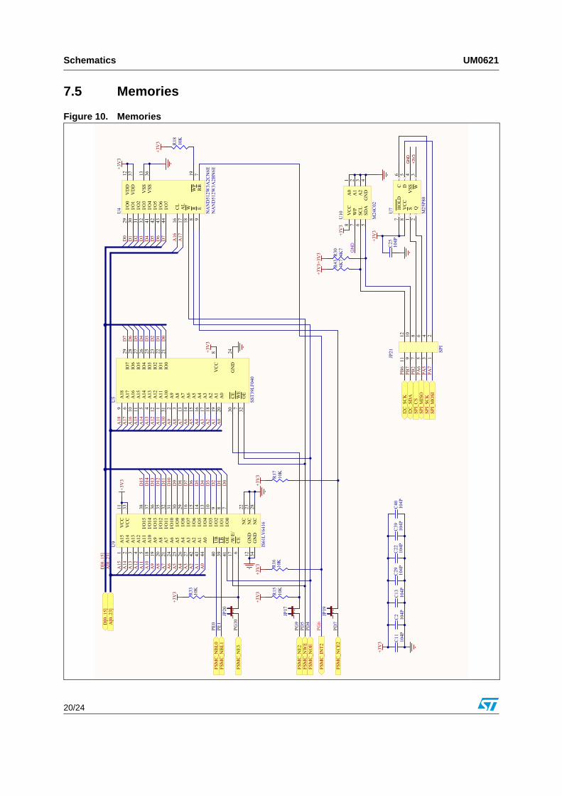
7.5 Memories
Figure 10. Memories
+3V3
A1
A2
A3
A4
A5
A6
A7
A8
A9
A10
A11
A12
A13
A14
A15
A1
A2
A3
A4
A5
A6
A7
A8
A9
A10
A11
A12
A13
A14
A15
A16
A17
A18
A[0..23]
D[0..15]
RB
7R
8
E9
VDD
12
VSS
13
CL
16
AL
17
W18
WP
19
I/O0
29
I/O1
30
I/O2
31
I/O3
32
VSS
36
VDD
37
I/O4
41
I/O5
42
I/O6
43
I/O7
44
U4
NAND51
2W3A
2CN6E+3
V3
A16
A17
FSMC_N
E3
FSMC_N
E2
FSMC_N
CE2
FSMC_N
WE
FSMC_N
OE
D[0..15]
A[0..23]
C22
104P
C39
104P
C2
104P
+3V3
+3V3
C11
104P
C29
104P
C40
104P
+3V3
A0
A0
+3V3
+3V3
D0
D1
D2
D3
D4
D5
D6
D7
D8
D9
D10
D11
D12
D13
D14
D15
D0
D1
D2
D3
D4
D5
D6
D7
D0
D1
D2
D3
D4
D5
D6
D7
+3V3
C13
104P
NAND51
2W3A
2BN6E
PE1
PE0
PD5
PG9
PD4
PG10
PD7
PG6
FSMC_N
BL0
FSMC_N
BL1
FSMC_INT2
A15
1
A14
2
A13
3
A12
4
A11
5
CE
6
I/O0
7I/O
18
I/O2
9I/O
310
VCC
11
I/O4
13I/O
514
I/O6
15I/O
716
/W/E/
17
GND
12
A10
18
A9
19
A8
20
A7
21
NC
22
NC
23
A6
24
A5
25
A4
26
A3
27
NC
28
I/O8
29I/O
930
I/O10
31I/O
1132
VCC
33
GND
34
I/O12
35I/O
1336
I/O14
37I/O
1538
LB39
UB
40
OE
41
A2
42
A1
43
A0
44
U9
IS61LV
6416
+3V3
A11
1
A9
2
A8
3
A13
4A14
5
A17
6
WE
7
VCC
8
A18
9
A16
10
A15
11
A12
12
A7
13
A6
14
A5
15
A4
16
A3
17
A2
18
A1
19
A0
20
IO0
21IO
122
IO2
23
GND
24
IO3
25IO
426
IO5
27IO
628
IO7
29
CE
30
A10
31
OE
32
U5
SST3
9LF0
40
R15
10K
R16
10K
R33
10K
R17
10K
R18
10K
12
JP17
12
JP20
12
JP19
+3V3
C25
104P
HOLD
7
VCC
8
S1
Q2
W3
VSS
4D
5C
6U7
M25
P80
SPI_CS
SPI_SC
KSP
I_MISO
SPI_MOSI
PB2
PA5
PA6
PA7
12
34
56
78
910
1112
JP21 SP
I
GND
+3V3
A0
1
A1
2
A2
3
GND
4SD
A5
SCL
6WP
7VCC
8U10
M24
C02
+3V3
R30
4K7
R43
4K7+3V3
+3V3
I2C_S
CK
I2C_S
DA
PB6
PB7
GND
UM0621 Schematics
21/24
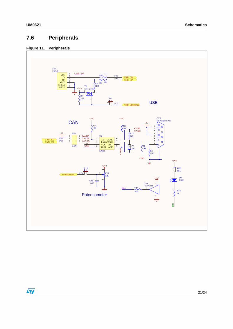
7.6 Peripherals
Figure 11. Peripherals
VCC 1
D- 2
D+ 3
GND 4
SHELL 0
SHELL 0
CN4USB-B
R710K
+3V32
31
T1SI2301DS
+3V3
13
2 RV110K
+3V3
USB_DMUSB_DP
USB_Disconnect
Potentiometer
Potentiometer
USB
PA12PA11
PB8PB9
PC4
C43104P
162738495
CN5DB9-male CAN
R81K5
1 2
JP6
R9 22
R10 22
CANCANLCANH
TX1
ASC 8GND2
CANH 7
VCC3 RXO4
RX1 5
CANL 6U2
L9616
GND+3V3
CANTXCANRX
R1310K
R12120
JP7Load
1 23 45 6
JP16
CAN
R1410K
+3V3 +3V3
CAN_TXCAN_RX
CANSP
CANSP
R110K
R210K
1 2
JP15
USB_5V
PC7
R481K
+3V3
R49
10K
PB1
JP22SEL
D9TXD
+3V3
PB0 1
23D10TOP1838
Schematics UM0621
22/24
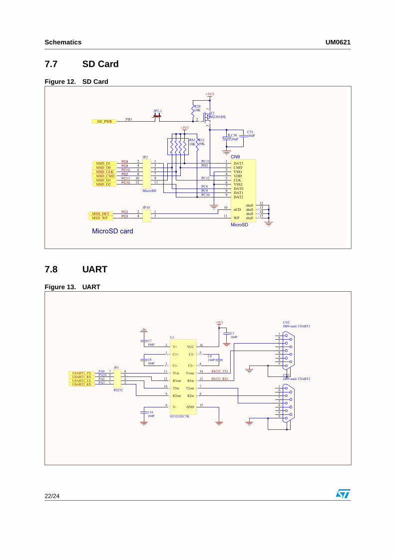
7.7 SD Card
Figure 12. SD Card
7.8 UART
Figure 13. UART
MSD_CLKMSD_CMD
MicroSD card
MSD_D0MSD_D1
MSD_D2MSD_D3
MSD_DET
+3V3C31104PC30
10uF
SD_PWR
+3V3
R2010K
2
31
T2SI2301DS
RS110K
R1110K
1 2
JP2-1
123456789101112
JP2
MicroSD
MSD_WP
PC8PC9
PC10PC11
PC12PD2
PB5
DAT31
CMD2
VSS13
VDD4
CLK5
VSS26
DAT07
DAT18
DAT29
nCD10
WP11
shell 12
shell 13
shell 14
shell 15
CN9
MicroSD
1234
JP10
PC11
PC8PC9PC10
PC12
PD2
PC2PC3
162738495
CN3DB9-male USART2
R2out9 R2in 8
T1in11
R1out12
T1out 14
R1in 13
T2in10 T2out 7
C1+1
C1-3 C2+ 4
C2- 5
V+2
V-6
VCC 16
GND 15
U1
ST3232ECTR
C1104P
C8104P
C9104P
C7104P
C10104P
+3V3
162738495
CN2DB9-male USART1
RS232_RX1
RS232_TX1
USART2_RXUSART2_TX
USART1_TXUSART1_RX PA2
PA3
PA9PA10
1 23 45 67 8
JP3
RS232

UM0621 Revision history
23/24
Revision history
Table 5. Document revision history
Date Revision Changes
13-Jan-2009 1 Initial release.
UM0621
24/24
Please Read Carefully:
Information in this document is provided solely in connection with ST products. STMicroelectronics NV and its subsidiaries (“ST”) reserve theright to make changes, corrections, modifications or improvements, to this document, and the products and services described herein at anytime, without notice.
All ST products are sold pursuant to ST’s terms and conditions of sale.
Purchasers are solely responsible for the choice, selection and use of the ST products and services described herein, and ST assumes noliability whatsoever relating to the choice, selection or use of the ST products and services described herein.
No license, express or implied, by estoppel or otherwise, to any intellectual property rights is granted under this document. If any part of thisdocument refers to any third party products or services it shall not be deemed a license grant by ST for the use of such third party productsor services, or any intellectual property contained therein or considered as a warranty covering the use in any manner whatsoever of suchthird party products or services or any intellectual property contained therein.
UNLESS OTHERWISE SET FORTH IN ST’S TERMS AND CONDITIONS OF SALE ST DISCLAIMS ANY EXPRESS OR IMPLIEDWARRANTY WITH RESPECT TO THE USE AND/OR SALE OF ST PRODUCTS INCLUDING WITHOUT LIMITATION IMPLIEDWARRANTIES OF MERCHANTABILITY, FITNESS FOR A PARTICULAR PURPOSE (AND THEIR EQUIVALENTS UNDER THE LAWSOF ANY JURISDICTION), OR INFRINGEMENT OF ANY PATENT, COPYRIGHT OR OTHER INTELLECTUAL PROPERTY RIGHT.
UNLESS EXPRESSLY APPROVED IN WRITING BY AN AUTHORIZED ST REPRESENTATIVE, ST PRODUCTS ARE NOTRECOMMENDED, AUTHORIZED OR WARRANTED FOR USE IN MILITARY, AIR CRAFT, SPACE, LIFE SAVING, OR LIFE SUSTAININGAPPLICATIONS, NOR IN PRODUCTS OR SYSTEMS WHERE FAILURE OR MALFUNCTION MAY RESULT IN PERSONAL INJURY,DEATH, OR SEVERE PROPERTY OR ENVIRONMENTAL DAMAGE. ST PRODUCTS WHICH ARE NOT SPECIFIED AS "AUTOMOTIVEGRADE" MAY ONLY BE USED IN AUTOMOTIVE APPLICATIONS AT USER’S OWN RISK.
Resale of ST products with provisions different from the statements and/or technical features set forth in this document shall immediately voidany warranty granted by ST for the ST product or service described herein and shall not create or extend in any manner whatsoever, anyliability of ST.
ST and the ST logo are trademarks or registered trademarks of ST in various countries.
Information in this document supersedes and replaces all information previously supplied.
The ST logo is a registered trademark of STMicroelectronics. All other names are the property of their respective owners.
© 2009 STMicroelectronics - All rights reserved
STMicroelectronics group of companies
Australia - Belgium - Brazil - Canada - China - Czech Republic - Finland - France - Germany - Hong Kong - India - Israel - Italy - Japan - Malaysia - Malta - Morocco - Singapore - Spain - Sweden - Switzerland - United Kingdom - United States of America
www.st.com