Embed Size (px)
Citation preview

PE29101Document Category: Product SpecificationUltraCMOS® High-speed FET Driver, 40 MHz
Features• High- and low-side FET drivers
• Dead-time control
• Fast propagation delay, 11 ns
• Internal gate overvoltage management
• Sub-nanosecond rise and fall time
• 2A/4A peak source/sink current
• Package – flip chip
Applications• DC–DC conversions
• AC–DC conversions
• Wireless power
• LiDAR
Product DescriptionThe PE29101 integrated high-speed driver is designed to control the gates of external power devices, such as enhancement mode gallium nitride (GaN) FETs. The outputs of the PE29101 are capable of providing switching transition speeds in the sub-nanosecond range for switching applications up to 40 MHz. High switching speeds result in smaller peripheral components and enable new applications such as wireless power charging.
The PE29101 operates from 4V to 6.5V and can support a high side floating supply voltage of 80V. An optional internal synchronous bootstrap circuit limits overcharging of the bootstrap capacitor during reverse body diode conduction, preventing the GaN FETs from exceeding their maximum gate-to-source voltage rating. The PE29101 also features a dead-time controller that allows timing of the LS and HS gates to eliminate any large shoot-through currents that could dramatically reduce the efficiency of the circuit and potentially damage the transistors.
The PE29101 is available in a flip chip package and is manufactured on Peregrine’s UltraCMOS process, a patented advanced form of silicon-on-insulator (SOI) technology, offering the performance of GaAs with the economy and integration of conventional CMOS.
Figure 1 • PE29101 Functional Diagram
RDHL
GND
IN
EN
VDDSYNC
VDD
HSGPU
HSGPD
HSS
HSB
LSB
LSSRDLH
LSO
LSGPU
LSGPD
DeadTime
ControllerLogic
UVLO
LevelShifter
OutputDriver
LevelShifter
OutputDriver
Sync BootSwitch
END OF LI
FE
©2018, pSemi Corporation. All rights reserved. • Headquarters: 9369 Carroll Park Drive, San Diego, CA, 92121
Product Specification DOC-78681-7 – (07/2019)www.psemi.com

PE29101High-speed FET Driver
Absolute Maximum RatingsExceeding absolute maximum ratings listed in Table 1 may cause permanent damage. Operation should be restricted to the limits in Table 2. Operation between operating range maximum and absolute maximum for extended periods may reduce reliability.
ESD PrecautionsWhen handling this UltraCMOS device, observe the same precautions as with any other ESD-sensitive devices. Although this device contains circuitry to protect it from damage due to ESD, precautions should be taken to avoid exceeding the rating specified in Table 1.
Latch-up ImmunityUnlike conventional CMOS devices, UltraCMOS devices are immune to latch-up.
Table 1 • Absolute Maximum Ratings for PE29101
Parameter/Condition Min Max Unit
Low-side bias (LSB) to low-side source (LSS) –0.3 7 V
High-side bias (HSB) to high-side source (HSS) –0.3 7 V
Input signal –0.3 7 V
HSS to LSS –5 100 V
ESD voltage HBM(*), all pins 1000 V
Note: * Human body model (JEDEC JS–001, Table 2A).
END OF LI
FE
Page 2 of 15 DOC-78681-7 – (07/2019)www.psemi.com

PE29101High-speed FET Driver
Recommended Operating ConditionsTable 2 lists the recommended operating conditions for the PE29101. Devices should not be operated outside the recommended operating conditions listed below.
Table 2 • Recommended Operating Conditions for PE29101
Parameter Min Typ Max Unit
Supply for driver front-end, VDD 4.0 5.0 6.5 V
Supply for high-side bias (HSB) to high-side source (HSS) 4.0 5.0 6.5 V
Supply for low-side bias (LSB) to low-side source (LSS) 4.0 5.0 6.5 V
Logic HIGH for control input 1.6 6.5 V
Logic LOW for control input 0 0.6 V
HSS range 0 80 V
Operating temperature –40 +105 °C
Junction temperature –40 +125 °C
END OF LI
FE
DOC-78681-7 – (07/2019) Page 3 of 15www.psemi.com

PE29101High-speed FET Driver
Electrical SpecificationsTable 3 provides the key electrical specifications @ +25 °C, VDD = 5V, 100 pF load; RDHL and RDLH are ±1% tolerance unless otherwise specified.
Table 3 • DC Characteristics
Parameter Condition Min Typ Max Unit
DC Characteristics
VDD quiescent current VDD = 5V, RDHL = RDLH = 80.6 kΩ 0.9 mA
HSB quiescent current HSB = 5V 2.5 mA
LSB quiescent current LSB = 5V 2.5 mA
Total quiescent currentVDD =HSB=LSB=5V, RDHL = RDLH =
80.6 kΩ5.9 8.0 mA
VDD quiescent current VDD = 6.5V, RDHL = RDLH = 80.6 kΩ 1.3 mA
HSB quiescent current HSB = 6.5V 3.8 mA
LSB quiescent current LSB = 6.5V 3.9 mA
Total quiescent currentVDD =HSB=LSB=6.5V, RDHL = RDLH =
80.6 kΩ9.0 11.5 mA
Under Voltage Lockout
Under voltage release (rising) 3.6 3.9 V
Under voltage hysteresis 400 mV
Gate Drivers
HSGPU/LSGPU pull-up resistance VDD = 6.5V, RDHL = RDLH = 80.6 kΩ 1.8 Ω
HSGPD/LSGPD pull-down resistance VDD = 6.5V 1.5 Ω
VDDSYNC resistance 4.5 Ω
HSGPU/LSGPU leakage current HSB–HSGPU = 5V, LSB–LSGPU = 5V 10 µA
HSGPD/LSGPD leakage current HSGPD–HSS = 5V/LSGPD–HSS = 5V 50 µA
Dead-time Control
Dead-time control voltages HSB=LSB, 80.6 kΩ resistor to GND 1.4 V
Dead-time from HSG going low to LSG going high
RDHL = 30 kΩ 0.8 ns
RDHL = 80.6 kΩ 3.3 ns
RDHL = 150 kΩ 6.5 ns
RDHL = 255 kΩ 11.1 nsEND OF LI
FE
Page 4 of 15 DOC-78681-7 – (07/2019)www.psemi.com

PE29101High-speed FET Driver
Control LogicTable 4 provides the control logic truth table for the PE29101.
Dead-time from LSG going low to HSG going high
RDLH = 30 kΩ 0.2 ns
RDLH = 80.6 kΩ 2.6 ns
RDHL = 150 kΩ 5.6 ns
RDHL = 255 kΩ 10.0 ns
Switching Characteristics
LSG turn-off propagation delay 11.0 ns
HSG rise time 10%–90% with 100pF load 1.0 ns
LSG rise time 10%–90% with 100pF load 1.0 ns
HSG fall time 10%–90% with 100pF load 1.0 ns
LSG fall time 10%–90% with 100pF load 1.0 ns
Minimum output pulse width RDLH = RDLH = 30 kΩ 2.0 4.0 ns
Max switching frequency @ 50% duty cycle
RDHL = RDLH = 80.6 kΩ 40 47 MHz
Table 3 • DC Characteristics (Cont.)
Parameter Condition Min Typ Max Unit
Table 4 • Truth Table for PE29101
EN IN HSGPU–HSS HSGPD–HSS LSGPU–LSS LSGPD–LSS
L L Hi–Z L H Hi–Z
L H H Hi–Z Hi–Z L
H L Hi–Z L Hi–Z L
H H Hi–Z L Hi–Z L
END OF LI
FE
DOC-78681-7 – (07/2019) Page 5 of 15www.psemi.com

PE29101High-speed FET Driver
Typical Performance DataFigure 2 through Figure 4 show the typical performance data @ +25 °C, VDD = 5V, load = 100 pF capacitor, unless otherwise specified.
Figure 2 • Total Quiescent Current
0
1
2
3
4
5
6
7
8
9
10
-40 25 105
Tota
l Qui
esce
nt C
urre
nt (m
A)
VDD = 4.0V VDD = 5.0V VDD = 6.5V
Temperature (°C)
END OF LI
FE
Page 6 of 15 DOC-78681-7 – (07/2019)www.psemi.com

PE29101High-speed FET Driver
Figure 3 • UVLO Threshold
2.9
3
3.1
3.2
3.3
3.4
3.5
3.6
3.7
3.8
-40 25 105
UVL
O T
hres
hold
(V)
UVLO Rising UVLO Falling
Temperature (°C)
Figure 4 • Dead Time
Dea
d-tim
e (n
s)
Temperature (°C)
0.00
2.00
4.00
6.00
8.00
10.00
12.00
-60 -40 -20 0 20 40 60 80 100 120
TDHL_ns 30K TDHL_ns 80.6K TDHL_ns 150K TDHL_ns 255K
TDLH_ns 30K TDLH_ns 80.6K TDLH_ns 150K TDLH_ns 255K
END OF LI
FE
DOC-78681-7 – (07/2019) Page 7 of 15www.psemi.com

PE29101High-speed FET Driver
Test DiagramFigure 5 shows the test circuit used to characterize the PE29101.
Figure 5 • Test Circuit for PE29101
RDHL
GND
PWMIN
EN
HSB
VDD
HSGPU
HSGPD
HSS
LSB
LSS
RDLH
LevelShifter
LSO
VDD
100 pF
LSGPU
LSGPD
DeadTime
ControllerLogic
UVLO
100 pF
LevelShifter
OutputDriver
OutputDriver
VDDSYNCSync BootSwitch
END OF LI
FE
Page 8 of 15 DOC-78681-7 – (07/2019)www.psemi.com

PE29101High-speed FET Driver
Theory of Operation
GeneralThe PE29101 is intended to drive both the high-side (HS) and the low-side (LS) gates of external power transistors, such as enhancement-mode GaN FETs, for power management applications. The PE29101 is suited for applications requiring higher switching speeds due to the reduced parasitic properties of the high resistivity insulating substrate inherent with Peregrine’s UltraCMOS process.
The driver uses a single-ended pulse width modulation (PWM) input that feeds a dead-time controller, capable of generating a small and accurate dead-time. The propagation delay of the dead-time controller must be small to meet the fast switching requirements when driving GaN FETs. The differential outputs of the dead-time controller are then level-shifted from a low-voltage domain to a high-voltage domain required by the output drivers.
Each of the output drivers includes two separate pull-up and pull-down outputs allowing independent control of the turn-on and turn-off gate loop resistance. The low impedance output of the drivers improves external power FETs switching speed and efficiency, and minimizes the effects of the voltage rise time (dv/dt) transients.
Under-voltage LockoutAn internal under-voltage lockout (UVLO) feature prevents the PE29101 from powering up before input voltage rises above the UVLO threshold of 3.6V (typ), and 400 mV (typ) of hysteresis is built in to prevent false triggering of the UVLO circuit. The UVLO must be cleared and the EN pin must be released before the part will be enabled.
Dead-time AdjustmentThe PE29101 features a dead-time adjustment that allows the user to control the timing of the LS and HS gates to eliminate any large shoot-through currents, which could dramatically reduce the efficiency of the circuit and potentially damage the GaN FETs. Two external resistors control the timing of outputs in the dead-time controller block. The timing waveforms are illustrated in Figure 6.
The dead-time resistors only affect the LS output; the HS output will always equal the duty-cycle of the input. The HS FET gate node will track the duty cycle of the PWM input, as both rising and falling edges are shifted in the same direction. The LS FET gate node duty cycle can be controlled with the dead-time resistors as each resistor will move the rising and falling edges in opposite directions. RDLH will change the dead-time from low-side gate (LSG) falling to high-side gate (HSG) rising and RDHL will change the dead-time from HSG falling to LSG rising. Figure 7 shows the resulting dead-time versus the external resistor values
High-side Gate Overvoltage ProtectionIn cases where the GaN transistor body diode conduction is significantly longer than the bootstrap diode turn-on time, overcharging of the bootstrap capacitor can develop. The resulting overvoltage on the high-side supply may exceed the specified operating range of the transistor. The PE29101 features an internal synchronous bootstrap protection circuit (pin 4) designed to limit overcharging of the bootstrap capacitor during reverse body diode conduction.END O
F LIFE
DOC-78681-7 – (07/2019) Page 9 of 15www.psemi.com

PE29101High-speed FET Driver
Figure 6 and Figure 7 provide the dead-time description for the PE29101.
Figure 6 • Typical Dead-time Description
IN
HSG-HSS
LSG-LSStDHLtDLH
Figure 7 • Dead-time vs. Dead-time Resistor
0
2
4
6
8
10
12
0 50 100 150 200 250 300
Dea
d-tim
e be
twee
n H
SG a
nd L
SG (n
s)
Dead-time Resistance (kΩ)
TDLH TDHL
END OF LI
FE
Page 10 of 15 DOC-78681-7 – (07/2019)www.psemi.com

PE29101High-speed FET Driver
Application CircuitFigure 8 shows a typical application diagram of the PE29101 and its external components in a half-bridge, open-loop configuration. The PE29101 drives the low-side gate of Q2 referenced to ground, and the floating high-side gate of Q1 referenced to the switch node (HSS). Pin 4 of the PE29101 is connected to an external Schottky bootstrap diode with fast recovery time. The internal synchronous boot circuit limits overcharging of the bootstrap capacitor during reverse body diode conduction, which could potentially damage Q1 by exceeding its specified gate-to source voltage.
The external gate resistors are required to de-Q the inductance in the gate loop and dampen any ringing on the FET gates and the SW node. Dead-time resistors RDHL and RDLH can be adjusted to fine-tune the dead time and to reduce unwanted losses during dead-time periods.
Figure 8 • Applications Diagram for PE29101
RDHL
GND
EN
HSB
HSGPU
HSGPD
HSS
Q1
Q2
LSB
LSS
RDLH
LevelShifter
LSO
VINVDD
CB
LSGPU
LSGPD
Logic
UVLO
LevelShifter
VDD
VOUTPWMIN
DeadTime
Controller
OutputDriver
OutputDriver
VDDSYNCSync BootSwitch
END OF LI
FE
DOC-78681-7 – (07/2019) Page 11 of 15www.psemi.com
PE29101High-speed FET Driver
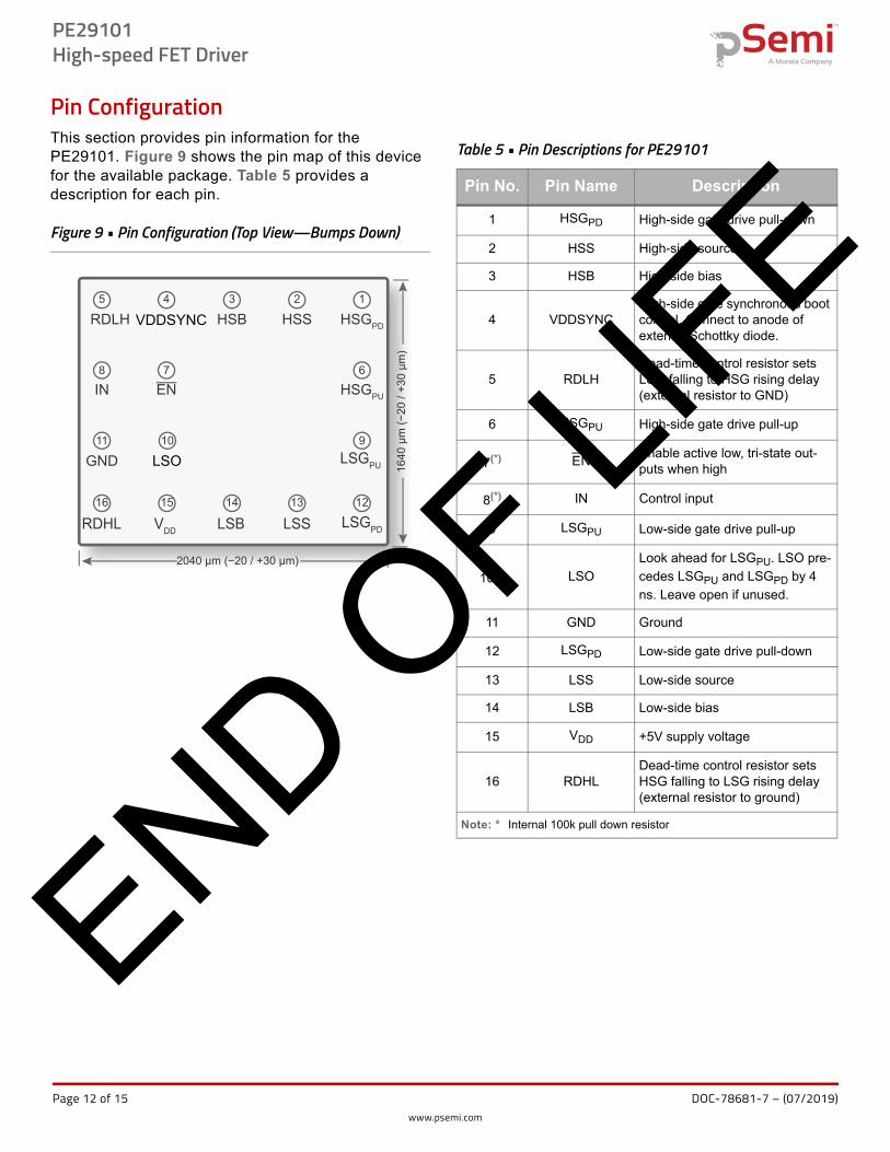
Pin ConfigurationThis section provides pin information for the PE29101. Figure 9 shows the pin map of this device for the available package. Table 5 provides a description for each pin.
Figure 9 • Pin Configuration (Top View—Bumps Down)
1640
µm
(−20
/ +3
0 µm
)
2040 µm (−20 / +30 µm)
HSSHSBRDLH
IN
GND
RDHL VDD LSB LSS LSGPD
HSGPUEN
HSGPD
1
6
9
1213141516
11
8
5 4 3 2
7
10LSGPU
VDDSYNC
LSO
Table 5 • Pin Descriptions for PE29101
Pin No. Pin Name Description
1 HSGPD High-side gate drive pull-down
2 HSS High-side source
3 HSB High-side bias
4 VDDSYNCHigh-side gate synchronous boot control. Connect to anode of external Schottky diode.
5 RDLHDead-time control resistor sets LSG falling to HSG rising delay (external resistor to GND)
6 HSGPU High-side gate drive pull-up
7(*) ENEnable active low, tri-state out-puts when high
8(*) IN Control input
9 LSGPU Low-side gate drive pull-up
10(*) LSO
Look ahead for LSGPU. LSO pre-
cedes LSGPU and LSGPD by 4
ns. Leave open if unused.
11 GND Ground
12 LSGPD Low-side gate drive pull-down
13 LSS Low-side source
14 LSB Low-side bias
15 VDD +5V supply voltage
16 RDHLDead-time control resistor sets HSG falling to LSG rising delay (external resistor to ground)
Note: * Internal 100k pull down resistor
END OF LI
FE
Page 12 of 15 DOC-78681-7 – (07/2019)www.psemi.com

PE29101High-speed FET Driver
Die Mechanical SpecificationsThis section provides the die mechanical specifications for the PE29101.
Table 6 • Die Mechanical Specifications for PE29101
Parameter Min Typ Max Unit Test Condition
Die size, singulated (x,y) 2040 × 1640 µmIncluding sapphire,
max tolerance = –20/+30
Wafer thickness 180 200 220 µm
Wafer size µm
Bump pitch 400 µm
Bump height 85 µm
Bump diameter 110 µm max tolerance = ±17
Figure 10 • Recommended Land Pattern for PE29101
BUMPS DOWN
SIDE VIEW
BUMPS UP
2.040+0.03-0.02
1.640+0.03-0.02
0.22(x14)
0.40
0.085±0.013
RECOMMENDED LAND PATTERN
0.40
0.20±0.02
Ø0.090±0.008(x16)Ø0.110±0.017
(x16)
END OF LI
FE
DOC-78681-7 – (07/2019) Page 13 of 15www.psemi.com
PE29101High-speed FET Driver
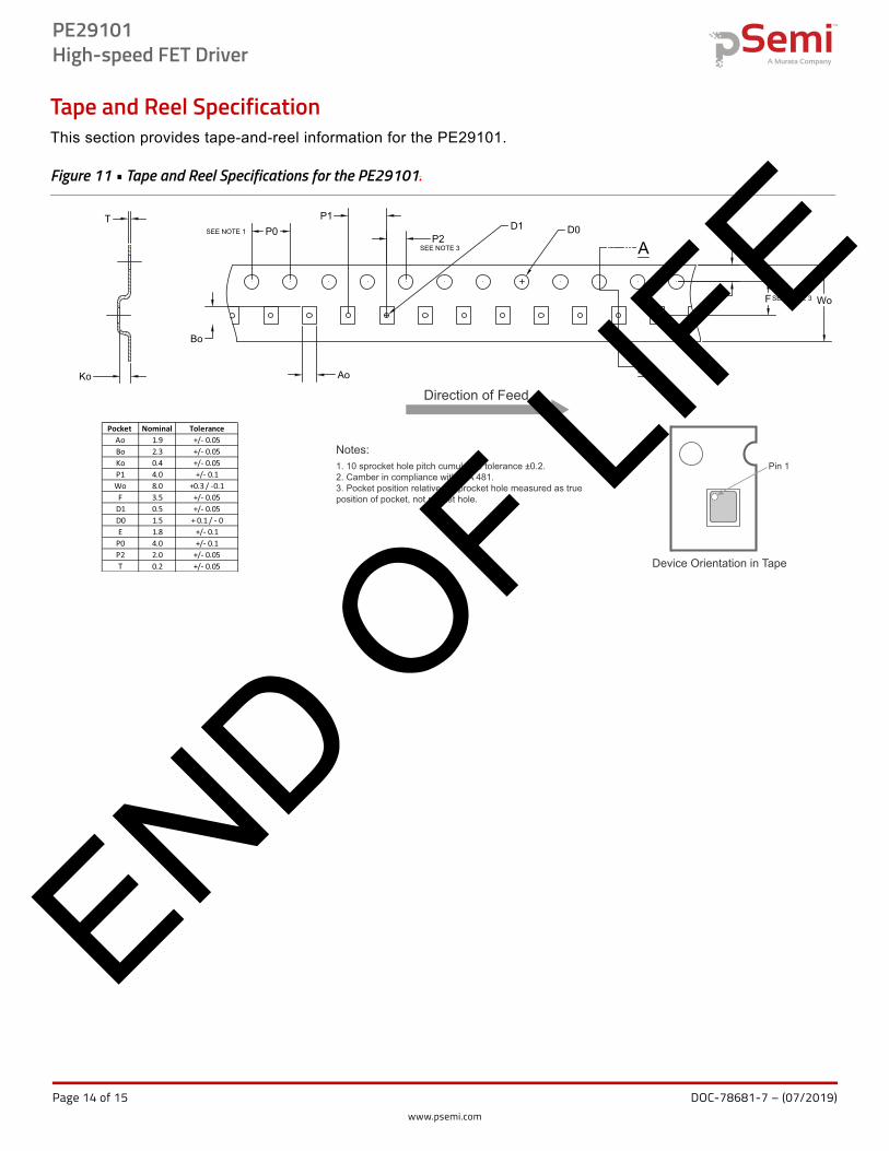
Tape and Reel SpecificationThis section provides tape-and-reel information for the PE29101.
Figure 11 • Tape and Reel Specifications for the PE29101.
Device Orientation in Tape
Pin 1
Notes:1. 10 sprocket hole pitch cumulative tolerance ±0.2.2. Camber in compliance with EIA 481.3. Pocket position relative to sprocket hole measured as true position of pocket, not pocket hole.
Direction of Feed
Bo
Ao
TD0D1
WoFE
P1P0
A
AP2
Ko
SEE NOTE 3
SEE NOTE 3
SEE NOTE 1
Pocket Nominal ToleranceAo 1.9 +/- 0.05Bo 2.3 +/- 0.05Ko 0.4 +/- 0.05P1 4.0 +/- 0.1Wo 8.0 +0.3 / -0.1
F 3.5 +/- 0.05D1 0.5 +/- 0.05D0 1.5 + 0.1 / - 0E 1.8 +/- 0.1
P0 4.0 +/- 0.1P2 2.0 +/- 0.05T 0.2 +/- 0.05
END OF LI
FE
Page 14 of 15 DOC-78681-7 – (07/2019)www.psemi.com

PE29101 High-speed FET Driver
Ordering InformationTable 7 lists the available ordering codes for the PE29101.
Table 7 • Order Codes for PE29101
Order Codes Description Packaging Shipping Method
PE29101A-X PE29101 flip chip Die on tape and reel 500 units/T&R
PE29101A-Z PE29101 flip chip Die on tape and reel 3000 units/T&R
LIFE
Product Specification www.psemi.com DOC-78681-7 – (07/2019)
Document CategoriesAdvance InformationThe product is in a formative or design stage. The datasheet contains design target specifications for product development. Specifications andfeatures may change in any manner without notice.
Preliminary SpecificationThe datasheet contains preliminary data. Additional data may be added at a later date. pSemi reserves the right to change specifications at anytime without notice in order to supply the best possible product.
Product SpecificationThe datasheet contains final data. In the event pSemi decides to change the specifications, pSemi will notify customers of the intended changes byissuing a CNF (Customer Notification Form).
Sales ContactFor additional information, contact Sales at [email protected].
DisclaimersThe information in this document is believed to be reliable. However, pSemi assumes no liability for the use of this information. Use shall be entirelyat the user’s own risk. No patent rights or licenses to any circuits described in this document are implied or granted to any third party. pSemi’sproducts are not designed or intended for use in devices or systems intended for surgical implant, or in other applications intended to support orsustain life, or in any application in which the failure of the pSemi product could create a situation in which personal injury or death might occur.pSemi assumes no liability for damages, including consequential or incidental damages, arising out of the use of its products in such applications.
Patent StatementpSemi products are protected under one or more of the following U.S. patents: patents.psemi.com
Copyright and Trademark©2018, pSemi Corporation. All rights reserved. The Peregrine Semiconductor name, Peregrine Semiconductor logo and UltraCMOS are registeredtrademarks and the pSemi name, pSemi logo, HaRP and DuNE are trademarks of pSemi Corporation in the U.S. and other countries.
END OF