Embed Size (px)
Citation preview
www.rohm.com TSZ02201-0RAR1G200270-1-2 © 2013 ROHM Co., Ltd. All rights reserved. 1/33 12.Sep.2013 Rev.001 TSZ22111・14・001
Datasheet
Operational Amplifiers
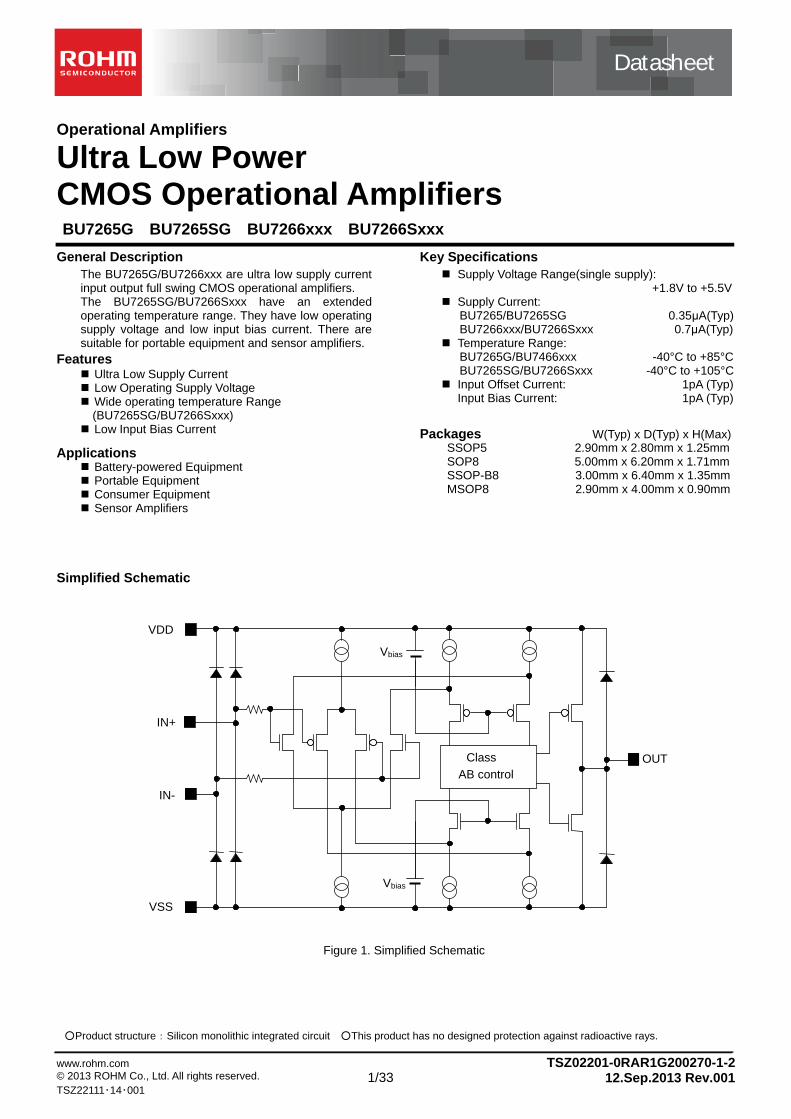
Ultra Low Power CMOS Operational Amplifiers BU7265G BU7265SG BU7266xxx BU7266Sxxx
General Description The BU7265G/BU7266xxx are ultra low supply current input output full swing CMOS operational amplifiers. The BU7265SG/BU7266Sxxx have an extended operating temperature range. They have low operating supply voltage and low input bias current. There are suitable for portable equipment and sensor amplifiers.
Features Ultra Low Supply Current Low Operating Supply Voltage Wide operating temperature Range
(BU7265SG/BU7266Sxxx) Low Input Bias Current
Applications
Battery-powered Equipment Portable Equipment Consumer Equipment Sensor Amplifiers
Key Specifications Supply Voltage Range(single supply): +1.8V to +5.5V Supply Current:
BU7265/BU7265SG 0.35μA(Typ) BU7266xxx/BU7266Sxxx t0.7μA(Typ)
Temperature Range: BU7265G/BU7466xxx ttt-40°C to +85°C
BU7265SG/BU7266Sxxx -40°C to +105°C Input Offset Current: 1pA (Typ)
Input Bias Current: 1pA (Typ) Packages jW(Typ) x D(Typ) x H(Max)
SSOP5 M-B2.90mm x 2.80mm x 1.25mm SOP8 jMS-jj5.00mm x 6.20mm x 1.71mm SSOP-B8 5M3.00mm x 6.40mm x 1.35mm MSOP8 -5SB2.90mm x 4.00mm x 0.90mm
Simplified Schematic
Figure 1. Simplified Schematic
Product structure:Silicon monolithic integrated circuit This product has no designed protection against radioactive rays.
IN+
OUT
IN-
VDD
VSS
Vbias
Class
AB control
Vbias
Datasheet
www.rohm.com TSZ02201-0RAR1G200270-1-2 © 2013 ROHM Co., Ltd. All rights reserved. 2/33 12.Sep.2013 Rev.001 TSZ22111・15・001
BU7265G BU7265SG BU7266xxx BU7266Sxxx
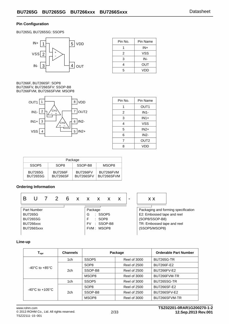
Pin Configuration BU7265G, BU7265SG: SSOP5
Pin No. Pin Name
1 IN+
2 VSS
3 IN-
4 OUT
5 VDD
BU7266F, BU7266SF: SOP8 BU7266FV, BU7266SFV: SSOP-B8 BU7266FVM, BU7266SFVM: MSOP8
Pin No. Pin Name
1 OUT1
2 IN1-
3 IN1+
4 VSS
5 IN2+
6 IN2-
7 OUT2
8 VDD
Package
SSOP5 SOP8 SSOP-B8 MSOP8
BU7265G BU7265SG
BU7266F BU7266SF
BU7266FV BU7266SFV
BU7266FVMBU7266SFVM
Ordering Information
B U 7 2 6 x x x x x - x x
Part Number BU7265G BU7265SG BU7266xxx BU7266Sxxx
Package G : SSOP5 F : SOP8 FV : SSOP-B8 FVM : MSOP8
Packaging and forming specification E2: Embossed tape and reel (SOP8/SSOP-B8) TR: Embossed tape and reel (SSOP5/MSOP8)
Line-up
Topr Channels Package Orderable Part Number
-40°C to +85°C
1ch SSOP5 Reel of 3000 BU7265G-TR
2ch
SOP8 Reel of 2500 BU7266F-E2
SSOP-B8 Reel of 2500 BU7266FV-E2
MSOP8 Reel of 3000 BU7266FVM-TR
-40°C to +105°C
1ch SSOP5 Reel of 3000 BU7265SG-TR
2ch
SOP8 Reel of 2500 BU7266SF-E2
SSOP-B8 Reel of 2500 BU7266SFV-E2
MSOP8 Reel of 3000 BU7266SFVM-TR
3 4
2
1 5
+-
OUT
IN+
IN-
VSS
VDD
- +
+ -
CH1
CH2
81
2
3
4 5
6
7
OUT1
-IN1
+IN1
VEE
VCC
OUT2
-IN2
+IN2
VDD
OUT2
IN2-
IN2+
OUT1
IN1-
IN1+
VSS
Datasheet
www.rohm.com TSZ02201-0RAR1G200270-1-2 © 2013 ROHM Co., Ltd. All rights reserved. 3/33 12.Sep.2013 Rev.001 TSZ22111・15・001
BU7265G BU7265SG BU7266xxx BU7266Sxxx
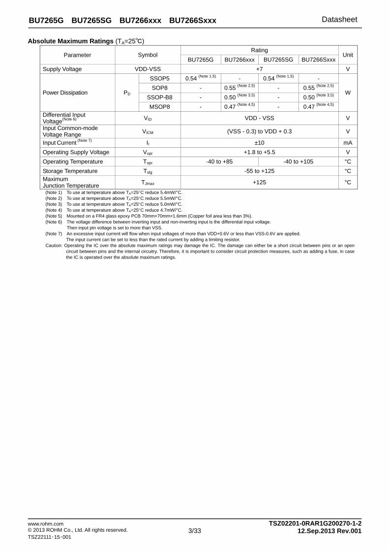
Absolute Maximum Ratings (TA=25)
Parameter Symbol Rating
UnitBU7265G BU7266xxx BU7265SG BU7266Sxxx
Supply Voltage VDD-VSS +7 V
Power Dissipation PD
SSOP5 0.54 (Note 1,5) - 0.54 (Note 1,5) -
W SOP8 - 0.55 (Note 2,5) - 0.55 (Note 2,5)
SSOP-B8 - 0.50 (Note 3,5) - 0.50 (Note 3,5)
MSOP8 - 0.47 (Note 4,5) - 0.47 (Note 4,5)
Differential Input Voltage(Note 6)
VID VDD - VSS V
Input Common-mode Voltage Range VICM (VSS - 0.3) to VDD + 0.3 V
Input Current (Note 7) II ±10 mA
Operating Supply Voltage Vopr +1.8 to +5.5 V
Operating Temperature Topr -40 to +85 -40 to +105 °C
Storage Temperature Tstg -55 to +125 °C Maximum Junction Temperature
TJmax +125 °C
(Note 1) To use at temperature above TA=25C reduce 5.4mW/°C. (Note 2) To use at temperature above TA=25C reduce 5.5mW/°C. (Note 3) To use at temperature above TA=25C reduce 5.0mW/°C. (Note 4) To use at temperature above TA=25C reduce 4.7mW/°C. (Note 5) Mounted on a FR4 glass epoxy PCB 70mm×70mm×1.6mm (Copper foil area less than 3%). (Note 6) The voltage difference between inverting input and non-inverting input is the differential input voltage. Then input pin voltage is set to more than VSS. (Note 7) An excessive input current will flow when input voltages of more than VDD+0.6V or less than VSS-0.6V are applied. The input current can be set to less than the rated current by adding a limiting resistor. Caution: Operating the IC over the absolute maximum ratings may damage the IC. The damage can either be a short circuit between pins or an open
circuit between pins and the internal circuitry. Therefore, it is important to consider circuit protection measures, such as adding a fuse, in case the IC is operated over the absolute maximum ratings.
Datasheet
www.rohm.com TSZ02201-0RAR1G200270-1-2 © 2013 ROHM Co., Ltd. All rights reserved. 4/33 12.Sep.2013 Rev.001 TSZ22111・15・001
BU7265G BU7265SG BU7266xxx BU7266Sxxx
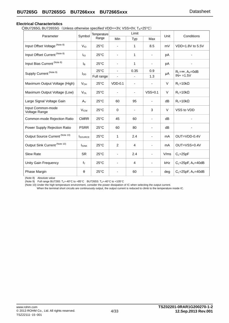
Electrical Characteristics BU7265G, BU7265SG(Unless otherwise specified VDD=+3V, VSS=0V, TA=25°C)
Parameter Symbol Temperature
Range Limit
Unit Conditions Min Typ Max
Input Offset Voltage (Note 8) VIO 25°C - 1 8.5 mV VDD=1.8V to 5.5V
Input Offset Current (Note 8) IIO 25°C - 1 - pA -
Input Bias Current (Note 8) IB 25°C - 1 - pA -
Supply Current (Note 9) IDD 25°C - 0.35 0.9
μA RL=∞, AV=0dB IN+ =1.5V Full range - - 1.3
Maximum Output Voltage (High) VOH 25°C VDD-0.1 - - V RL=10kΩ
Maximum Output Voltage (Low) VOL 25°C - - VSS+0.1 V RL=10kΩ
Large Signal Voltage Gain AV 25°C 60 95 - dB RL=10kΩ
Input Common-mode Voltage Range VICM 25°C 0 - 3 V VSS to VDD
Common-mode Rejection Ratio CMRR 25°C 45 60 - dB -
Power Supply Rejection Ratio PSRR 25°C 60 80 - dB -
Output Source Current (Note 10) ISOURCE 25°C 1 2.4 - mA OUT=VDD-0.4V
Output Sink Current (Note 10) ISINK 25°C 2 4 - mA OUT=VSS+0.4V
Slew Rate SR 25°C - 2.4 - V/ms CL=25pF
Unity Gain Frequency fT 25°C - 4 - kHz CL=25pF, AV=40dB
Phase Margin θ 25°C - 60 - deg CL=25pF, AV=40dB
(Note 8) Absolute value (Note 9) Full range BU7265: TA=-40C to +85C BU7265S: TA=-40C to +105C (Note 10) Under the high temperature environment, consider the power dissipation of IC when selecting the output current. When the terminal short circuits are continuously output, the output current is reduced to climb to the temperature inside IC.
Datasheet
www.rohm.com TSZ02201-0RAR1G200270-1-2 © 2013 ROHM Co., Ltd. All rights reserved. 5/33 12.Sep.2013 Rev.001 TSZ22111・15・001
BU7265G BU7265SG BU7266xxx BU7266Sxxx
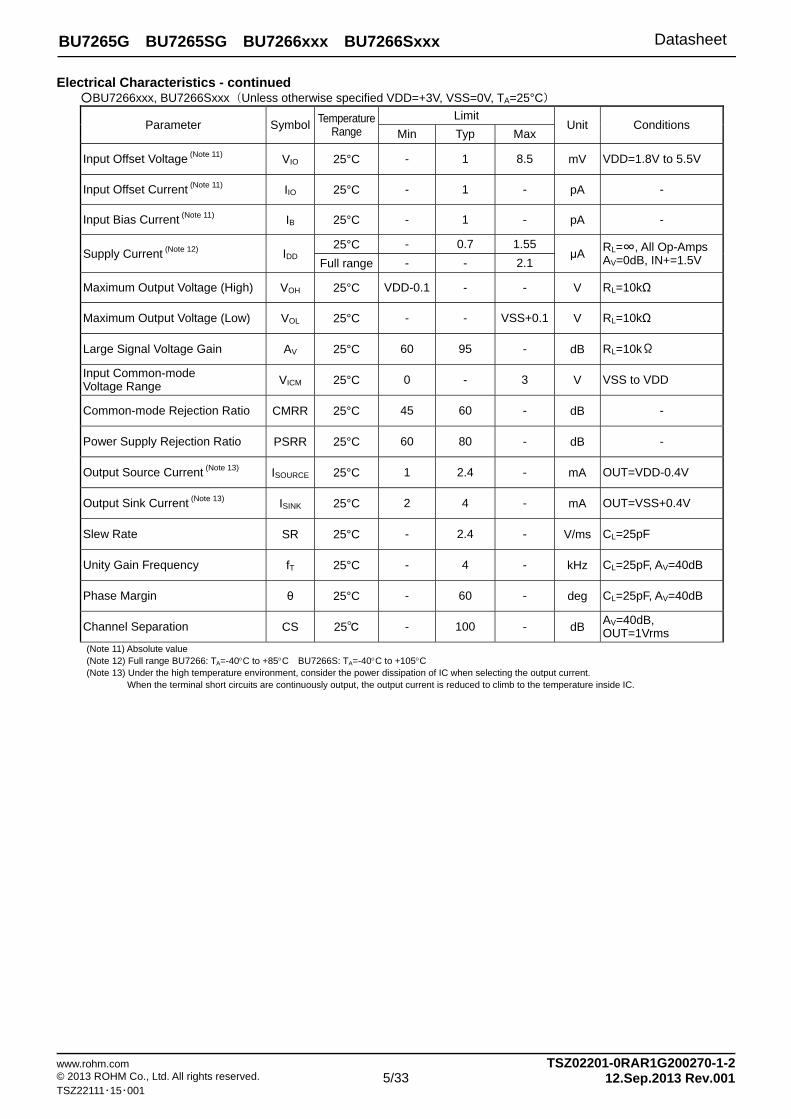
Electrical Characteristics - continued BU7266xxx, BU7266Sxxx(Unless otherwise specified VDD=+3V, VSS=0V, TA=25°C)
Parameter Symbol TemperatureRange
Limit Unit Conditions
Min Typ Max
Input Offset Voltage (Note 11) VIO 25°C - 1 8.5 mV VDD=1.8V to 5.5V
Input Offset Current (Note 11) IIO 25°C - 1 - pA -
Input Bias Current (Note 11) IB 25°C - 1 - pA -
Supply Current (Note 12) IDD
25°C - 0.7 1.55 μA
RL=∞, All Op-Amps AV=0dB, IN+=1.5V Full range - - 2.1
Maximum Output Voltage (High) VOH 25°C VDD-0.1 - - V RL=10kΩ
Maximum Output Voltage (Low) VOL 25°C - - VSS+0.1 V RL=10kΩ
Large Signal Voltage Gain AV 25°C 60 95 - dB RL=10kΩ
Input Common-mode Voltage Range VICM 25°C 0 - 3 V VSS to VDD
Common-mode Rejection Ratio CMRR 25°C 45 60 - dB -
Power Supply Rejection Ratio PSRR 25°C 60 80 - dB -
Output Source Current (Note 13) ISOURCE 25°C 1 2.4 - mA OUT=VDD-0.4V
Output Sink Current (Note 13) ISINK 25°C 2 4 - mA OUT=VSS+0.4V
Slew Rate SR 25°C - 2.4 - V/ms CL=25pF
Unity Gain Frequency fT 25°C - 4 - kHz CL=25pF, AV=40dB
Phase Margin θ 25°C - 60 - deg CL=25pF, AV=40dB
Channel Separation CS 25 - 100 - dB AV=40dB, OUT=1Vrms
(Note 11) Absolute value (Note 12) Full range BU7266: TA=-40C to +85C BU7266S: TA=-40C to +105C (Note 13) Under the high temperature environment, consider the power dissipation of IC when selecting the output current. When the terminal short circuits are continuously output, the output current is reduced to climb to the temperature inside IC.
Datasheet
www.rohm.com TSZ02201-0RAR1G200270-1-2 © 2013 ROHM Co., Ltd. All rights reserved. 6/33 12.Sep.2013 Rev.001 TSZ22111・15・001
BU7265G BU7265SG BU7266xxx BU7266Sxxx
Description of Electrical Characteristics Described below are descriptions of the relevant electrical terms used in this datasheet. Items and symbols used are also shown. Note that item name and symbol and their meaning may differ from those on another manufacturer’s document or general document. 1. Absolute maximum ratings
Absolute maximum rating items indicate the condition which must not be exceeded. Application of voltage in excess of absolute maximum rating or use out of absolute maximum rated temperature environment may cause deterioration of characteristics. (1) Supply Voltage (VDD/VSS)
Indicates the maximum voltage that can be applied between the VDD terminal and VSS terminal without deterioration or destruction of characteristics of internal circuit.
(2) Differential Input Voltage (VID) Indicates the maximum voltage that can be applied between non-inverting and inverting terminals without damaging the IC.
(3) Input Common-mode Voltage Range (VICM) Indicates the maximum voltage that can be applied to the non-inverting and inverting terminals without deterioration or destruction of electrical characteristics. Input common-mode voltage range of the maximum ratings does not assure normal operation of IC. For normal operation, use the IC within the input common-mode voltage range characteristics.
(4) Power Dissipation (PD) Indicates the power that can be consumed by the IC when mounted on a specific board at the ambient temperature 25(normal temperature). As for package product, PD is determined by the temperature that can be permitted by the IC in the package (maximum junction temperature) and the thermal resistance of the package.
2. Electrical characteristics
(1) Input Offset Voltage (VIO) Indicates the voltage difference between non-inverting terminal and inverting terminals. It can be translated into the input voltage difference required for setting the output voltage at 0 V.
(2) Input Offset Current (IIO) Indicates the difference of input bias current between the non-inverting and inverting terminals.
(3) Input Bias Current (IB) Indicates the current that flows into or out of the input terminal. It is defined by the average of input bias currents at the non-inverting and inverting terminals.
(4) Supply Current (IDD) Indicates the current that flows within the IC under specified no-load conditions.
(5) Maximum Output Voltage(High) / Maximum Output Voltage(Low) (VOH/VOL) Indicates the voltage range of the output under specified load condition. It is typically divided into maximum output voltage High and low. Maximum output voltage high indicates the upper limit of output voltage. Maximum output voltage low indicates the lower limit.
(6) Large Signal Voltage Gain (AV) Indicates the amplifying rate (gain) of output voltage against the voltage difference between non-inverting terminal and inverting terminal. It is normally the amplifying rate (gain) with reference to DC voltage. Av = (Output voltage) / (Differential Input voltage)
(7) Input Common-mode Voltage Range (VICM) Indicates the input voltage range where IC normally operates.
(8) Common-mode Rejection Ratio (CMRR) Indicates the ratio of fluctuation of input offset voltage when the input common mode voltage is changed. It is normally the fluctuation of DC. CMRR = (Change of Input common-mode voltage)/(Input offset fluctuation)
(9) Power Supply Rejection Ratio (PSRR) Indicates the ratio of fluctuation of input offset voltage when supply voltage is changed. It is normally the fluctuation of DC. PSRR= (Change of power supply voltage)/(Input offset fluctuation)
(10) Output Source Current/ Output Sink Current (ISOURCE / ISINK) The maximum current that can be output from the IC under specific output conditions. The output source current indicates the current flowing out from the IC, and the output sink current indicates the current flowing into the IC.
(11) Slew Rate (SR) Indicates the ratio of the change in output voltage with time when a step input signal is applied.
(12) Unity Gain Frequency (fT) Indicates a frequency where the voltage gain of operational amplifier is 1.
(13) Phase Margin (θ) Indicates the margin of phase from 180 degree phase lag at unity gain frequency.
(14) Channel Separation (CS) Indicates the fluctuation in the output voltage of the driven channel with reference to the change of output voltage of the channel which is not driven.
Datasheet
www.rohm.com TSZ02201-0RAR1G200270-1-2 © 2013 ROHM Co., Ltd. All rights reserved. 7/33 12.Sep.2013 Rev.001 TSZ22111・15・001
BU7265G BU7265SG BU7266xxx BU7266Sxxx
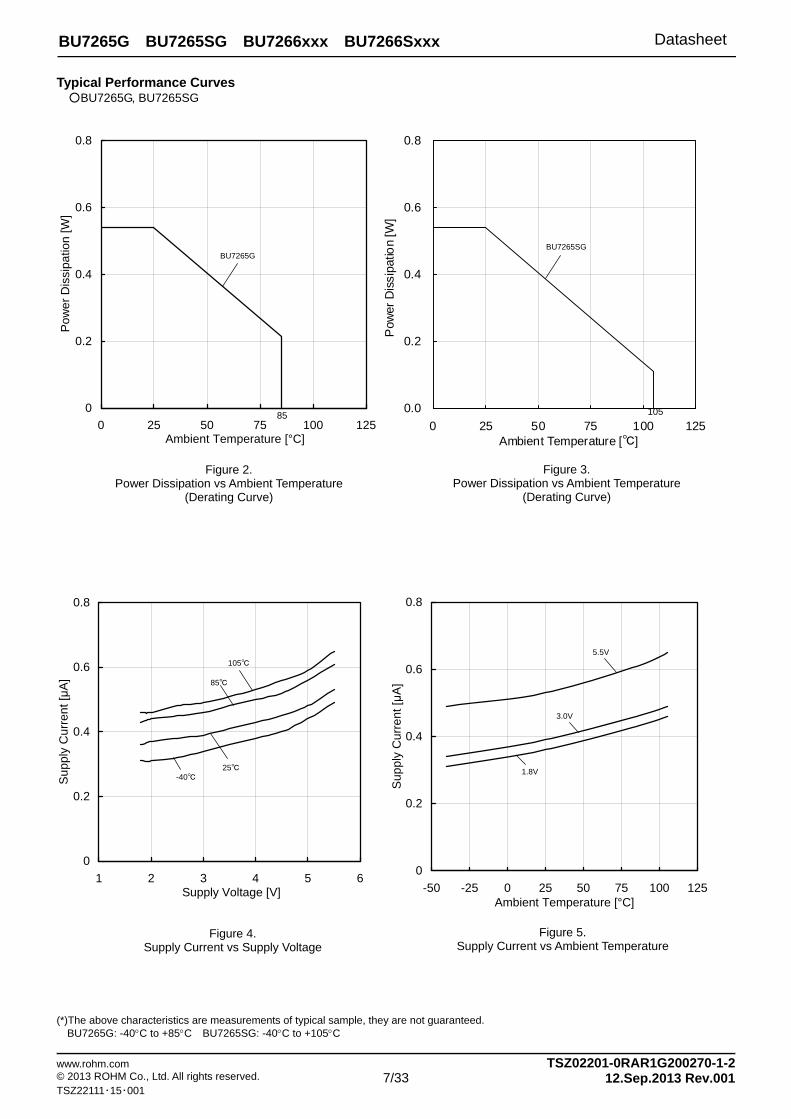
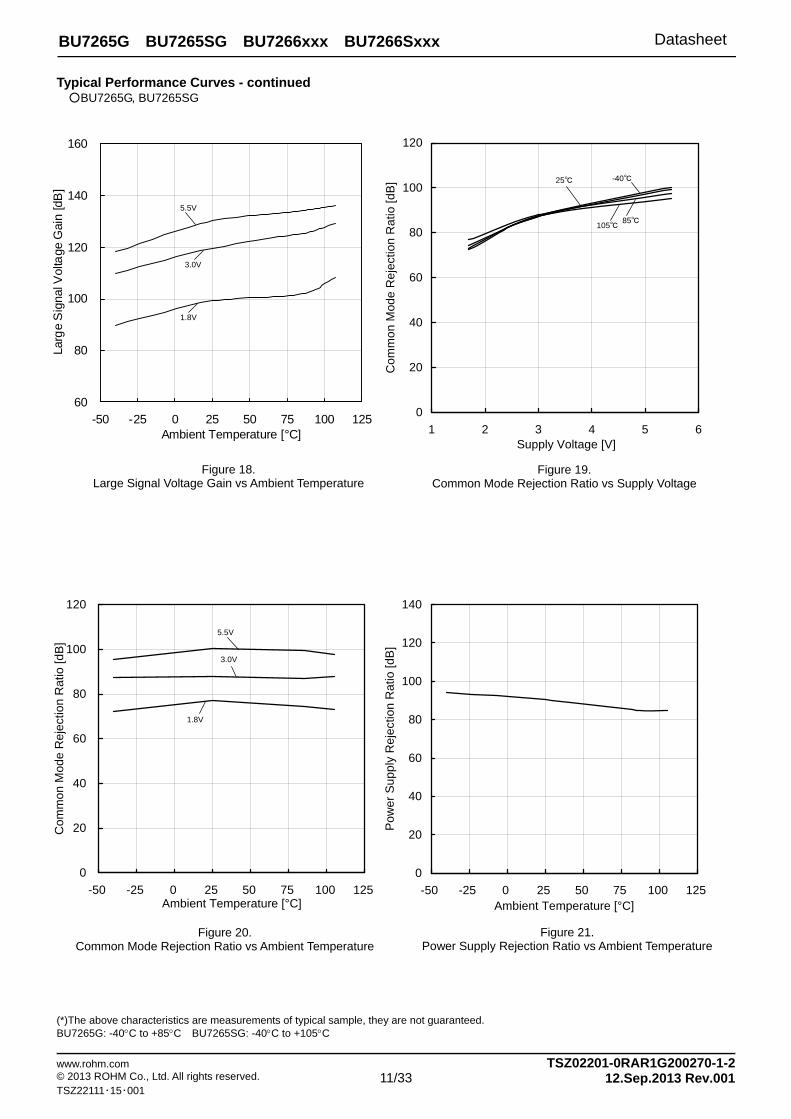
Typical Performance Curves BU7265G, BU7265SG
(*)The above characteristics are measurements of typical sample, they are not guaranteed. BU7265G: -40C to +85C BU7265SG: -40C to +105C
Figure 2. Power Dissipation vs Ambient Temperature
(Derating Curve)
Figure 3. Power Dissipation vs Ambient Temperature
(Derating Curve)
Figure 4. Supply Current vs Supply Voltage
Figure 5. Supply Current vs Ambient Temperature
0
0.2
0.4
0.6
0.8
1 2 3 4 5 6Supply Voltage [V]
Su
pply
Cur
ren
t [μ
A]
-40 25
85
105
0
0.2
0.4
0.6
0.8
-50 -25 0 25 50 75 100 125Ambient Temperature [°C]
Su
pp
ly C
urr
en
t [μ
A]
1.8V
5.5V
3.0V
0
0.2
0.4
0.6
0.8
0 25 50 75 100 125Ambient Temperature [°C]
Po
we
r D
issi
patio
n [
W]
BU7265G
85
BU7265SG
105 0.0
0.2
0.4
0.6
0.8
0 25 50 75 100 125Ambient Temperature []
Pow
er D
issi
patio
n [W
] .
Datasheet
www.rohm.com TSZ02201-0RAR1G200270-1-2 © 2013 ROHM Co., Ltd. All rights reserved. 8/33 12.Sep.2013 Rev.001 TSZ22111・15・001
BU7265G BU7265SG BU7266xxx BU7266Sxxx
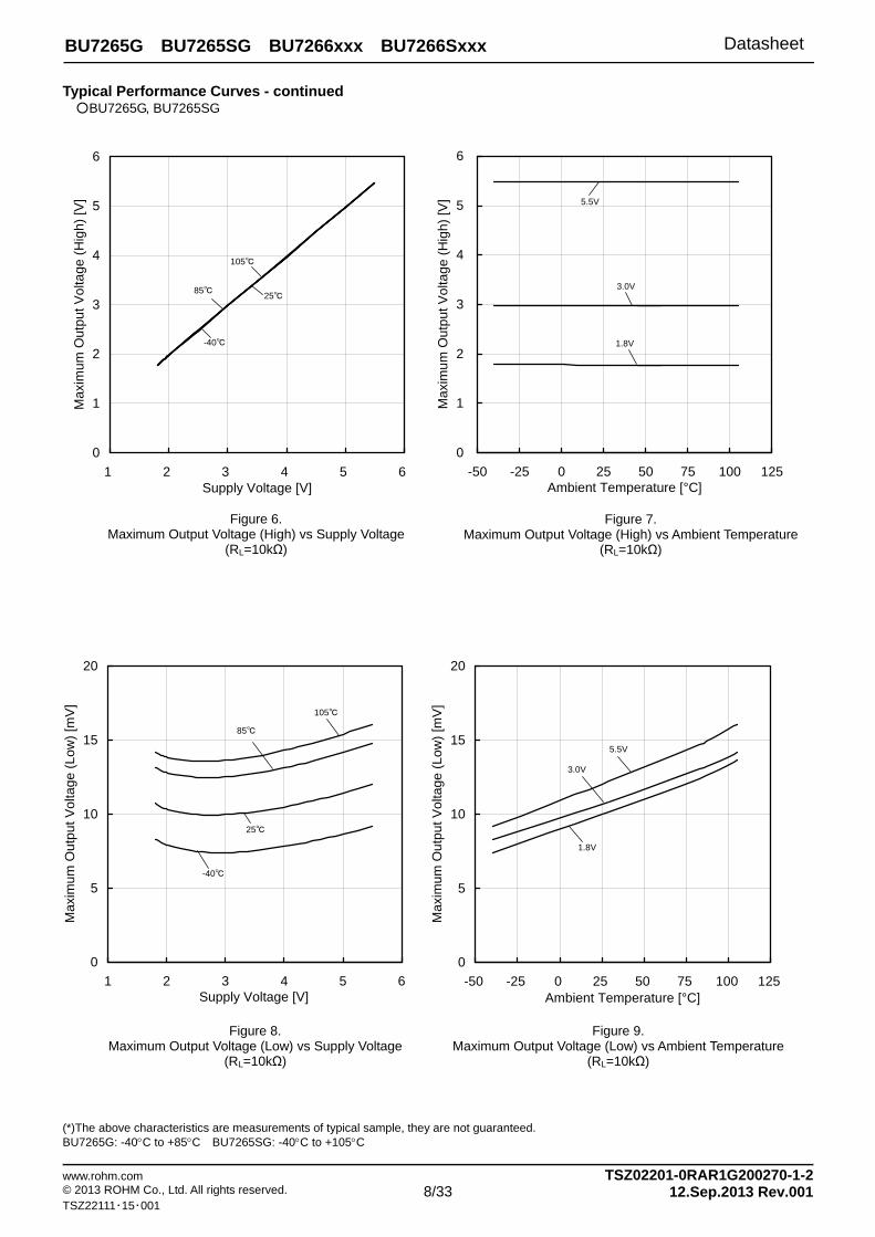
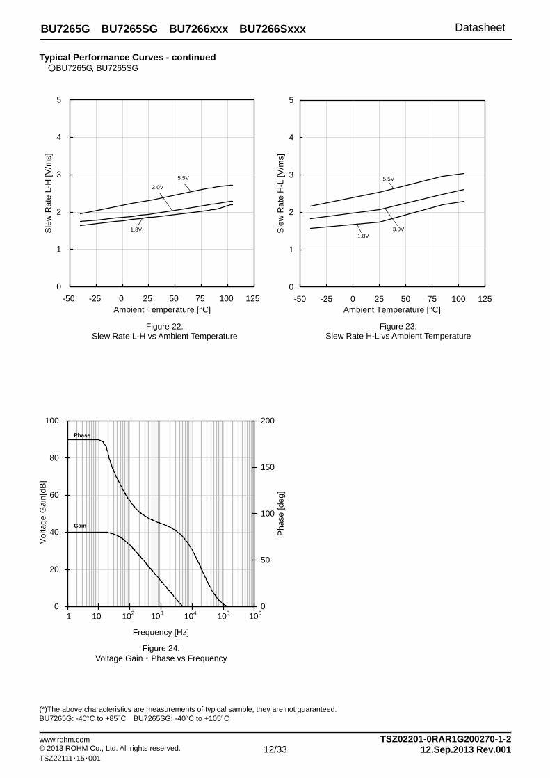
Typical Performance Curves - continued BU7265G, BU7265SG
(*)The above characteristics are measurements of typical sample, they are not guaranteed. BU7265G: -40C to +85C BU7265SG: -40C to +105C
0
1
2
3
4
5
6
1 2 3 4 5 6Supply Voltage [V]
Max
imum
Out
put
Vol
tage
(H
igh
) [V
]
0
5
10
15
20
1 2 3 4 5 6Supply Voltage [V]
Ma
xim
um
Ou
tpu
t V
olta
ge
(L
ow
) [m
V]
0
1
2
3
4
5
6
-50 -25 0 25 50 75 100 125Ambient Temperature [°C]
Ma
xim
um
Ou
tpu
t Vo
ltag
e (
Hig
h)
[V]
0
5
10
15
20
-50 -25 0 25 50 75 100 125Ambient Temperature [°C]
Ma
xim
um
Ou
tpu
t Vo
ltag
e (
Low
) [m
V]
Figure 8. Maximum Output Voltage (Low) vs Supply Voltage
(RL=10kΩ)
Figure 6. Maximum Output Voltage (High) vs Supply Voltage
(RL=10kΩ)
Figure 7. Maximum Output Voltage (High) vs Ambient Temperature
(RL=10kΩ)
Figure 9. Maximum Output Voltage (Low) vs Ambient Temperature
(RL=10kΩ)
-40
25 85
105
1.8V
5.5V
3.0V
-40
25
85
105
1.8V
5.5V
3.0V
Datasheet
www.rohm.com TSZ02201-0RAR1G200270-1-2 © 2013 ROHM Co., Ltd. All rights reserved. 9/33 12.Sep.2013 Rev.001 TSZ22111・15・001
BU7265G BU7265SG BU7266xxx BU7266Sxxx
Figure 11. Output Source Current vs Ambient Temperature
(OUT=VDD-0.4V)
Typical Performance Curves - continued BU7265G, BU7265SG
(*)The above characteristics are measurements of typical sample, they are not guaranteed. BU7265G: -40C to +85C BU7265SG: -40C to +105C
0
2
4
6
8
10
-50 -25 0 25 50 75 100 125Ambient Temperature [°C]
Ou
tpu
t S
ou
rce
Cu
rre
nt
[mA
]0
2
4
6
8
10
0.0 0.5 1.0 1.5 2.0 2.5 3.0Output Voltage [V]
Ou
tpu
t S
ou
rce
Cu
rre
nt
[mA
]
0
5
10
15
20
-50 -25 0 25 50 75 100 125Ambient Temperature [°C]
Ou
tpu
t S
ink
Cur
ren
t [m
A]
0
5
10
15
20
0.0 0.5 1.0 1.5 2.0 2.5 3.0
Output Voltage [V]
Ou
tpu
t S
ink
Cu
rre
nt
[mA
]
Figure 13. Output Sink Current vs Ambient Temperature
(OUT=VSS+0.4V)
Figure 12. Output Sink Current vs Output Voltage
(VDD=3V)
Figure 10. Output Source Current vs Output Voltage
(VDD=3 V)
-40
1.8V
5.5V
3.0V
-40
25
85
105 5.5V
1.8V
3.0V
25
85
105
Datasheet
www.rohm.com TSZ02201-0RAR1G200270-1-2 © 2013 ROHM Co., Ltd. All rights reserved. 10/33 12.Sep.2013 Rev.001 TSZ22111・15・001
BU7265G BU7265SG BU7266xxx BU7266Sxxx
Typical Performance Curves - continued BU7265G, BU7265SG
(*)The above characteristics are measurements of typical sample, they are not guaranteed. BU7265G: -40C to +85C BU7265SG: -40C to +105C
-10.0
-7.5
-5.0
-2.5
0.0
2.5
5.0
7.5
10.0
1 2 3 4 5 6
Supply Voltage [V]
Inp
ut O
ffse
t Vo
ltag
e [m
V]
-10.0
-7.5
-5.0
-2.5
0.0
2.5
5.0
7.5
10.0
-50 -25 0 25 50 75 100 125Ambient Temperature [°C]
Inp
ut
Off
set
Vo
ltag
e [
mV
]
-10.0
-7.5
-5.0
-2.5
0.0
2.5
5.0
7.5
10.0
-1 0 1 2 3 4Input Voltage [V]
Inp
ut O
ffse
t V
olta
ge
[m
V]
60
80
100
120
140
160
1 2 3 4 5 6Supply Voltage [V]
Larg
e S
igna
l Vol
tage
Gai
n [d
B]
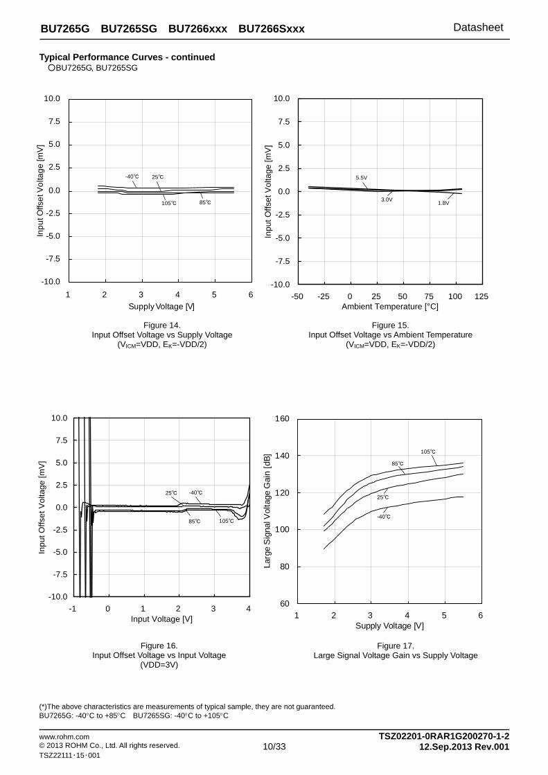
Figure 14. Input Offset Voltage vs Supply Voltage
(VICM=VDD, EK=-VDD/2)
Figure 15. Input Offset Voltage vs Ambient Temperature
(VICM=VDD, EK=-VDD/2)
Figure 16. Input Offset Voltage vs Input Voltage
(VDD=3V)
Figure 17. Large Signal Voltage Gain vs Supply Voltage
-40 25
85 105
5.5V
1.8V 3.0V
-40 25
25
85
105
-40 85 105
Datasheet
www.rohm.com TSZ02201-0RAR1G200270-1-2 © 2013 ROHM Co., Ltd. All rights reserved. 11/33 12.Sep.2013 Rev.001 TSZ22111・15・001
BU7265G BU7265SG BU7266xxx BU7266Sxxx
Typical Performance Curves - continued BU7265G, BU7265SG
(*)The above characteristics are measurements of typical sample, they are not guaranteed. BU7265G: -40C to +85C BU7265SG: -40C to +105C
60
80
100
120
140
160
-50 -25 0 25 50 75 100 125Ambient Temperature [°C]
Larg
e S
igna
l Vol
tage
Gai
n [d
B]
0
20
40
60
80
100
120
1 2 3 4 5 6Supply Voltage [V]
Co
mm
on
Mod
e R
eje
ctio
n R
atio
[d
B]
0
20
40
60
80
100
120
-50 -25 0 25 50 75 100 125Ambient Temperature [°C]
Co
mm
on
Mo
de
Re
ject
ion
Ra
tio [
dB
]
0
20
40
60
80
100
120
140
-50 -25 0 25 50 75 100 125Ambient Temperature [°C]
Po
we
r S
upp
ly R
eje
ctio
n R
atio
[dB
]
Figure 18. Large Signal Voltage Gain vs Ambient Temperature
Figure 19. Common Mode Rejection Ratio vs Supply Voltage
Figure 20. Common Mode Rejection Ratio vs Ambient Temperature
Figure 21. Power Supply Rejection Ratio vs Ambient Temperature
5.5V
1.8V
3.0V
-40 25
85 105
5.5V
1.8V
3.0V
Datasheet
www.rohm.com TSZ02201-0RAR1G200270-1-2 © 2013 ROHM Co., Ltd. All rights reserved. 12/33 12.Sep.2013 Rev.001 TSZ22111・15・001
BU7265G BU7265SG BU7266xxx BU7266Sxxx
Typical Performance Curves - continued BU7265G, BU7265SG
(*)The above characteristics are measurements of typical sample, they are not guaranteed. BU7265G: -40C to +85C BU7265SG: -40C to +105C
0
1
2
3
4
5
-50 -25 0 25 50 75 100 125Ambient Temperature [°C]
Sle
w R
ate
L-H
[V
/ms]
0
1
2
3
4
5
-50 -25 0 25 50 75 100 125Ambient Temperature [°C]
Sle
w R
ate
H-L
[V
/ms]
0
20
40
60
80
100
1.E+00 1.E+01 1.E+02 1.E+03 1.E+04 1.E+05 1.E+06
Frequency [Hz]
Vo
ltag
e G
ain
[dB
]
0
50
100
150
200
Ph
ase
[d
eg
]
Figure 22. Slew Rate L-H vs Ambient Temperature
Figure 23. Slew Rate H-L vs Ambient Temperature
Figure 24. Voltage Gain・Phase vs Frequency
5.5V
1.8V
3.0V
5.5V
1.8V 3.0V
Phase
Gain
1 10 102 103 104 105 106
Datasheet
www.rohm.com TSZ02201-0RAR1G200270-1-2 © 2013 ROHM Co., Ltd. All rights reserved. 13/33 12.Sep.2013 Rev.001 TSZ22111・15・001
BU7265G BU7265SG BU7266xxx BU7266Sxxx
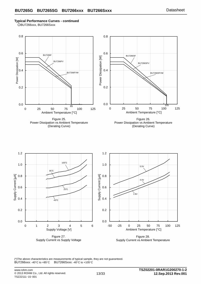
Typical Performance Curves - continued BU7266xxx, BU7266Sxxx
(*)The above characteristics are measurements of typical sample, they are not guaranteed. BU7266xxx: -40C to +85C BU7266Sxxx: -40C to +105C
0.0
0.2
0.4
0.6
0.8
0 25 50 75 100 125Ambient Temperature [°C]
Pow
er D
issi
patio
n [W
]
0.0
0.2
0.4
0.6
0.8
1.0
1.2
0 1 2 3 4 5 6Supply Voltage [V]
Su
pp
ly C
urr
en
t [μ
A]
0.0
0.2
0.4
0.6
0.8
1.0
1.2
-50 -25 0 25 50 75 100 125Ambient Temperature [°C]
Su
ppl
y C
urre
nt [μ
A]
Figure 25. Power Dissipation vs Ambient Temperature
(Derating Curve)
Figure 26. Power Dissipation vs Ambient Temperature
(Derating Curve)
Figure 27. Supply Current vs Supply Voltage
Figure 28. Supply Current vs Ambient Temperature
BU7266F
BU7266FV
BU7266FVM
0.0
0.2
0.4
0.6
0.8
0 25 50 75 100 125Ambient Temperature [°C]
Pow
er D
issi
patio
n [
W] BU7266SF
BU7266SFV
BU7266SFVM
-40
25
85
105
1.8V
5.5V
3.0V
85 105
Datasheet
www.rohm.com TSZ02201-0RAR1G200270-1-2 © 2013 ROHM Co., Ltd. All rights reserved. 14/33 12.Sep.2013 Rev.001 TSZ22111・15・001
BU7265G BU7265SG BU7266xxx BU7266Sxxx
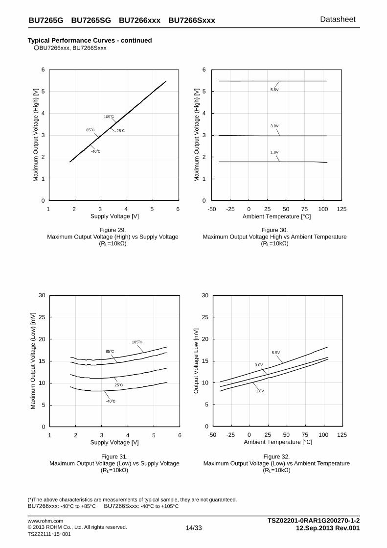
Typical Performance Curves - continued BU7266xxx, BU7266Sxxx
(*)The above characteristics are measurements of typical sample, they are not guaranteed. BU7266xxx: -40C to +85C BU7266Sxxx: -40C to +105C
0
1
2
3
4
5
6
1 2 3 4 5 6Supply Voltage [V]
Ma
xim
um
Ou
tpu
t V
olta
ge
(H
igh
) [V
]
0
1
2
3
4
5
6
-50 -25 0 25 50 75 100 125Ambient Temperature [°C]
Ma
xim
um
Ou
tpu
t V
olta
ge
(H
igh
) [V
]
0
5
10
15
20
25
30
1 2 3 4 5 6Supply Voltage [V]
Ma
xim
um
Ou
tpu
t V
olta
ge
(L
ow
) [m
V]
0
5
10
15
20
25
30
-50 -25 0 25 50 75 100 125Ambient Temperature [°C]
Ou
tpu
t Vo
ltag
e L
ow
[mV
]
Figure 29. Maximum Output Voltage (High) vs Supply Voltage
(RL=10kΩ)
Figure 30. Maximum Output Voltage High vs Ambient Temperature
(RL=10kΩ)
Figure 31. Maximum Output Voltage (Low) vs Supply Voltage
(RL=10kΩ)
Figure 32. Maximum Output Voltage (Low) vs Ambient Temperature
(RL=10kΩ)
-40
25 85
105
1.8V
5.5V
3.0V
-40
25
85
105
1.8V
5.5V
3.0V
Datasheet
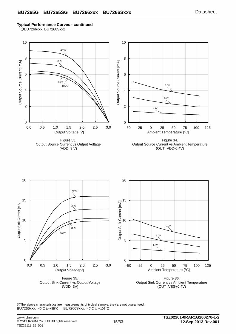
www.rohm.com TSZ02201-0RAR1G200270-1-2 © 2013 ROHM Co., Ltd. All rights reserved. 15/33 12.Sep.2013 Rev.001 TSZ22111・15・001
BU7265G BU7265SG BU7266xxx BU7266Sxxx
Figure 34. Output Source Current vs Ambient Temperature
(OUT=VDD-0.4V)
Typical Performance Curves - continued BU7266xxx, BU7266Sxxx
(*)The above characteristics are measurements of typical sample, they are not guaranteed. BU7266xxx: -40C to +85C BU7266Sxxx: -40C to +105C
0
2
4
6
8
10
0.0 0.5 1.0 1.5 2.0 2.5 3.0Output Voltage [V]
Ou
tpu
t S
ou
rce
Cu
rre
nt
[mA
]
0
2
4
6
8
10
-50 -25 0 25 50 75 100 125Ambient Temperature [°C]
Ou
tpu
t S
ou
rce
Cu
rre
nt
[mA
]
0
5
10
15
20
0.0 0.5 1.0 1.5 2.0 2.5 3.0Output Voltage[V]
Out
put
Sin
k C
urre
nt [
mA
]
0
5
10
15
20
-50 -25 0 25 50 75 100 125Ambient Temperature [°C]
Out
pu
t S
ink
Cu
rre
nt [
mA
]
Figure 33. Output Source Current vs Output Voltage
(VDD=3 V)
Figure 35. Output Sink Current vs Output Voltage
(VDD=3V)
Figure 36. Output Sink Current vs Ambient Temperature
(OUT=VSS+0.4V)
-40
25
85
105
1.8V
5.5V
3.0V
-40
25
85
105
5.5V
1.8V
3.0V
Datasheet
www.rohm.com TSZ02201-0RAR1G200270-1-2 © 2013 ROHM Co., Ltd. All rights reserved. 16/33 12.Sep.2013 Rev.001 TSZ22111・15・001
BU7265G BU7265SG BU7266xxx BU7266Sxxx
Typical Performance Curves - continued BU7266xxx, BU7266Sxxx
(*)The above characteristics are measurements of typical sample, they are not guaranteed. BU7266xxx: -40C to +85C BU7266Sxxx: -40C to +105C
-10.0
-7.5
-5.0
-2.5
0.0
2.5
5.0
7.5
10.0
1 2 3 4 5 6Supply Voltage [V]
Inp
ut
Off
set
Vo
ltag
e [
mV
]
-10.0
-7.5
-5.0
-2.5
0.0
2.5
5.0
7.5
10.0
-50 -25 0 25 50 75 100 125Ambient Temperature [°C]
Inp
ut
Off
set
Vo
ltag
e [
mV
]
-10.0
-7.5
-5.0
-2.5
0.0
2.5
5.0
7.5
10.0
-1 0 1 2 3 4Input Voltage [V]
Inp
ut
Off
set
Vo
ltag
e [
mV
]
20
40
60
80
100
120
140
1 2 3 4 5 6Supply Voltage [V]
La
rge
Sig
na
l Vo
ltag
e G
ain
[dB
]
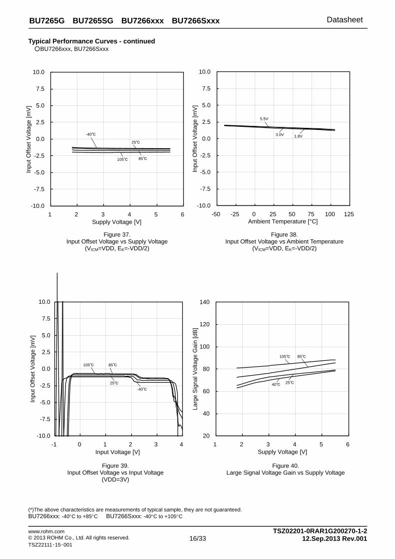
Figure 37. Input Offset Voltage vs Supply Voltage
(VICM=VDD, EK=-VDD/2)
Figure 38. Input Offset Voltage vs Ambient Temperature
(VICM=VDD, EK=-VDD/2)
Figure 39. Input Offset Voltage vs Input Voltage
(VDD=3V)
Figure 40. Large Signal Voltage Gain vs Supply Voltage
-40
25
85 105
5.5V
1.8V 3.0V
-40
25
85 105
40 25
85 105
Datasheet
www.rohm.com TSZ02201-0RAR1G200270-1-2 © 2013 ROHM Co., Ltd. All rights reserved. 17/33 12.Sep.2013 Rev.001 TSZ22111・15・001
BU7265G BU7265SG BU7266xxx BU7266Sxxx
Typical Performance Curves - continued BU7266xxx, BU7266Sxxx
(*)The above characteristics are measurements of typical sample, they are not guaranteed. BU7266xxx: -40C to +85C BU7266Sxxx: -40C to +105C
20
40
60
80
100
120
140
-50 -25 0 25 50 75 100 125Ambient Temperature [°C]
La
rge
Sig
na
l Vo
ltag
e G
ain
[d
B]
0
20
40
60
80
100
120
1 2 3 4 5 6Supply Voltage [V]
Com
mon
Mod
e R
eje
ctio
n R
atio
[d
B]
0
20
40
60
80
100
120
-50 -25 0 25 50 75 100 125Ambient Temperature [°C]
Com
mo
n M
ode
Re
ject
ion
Rat
io [d
B]
0
20
40
60
80
100
120
140
-50 -25 0 25 50 75 100 125Ambient Temperature [°C]
Po
we
r S
up
ply
Re
ject
ion
Ra
tio [
dB
]
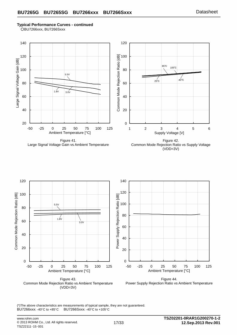
Figure 41. Large Signal Voltage Gain vs Ambient Temperature
Figure 42. Common Mode Rejection Ratio vs Supply Voltage
(VDD=3V)
Figure 43. Common Mode Rejection Ratio vs Ambient Temperature
(VDD=3V)
Figure 44. Power Supply Rejection Ratio vs Ambient Temperature
5.5V
1.8V 3.0V
-40 25
85 105
5.5V
1.8V 3.0V
Datasheet
www.rohm.com TSZ02201-0RAR1G200270-1-2 © 2013 ROHM Co., Ltd. All rights reserved. 18/33 12.Sep.2013 Rev.001 TSZ22111・15・001
BU7265G BU7265SG BU7266xxx BU7266Sxxx
Typical Performance Curves - continued BU7266xxx, BU7266Sxxx
(*)The above characteristics are measurements of typical sample, they are not guaranteed. BU7266xxx: -40C to +85C BU7266Sxxx: -40C to +105C
0
20
40
60
80
100
1.E+00 1.E+01 1.E+02 1.E+03 1.E+04 1.E+05 1.E+06
Frequency [Hz]
Vo
ltag
e G
ain
[dB
]
0
50
100
150
200
Ph
ase
[d
eg
]-4
-2
0
2
4
6
8
-50 -25 0 25 50 75 100 125Ambient Temperature [°C]
Sle
w R
ate
L-H
[V
/ms]
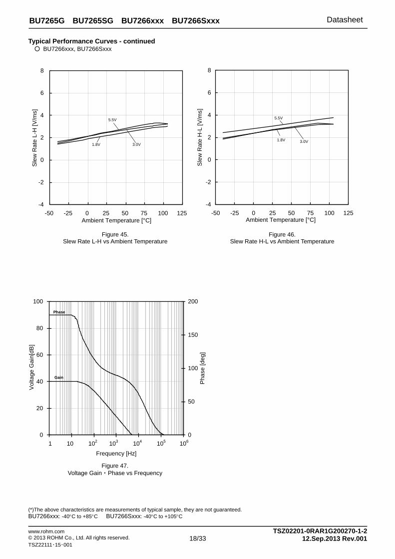
Figure 45. Slew Rate L-H vs Ambient Temperature
-4
-2
0
2
4
6
8
-50 -25 0 25 50 75 100 125Ambient Temperature [°C]
Sle
w R
ate
H-L
[V
/ms]
Figure 46. Slew Rate H-L vs Ambient Temperature
Figure 47. Voltage Gain・Phase vs Frequency
5.5V
1.8V 3.0V
5.5V
1.8V 3.0V
Phase
Gain
1 10 102 103 104 105 106
Datasheet
www.rohm.com TSZ02201-0RAR1G200270-1-2 © 2013 ROHM Co., Ltd. All rights reserved. 19/33 12.Sep.2013 Rev.001 TSZ22111・15・001
BU7265G BU7265SG BU7266xxx BU7266Sxxx
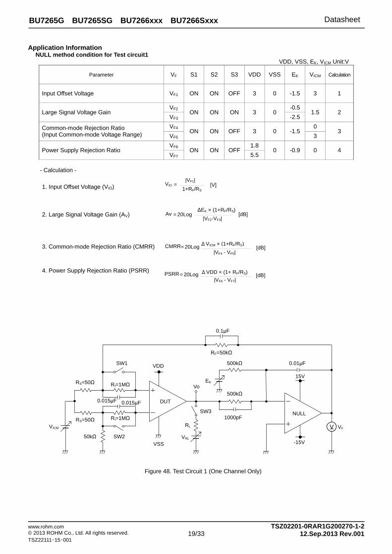
Application Information
NULL method condition for Test circuit1 VDD, VSS, EK, VICM Unit:V
Parameter VF S1 S2 S3 VDD VSS EK VICM Calculation
Input Offset Voltage VF1 ON ON OFF 3 0 -1.5 3 1
Large Signal Voltage Gain VF2
ON ON ON 3 0 -0.5
1.5 2 VF3 -2.5
Common-mode Rejection Ratio (Input Common-mode Voltage Range)
VF4ON ON OFF 3 0 -1.5
0 3
VF5 3
Power Supply Rejection Ratio VF6
ON ON OFF1.8
0 -0.9 0 4 VF7 5.5
- Calculation -
1. Input Offset Voltage (VIO)
2. Large Signal Voltage Gain (AV)
3. Common-mode Rejection Ratio (CMRR)
4. Power Supply Rejection Ratio (PSRR)
VIO
|VF1|=
1+RF/RS
[V]
Av|VF2-VF3|
=ΔEK × (1+RF/RS)
[dB]20Log
CMRR|VF4 - VF5|
=ΔVICM × (1+RF/RS)
[dB]20Log
PSRR|VF6 - VF7|
= ΔVDD × (1+ RF/RS)[dB]20Log
Figure 48. Test Circuit 1 (One Channel Only)
VICM
RS=50Ω
RS=50Ω
RF=50kΩ
RI=1MΩ
RI=1MΩ
0.015μF 0.015μF
SW1
SW2 50kΩ
SW3
RL
VRL
0.1μF
EK
500kΩ
500kΩ
1000pF
VF
0.01μF
15V
-15V
VDD
VSS
Vo
V
NULL
DUT
Datasheet
www.rohm.com TSZ02201-0RAR1G200270-1-2 © 2013 ROHM Co., Ltd. All rights reserved. 20/33 12.Sep.2013 Rev.001 TSZ22111・15・001
BU7265G BU7265SG BU7266xxx BU7266Sxxx
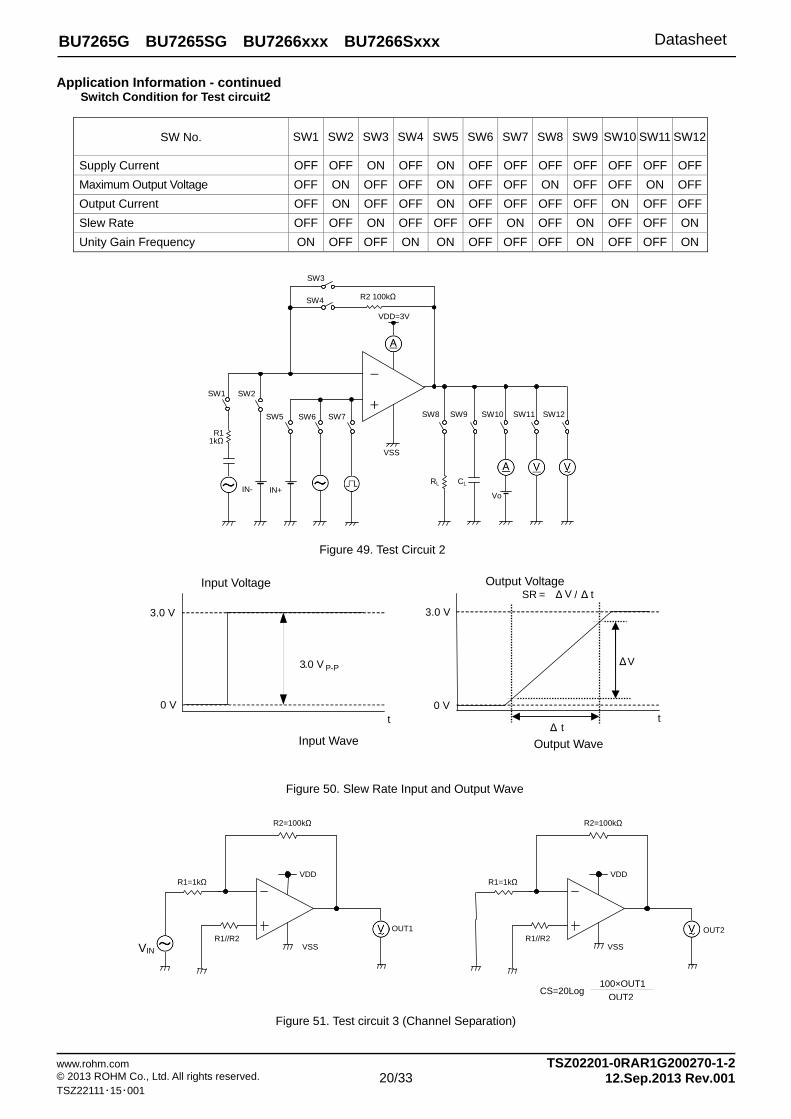
Application Information - continued Switch Condition for Test circuit2
SW No. SW1 SW2 SW3 SW4 SW5 SW6 SW7 SW8 SW9 SW10 SW11 SW12
Supply Current OFF OFF ON OFF ON OFF OFF OFF OFF OFF OFF OFF
Maximum Output Voltage OFF ON OFF OFF ON OFF OFF ON OFF OFF ON OFF
Output Current OFF ON OFF OFF ON OFF OFF OFF OFF ON OFF OFF
Slew Rate OFF OFF ON OFF OFF OFF ON OFF ON OFF OFF ON
Unity Gain Frequency ON OFF OFF ON ON OFF OFF OFF ON OFF OFF ON
Figure 49. Test Circuit 2
Figure 50. Slew Rate Input and Output Wave
Figure 51. Test circuit 3 (Channel Separation)
SW3
SW1 SW2
-
+SW9 SW10 SW11SW8 SW5 SW6 SW7
CL
SW12
SW4
R1 1kΩ
R2 100kΩ
RL
VSS
VDD=3V
VoIN- IN+
t
3.0 V P-P
3.0 V
0 V
SR = ΔV / Δ t
Δ tt
3.0 V
0 V
ΔV
Input Voltage Output Voltage
Input Wave Output Wave
R2=100kΩ
R1=1kΩ VDD
VSS
OUT1
VIN R1//R2
OUT2
R2=100kΩ
R1=1kΩ VDD
VSS R1//R2
CS=20Log 100×OUT1
OUT2
Datasheet
www.rohm.com TSZ02201-0RAR1G200270-1-2 © 2013 ROHM Co., Ltd. All rights reserved. 21/33 12.Sep.2013 Rev.001 TSZ22111・15・001
BU7265G BU7265SG BU7266xxx BU7266Sxxx
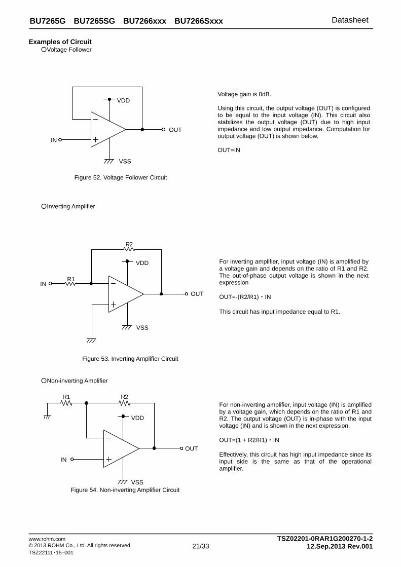
Examples of Circuit Voltage Follower
Inverting Amplifier
Non-inverting Amplifier
Figure 53. Inverting Amplifier Circuit
Figure 54. Non-inverting Amplifier Circuit
Figure 52. Voltage Follower Circuit
Voltage gain is 0dB. Using this circuit, the output voltage (OUT) is configured to be equal to the input voltage (IN). This circuit also stabilizes the output voltage (OUT) due to high input impedance and low output impedance. Computation for output voltage (OUT) is shown below. OUT=IN
For inverting amplifier, input voltage (IN) is amplified by a voltage gain and depends on the ratio of R1 and R2. The out-of-phase output voltage is shown in the next expression OUT=-(R2/R1)・IN This circuit has input impedance equal to R1.
For non-inverting amplifier, input voltage (IN) is amplified by a voltage gain, which depends on the ratio of R1 and R2. The output voltage (OUT) is in-phase with the input voltage (IN) and is shown in the next expression. OUT=(1 + R2/R1)・IN Effectively, this circuit has high input impedance since its input side is the same as that of the operational amplifier.
VSS
OUT
IN
VDD
R 2
R 1
VSS
IN
OUT
VDD
VSS
R2
VDD
IN
OUT
R1
Datasheet
www.rohm.com TSZ02201-0RAR1G200270-1-2 © 2013 ROHM Co., Ltd. All rights reserved. 22/33 12.Sep.2013 Rev.001 TSZ22111・15・001
BU7265G BU7265SG BU7266xxx BU7266Sxxx
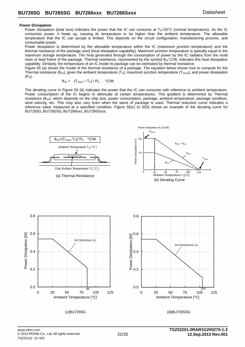
Power Dissipation Power dissipation (total loss) indicates the power that the IC can consume at TA=25°C (normal temperature). As the IC consumes power, it heats up, causing its temperature to be higher than the ambient temperature. The allowable temperature that the IC can accept is limited. This depends on the circuit configuration, manufacturing process, and consumable power. Power dissipation is determined by the allowable temperature within the IC (maximum junction temperature) and the thermal resistance of the package used (heat dissipation capability). Maximum junction temperature is typically equal to the maximum storage temperature. The heat generated through the consumption of power by the IC radiates from the mold resin or lead frame of the package. Thermal resistance, represented by the symbol θJA°C/W, indicates this heat dissipation capability. Similarly, the temperature of an IC inside its package can be estimated by thermal resistance. Figure 55 (a) shows the model of the thermal resistance of a package. The equation below shows how to compute for the Thermal resistance (θJA), given the ambient temperature (TA), maximum junction temperature (TJmax), and power dissipation (PD). θJA = (TJmax-TA) / PD °C/W The derating curve in Figure 55 (b) indicates the power that the IC can consume with reference to ambient temperature. Power consumption of the IC begins to attenuate at certain temperatures. This gradient is determined by Thermal resistance (θJA), which depends on the chip size, power consumption, package, ambient temperature, package condition, wind velocity, etc. This may also vary even when the same of package is used. Thermal reduction curve indicates a reference value measured at a specified condition. Figure 55(c) to 55(f) shows an example of the derating curve for BU7265G, BU7265SG, BU7266xxx, BU7266Sxxx.
(c)BU7265G (d)BU7265SG
0.0
0.2
0.4
0.6
0.8
0 25 50 75 100 125Ambient Temperature [°C]
Po
we
r D
issi
pa
tion
[W
]
0.0
0.2
0.4
0.6
0.8
0 25 50 75 100 125Ambient Temperature [°C]
Po
we
r D
issi
pa
tion
[W
]
BU7265G(Note 14)
BU7265SG(Note 14)
85 105
θJA=(TJmax-TA)/ PD °C/W
Ambient Temperature TA [ °C ]
Chip Surface Temperature TJ [ °C ]
(a) Thermal Resistance 0
Ambient Temperature TA[C]
P1
25 12575 100 50
Power dissipation of LSI [W]
PDmax
TJmax
θJA2
θJA1
θJA2 < θJA1
(b) Derating Curve
P2
Po
we
r D
issi
patio
n o
f IC
Datasheet
www.rohm.com TSZ02201-0RAR1G200270-1-2 © 2013 ROHM Co., Ltd. All rights reserved. 23/33 12.Sep.2013 Rev.001 TSZ22111・15・001
BU7265G BU7265SG BU7266xxx BU7266Sxxx
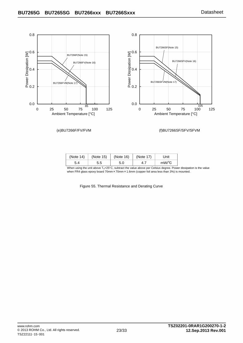
(Note 14) (Note 15) (Note 16) (Note 17) Unit
5.4 5.5 5.0 4.7 mW/ When using the unit above TA=25C, subtract the value above per Celsius degree. Power dissipation is the value when FR4 glass epoxy board 70mm×70mm×1.6mm (copper foil area less than 3%) is mounted.
Figure 55. Thermal Resistance and Derating Curve
(e)BU7266F/FV/FVM (f)BU7266SF/SFV/SFVM
0.0
0.2
0.4
0.6
0.8
0 25 50 75 100 125Ambient Temperature [°C]
Po
we
r D
issi
pat
ion
[W
]
0.0
0.2
0.4
0.6
0.8
0 25 50 75 100 125Ambient Temperature [°C]
Po
we
r D
issi
pa
tion
[W
]
BU7266F(Note 15)
BU7266FV(Note 16)
BU7266FVM(Note 17)
BU7266SF(Note 15)
BU7266SFV(Note 16)
BU7266SFVM(Note 17)
85 105
Datasheet
www.rohm.com TSZ02201-0RAR1G200270-1-2 © 2013 ROHM Co., Ltd. All rights reserved. 24/33 12.Sep.2013 Rev.001 TSZ22111・15・001
BU7265G BU7265SG BU7266xxx BU7266Sxxx
Operational Notes
1. Reverse Connection of Power Supply Connecting the power supply in reverse polarity can damage the IC. Take precautions against reverse polarity when connecting the power supply, such as mounting an external diode between the power supply and the IC’s power supply pins.
2. Power Supply Lines Design the PCB layout pattern to provide low impedance supply lines. Separate the ground and supply lines of the digital and analog blocks to prevent noise in the ground and supply lines of the digital block from affecting the analog block. Furthermore, connect a capacitor to ground at all power supply pins. Consider the effect of temperature and aging on the capacitance value when using electrolytic capacitors.
3. Ground Voltage Ensure that no pins are at a voltage below that of the ground pin at any time, even during transient condition.
4. Ground Wiring Pattern
When using both small-signal and large-current ground traces, the two ground traces should be routed separately but connected to a single ground at the reference point of the application board to avoid fluctuations in the small-signal ground caused by large currents. Also ensure that the ground traces of external components do not cause variations on the ground voltage. The ground lines must be as short and thick as possible to reduce line impedance.
5. Thermal Consideration
Should by any chance the power dissipation rating be exceeded the rise in temperature of the chip may result in deterioration of the properties of the chip. The absolute maximum rating of the PD stated in this specification is when the IC is mounted on a 70mm x 70mm x 1.6mm glass epoxy board. In case of exceeding this absolute maximum rating, increase the board size and copper area to prevent exceeding the PD rating.
6. Recommended Operating Conditions
These conditions represent a range within which the expected characteristics of the IC can be approximately obtained. The electrical characteristics are guaranteed under the conditions of each parameter.
7. Inrush Current
When power is first supplied to the IC, it is possible that the internal logic may be unstable and inrush current may flow instantaneously due to the internal powering sequence and delays, especially if the IC has more than one power supply. Therefore, give special consideration to power coupling capacitance, power wiring, width of ground wiring, and routing of connections.
8. Operation Under Strong Electromagnetic Field
Operating the IC in the presence of a strong electromagnetic field may cause the IC to malfunction.
9. Testing on Application Boards When testing the IC on an application board, connecting a capacitor directly to a low-impedance output pin may subject the IC to stress. Always discharge capacitors completely after each process or step. The IC’s power supply should always be turned off completely before connecting or removing it from the test setup during the inspection process. To prevent damage from static discharge, ground the IC during assembly and use similar precautions during transport and storage.
10. Inter-pin Short and Mounting Errors Ensure that the direction and position are correct when mounting the IC on the PCB. Incorrect mounting may result in damaging the IC. Avoid nearby pins being shorted to each other especially to ground, power supply and output pin. Inter-pin shorts could be due to many reasons such as metal particles, water droplets (in very humid environment) and unintentional solder bridge deposited in between pins during assembly to name a few.
11. Unused Input Pins
Input pins of an IC are often connected to the gate of a MOS transistor. The gate has extremely high impedance and extremely low capacitance. If left unconnected, the electric field from the outside can easily charge it. The small charge acquired in this way is enough to produce a significant effect on the conduction through the transistor and cause unexpected operation of the IC. So unless otherwise specified, unused input pins should be connected to the power supply or ground line.
Datasheet
www.rohm.com TSZ02201-0RAR1G200270-1-2 © 2013 ROHM Co., Ltd. All rights reserved. 25/33 12.Sep.2013 Rev.001 TSZ22111・15・001
BU7265G BU7265SG BU7266xxx BU7266Sxxx
Operational Notes – continued
12. Regarding the Input Pin of the IC In the construction of this IC, P-N junctions are inevitably formed creating parasitic diodes or transistors. The operation of these parasitic elements can result in mutual interference among circuits, operational faults, or physical damage. Therefore, conditions which cause these parasitic elements to operate, such as applying a voltage to an input pin lower than the ground voltage should be avoided. Furthermore, do not apply a voltage to the input pins when no power supply voltage is applied to the IC. Even if the power supply voltage is applied, make sure that the input pins have voltages within the values specified in the electrical characteristics of this IC.
13. Unused circuits When there are unused op-amps, it is recommended that they are connected as in Figure 58, setting the non-inverting input terminal to a potential within the in-phase input voltage range (VICM).
14. Input Voltage
Applying VDD+0.3V to the input terminal is possible without causing deterioration of the electrical characteristics or destruction, regardless of the supply voltage. However, this does not ensure normal circuit operation. Please note that the circuit operates normally only when the input voltage is within the common mode input voltage range of the electric characteristics.
15. Power supply(single/dual)
The operational amplifier operates when the voltage supplied is between VDD and VSS. Therefore, the single supply operational amplifiers can be used as dual supply operational amplifiers as well.
16. Output capacitor
If a large capacitor is connected between the output pin and VSS pin, current from the charged capacitor will flow into the output pin and may destroy the IC when the VDD pin is shorted to ground or pulled down to 0V. Use a capacitor smaller than 0.1uF between output pin and VSS pin.
17. Oscillation by output capacitor
Please pay attention to the oscillation by output capacitor and in designing an application of negative feedback loop circuit with these ICs.
18. Latch Up
Be careful of input voltage that exceed the VDD and VSS. When CMOS device have sometimes occur latch up and protect the IC from abnormaly noise.
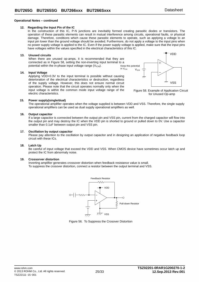
19. Crossorver distortion
Inverting amplifier generates crossover distortion when feedback resistance value is small. To suppress the crosover distortion, connect a resistor between the output terminal and VSS.
Figure 58. Example of Application Circuitfor Unused Op-amp
VDD
VSS
Feedback Resistor
Figure 56. To Suppress the Crosover Distortion
Keep this potential in VICM
VSS
VDD
VICM
Pull-down Resistor
Datasheet
www.rohm.com TSZ02201-0RAR1G200270-1-2 © 2013 ROHM Co., Ltd. All rights reserved. 26/33 12.Sep.2013 Rev.001 TSZ22111・15・001
BU7265G BU7265SG BU7266xxx BU7266Sxxx
Marking Diagram
Product Name Package Type Marking
BU7265 G SSOP5
D3
BU7265S FA
BU7266
F SOP8 7266
FV SSOP-B8 266
FVM MSOP8 7266
BU7266S
F SOP8 7266S
FV SSOP-B8 266S
FVM MSOP8 7266S
SOP8(TOP VIEW)
Part Number Marking
LOT Number
1PIN MARK
SSOP-B8(TOP VIEW)
Part Number Marking
LOT Number
1PIN MARK
MSOP8(TOP VIEW)
Part Number Marking
LOT Number
1PIN MARK
Part Number Marking
SSOP5(TOP VIEW)
LOT Number
Datasheet
www.rohm.com TSZ02201-0RAR1G200270-1-2 © 2013 ROHM Co., Ltd. All rights reserved. 27/33 12.Sep.2013 Rev.001 TSZ22111・15・001
BU7265G BU7265SG BU7266xxx BU7266Sxxx
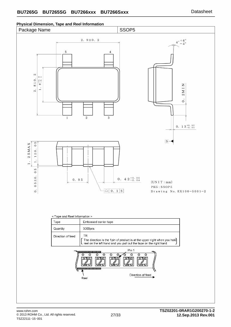
Physical Dimension, Tape and Reel Information
Package Name SSOP5
Datasheet
www.rohm.com TSZ02201-0RAR1G200270-1-2 © 2013 ROHM Co., Ltd. All rights reserved. 28/33 12.Sep.2013 Rev.001 TSZ22111・15・001
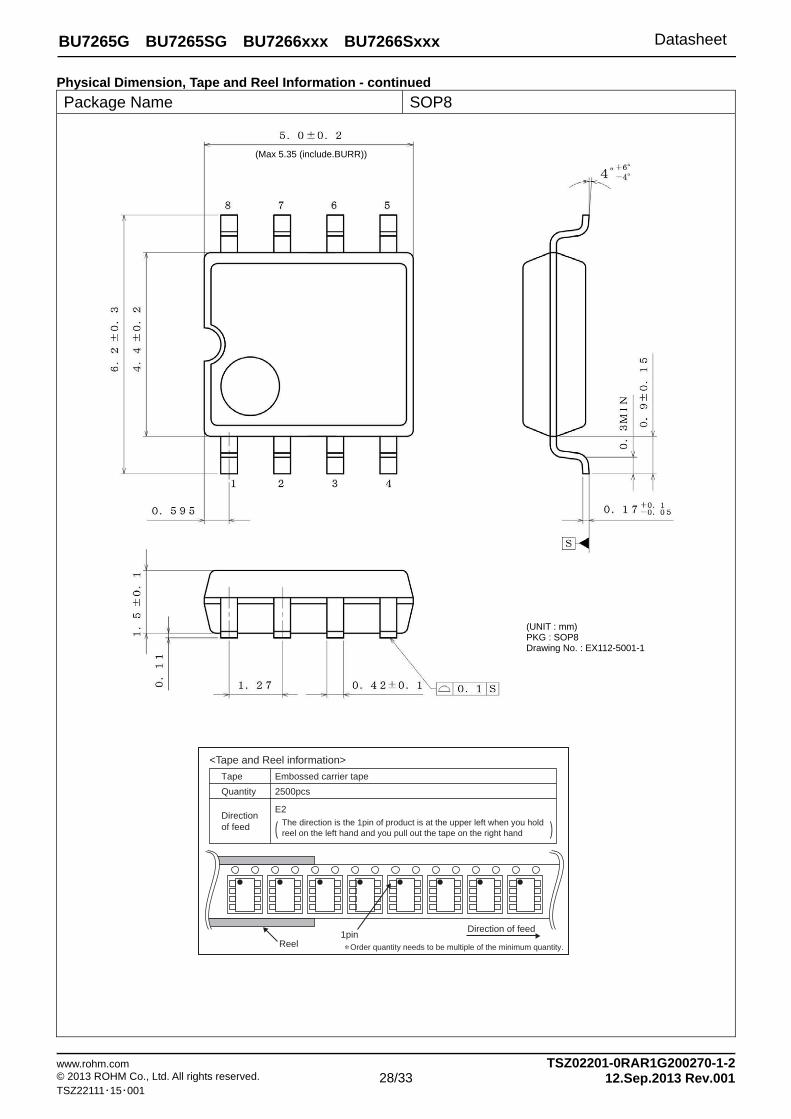
BU7265G BU7265SG BU7266xxx BU7266Sxxx
Physical Dimension, Tape and Reel Information - continued
Package Name SOP8
∗ Order quantity needs to be multiple of the minimum quantity.
<Tape and Reel information>
Embossed carrier tapeTape
Quantity
Direction of feed The direction is the 1pin of product is at the upper left when you hold
reel on the left hand and you pull out the tape on the right hand
2500pcs
E2
( )
Direction of feed
Reel1pin
(UNIT : mm) PKG : SOP8 Drawing No. : EX112-5001-1
(Max 5.35 (include.BURR))
Datasheet
www.rohm.com TSZ02201-0RAR1G200270-1-2 © 2013 ROHM Co., Ltd. All rights reserved. 29/33 12.Sep.2013 Rev.001 TSZ22111・15・001
BU7265G BU7265SG BU7266xxx BU7266Sxxx
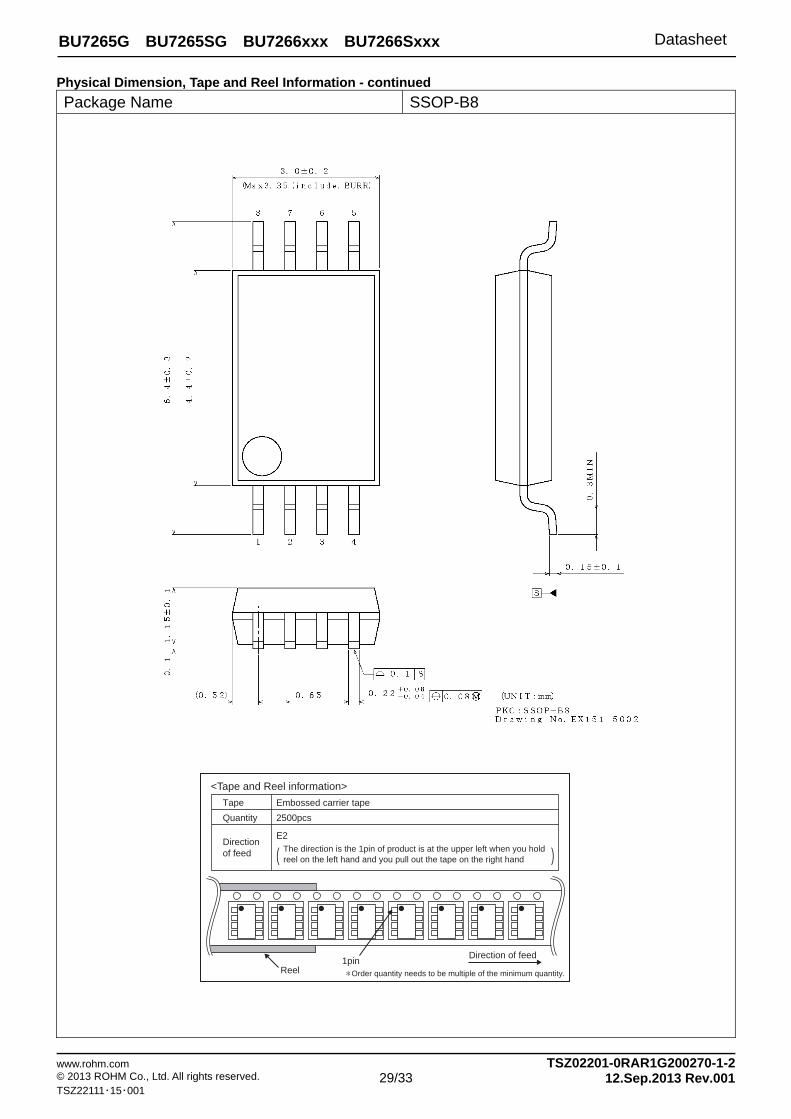
Physical Dimension, Tape and Reel Information - continued
Package Name SSOP-B8
∗ Order quantity needs to be multiple of the minimum quantity.
<Tape and Reel information>
Embossed carrier tapeTape
Quantity
Direction of feed The direction is the 1pin of product is at the upper left when you hold
reel on the left hand and you pull out the tape on the right hand
2500pcs
E2
( )
Direction of feed
Reel1pin
Datasheet
www.rohm.com TSZ02201-0RAR1G200270-1-2 © 2013 ROHM Co., Ltd. All rights reserved. 30/33 12.Sep.2013 Rev.001 TSZ22111・15・001
BU7265G BU7265SG BU7266xxx BU7266Sxxx
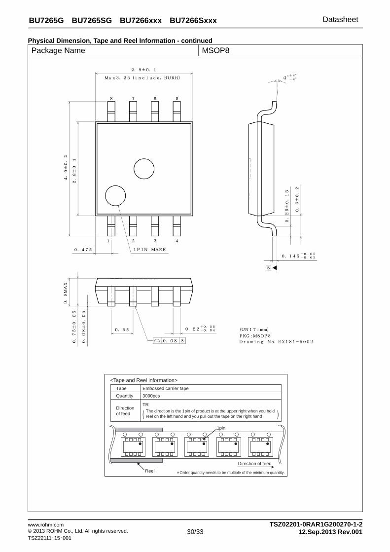
Physical Dimension, Tape and Reel Information - continued
Package Name MSOP8
Direction of feed
Reel ∗ Order quantity needs to be multiple of the minimum quantity.
<Tape and Reel information>
Embossed carrier tapeTape
Quantity
Direction of feed
The direction is the 1pin of product is at the upper right when you hold reel on the left hand and you pull out the tape on the right hand
3000pcs
TR
( )1pin
Datasheet
www.rohm.com TSZ02201-0RAR1G200270-1-2 © 2013 ROHM Co., Ltd. All rights reserved. 31/33 12.Sep.2013 Rev.001 TSZ22111・15・001
BU7265G BU7265SG BU7266xxx BU7266Sxxx
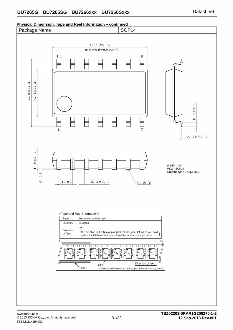
Physical Dimension, Tape and Reel Information – continued
Package Name SOP14
∗ Order quantity needs to be multiple of the minimum quantity.
<Tape and Reel information>
Embossed carrier tapeTape
Quantity
Direction of feed
The direction is the 1pin of product is at the upper left when you hold reel on the left hand and you pull out the tape on the right hand
2500pcs
E2
( )
Direction of feed
Reel1pin
(UNIT : mm) PKG : SOP14 Drawing No. : EX113-5001
(Max 9.05 (include.BURR))
Datasheet
www.rohm.com TSZ02201-0RAR1G200270-1-2 © 2013 ROHM Co., Ltd. All rights reserved. 32/33 12.Sep.2013 Rev.001 TSZ22111・15・001
BU7265G BU7265SG BU7266xxx BU7266Sxxx
Physical Dimension, Tape and Reel Information – continued
Package Name SSOP-B14
∗ Order quantity needs to be multiple of the minimum quantity.
<Tape and Reel information>
Embossed carrier tapeTape
Quantity
Direction of feed
The direction is the 1pin of product is at the upper left when you hold reel on the left hand and you pull out the tape on the right hand
2500pcs
E2
( )
Direction of feed
Reel1pin
Datasheet
www.rohm.com TSZ02201-0RAR1G200270-1-2 © 2013 ROHM Co., Ltd. All rights reserved. 33/33 12.Sep.2013 Rev.001 TSZ22111・15・001
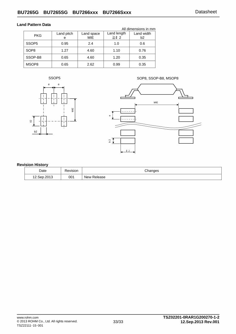
BU7265G BU7265SG BU7266xxx BU7266Sxxx
e
MIE
ℓ2
b2
e
Land Pattern Data All dimensions in mm
PKG Land pitch
e Land space
MIE Land length
≧ℓ 2 Land width
b2
SSOP5 0.95 2.4 1.0 0.6
SOP8 1.27 4.60 1.10 0.76
SSOP-B8 0.65 4.60 1.20 0.35
MSOP8 0.65 2.62 0.99 0.35
Revision History
Date Revision Changes
12.Sep.2013 001 New Release
SSOP5 SOP8, SSOP-B8, MSOP8
MIE
ℓ 2
b 2
e
DatasheetDatasheet
Notice - GE Rev.002© 2014 ROHM Co., Ltd. All rights reserved.
Notice Precaution on using ROHM Products
1. Our Products are designed and manufactured for application in ordinary electronic equipments (such as AV equipment, OA equipment, telecommunication equipment, home electronic appliances, amusement equipment, etc.). If you intend to use our Products in devices requiring extremely high reliability (such as medical equipment (Note 1), transport equipment, traffic equipment, aircraft/spacecraft, nuclear power controllers, fuel controllers, car equipment including car accessories, safety devices, etc.) and whose malfunction or failure may cause loss of human life, bodily injury or serious damage to property (“Specific Applications”), please consult with the ROHM sales representative in advance. Unless otherwise agreed in writing by ROHM in advance, ROHM shall not be in any way responsible or liable for any damages, expenses or losses incurred by you or third parties arising from the use of any ROHM’s Products for Specific Applications.
(Note1) Medical Equipment Classification of the Specific Applications JAPAN USA EU CHINA
CLASSⅢ CLASSⅢ
CLASSⅡb CLASSⅢ
CLASSⅣ CLASSⅢ
2. ROHM designs and manufactures its Products subject to strict quality control system. However, semiconductor
products can fail or malfunction at a certain rate. Please be sure to implement, at your own responsibilities, adequate safety measures including but not limited to fail-safe design against the physical injury, damage to any property, which a failure or malfunction of our Products may cause. The following are examples of safety measures:
[a] Installation of protection circuits or other protective devices to improve system safety [b] Installation of redundant circuits to reduce the impact of single or multiple circuit failure
3. Our Products are designed and manufactured for use under standard conditions and not under any special or extraordinary environments or conditions, as exemplified below. Accordingly, ROHM shall not be in any way responsible or liable for any damages, expenses or losses arising from the use of any ROHM’s Products under any special or extraordinary environments or conditions. If you intend to use our Products under any special or extraordinary environments or conditions (as exemplified below), your independent verification and confirmation of product performance, reliability, etc, prior to use, must be necessary:
[a] Use of our Products in any types of liquid, including water, oils, chemicals, and organic solvents [b] Use of our Products outdoors or in places where the Products are exposed to direct sunlight or dust [c] Use of our Products in places where the Products are exposed to sea wind or corrosive gases, including Cl2,
H2S, NH3, SO2, and NO2
[d] Use of our Products in places where the Products are exposed to static electricity or electromagnetic waves [e] Use of our Products in proximity to heat-producing components, plastic cords, or other flammable items [f] Sealing or coating our Products with resin or other coating materials [g] Use of our Products without cleaning residue of flux (even if you use no-clean type fluxes, cleaning residue of
flux is recommended); or Washing our Products by using water or water-soluble cleaning agents for cleaning residue after soldering
[h] Use of the Products in places subject to dew condensation
4. The Products are not subject to radiation-proof design. 5. Please verify and confirm characteristics of the final or mounted products in using the Products. 6. In particular, if a transient load (a large amount of load applied in a short period of time, such as pulse. is applied,
confirmation of performance characteristics after on-board mounting is strongly recommended. Avoid applying power exceeding normal rated power; exceeding the power rating under steady-state loading condition may negatively affect product performance and reliability.
7. De-rate Power Dissipation (Pd) depending on Ambient temperature (Ta). When used in sealed area, confirm the actual
ambient temperature. 8. Confirm that operation temperature is within the specified range described in the product specification. 9. ROHM shall not be in any way responsible or liable for failure induced under deviant condition from what is defined in
this document.
Precaution for Mounting / Circuit board design 1. When a highly active halogenous (chlorine, bromine, etc.) flux is used, the residue of flux may negatively affect product
performance and reliability. 2. In principle, the reflow soldering method must be used; if flow soldering method is preferred, please consult with the
ROHM representative in advance. For details, please refer to ROHM Mounting specification
DatasheetDatasheet
Notice - GE Rev.002© 2014 ROHM Co., Ltd. All rights reserved.
Precautions Regarding Application Examples and External Circuits 1. If change is made to the constant of an external circuit, please allow a sufficient margin considering variations of the
characteristics of the Products and external components, including transient characteristics, as well as static characteristics.
2. You agree that application notes, reference designs, and associated data and information contained in this document
are presented only as guidance for Products use. Therefore, in case you use such information, you are solely responsible for it and you must exercise your own independent verification and judgment in the use of such information contained in this document. ROHM shall not be in any way responsible or liable for any damages, expenses or losses incurred by you or third parties arising from the use of such information.
Precaution for Electrostatic
This Product is electrostatic sensitive product, which may be damaged due to electrostatic discharge. Please take proper caution in your manufacturing process and storage so that voltage exceeding the Products maximum rating will not be applied to Products. Please take special care under dry condition (e.g. Grounding of human body / equipment / solder iron, isolation from charged objects, setting of Ionizer, friction prevention and temperature / humidity control).
Precaution for Storage / Transportation 1. Product performance and soldered connections may deteriorate if the Products are stored in the places where:
[a] the Products are exposed to sea winds or corrosive gases, including Cl2, H2S, NH3, SO2, and NO2 [b] the temperature or humidity exceeds those recommended by ROHM [c] the Products are exposed to direct sunshine or condensation [d] the Products are exposed to high Electrostatic
2. Even under ROHM recommended storage condition, solderability of products out of recommended storage time period may be degraded. It is strongly recommended to confirm solderability before using Products of which storage time is exceeding the recommended storage time period.
3. Store / transport cartons in the correct direction, which is indicated on a carton with a symbol. Otherwise bent leads
may occur due to excessive stress applied when dropping of a carton. 4. Use Products within the specified time after opening a humidity barrier bag. Baking is required before using Products of
which storage time is exceeding the recommended storage time period.
Precaution for Product Label QR code printed on ROHM Products label is for ROHM’s internal use only.
Precaution for Disposition When disposing Products please dispose them properly using an authorized industry waste company.
Precaution for Foreign Exchange and Foreign Trade act Since our Products might fall under controlled goods prescribed by the applicable foreign exchange and foreign trade act, please consult with ROHM representative in case of export.
Precaution Regarding Intellectual Property Rights 1. All information and data including but not limited to application example contained in this document is for reference
only. ROHM does not warrant that foregoing information or data will not infringe any intellectual property rights or any other rights of any third party regarding such information or data. ROHM shall not be in any way responsible or liable for infringement of any intellectual property rights or other damages arising from use of such information or data.:
2. No license, expressly or implied, is granted hereby under any intellectual property rights or other rights of ROHM or any
third parties with respect to the information contained in this document.
Other Precaution 1. This document may not be reprinted or reproduced, in whole or in part, without prior written consent of ROHM. 2. The Products may not be disassembled, converted, modified, reproduced or otherwise changed without prior written
consent of ROHM. 3. In no event shall you use in any way whatsoever the Products and the related technical information contained in the
Products or this document for any military purposes, including but not limited to, the development of mass-destruction weapons.
4. The proper names of companies or products described in this document are trademarks or registered trademarks of
ROHM, its affiliated companies or third parties.
DatasheetDatasheet
Notice – WE Rev.001© 2014 ROHM Co., Ltd. All rights reserved.
General Precaution 1. Before you use our Pro ducts, you are requested to care fully read this document and fully understand its contents.
ROHM shall n ot be in an y way responsible or liabl e for fa ilure, malfunction or acci dent arising from the use of a ny ROHM’s Products against warning, caution or note contained in this document.
2. All information contained in this docume nt is current as of the issuing date and subj ect to change without any prior
notice. Before purchasing or using ROHM’s Products, please confirm the la test information with a ROHM sale s representative.
3. The information contained in this doc ument is provi ded on an “as is” basis and ROHM does not warrant that all
information contained in this document is accurate an d/or error-free. ROHM shall not be in an y way responsible or liable for any damages, expenses or losses incurred by you or third parties resulting from inaccuracy or errors of or concerning such information.