Embed Size (px)
Citation preview

Ultra Low Power CMOS Design
Ph.D. Dissertation Proposal
Kyungseok Kim
ECE Auburn Univ.
Chair: Prof. Vishwani D. Agrawal
Committee Members: Prof. Victor P. NelsonProf. Fa F. Dai
May 11, 2010
2
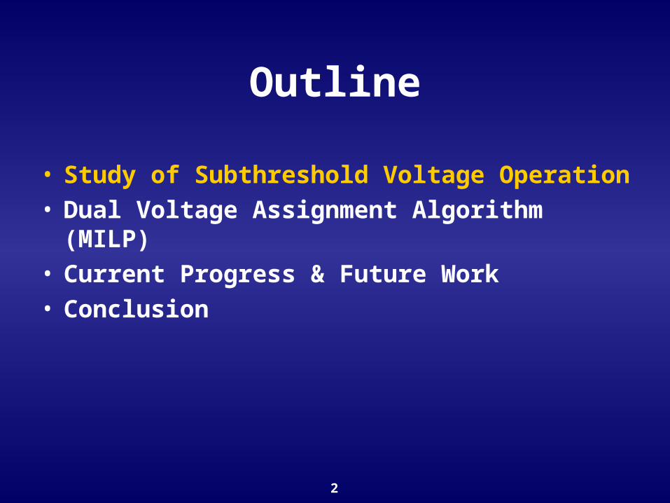
Outline
• Study of Subthreshold Voltage Operation • Dual Voltage Assignment Algorithm (MILP) • Current Progress & Future Work• Conclusion
3
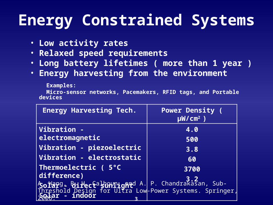
Energy Constrained Systems • Low activity rates • Relaxed speed requirements• Long battery lifetimes ( more than 1 year )• Energy harvesting from the environment
Examples: Micro-sensor networks, Pacemakers, RFID tags, and Portable devices
Energy Harvesting Tech. Power Density ( µW/cm2 )
Vibration - electromagnetic
Vibration - piezoelectric
Vibration - electrostatic
Thermoelectric ( 5°C difference)
Solar - direct sunlight
Solar - indoor
4.0
500
3.8
60
3700
3.2
A. Wang, B. H. Calhoun, and A. P. Chandrakasan, Sub-Threshold Design for Ultra Low-Power Systems. Springer, 2006.
4
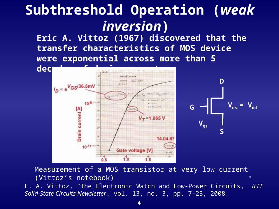
Subthreshold Operation (weak inversion) Eric A. Vittoz (1967) discovered that the transfer characteristics of MOS device were exponential across more than 5 decades of drain current.
Measurement of a MOS transistor at very low current (Vittoz’s notebook)
E. A. Vittoz, “The Electronic Watch and Low-Power Circuits,” IEEE Solid-State Circuits Newsletter, vol. 13, no. 3, pp. 7–23, 2008.
S
D
G
Vgs
Vds = Vdd
5
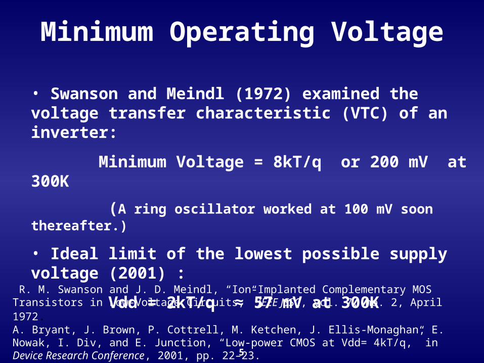
Minimum Operating Voltage
• Swanson and Meindl (1972) examined the voltage transfer characteristic (VTC) of an inverter:
Minimum Voltage = 8kT/q or 200 mV at 300K
(A ring oscillator worked at 100 mV soon thereafter.)
• Ideal limit of the lowest possible supply voltage (2001) :
Vdd = 2kT/q ≈ 57 mV at 300K
R. M. Swanson and J. D. Meindl, “Ion-Implanted Complementary MOS Transistors in Low-Voltage Circuits,” IEEE JSSC, vol. 7, no. 2, April 1972.A. Bryant, J. Brown, P. Cottrell, M. Ketchen, J. Ellis-Monaghan, E. Nowak, I. Div, and E. Junction, “Low-power CMOS at Vdd= 4kT/q,” in Device Research Conference, 2001, pp. 22–23.
6
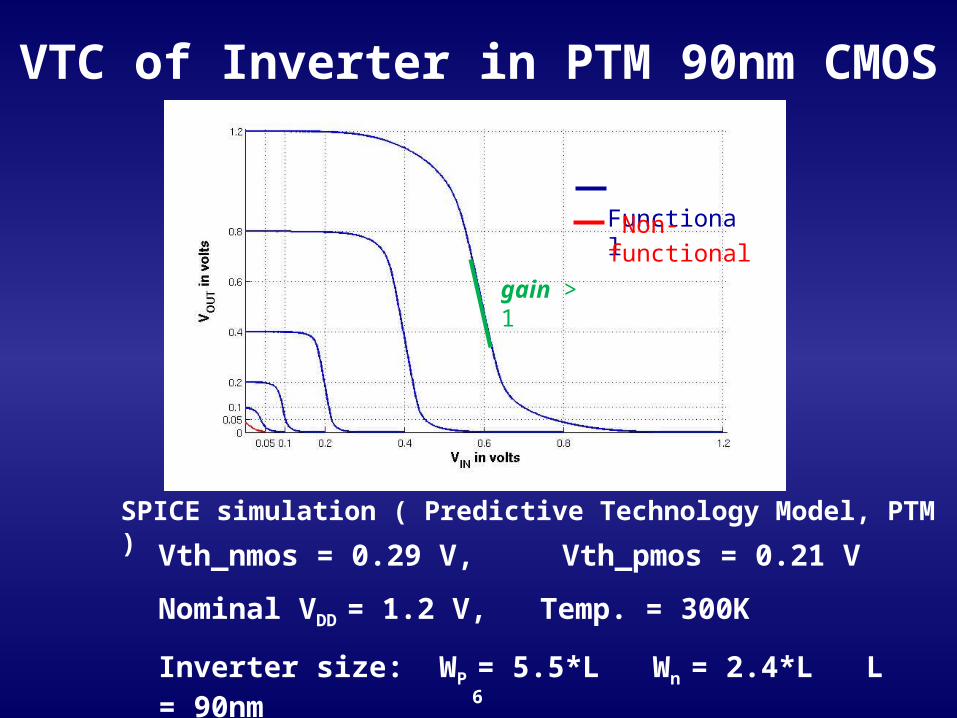
VTC of Inverter in PTM 90nm CMOS
Vth_nmos = 0.29 V, Vth_pmos = 0.21 V
Nominal VDD = 1.2 V, Temp. = 300K
Inverter size: WP = 5.5*L Wn = 2.4*L L = 90nm
SPICE simulation ( Predictive Technology Model, PTM )
gain > 1
Functional
Non-functional
7
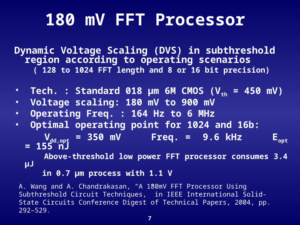
Dynamic Voltage Scaling (DVS) in subthreshold region according to operating scenarios
( 128 to 1024 FFT length and 8 or 16 bit precision)
• Tech. : Standard 018 µm 6M CMOS (Vth = 450 mV)• Voltage scaling: 180 mV to 900 mV• Operating Freq. : 164 Hz to 6 MHz• Optimal operating point for 1024 and 16b: Vdd,opt = 350 mV Freq. = 9.6 kHz Eopt = 155 nJ Above-threshold low power FFT processor consumes 3.4 µJ in 0.7 µm process with 1.1 V
180 mV FFT Processor
A. Wang and A. Chandrakasan, “A 180mV FFT Processor Using Subthreshold Circuit Techniques,” in IEEE International Solid-State Circuits Conference Digest of Technical Papers, 2004, pp. 292–529.
8
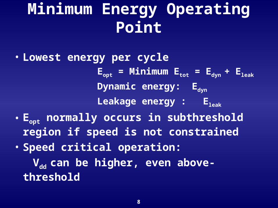
Minimum Energy Operating Point
• Lowest energy per cycle Eopt = Minimum Etot = Edyn + Eleak
Dynamic energy: Edyn
Leakage energy : Eleak
• Eopt normally occurs in subthreshold region if speed is not constrained
• Speed critical operation:
Vdd can be higher, even above-threshold
9
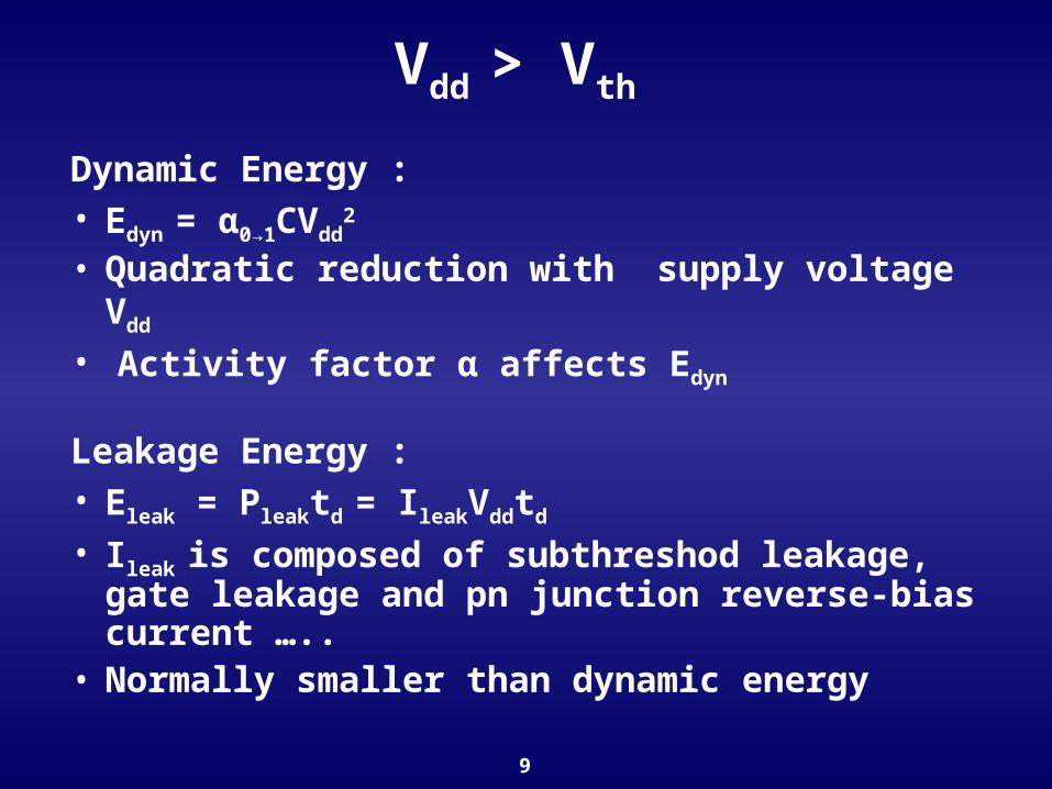
Dynamic Energy : • Edyn = α0→1CVdd
2
• Quadratic reduction with supply voltage Vdd
• Activity factor α affects Edyn
Leakage Energy :• Eleak = Pleaktd = IleakVddtd
• Ileak is composed of subthreshod leakage, gate leakage and pn junction reverse-bias current …..
• Normally smaller than dynamic energy
Vdd > Vth
10
A. Wang, B. H. Calhoun, and A. P. Chandrakasan, Sub-Threshold Design for Ultra Low-Power Systems. Springer, 2006.
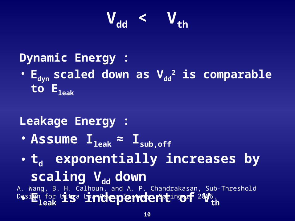
Vdd < Vth
Dynamic Energy : • Edyn scaled down as Vdd
2 is comparable to Eleak
Leakage Energy :
• Assume Ileak ≈ Isub,off
• td exponentially increases by scaling Vdd
down
• Eleak is independent of Vth
11
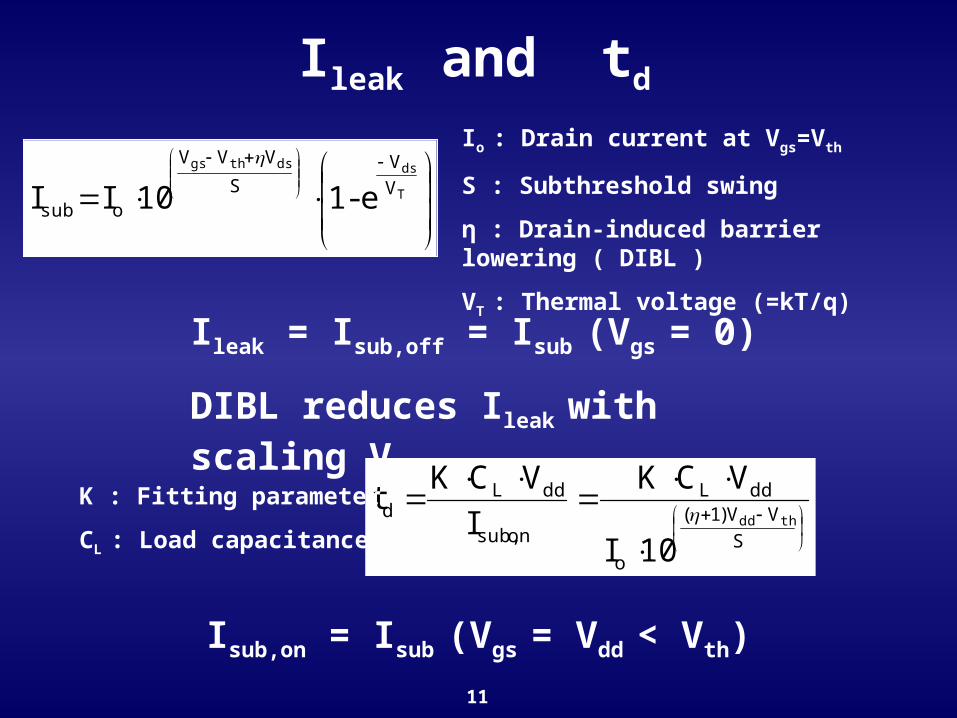
Ileak and td
T
dsdsthgs
V
VS
VVV
osub e-1 10I I
Io : Drain current at Vgs=Vth
S : Subthreshold swing
η : Drain-induced barrier lowering ( DIBL )
VT : Thermal voltage (=kT/q)
Ileak = Isub,off = Isub (Vgs = 0)
DIBL reduces Ileak with scaling Vdd
S
VV)1(
o
ddL
onsub,
ddLd
thdd
10I
VCK
I
VCK t
K : Fitting parameter
CL : Load capacitance
Isub,on = Isub (Vgs = Vdd < Vth)
12
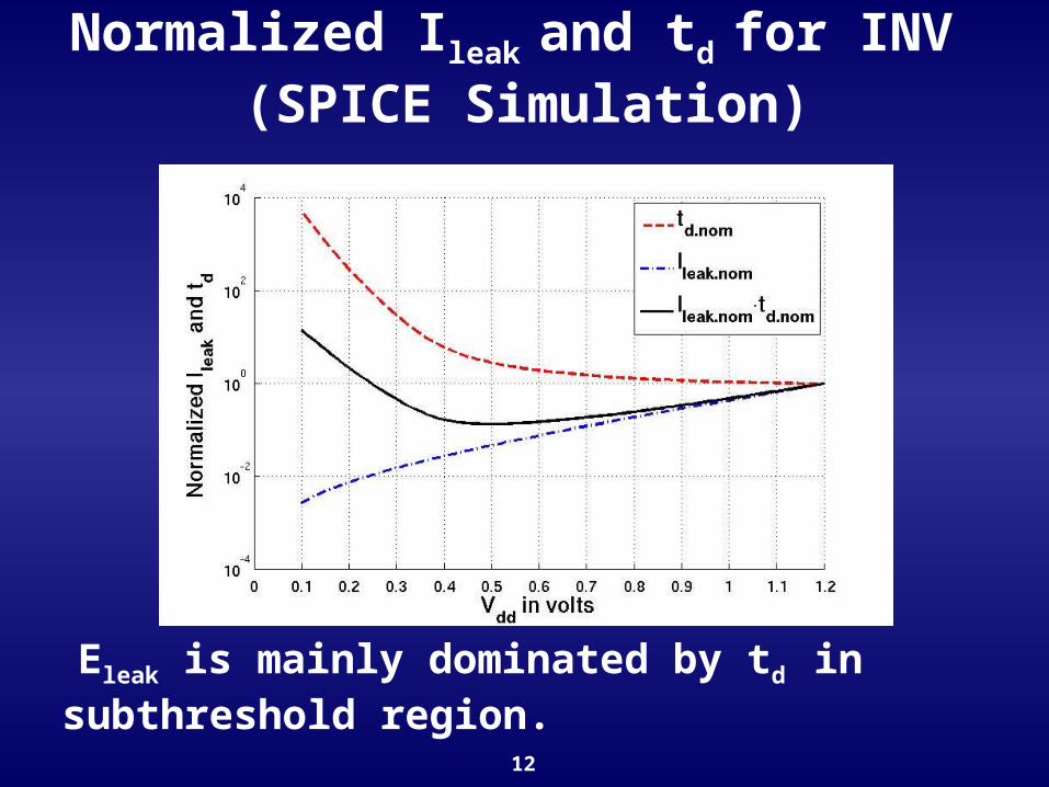
Normalized Ileak and td for INV (SPICE Simulation)
Eleak is mainly dominated by td in subthreshold region.
13
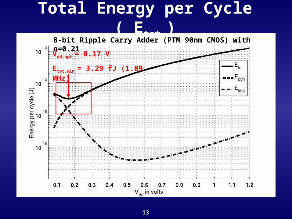
Total Energy per Cycle ( Etot )8-bit Ripple Carry Adder (PTM 90nm CMOS) with α=0.21
Vdd,opt = 0.17 V
Etot,min = 3.29 fJ (1.89 MHz)
14
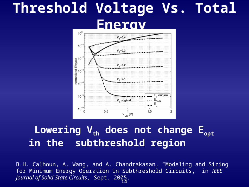
Threshold Voltage Vs. Total Energy
Lowering Vth does not change Eopt in the subthreshold region
B.H. Calhoun, A. Wang, and A. Chandrakasan, “Modeling and Sizing for Minimum Energy Operation in Subthreshold Circuits,” in IEEE Journal of Solid-State Circuits, Sept. 2005.
15
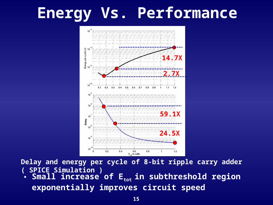
Energy Vs. Performance
• Small increase of Etot in subthreshold region exponentially improves circuit speed
59.1X
14.7X
24.5X
2.7X
Delay and energy per cycle of 8-bit ripple carry adder ( SPICE Simulation )
16
Outline
• Study of Subthreshold Voltage Operation • Dual Voltage Assignment Algorithm (MILP) • Current Progress & Future Work• Conclusion
17
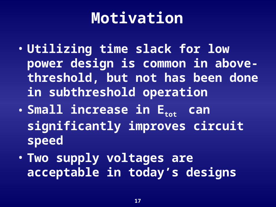
Motivation
• Utilizing time slack for low power design is common in above-threshold, but not has been done in subthreshold operation
• Small increase in Etot can significantly improves circuit speed
• Two supply voltages are acceptable in today’s designs
18
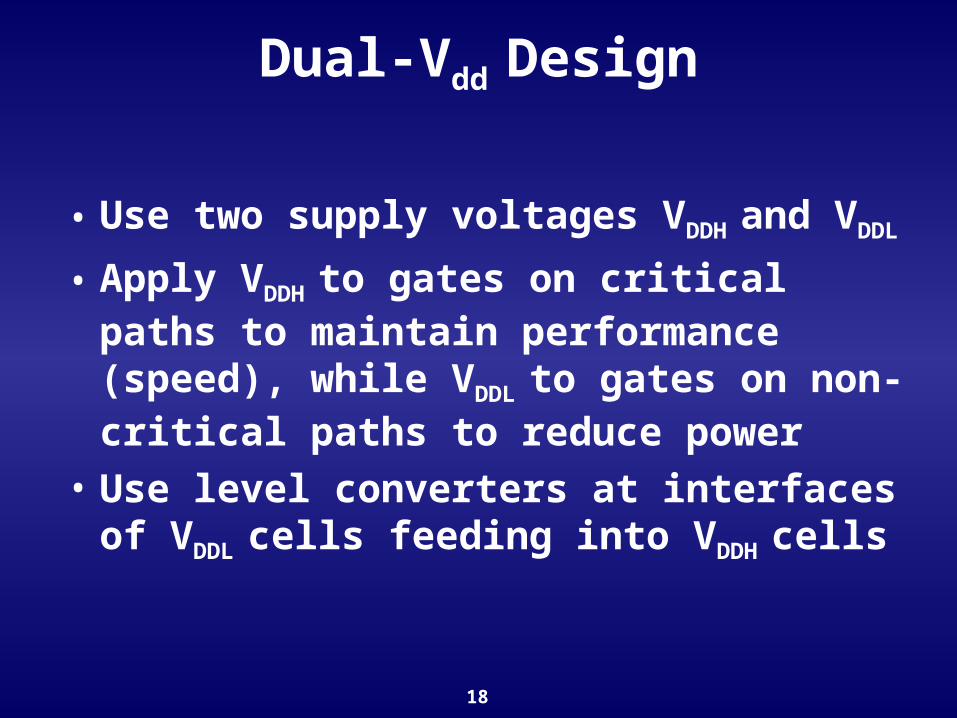
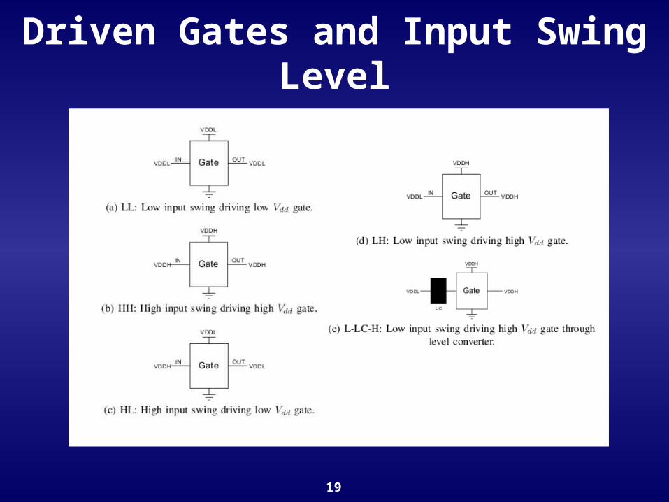
Dual-Vdd Design
• Use two supply voltages VDDH and VDDL
• Apply VDDH to gates on critical paths to maintain performance (speed), while VDDL to gates on non-critical paths to reduce power
• Use level converters at interfaces of VDDL cells feeding into VDDH cells
19
Driven Gates and Input Swing Level
20
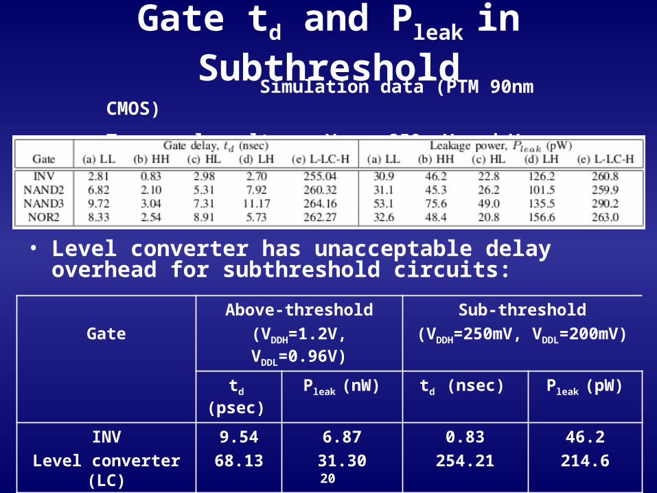
Gate td and Pleak in Subthreshold
• Level converter has unacceptable delay overhead for subthreshold circuits:
Simulation data (PTM 90nm CMOS)
Two supply voltages VDDH = 250 mV and VDDL = 200 mV
Gate
Above-threshold
(VDDH=1.2V, VDDL=0.96V)
Sub-threshold
(VDDH=250mV, VDDL=200mV)
td (psec) Pleak (nW) td (nsec) Pleak (pW)
INV
Level converter (LC)
9.54
68.13
6.87
31.30
0.83
254.21
46.2
214.6
LC norm. to INV 7.1 4.6 306.3 4.7
21
Algorithm I : Eopt for Single Vdd
• Characterize Standard cells for maximum delay, average leakage, and capacitances power using SPICE simulation over subthreshold region (100 mV to 300 mV, 10 mV step, 21 points, PTM 90 nm CMOS)
• Low to high signal activity from logic simulator
• Critical delay Tc from STA (21 points)
• Calculate Etot by the sum of energy for gates
(21 points)
• Find lowest Etot as Eopt
Ci,Vleak,2
idd,iL,iitot, TPVCEdd
22
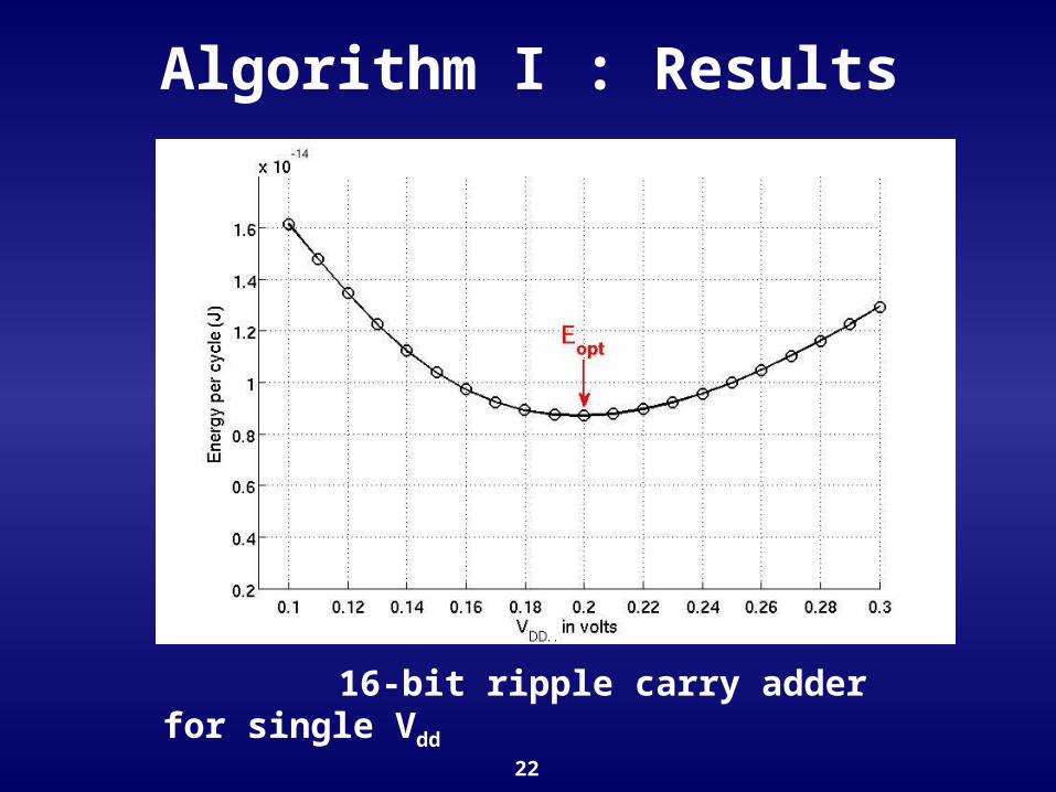
Algorithm I : Results
16-bit ripple carry adder for single Vdd
23
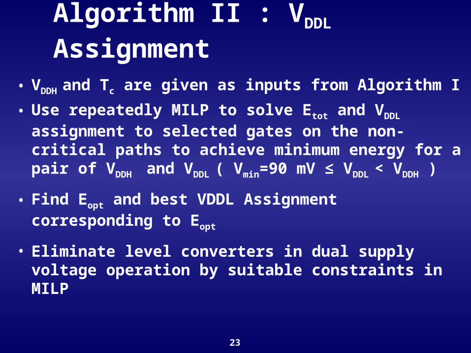
Algorithm II : VDDL Assignment
• VDDH and Tc are given as inputs from Algorithm I
• Use repeatedly MILP to solve Etot and VDDL
assignment to selected gates on the non-critical paths to achieve minimum energy for a pair of VDDH and VDDL ( Vmin=90 mV ≤ VDDL < VDDH )
• Find Eopt and best VDDL Assignment corresponding to Eopt
• Eliminate level converters in dual supply voltage operation by suitable constraints in MILP
24
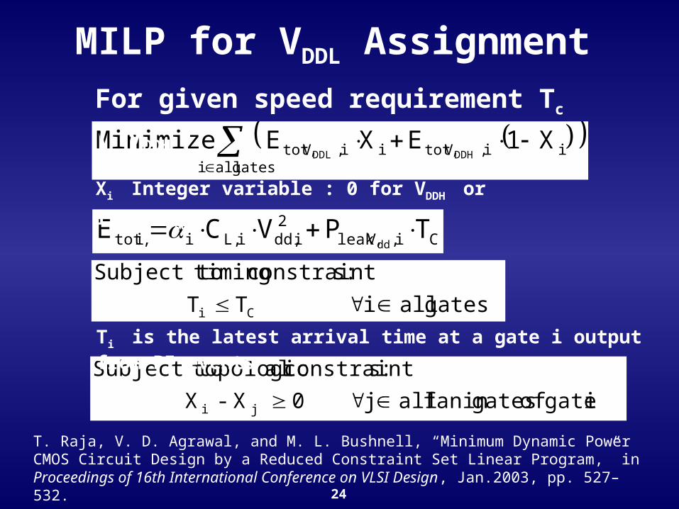
MILP for VDDL Assignment
Ci,Vleak,2
idd,iL,iitot, TPVCEdd
gates all i T T
:sconstraint timingSubject to
Ci
i gate of gatesfanin all j 0 X - X
:sconstraint al topologicSubject to
ji
gates all i
ii,Vtot,ii,Vtot, X1EXE MinimizeDDHDDL
For given speed requirement Tc ( VDDH )
Ti is the latest arrival time at a gate i output from PI events
Xi Integer variable : 0 for VDDH or 1 for VDDL
T. Raja, V. D. Agrawal, and M. L. Bushnell, “Minimum Dynamic Power CMOS Circuit Design by a Reduced Constraint Set Linear Program,” in Proceedings of 16th International Conference on VLSI Design, Jan.2003, pp. 527–532.
25
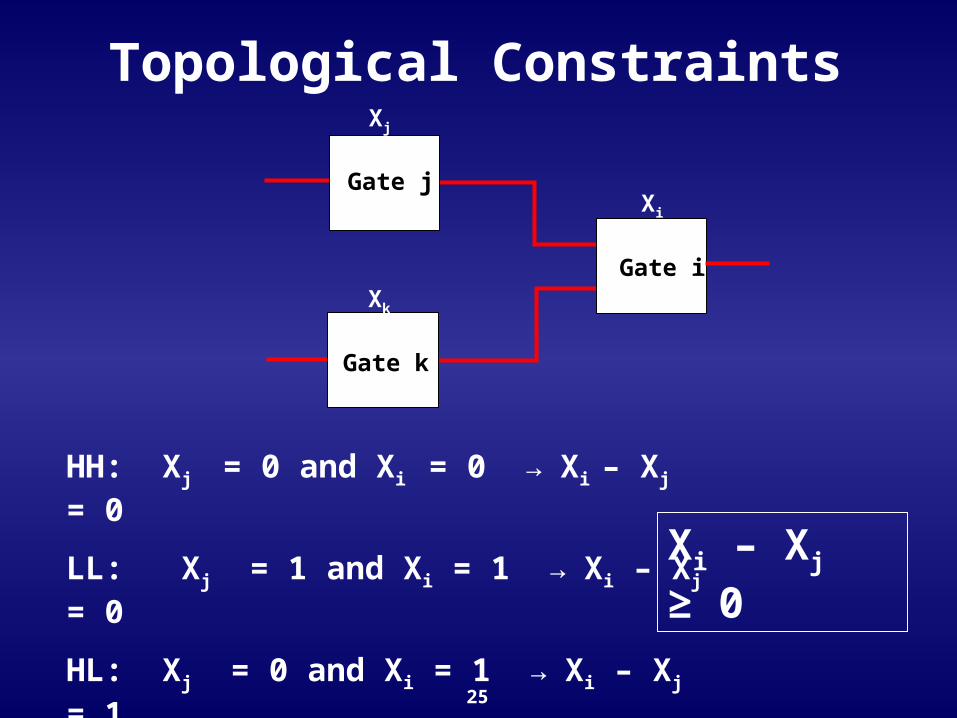
Topological Constraints
Gate i
Gate k
Gate j
Xk
Xi
Xj
HH: Xj = 0 and Xi = 0 → Xi – Xj = 0
LL: Xj = 1 and Xi = 1 → Xi – Xj = 0
HL: Xj = 0 and Xi = 1 → Xi – Xj = 1
LH: Xj = 1 and Xi = 0 → Xi – Xj = -1
Xi – Xj ≥ 0
26
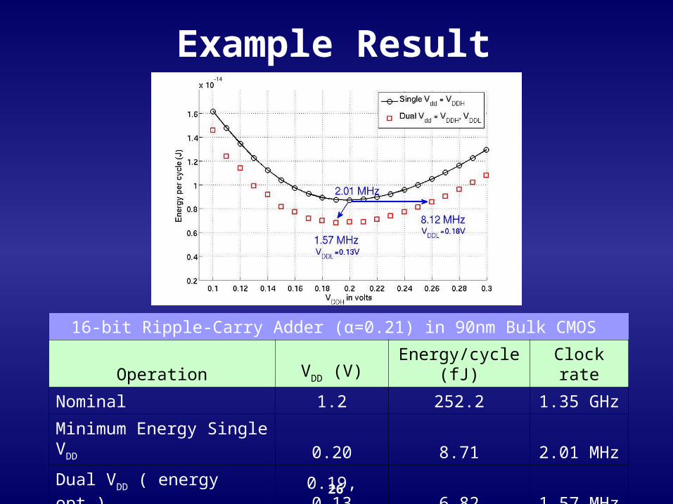
Example Result
16-bit Ripple-Carry Adder (α=0.21) in 90nm Bulk CMOS
Operation VDD (V) Energy/cycle (fJ) Clock rate
Nominal 1.2 252.2 1.35 GHz
Minimum Energy Single VDD 0.20 8.71 2.01 MHz
Dual VDD ( energy opt.) 0.19, 0.13 6.82 1.57 MHz
Dual VDD ( perf. opt.) 0.26, 0.18 8.55 8.12 MHz
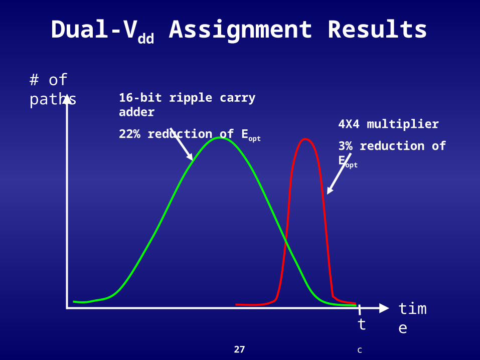
27
Dual-Vdd Assignment Results
tc
time
# of paths16-bit ripple carry adder
22% reduction of Eopt 4X4 multiplier
3% reduction of Eopt
28
Outline
• Study of Subthreshold Voltage Operation • Dual Voltage Assignment Algorithm (MILP) • Current Progress & Future Work• Conclusion
29
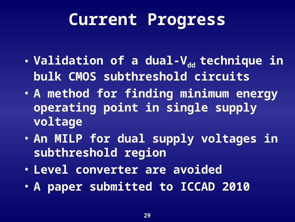
Current Progress
• Validation of a dual-Vdd technique in bulk CMOS subthreshold circuits
• A method for finding minimum energy operating point in single supply voltage
• An MILP for dual supply voltages in subthreshold region
• Level converter are avoided
• A paper submitted to ICCAD 2010
30
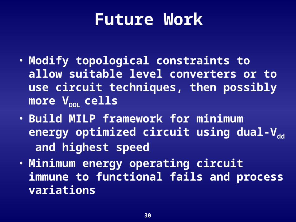
Future Work
• Modify topological constraints to allow suitable level converters or to use circuit techniques, then possibly more VDDL cells
• Build MILP framework for minimum energy optimized circuit using dual-Vdd and highest speed
• Minimum energy operating circuit immune to functional fails and process variations
31
Outline
• Study of Subthreshold Voltage Operation • Dual Voltage Assignment Algorithm (MILP) • Current Progress & Future Work• Conclusion
32
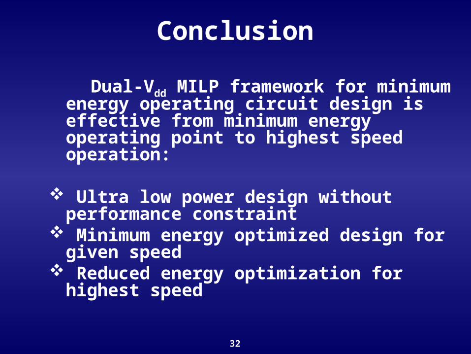
Conclusion
Dual-Vdd MILP framework for minimum energy operating circuit design is effective from minimum energy operating point to highest speed operation:
Ultra low power design without performance constraint
Minimum energy optimized design for given speed
Reduced energy optimization for highest speed
33
Thanks!