Embed Size (px)
Citation preview

Ultra-low power circuits based on tunnel FETs for energy harvesting applications
by David Cavalheiro
ADVERTIMENT La consulta d’aquesta tesi queda condicionada a l’acceptació de les següents condicions d'ús: La difusió d’aquesta tesi per mitjà del r e p o s i t o r i i n s t i t u c i o n a l UPCommons (http://upcommons.upc.edu/tesis) i el repositori cooperatiu TDX ( h t t p : / / w w w . t d x . c a t / ) ha estat autoritzada pels titulars dels drets de propietat intel·lectual únicament per a usos privats emmarcats en activitats d’investigació i docència. No s’autoritza la seva reproducció amb finalitats de lucre ni la seva difusió i posada a disposició des d’un lloc aliè al servei UPCommons o TDX.No s’autoritza la presentació del seu contingut en una finestra o marc aliè a UPCommons (framing). Aquesta reserva de drets afecta tant al resum de presentació de la tesi com als seus continguts. En la utilització o cita de parts de la tesi és obligat indicar el nom de la persona autora.
ADVERTENCIA La consulta de esta tesis queda condicionada a la aceptación de las siguientes condiciones de uso: La difusión de esta tesis por medio del repositorio institucional UPCommons (http://upcommons.upc.edu/tesis) y el repositorio cooperativo TDR (http://www.tdx.cat/?locale-attribute=es) ha sido autorizada por los titulares de los derechos de propiedad intelectual únicamente para usos privados enmarcados en actividades de investigación y docencia. No se autoriza su reproducción con finalidades de lucro ni su difusión y puesta a disposición desde un sitio ajeno al servicio UPCommons No se autoriza la presentación de su contenido en una ventana o marco ajeno a UPCommons (framing). Esta reserva de derechos afecta tanto al resumen de presentación de la tesis como a sus contenidos. En la utilización o cita de partes de la tesis es obligado indicar el nombre de la persona autora.
WARNING On having consulted this thesis you’re accepting the following use conditions: Spreading this thesis by the i n s t i t u t i o n a l r e p o s i t o r y UPCommons (http://upcommons.upc.edu/tesis) and the cooperative repository TDX (http://www.tdx.cat/?locale-attribute=en) has been authorized by the titular of the intellectual property rights only for private uses placed in investigation and teaching activities. Reproduction with lucrative aims is not authorized neither its spreading nor availability from a site foreign to the UPCommons service. Introducing its content in a window or frame foreign to the UPCommons service is not authorized (framing). These rights affect to the presentation summary of the thesis as well as to its contents. In the using or citation of parts of the thesis it’s obliged to indicate the name of the author.

Ultra-Low Power Circuits based on Tunnel FETs
for Energy Harvesting Applications
by
David Cavalheiro
Thesis submitted in partial fulfillment of the requirement
for the PhD Degree issued by the
Universitat Politècnica de Catalunya,
in its Electronic Engineering Program
Thesis advisors:
Dr. Francesc Moll
Dr. Stanimir Valtchev
Barcelona, March 2017


iii
Dedicado à Susana pela fonte inesgotável de paciência
e suporte dos últimos anos.


v
Abstract
There has been a tremendous evolution in integrated circuit technology in the past decades. With
the scaling of complementary metal-oxide-semiconductor (CMOS) transistors, faster, less power
consuming and more complex chips per unit area have made possible electronic gadgets to evolve
to what we see today.
The increasing demand in electronic portability imposes low power consumption as a key metric
to analog and digital circuit design. While dynamic power consumption decreases quadratically
with the decrease of power supply voltage, leakage power presents a limitation due to the inverse
sub-threshold slope (SS). A power supply reduction implies a consequent threshold voltage
reduction that, given the fixed SS, cause an exponential increase in leakage current. This poses a
limitation in the reduction of power consumption that is inherent to the conventional thermionic-
based transistors (MOSFETS and FinFETs). In thermionic-based transistors the SS at room
temperature is limited to 60 mV/dec.
To circumvent the SS limitation of conventional transistors, devices with different carrier
injection mechanisms independent of the thermal (Boltzmann) distribution of mobile charge carriers
are required. The Tunnel Field-Effect Transistor (TFET) is presented as the most promising post
CMOS-technology due to its non-thermal carrier injection mechanism based on Band-To-Band
Tunneling (BTBT) effect. TFETs are known as steep slope devices (SS < 60 mV/dec at room
temperature). Large current gain (ION/IOFF > 105) at low voltage operation (sub-0.25 V) and
extremely low leakage current have already been demonstrated, placing TFETs as serious
candidates for ultra-low power and energy efficient circuit applications. TFETs have been explored
mostly in digital circuits and applications.
In this thesis, the use of TFETs is explored as an alternative technology also for ultra-low power
and voltage conversion and management circuits, suited for weak energy harvesting (EH) sources.
As TFETs are designed as reverse biased p-i-n diodes (different doping types in source/drain
regions), the particular electrical characteristics under reverse bias conditions require changes in
conventional circuit topologies. Rectifiers, charge pumps and power management circuits (PMC)
are designed and analyzed with TFETs, evaluating their performance with the proposal of new
topologies that extend the voltage/power range of operation compared to current technologies and
circuit topologies. TFET-based PMCs for RF and DC EH sources are proposed and limitations
(with solutions) of using TFETs in conventional inductor-based boost converters identified.


vii
Acknowledgments
I am very grateful to my advisor Francesc Moll for the possibility of conducting research at UPC-
Barcelona under his guidance. His knowledge, experience, time and constant support were key
contributors to the realization of this thesis. I will never forget his kindness.
I would like to thank the co-advisor of this work Stanimir Valtchev. We have been collaborating
since almost a decade with success.
To the Portuguese funding institution FCT (Fundação para a Ciência e a Tecnologia), Spanish
Ministry of Economy (MINECO) and ERDF funds through project TEC2013-45638-C3-2-R
(Maragda).
To my colleagues, friends, professors and technical staff in the department of electronic engineering
that contributed with scientific discussions and support: Nivard Capdevila, Jordi Pérez, Peyman
Pouyan, Gerhard Landauer, Sergio Gómez, Martin Marietta, Mario Lanazzo, Mohamed Saad, Chen
Jin, Antonio Rubio, Antonio Calomarde, Esteve Amat, Eduard Alarcon and Santi Perez.
To the NDCL group of the Penn State University and the NIMO group from the Arizona State
University for providing the Tunnel FET and FinFET models used in the simulations of this work.
I am deeply grateful to my family, for their encouragement, love and support.
Finally, to my sweet Susana for her love, support, enormous patience and comprehension when I
had to spend long hours away from home.


ix
Contents
Abstract .......................................................................................................................................... v
Acknowledgments ........................................................................................................................ vii
Contents ........................................................................................................................................ ix
Glossary ...................................................................................................................................... xiii
List of Figures ............................................................................................................................ xvii
List of Tables ............................................................................................................................ xxiii
1. Introduction ............................................................................................................................... 1
1.1 The technology scaling roadmap so far ........................................................................... 1
1.2 New solutions for future technology nodes ..................................................................... 4
1.3 Energy Harvesting in a More than Moore era ................................................................. 5
1.4 Tunnel FETs as a key technology for Energy Harvesting............................................... 7
1.5 Thesis motivation and objectives .................................................................................... 8
1.6 Thesis organization ....................................................................................................... 10
1.7 References ..................................................................................................................... 12
2. Tunnel FET: State of the art ................................................................................................... 15
2.1 The tunneling phenomenon ........................................................................................... 15
2.2 Band-to-Band Tunneling (BTBT) current ..................................................................... 17
2.3 From tunnel diode to gated p-i-n structure .................................................................... 19
2.3.1 First observations of tunneling in gated structures .................................................... 19
2.3.2 Structure improvements for boosted performance .................................................... 21
2.3.3 Tunnel FET evolution over the past decade .............................................................. 23
2.3.4 Directions to further improvements in tunneling devices ......................................... 28

x
2.3.5 A brief discussion of the tunneling device state of the art ......................................... 29
2.4 References ..................................................................................................................... 31
3. Tunnel FET: Physical Properties ............................................................................................ 35
3.1 Thermionic injection vs. BTBT ..................................................................................... 35
3.2 Impact of physical properties in the TFET performance ............................................... 39
3.2.1 Device structure and applied model .......................................................................... 40
3.2.2 Dielectric permittivity, EOT and body thickness impact .......................................... 41
3.2.3 Impact of doping in drain and source regions of Si-TFET ........................................ 44
3.2.4 Impact of materials in a double-gate TFET ............................................................... 47
3.2.5 Impact of doping in drain and source regions for TFETs with different materials ... 48
3.3 Chapter summary .......................................................................................................... 51
3.4 References ..................................................................................................................... 52
4. Tunnel FET: Electrical Properties ........................................................................................... 53
4.1 Tunnel FET models for SPICE simulations .................................................................. 53
4.1.1 Analytic TFET model ................................................................................................ 54
4.1.2 TFET model based on look-up tables ........................................................................ 55
4.2 Electrical characteristics of TFETs ............................................................................... 56
4.2.1 Input characteristics of TFETs .................................................................................. 57
4.2.2 Output characteristics of TFETs ................................................................................ 59
4.2.3 Intrinsic capacitance of TFETs .................................................................................. 61
4.3 TFETs in digital design ................................................................................................. 62
4.4 TFETs in analog design ................................................................................................. 64
4.5 TFETs circuit layout issues and extra-parasitics ........................................................... 68
4.6 Chapter summary .......................................................................................................... 69
4.7 References ..................................................................................................................... 70
5. Tunnel FET-based Charge Pumps .......................................................................................... 73
5.1 Motivation ..................................................................................................................... 73

xi
5.2 Problems associated with TFETs in charge-pumps ...................................................... 75
5.3 Circuit-level solutions for reverse biased TFETs .......................................................... 78
5.4 Proposed TFET-based charge-pump ............................................................................. 80
5.5 Capacitance optimization of charge-pump stage........................................................... 81
5.6 Charge-pumps performance comparison ...................................................................... 84
5.7 Chapter summary .......................................................................................................... 89
5.8 References ..................................................................................................................... 90
6. Tunnel FET-based Rectifiers .................................................................................................. 91
6.1 Motivation ..................................................................................................................... 91
6.2 State of the art TFET-based Rectifier ........................................................................... 92
6.3 Advantages of Tunnel FETs in rectifiers ...................................................................... 95
6.4 Drawbacks of Tunnel FETs in rectifiers ....................................................................... 97
6.5 Proposed Tunnel FET-based rectifier ........................................................................... 98
6.6 Optimization of proposed rectifier .............................................................................. 100
6.7 Performance comparison of rectifiers ......................................................................... 102
6.8 Chapter summary ........................................................................................................ 104
6.9 References ................................................................................................................... 105
7. TFET-based Power Management Circuit for RF Energy Harvesting ................................... 107
7.1 Motivation ................................................................................................................... 107
7.2 Challenges in RF power transport ............................................................................... 108
7.3 Proposed TFET-based PMC ....................................................................................... 112
7.3.1 Startup Circuit ......................................................................................................... 113
7.3.2 Boost Circuit ........................................................................................................... 115
7.3.2.1 Challenges in TFET-based boost converter design ............................................. 117
7.3.2.2 Advantages of TFETs in PMC and boost converters .......................................... 118
7.3.3 Controller Circuit .................................................................................................... 119
7.4 Simulation Results ...................................................................................................... 122

xii
7.5 Chapter summary ........................................................................................................ 126
7.6 References ................................................................................................................... 127
8. TFET-based Power Management Circuit for nano-Watt DC Energy Harvesting sources .... 129
8.1 Motivation ................................................................................................................... 129
8.2 Proposed TFET-based PMC for ultra-low power DC sources .................................... 130
8.2.1 Startup Circuit ......................................................................................................... 131
8.2.2 Boost Circuit ............................................................................................................ 132
8.2.3 Controller Circuit .................................................................................................... 135
8.3 Simulated Results ........................................................................................................ 138
8.4 Impact of TFET-based circuit layout and parasitics .................................................... 144
8.5 Chapter summary ........................................................................................................ 144
8.6 References ................................................................................................................... 145
9. Final conclusions ................................................................................................................... 147
9.1 Summary of thesis contributions ................................................................................. 149
9.2 Future work ................................................................................................................. 150
Publications ................................................................................................................................ 151
Journals .................................................................................................................................. 151
Conferences ............................................................................................................................ 151
Workshops.............................................................................................................................. 152

xiii
Glossary
– Wavelength of transmitted signal
– Screening length
AC – Alternate Current
Al – Aluminum
Al2O3 – Aluminum Oxide
BTBT – Band-to-Band Tunneling
CC – Coupling Capacitor
CDEP – Depletion capacitance
CGD – Gate-to-Drain capacitance
CGS – Gate-to-Source capacitance
CINT – Interface capacitance
CL – Load capacitance
CMOS – Complementary Metal Oxide Semiconductor
CNT – Carbon Nano Tube
COX – Oxide capacitance
DC – Direct Current
DCM – Discontinuous Conduction Mode
DG – Double-Gate
DOS – Density of States
E – Energy
EF – Energy Fermi level
EG – Energy bang Gap
EH – Energy Harvesting
EOT – Equivalent Oxide Thickness
F – Electric field
Fc – Fermi Dirac distribution of conduction band
FDSOI – Fully Depleted Silicon on Insulator
FH – Fin Height
fMAX – Maximum oscillation frequency

xiv
FOM – Figure of Merit
fs – Boost frequency
fT – Cut-off frequency
FV – Fermi Dirac distribution of valence band
FW – Fin Width
GAA – Gate All Around
GaAs – Gallium Arsenide
GBTBT – Band-to-Band Tunneling generation rate
GBW – Gain Bandwidth Product
GCCCP – Gate cross-Coupled Charge Pump
GCCR – Gate Cross-Coupled Rectifier
Ge – Germanium
GeOI – Germanium on Insulator
GFETs – Graphene Field Effect Transistor
gm – Transconductance
gm/IDS – Transconductance efficiency
GR – Receiver antenna gain
GT – Transmitter antenna gain
HfO2 – Hafnium Oxide
HP – High Performance
HTFET – Heterojunction TFET
IC – Integrated Circuit
IE –Esaki tunneling current
InAs – Indium Arsenide
InGaAs – Indium Gallium Arsenide
IoT – Internet of Things
ISM – Industry-Science-Medical
IZ – Zener tunneling current
k (x) – Quantum wave vector
LG – Gate length
LP – Low Performance
LS – Level Shifter
LSTP – Low Standby power
LUT – Look-Up Table

xv
m* – Effective mass of the carrier
MBE – Molecular Beam Epitaxy
MM – More Moore
MoS2 – Molybdenum Disulfide
MOSFET – Metal Oxide Semiconductor Field Effect Transistor
MPPT – Maximum Power Point Tracking
MtM – More than Moore
NA – Source doping concentration
NC – Density of states in conduction band
ND – Drain doping concentration
NDR – Negative Differential Resistance
NFIN – Number of Fins
NMOS – N-type MOSFET
NO – Non-Overlapped
NV – Density of states in valence band
NW – Nano Wire
PCE – Power Conversion Efficiency
PMC – Power management Circuit
PMOS – P-type MOSFET
PR – Received power
PT – Transmitted power
PTM – Predictive Technology Model
PV – Photovoltaic
R – Propagation distance between transmitter and receiver
RA – Real part of antenna impedance
RD – Drain resistor
RF – Radio-Frequency
RG – Gate resistor
RL – Output load
RS – Source resistor
SCTJ – Surface Channel Tunnel Junction
SG – Single Gate
Si - Silicon
SiGe –Silicon-Gemanium

xvi
SiO2 – Silicon-Oxide
SOI – Silicon on Insulator
SPICE – Simulation Program with Integrated Circuit Emphasis
SS – Inverse sub-threshold slope
SSM – Self-Sustaining Mode
STT – Surface Tunnel Transistor
TAT – Trap-Assisted Tunneling
TBTBT – Tunneling transmission probability
TCAD – Technology Computer-Aided Design
tCH – Channel thickness
TEG – Thermo-Electric Generator
TFET – Tunnel Field Effect Transistor
TiN – Titanium Nitride
tOX – Oxide thickness
U –Barrier potential
UHF – Ultra-High Frequency
UTB – Ultra Thin Body
VA – Peak amplitude of the antenna
VDD – Power Supply Voltage
VDS – Drain-to-Source Voltage
VGS – Gate-to-Source Voltage
VLSI – Very Large Scale Integration
VOC –Open Circuit Voltage
VTH – Threshold Voltage
VTHD – Drain Threshold Voltage
WFIN – FinFET channel width
WKB – Wentzel-Kramers-Brillouin
ZrO2 – Zirconium Dioxide
α – Switching activity factor
εr – Relative permittivity or dielectric constant
– Natural length
Ψ – Wave function of carrier
– Reduced Planck constant

xvii
List of Figures
Fig. 1.1 Static and dynamic power dissipation trend in function of technology gate length. Source: ITRS 2015
[11].____________________________________________________________________________________ 2
Fig. 1.2 Technology Scaling Roadmap: before, now and then. ______________________________________ 3
Fig. 1.3 Integration of More Moore, More than Moore and Energy Harvesting for IoT sensors. __________ 6
Fig. 1.4 Voltage trend of logic technology. Source: ITRS 2015 [11]. __________________________________ 8
Fig. 1.5 MOSFET and Tunnel FET input characteristics. ___________________________________________ 8
Fig. 1.6 Structure of the thesis. _____________________________________________________________ 11
Fig. 2.1 Description of the tunneling effect in a diode with heavily doped p-n junctions. (a) Band-to-Band
Tunneling (BTBT) current resultant from reverse biased diode; (b) thermal equilibrium; (c) BTBT current
resultant from forward biased diode; (d) Decrease of BTBT current; (e) Diffusion and excess current with no
BTBT effect. Adapted from [3]. _____________________________________________________________ 16
Fig. 2.2 Wave function showing carrier tunneling through de barrier. Adapted from [3]. _______________ 17
Fig. 2.3 The triangular potential barrier seen by the tunneling carrier. ______________________________ 17
Fig. 2.4 Structure and energy band comparison between MOSFET and SCTJ. ________________________ 20
Fig. 2.5 Schematic view of the vertical Esaki-tunneling field effect transistor (Esaki-FET). Adapted from [13].
______________________________________________________________________________________ 22
Fig. 2.6 CNT-based TFET, adapted from [17]. __________________________________________________ 23
Fig. 2.7 Single gate and double gate structure TFET with high-k gate dielectric. Adapted from [18]. ______ 23
Fig. 2.8 Energy band cross section of the TFET. ________________________________________________ 24
Fig. 2.9 Schematic of InGaAs-TFET. Adapted from [24]. __________________________________________ 26
Fig. 2.10 Chronogram with the most important achievements of tunneling devices. __________________ 27
Fig. 2.11 Performance comparison between silicon-based (Si) and groups III-V TFETs. _________________ 28
Fig. 3.1 Double-gate TFET and double-gate MOSFET structure. ___________________________________ 35
Fig. 3.2 Energy band diagram of n-MOSFET and resultant IDS-VGS characteristics. _____________________ 36
Fig. 3.3 Band diagram of electron and hole BTBT in respective n and p-type TFETs and resulting IDS-VGS
characteristics. __________________________________________________________________________ 37
Fig. 3.4 Energy band diagrams of n-type TFETs showing leakage mechanism during the off-state. (a)
Shockley-Read-Hall generation in the source (p+) and drain (n
+) regions; (b) direct and defect-assisted
tunneling; (c) hole injection at the drain-channel interface. Adapted from [2]. _______________________ 39
Fig. 3.5 Structure of simulated n-type double-gate Tunnel FET. ___________________________________ 40
Fig. 3.6 Schematic of non-local BTBT calculation range. Adapted from [5]. __________________________ 40
Fig. 3.7 Impact of oxide material on the input characteristics of the Si-TFET at room temperature. ______ 41

xviii
Fig. 3.8 Impact of oxide thickness (considering HfO2) on the input characteristics of the Si-TFET at room
temperature. ____________________________________________________________________________ 42
Fig. 3.9 Impact of body thickness on the input characteristics of the Si-TFET at room temperature. ______ 43
Fig. 3.10 (a) Impact of drain doping on the input characteristics of the Si-TFET and (b) respective energy band
diagram. ________________________________________________________________________________ 44
Fig. 3.11 Impact of source doping on the input characteristics of the Si-TFET at room temperature. ______ 45
Fig. 3.12 Impact of source doping concentration on the energy band gap (a) and (b) and electric field (c) and
(d) considering NA=1×10²⁰
cm-3
and NA=1×10¹⁹
cm-3
and the TFET device in on-state (VDS=VGS=1V). _______ 45
Fig. 3.13 Impact of source doping in the output characteristics of the Si-TFET at room temperature. ______ 46
Fig. 3.14 Impact of materials in the input characteristics of the DG-TFETs with different materials at room
temperature. ____________________________________________________________________________ 48
Fig. 3.15 Impact of source doping concentration for different TFET materials in the internal resistance of the
device, considering VGS=2VDS and a drain doping concentration of ND=1×10¹⁸
cm-3
. ____________________ 49
Fig. 3.16 Impact of drain doping concentration for different TFET materials in the internal resistance of the
device, considering VGS=2VDS and a source doping concentration of NA=1×10²⁰
cm-3
. ___________________ 50
Fig. 3.17 Energy band diagram for (a) Ge-TFET and (b) InGaAs-TFET for a reverse biased TFET. ___________ 50
Fig. 4.1 Regions of operation in n-TFET._______________________________________________________ 53
Fig. 4.2 TFET equivalent circuit. Adapted from [1]. ______________________________________________ 54
Fig. 4.3 Comparison between modeled and simulated input and output characteristics of a double-gate InAs
TFET [4] and broken gap AlGaSb/InAs TFET [5]. _________________________________________________ 55
Fig. 4.4 Input characteristics of (a) n-type FinFET and (b) p-type FinFET configurations. _________________ 58
Fig. 4.5 Input characteristics of DG InAs-based TFET (Homojunction) for (a) n-type and (b) p-type
configurations. ___________________________________________________________________________ 58
Fig. 4.6 Input characteristics of DG GaSb-InAs-based TFET (Heterojunction) for (a) n-type and (b) p-type
configurations. ___________________________________________________________________________ 58
Fig. 4.7 Comparison of output characteristics for n-type devices considering (a) VGS=0.5 V and (b) VGS=0.2 V.
_______________________________________________________________________________________ 60
Fig. 4.8 Negative differential resistance (NDR) at negative VDS for (a) Het. n-TFET and (b) Hom. n-TFET. ____ 60
Fig. 4.9 Gate to drain (a) and gate to source (b) intrinsic capacitances of homojunction and heterojunction
TFETs. __________________________________________________________________________________ 61
Fig. 4.10 Inverter circuit configuration designed with heterojunction TFETs and transient output response. 63
Fig. 4.11 Performance comparison of an inverter designed with heterojunction and homojunction TFETs
(normalized to the performance of FinFET-based inverter). (a) Dynamic, (b) Static, (c) load capacitance and
delay (50%) and (d) total energy per clock transition. ____________________________________________ 64

xix
Fig. 4.12 Comparison of analog figures of merit between Si-FinFET and heterojunction TFET. (a)
Transconductance; (b) Transconductance per current ratio; (c) second and (d) third derivatives of current
normalized to gm. _______________________________________________________________________ 65
Fig. 4.13 Output resistance of (a) Heterojunction TFET and (b) Si-FinFET; intrinsic gain of (c) Heterojunction
TFET and (d) Si-FinFET. ____________________________________________________________________ 67
Fig. 4.14 Unity gain frequency comparison of Heterojunction TFET and Si-FinFET. ____________________ 67
Fig. 4.15 (a) Vertical TFET structure, adapted from [27]. (b) Additional contact region of TFETs due to non-
sharing possibility of drain-source regions. ___________________________________________________ 68
Fig. 5.1 (a) Conventional charge pump topology; (b) State-of-the-art (SOA) TFET-based charge-pump [7] and
(c) Regions of operation. __________________________________________________________________ 75
Fig. 5.2 TFET energy band diagram of an n-TFET under reverse bias conditions: (a) reverse BTBT mechanism,
(b) drift-diffusion mechanism. ______________________________________________________________ 76
Fig. 5.3 Reverse current comparison of (a) heterojunction n-TFET and (b) homojunction n-TFET during
reverse bias state. _______________________________________________________________________ 77
Fig. 5.4 Solution for n and p-type TFETs in GCCCP and respective transient behavior. _________________ 79
Fig. 5.5 Proposed TFET-based charge-pump. __________________________________________________ 80
Fig. 5.6 Transient behavior of the proposed TFET-based CP with heterojunction III-V TFETs considering IOUT=1
µA, WM1-4=1µm, Waux=100 nm, f=100 MHz, CL=CC=1 pF, Caux=0.1 pF, VDD=160 mV. _______________ 81
Fig. 5.7 Characteristics of Clock 1 and Clock 2. _________________________________________________ 82
Fig. 5.8 Power conversion efficiency of HTFET-Prop. Cp with one-stage as function of load capacitor. ____ 83
Fig. 5.9 Power conversion efficiency of HTFET-Prop. CP with one-stage as function of coupling capacitors. 83
Fig. 5.10 Electrical characteristics of the MPG-D655, U=80mV/K (Tamb=25 ºC). RTH=22 K/W, Relec=210 Ω. 84
Fig. 5.11 Performance comparison of charge-pumps (1 stage) considering a clock frequency of 1 KHz.
CC=CL=100 nF. TFET-based charge-pumps: WM1-M4=1 µm, Waux=0.1 µm, Caux=10 nF. FinFET-based
charge-pump: Nfins M1-M4=14. ____________________________________________________________ 86
Fig. 5.12 Performance comparison of charge-pumps (1 stage) considering a clock frequency of 100 MHz.
CC=1 pF, CL=10 pF. TFET-based charge-pumps: WM1-M4=1 µm, Waux=0.1 µm, Caux=0.1 pF. FinFET-based
charge-pump: Nfins M1-M4=14. ____________________________________________________________ 87
Fig. 5.13 Distribution of power losses in the charge pumps for clock frequency of 1 kHz and 100 MHz and
load of 1µA. ____________________________________________________________________________ 88
Fig. 6.1 (a) Conventional gate cross-coupled rectifier (GCCR) and (b) its two different regions of operation. 92
Fig. 6.2 Transient behavior of RF+ and RF- nodes. ______________________________________________ 93
Fig. 6.3 Performance comparison of a TFET-based GCCR considering 1 stage. ________________________ 95
Fig. 6.4 Reverse current of T1 during interval t3→t4, t5→ t6 for: (a) n-type heterojunction TFET and (b) n-
type FinFET. ____________________________________________________________________________ 96

xx
Fig. 6.5 Current and power consumption of transistor T1 in the GCCR during region II of operation.
Simulation conditions: VAC=0.4 V, f=915 MHz, CC=1pF, CL=10 pF, RL=100 kΩ. WT1-HTFET=1µm, NFINS-
FinFET=14. ______________________________________________________________________________ 97
Fig. 6.6 Increase of reverse losses as function of RF VAC magnitude. ________________________________ 98
Fig. 6.7 Proposed TFET-based rectifier ________________________________________________________ 98
Fig. 6.8 Active transistors in (a) first and (b) second regions of operation ____________________________ 99
Fig. 6.9 Ideal transient behavior of proposed TFET-rectifier. _______________________________________ 99
Fig. 6.10 Performance of the proposed rectifier considering (a) f=915 MHz and (b) f=100 MHz. _________ 101
Fig. 6.11 Reverse losses of rectifiers (1 stage) as function of VAC magnitudes considering (a) f=915 MHz
(prop. Rect: Wm/Wa=10) and (b) f=100 MHz (prop. Rect: Wm/Wa=5). _____________________________ 101
Fig. 6.12 Gate voltage applied to the main transistors T1 to T4 in the proposed rectifier for: a) f=915MHz
(Wm/Wa=10), b) f=100MHz (Wm/Wa=5). ____________________________________________________ 102
Fig. 6.13 Performance comparison of rectifiers for two frequencies of operation. ____________________ 103
Fig. 7.1 RF Power Transport System. ________________________________________________________ 108
Fig. 7.2 (a) Received power and (b) peak amplitude of the antenna as a function of propagation distance for
PT = 4 W. _______________________________________________________________________________ 109
Fig. 7.3 Comparison of (a) CMOS rectifiers from literature and (b) rectifier output voltage as function of
available power. ________________________________________________________________________ 110
Fig. 7.4 (a) Equivalent circuit of antenna-matching-rectifier and (b) TFET-based GCCR topology. ________ 110
Fig. 7.5 (a) Rectifier efficiency as function of available power considering different technologies; (b)
Heterojunction TFET-based rectifier PCE as a function of output load; (c) Rectifier output power as a function
of output voltage for heterojunction TFET-based rectifier. _______________________________________ 111
Fig. 7.6 Proposed RF TFET-based Power Management Circuit for energy harvesting applications. _______ 112
Fig. 7.7 Digital and analog circuitry of the startup module. _______________________________________ 113
Fig. 7.8 (a) Voltage reference and (b) comparator circuit topologies applied in the voltage monitor block of
startup circuit. __________________________________________________________________________ 114
Fig. 7.9 Proposed boost converter topology for TFET devices. ____________________________________ 115
Fig. 7.10 Transient behavior of the main electrical signals when the boost controller is enabled. ________ 116
Fig. 7.11 (a) Top: CBOOST charging from rectifier; Middle: Inductor charging from CBOOST; Bottom: Inductor
discharging to COUT; (b) Reverse current for different technologies as a function of VDS in S4. __________ 118
Fig. 7.12 Internal resistance of different technologies (n-type) under reverse (VDS < 0V) and forward (VDS >
0V) bias. FinFETs under reverse bias present VGS=VDS, whereas for TFET VGS=0V. ___________________ 119
Fig. 7.13 Proposed TFET-based controller circuit applied to the boost converter. _____________________ 120
Fig. 7.14 (a) Vx_aux generator circuit and (b) Level shifter (LS) circuit block. _________________________ 120

xxi
Fig. 7.15 Increase of current consumption in digital cells for non-matched input (VIN) and power supply
voltage (VDD=0.2 V). ____________________________________________________________________ 121
Fig. 7.16 Increase of current consumption in inverter cells for non-matched input (VIN) and power supply
voltage. _______________________________________________________________________________ 121
Fig. 7.17 Transient simulation of the proposed TFET-based PMC for RF Pav= -25 dBm. L1=10 mH,
CBOOST=0.05 µF, COUT=0.05 µF, CSNUB=2 nF, RL=166.7 kΩ, WS1=10 µm, WS2,3,5=100 µm, WS4=25 µm.
_____________________________________________________________________________________ 123
Fig. 7.18 Performance of TFET-based boost converter for RF Pav= -25 dBm. Cout=Cboost, Csnub=2 nF,
Rload=166.7 kΩ, WS1=10 µm, WS2,3,5=100 µm. ______________________________________________ 124
Fig. 7.19 Distribution of power losses in the PMC for RF Pav= -25 dBm. L1=10 mH, CBOOST=0.05 µF,
COUT=0.05 µF, CSNUB=2 nF, RL=166.7 kΩ, WS1=10 µm, WS2,3,5=100 µm, WS4=25 µm. _____________ 125
Fig. 8.1 Top level architecture of the proposed TFET-based PMC for ultra-low voltage/power DC sources. 130
Fig. 8.2 Digital and Analog circuitry of the proposed TFET-based startup circuit. _____________________ 131
Fig. 8.3 (a) Comparator circuit topology and (b) voltage reference applied in the voltage monitor block of
startup circuit. _________________________________________________________________________ 132
Fig. 8.4 Conventional and (b) proposed TFET-based boost converter. _____________________________ 133
Fig. 8.5 (a) Operation states of the proposed TFET-based boost converter; (b) Operation sequence of the
main electrical signals applied to the proposed boost converter. _________________________________ 134
Fig. 8.6 Proposed TFET-based controller circuit for the boost converter. ___________________________ 135
Fig. 8.7 Circuits of Clock and Phase 1 signals. _________________________________________________ 136
Fig. 8.8 Proposed TFET-based voltage divider charge pump. _____________________________________ 137
Fig. 8.9 (a) Clock frequency in function of Cosc; (b) Phase 1 time required for MPPT. L=470 µH, f=100Hz. 138
Fig. 8.10 Performance of the conventional and proposed TFET-based boost converters considering a DC
energy harvesting source with 1MΩ. LBOOST=470 µH, WS1=5µm, WS2=1mm, WS3=10µm, WS5=50µm.
WS6=200µm, __________________________________________________________________________ 139
Fig. 8.11 Distribution of power losses in the proposed TFET-based startup and controller circuits. ______ 140
Fig. 8.12 Performance of the proposed TFET-based boost converter for different voltage conversion ratios.
WS4=200 µm (WS4_1=WS4_2=100 µm). ____________________________________________________ 141
Fig. 8.13 Distribution of power losses in the proposed boost-converter for different voltage conversion ratios
(VIN=0.1 V, VOUT=0.5V, 0.6V and 0.7V) considering an output load of 100 nA (PIN= 10 nW) and 1µA (for PIN=
100 nW). ______________________________________________________________________________ 142
Fig. 8.14 Load ON-time for different input power levels and output voltage. _______________________ 142
Fig. 8.15 TFET-based PMC transient behavior considering PIN=10 nW, VIN=0.1 V, VOUT=0.5 V, RL=25 MΩ, L=470
µH, __________________________________________________________________________________ 143


xxiii
List of Tables
Table 2.1 Natural length for different device configurations. From [19]. ____________________________ 24
Table 4.1 Physical parameters of the double-gate Tunnel FETs modeled by the look-up tables. ________ 56
Table 5.1 Bias conditions of the TFETs applied in the GCCCP considering Region I. ___________________ 76
Table 5.2 Bias conditions of the TFETs applied in the GCCCP considering Region II. ___________________ 76
Table 5.3 VGS bias of the proposed TFET-based charge-pump. ____________________________________ 81
Table 5.4 Suitable charge-pump topology for different voltage/power range.________________________ 89
Table 6.1 Steady-state bias conditions of the TFET-GCCR in region I. _______________________________ 94
Table 6.2 Steady-state bias conditions of the TFET-GCCR in region II._______________________________ 94
Table 6.3 Ideal VGS conditions of the proposed rectifier in both regions of operation (bold: transistors in off-
state) _________________________________________________________________________________ 100
Table 6.4 Suitable rectifier topology for different voltage/power range. ___________________________ 104
Table 7.1 Frequency Band allocations and maximum transmitter power [1].________________________ 109
Table 7.2 Performance comparison of the proposed TFET-PMC with state of the art. ________________ 125
Table 8.1 Bias condition of TFETs applied to the voltage divider CP in steady state conditions. _________ 137
Table 8.2 Performance comparison with power management circuits from the literature. ____________ 143


1
Chapter 1
1. Introduction
1.1 The technology scaling roadmap so far
Since 1947 with the invention of the first transistor by William Shockley, John Bardeen and
Walter Brattain at Bell Labs [1] and the Integrated Circuit (IC) at Texas Instruments by Jack Kilby
in 1958 [2], the impact of the electronic technology evolution in our daily activities has been so
enormous that nowadays it is unthinkable to live without it. Smart-cars, smart-phones, smart-
watches, smart-TVs and healthcare gadgets are just a few examples that ease our daily life, mainly
due to the downscale evolution of the electronic transistor. The exponential growth of the transistor
number on a die, following Moore’s law [3] has been the major impulse for the semiconductor
industry over the years. The decrease of the technology node and consequent transistor channel
length has led to the possibility of adding more devices on a single die, thus reducing the production
cost of a chip and increasing its complexity. Also, the reduction of the transistor size allowed the
design of faster circuits with reduced power consumption (per transistor).
Until the late 90’s, the transistor scaling theory of Dennard’s, 1974 [4], was well followed by the
semiconductor industry, i.e. the power supply voltage VDD and threshold voltage VTH of the
transistor decreased linearly with the reduction of the channel length and width dimensions.
Consequently, with the decrease of VDD a quadratic decrease of the dynamic power consumption in
the transistor and hence in the IC was observed over the years. The successful downscaling of the
transistors was mainly achieved due to the excellent material and electrical properties of the SiO2,
the material used in the dielectric between the gate and the channel of the device.
During the past 15 years, several modifications in the transistor structure were required in order
to keep the technology downscaling trend. As an example, strained silicon technology was

Chapter 1. Introduction
________________________________________________________________________________
2
implemented in the 90 nm technology node in order to improve the carrier mobility inside the
transistor. This was done by some approaches such as embedding SiGe materials in the PMOS
source/drain regions and tensile silicon nitride-capping layer for NMOS devices [5]. With reduced
gate oxide thickness, the increase of gate leakage due to current flowing through the thin gate
insulator (by tunneling) was presented as the major problem to be solved at 45 nm technology
nodes. The introduction of gate dielectrics with large dielectric constant (εr ≈ 25 for HfO2 compared
to that of SiO2, ε ≈ 3.9) significantly reduced the gate leakage, thus allowing the decrease of the
technology node down to 32 nm [6]. With further reduction of channel length, the increase of
thermal diffusion of carriers and consequent increase of leakage current required changes in the
conventional bulk-CMOS structure. To overcome the consequent increase of static power
consumption in chips, different device structures such as Fully Depleted Silicon on Insulator
(FDSOI) and FinFETs were developed and are currently under production with technology nodes as
low as 7 nm [7].
FinFETs are known as multi-gate devices. They are characterized by a gate electrode wrapped
around several sides of the conducting channel, replacing the planar configuration of the
conventional single-gate MOSFETs. Transistors with multi-gate configuration increase the
electrostatic control of the gate over the channel, thus allowing the reduction of short channel
effects and consequent reduction of leakage power inside the device [8].
Fig. 1.1 Static and dynamic power dissipation trend in function of technology gate length. Source: ITRS 2015 [11].
8
12
16
20
24
28
32
1E-01
1E+00
1E+01
1E+02
1E+03
1E+04
1E+05
2013 2015 2017 2019 2021 2023 2025 2027
Ph
ysic
al g
ate
len
gth
(n
m)
No
rmal
ized
ch
ip p
ow
er d
issi
pat
ion
(to
20
15
)
Year
Static Power Trend
Dynamic Power
HP LP
Lg
New Structures and Transport Scheme

Chapter 1. Introduction
________________________________________________________________________________
3
Fig. 1.2 Technology Scaling Roadmap: before, now and then.
FDSOI devices are characterized by an ultra-thin layer of insulator placed on top of the silicon
base and below a non-doped thin silicon-based channel. Despite the superior electrostatic control of
the gate over the channel compared to bulk-CMOS, FDSOI allows the modulation of the threshold
voltage VTH of the device by changing the polarity of the body bias [9].
As shown in Fig. 1.1, during the next few years transistors are expected to be reduced to a few
nanometers, and further miniaturization of the transistor will be practically impossible [10]. As the
dimensions of MOSFETs are approaching a scale at which they will be composed of just a few

Chapter 1. Introduction
________________________________________________________________________________
4
hundred atoms, undesirable effects such as gate tunneling will prevent further improvements in the
device performance due to large leakage currents. In order to avoid the consequent increase of static
power trend of chips with further technology downscale and keep the increase of transistor density
with a viable economical production, the semiconductor industry will eventually push efforts in the
development of vertical device geometries, circuitry with multiple layers (3D integration) and
different electrical transport schemes [11]. In order to accomplish this, the development of devices
with alternative materials, namely SiGe, Ge and compounds drawn from groups III-V of the
periodical table is mandatory. To summarize, Fig. 1.2 presents the CMOS technology scaling
roadmap so far, and emerging devices under research for further miniaturization of transistors.
1.2 New solutions for future technology nodes
In order to face the increase of static power consumption trend in chips for future technology
nodes, changes in the channel material/structure are required [11]. The most promising technologies
to keep the downscaling technology to few nanometers are listed below:
Ge and III-V materials: according to ITRS 2015 previsions, the next step in the scaling
roadmap will rely on the replacement of the strained silicon channel of MOSFETs by high
mobility materials [11]. This task is challenging as many factors still have to be overcome,
e.g. improvement of high-K/Ge-III-V interface, minimization of band-to-band tunneling in
narrow bandgap channel materials and very large scale integration (VLSI) using a
manufacturable process flow on a silicon platform are presented as some examples [12-13].
Nanowires (NW): the replacement of conventional planar MOSFET channels with NWs may
allow further decrease of the technology node due to the possibility to manufacture NWs
with diameters of few nanometers [14]. NWs match well with gate-all-around structures that
may enable the reduction of short channel effects. They are grown vertically benefiting
future vertical integration of devices in chips. In order to grow defect-free nanowires,
device yield and uniformity has to be improved, as well as position registry if the
transferring of NWs to a different substrate is required. In order to avoid surface roughness
and defects, proper surface treatment and passivation techniques need to be developed.
Carbon Nanotubes (CNT): with an ultra-thin body of ≈ 1 nm of diameter, CNT-FETs are
presented as a viable option for sub-10 nm technology nodes. Compared to silicon, CNTs
can offer improved electron and hole mobilities in the channel at room temperature.
Purified and sorted CNTs with relatively uniform diameter distribution are presented as
some problems that have to be overcome for VLSI integration [15].

Chapter 1. Introduction
________________________________________________________________________________
5
Graphene FETs (GFETs): with a higher carrier mobility than that of CNTs, graphene
materials can benefit the RF design community by allowing faster transistors with reduced
dimensions. As graphene is presented as a single atomic layer, it is presented as a zero
bandgap semiconductor. Therefore, the main research relies on opening a bandgap in order
to efficiently allow a large current gain (ION/IOFF) for both analog and RF applications [16].
Tunnel FETs (TFETs): the TFET is considered the most promising switching technology for
low-power, low-performance applications due to its unique electrical characteristics [17].
With a different carrier injection mechanism in comparison to conventional thermal
devices, TFETs can achieve an inverse sub-threshold slope (SS) with sub-60 mV/dec at
room temperature. With this characteristic, TFETs have the potential to achieve a low
operating voltage, maintaining a large current gain. The future integration of TFETs in low
power chips is strongly dependent on the evolution of III-V manufacturing processes as
TFETs designed with groups III and V materials overcome the electrical performance of Si-
based TFETs [18].
Further improvements in conventional transistor architectures and the integration of new
materials may not only keep the downscaling of the technology roadmap but also enhance the
functionality and performance of future electronic systems. However, as eventually the dimensional
scaling of current technology will approach fundamental limits, different trends than the current
“More Moore” (MM) will eventually emerge.
1.3 Energy Harvesting in a More than Moore era
Nowadays, the industry is pursuing a new trend denominated “More than Moore” (MtM), where
the improved performance of new technologies is not only traded against power, but also against
functional diversification of semiconductor-based devices [11]. The rise of new materials and
emerging technologies can open doors to further improvements in areas that do not necessarily scale
at the same rate than that of digital functionalities (e.g. sensors, actuators, biochips, RF, analog
design, energy harvesting, power management, Internet of Things, etc..). Therefore, the
heterojunction integration of “More Moore” (digital) and “More than Moore” (non-digital)
functionalities into compact integrated systems is expected to further improve the performance of a
wide variety of applications such as communications, healthcare, security and automotive, among
others, where the performance is not the main metric to accomplish but rather functionality.
The market of Internet of things (IoT) is one that will certainly benefit from the integration of
MM and MtM trends. The possibility of wireless interconnection of any device through the Internet

Chapter 1. Introduction
________________________________________________________________________________
6
or local networks can enable objects to be sensed/controlled remotely, creating opportunities in
several areas where systems have to perform actions or sense the surrounding environment. The IoT
market is expected to create a huge network of billions or trillions of devices communicating with
one another and therefore, for a reason of cost, availability and convenience one of the major
challenges for this system integration is the replacement of the battery by green solutions such as
energy harvesting (EH) [19].
In Fig. 1.3, a possible architecture of a self-powered sensor node, comprising “More Moore”
technologies for digital processing, “More than Moore” for sensing and power management units,
and energy harvesting for powering the whole system is considered. In order to power an integrated
system such as the one presented, or any other system with energy from the surrounding
environment, several challenges have to be solved: first, the digital processing and storage unit have
to be extremely energy efficient, requiring the lowest possible power consumption for a proper
operation. This will minimize the energy required for a proper system functioning. Second, the
power management circuit has to consume less than the power produced by the energy harvesting
transducer. This will enable the storage of energy in a charge tank to be further used as a power
supply source for the entire system.
Fig. 1.3 Integration of More Moore, More than Moore and Energy Harvesting for IoT sensors.
Surrounding Energy
Integrated System
External Environment
Power and
Power Management
Interact
Digital Processing
and Storage
External Actuation
More Moore
More than Moore
Energy Harvesting
EH Transducer

Chapter 1. Introduction
________________________________________________________________________________
7
1.4 Tunnel FETs as a key technology for Energy Harvesting
A solution to minimize the power consumption of the digital processing unit is to decrease the
power supply voltage VDD of the digital circuitry. A linear decrease of VDD will result in a quadratic
decrease of the dynamic power consumption of the digital circuitry. However, if the threshold
voltage VTH of the transistor does not scale proportionally with VDD, the leakage current and
consequent static power consumption of the system will suffer from an exponentially increase. This
is directly related to the thermal dependent carrier injection mechanism of conventional MOSFETs:
the inverse sub-threshold slope (SS) is limited by 60 mV/ dec (at room temperature), and therefore a
decrease in VDD results in an exponential increase of sub-threshold leakage current according to the
equation expressed by (1.1) [20]:
(
) (1.1)
In the sub-threshold leakage current expression, K1 and n are constants experimentally derived,
W is the width of the transistor and is the thermal voltage with a value of 25 mV at room
temperature. As shown in Fig. 1.4, the threshold voltage of transistors for both high performance
(HP) and low performance (LP) applications are expected to be maintained constant for the next
few years [11]. With the decrease of the power supply voltage VDD, an increase of leakage power in
chips will be expected as shown by the power trends shown in Fig. 1.1. With the introduction of
different technologies with new materials and transport schemes (not thermal dependent), the
reduction of the threshold voltage in the transistors will be possible without the cost of increased
static/leakage power consumption of chips.
There is currently a great research on switches with steep SS, i.e. sub-60 mV/dec (at room
temperature). Among several options and with a different carrier injection mechanism, the Tunnel
FET (TFET) device is presented as the most promising switch technology for low voltage operation
(sub-0.5 V) and low performance applications [21-22]. As presented in Fig. 1.5, the Tunnel FET
device allows for a decrease of the overdrive voltage (VGS-VTH) maintaining a superior performance
in terms of leakage current and consequent static power consumption when compared to
conventional thermal MOSFETs. With improved performance at low voltage, the TFET device is
presented as a natural candidate to be applied to ultra-low power, low-performance integrated
circuits (e.g. IoT sensor nodes) powered by the surrounding energy [11].

Chapter 1. Introduction
________________________________________________________________________________
8
Fig. 1.4 Voltage trend of logic technology. Source: ITRS 2015 [11].
Fig. 1.5 MOSFET and Tunnel FET input characteristics.
1.5 Thesis motivation and objectives
With the increased demand in electronic portability, the chip industry market is forcing “ultra-
low power” as a key metric to achieve in order to extend the battery lifetime of future electronic
gadgets, or, if possible, to use the surrounding energy as the main power source. However, this
metric contrasts with the increase of power consumption trend shown by recent technologies at
reduced dimensions. In order to avoid the increase of static power that degrades the performance of
ultra-low power circuits with reduced technology nodes, technologies with different carrier
injection mechanisms are required. The Tunnel FET (TFET) device is shown in the technology
0.0
0.1
0.2
0.3
0.4
0.5
0.6
0.7
0.8
2015 2017 2019 2021 2023 2025 2027
Vo
ltag
e (V
)
Year
VDD
VTH LP
VTH HP
III-V n-channel Ge p-chanel
TFET
Focus on power
Focus on function
Battery Battery+EH

Chapter 1. Introduction
________________________________________________________________________________
9
scaling roadmap as a candidate for future technology nodes. It can allow the reduction of both static
and dynamic power consumption in circuits due to the improved electrical characteristics at low
voltage operation. In the literature, most of the works based on TFETs are related to logic design
and techniques to improve the device performance. There are few works exploring the performance
of TFETs in analog applications, and a clear lack of works investigating the performance of this
technology in power management circuits for energy harvesting applications.
Considering the above mentioned points, this thesis aims to investigate the electrical
performance of TFET devices, exploring opportunities and drawbacks of using this emerging
technology in the design of ultra-low power circuits for energy harvesting applications. In order to
accomplish this goal, this thesis focuses on the design of TFET-based power conversion circuits and
power management circuits, exploring their limitations and providing circuit architectural solutions
to leverage on the different TFET electrical characteristics. To accomplish the objectives, several
topics are addressed as follows:
At a device level, evaluate the electrical properties of TFETs with the impact of
physical parameters: with the support of Atlas Device Simulator from Silvaco [23], the
dependence of the TFET current-voltage characteristics on the dimensions and materials
of the channel and gate dielectric has to be evaluated. This part is important as it
highlights the most important physical parameters to take into account at a device level,
for further improvements of TFET-based circuit performance.
To determine figures of merit reflecting both the digital and analog performance of
TFET devices: with an optimized TFET model for circuit simulations, a comparison
between several figures of merit between TFETs and thermionic MOSFETs, at a device
level, for both analog and digital design has to be performed. This will allow to identify
the voltage range where TFETs present improved electrical performance in comparison
to conventional technologies.
To evaluate the performance of TFET-based front-end circuits for energy
harvesting applications: as charge-pumps and rectifiers are usually the circuits
interfacing the energy harvesting transducer with the power management unit, a study
on the application of TFETs in such front-end circuits is required. This will allow to
identify the voltage/power levels where the integration of TFETs is advantageous
compared to the application of conventional thermionic MOSFETs. Advantages and
drawbacks have to be identified, with the proposal of circuit-solutions to improve the
performance of TFET-based front-end circuits.

Chapter 1. Introduction
________________________________________________________________________________
10
Propose TFET-based power management circuits (PMC) for RF and DC energy
harvesting sources: with a previous study on TFET-based circuits for both analog and
digital design, and the proposal of front-end circuits, PMCs have to be designed
considering the different electrical characteristics of this technology. Similar to the
previous point, advantages and drawbacks have to be identified, with the proposal of
circuit-solutions to further improve the performance of TFET-based PMCs.
1.6 Thesis organization
In order to accomplish the previous topics, this thesis was performed with the framework
presented in Fig. 1.6. In Chapter 2, the TFET state of the art is presented. The Band-to-Band
Tunneling (BTBT) carrier injection mechanism of TFETs is explained, and an historical review of
the TFET structure is presented.
In Chapter 3, a study on the TFET current-voltage dependence on several physical parameters is
performed. This allows to identify key parameters for enhanced TFET-based circuit performance. In
Chapter 4, optimized TFET models are simulated to compare the electrical characteristics of TFETs
and conventional thermionic MOSFETS (such as FinFETs) for digital and analog applications.
Chapter 5 and Chapter 6 perform a study on the implementation of TFETs in front-end circuits
for energy harvesting applications: charge-pumps and rectifiers. Solutions to improve the
performance of such TFET-based front-end circuits are explored and compared with conventional
circuit solutions found in the literature. These two chapters identify the range of voltage and power
levels where TFET-based converters present improved performance in comparison to that of
thermionic-based counterparts.
Chapters 7 and Chapter 8 propose TFET-based power management circuits (PMC) for energy
harvesting applications. Such circuits are designed with the previously studied TFET-based front-
end circuits (rectifier and charge-pump for RF PMC and charge-pump for DC PMC). In Chapter 7,
a PMC for µW RF energy harvesting applications is proposed, designed and optimized (considering
the particular TFET electrical characteristics) with a startup circuit, controller and boost converter.
Limitations and advantages of using TFETs in such circuits are identified. Chapter 8 is presented as
an extension of Chapter 7. With the previous limitations identified, Chapter 8 proposes solutions to
enhance the performance of the PMC at decreased power levels. A study of the proposed TFET-
based power management circuit powered by nW DC energy harvesting sources is presented.
Finally Chapter 9 concludes the work, discussing the main results and pointing directions for
future works.

Chapter 1. Introduction
________________________________________________________________________________
11
Fig. 1.6 Structure of the thesis.
Power Management Units
Front-end circuits
Tunnel FET state of the art
(Chapter 2)
Tunnel FET: Physical Properties
(Chapter 3)
TFET-based Rectifiers
(Chapter 6)
TFET-based Charge-pumps
(Chapter 5)
TFET-based PMC for RF sources
(Chapter 7)
TFET-based PMC for DC sources
(Chapter 8)
Conclusions and future work
(Chapter 9)
Tunnel FET: Electrical Properties
(Chapter 4)

Chapter 1. Introduction
________________________________________________________________________________
12
1.7 References
1 Shockley, W. “The path to the conception of the junction transistor,” IEEE Transactions on
Electron Devices, vol. 23, pp. 597–620, 1976.
2 Kilby, J. S. “Turning Potential Into Realities: The Invention of the Integrated Circuit,”
http://nobelprize.org/nobel_prizes/physics/laureates/2000/kilby-lecture.pdf, 2000.
3 Moore, G. E. “Cramming more components onto integrated circuits”, Reprinted from
Electronics, vol. 38, no.8, pp. 114-117, 1965.
4 Dennard, R. H. et al. “Design of ion-implanted MOSFET’s with very small physical
dimensions,” IEEE J. Solid-State Circuits, vol. 9, pp. 256–268, 1974.
5 Thompson, S. E. et al. “A 90-nm logic technology featuring strained-silicon,” IEEE Trans.
Electron Devices, vol. 51, no. 11, pp. 1790–1797, 2004.
6 Chau, R., et al. “High-k/metal-gate stack and its MOSFET characteristics,” IEEE Electron
Device Letters, vol. 25, no.6, pp. 408–410, 2004.
7 Wu, S. Y. et al., “A 7nm CMOS platform technology featuring 4th generation FinFET
transistors with a 0.027µm2 high density 6-T SRAM cell for mobile SoC applications," IEEE
International Electron Devices Meeting (IEDM), pp. 2.6.1-2.6.4, 2016.
8 Ferain, I., Colinge, C. A. and Colinge, J. P. “Multigate transistors as the future of classical
metal-oxide-semiconductor field-effect transistors”, Nature, vol. 479, pp. 310–316, 2011.
9 Sugii, N. “Road to Vmin=0.4V LSIs with least-variability FDSOI and back-bias control,” SOI
Conference, 2011 IEEE International, pp. 1-19, 2011.
10 Courtland, R. “Transistors could stop shrinking in 2021,” in IEEE Spectrum, vol. 53, no. 9, pp.
9-11, Sep. 2016.
11 “http://www.itrs2.net/,” International Technology Roadmap for Semi- conductors, 2015.
12 Nainai, A. et al. “Engineering of Strained III-V Heterostructures for High Hole Mobility,”
IEEE International Electron Device Meeting, pp. 1-4, 2009.
13 Tsipas, P. and Dimoulas, A., “Modeling of negative charged states at the Ge surface and
interfaces,” Appl. Phys. Lett., vol. 94, 012114, 2009.
14 Luryi, S., Xu, J. and Zaslavsky, A. “Nanowires: Technology, Physics and Perspectives,” in
Future Trends in Microelectronics: From Nanophotonics to Sensors to Energy, 1, Wiley-IEEE
Press, pp.171-181, 2010.
15 Kim, Y. “Integrated Circuit Design Based on Carbon Nanotube Field Effect Transistor,”
Transactions on electrical and electronic materials, vol. 12, no. 5, pp. 175-188, 2011.

Chapter 1. Introduction
________________________________________________________________________________
13
16 Akinwande, D., Petrone, N. and Hone, J. “Two-dimensional flexible nanoelectronics,” in
Nature communications, vol. 5, no. 5678, Dec. 2014.
17 Ionescu, A. M. and Riel, H. “Tunnel field-effect transistors as energy- efficient electronic
switches,” Nature, vol. 479, pp. 329–337, November 2011.
18 Avci, U. E., Morris, D. H. and Young, A. “Tunnel Field-Effect Transistors: Prospects and
Challenges,” in IEEE Journal of the Electron Devices Soc., vol. 3, no. 3, pp. 88-95, May 2015.
19 Chen, S., Xu, H., Liu, D., Hu, B. and Wang, H. “A Vision of IoT: Applications, Challenges,
and Opportunities With China Perspective,” in IEEE Internet of Things Journal, vol. 1, no. 4,
pp. 349-359, Aug. 2014.
20 Kim, N. S. et al., "Leakage current: Moore's law meets static power," in Computer, vol. 36, no.
12, pp. 68-75, Dec. 2003.
21 Ionescu, A. M. et al., "Ultra low power: Emerging devices and their benefits for integrated
circuits,” Electron Devices Meeting (IEDM), IEEE International, pp. 16.1.1-16.1.4, 2011.
22 Nikonov, D. E. and Young, I. A. “Uniform methodology for benchmarking beyond-CMOS
logic devices,” in Technical Digest -International Electron Devices Meeting, IEDM, pp.
25.4.1-25.4.4, 2012.
23 Atlas User’s Manual, Silvaco, Inc. Santa Clara, CA, Nov. 7, 2014.


15
Chapter 2
2. Tunnel FET: State of the art
2.1 The tunneling phenomenon
Back in 1958, the Japanese scientist L. Esaki at Sony Corporation was the first to demonstrate a
device working under the principle of Band-to-Band Tunneling (BTBT): the tunnel diode [1]. The
principle of operation based on the laws of quantum theory was shown to be different from the
transistors, ordinary diodes and other semiconductor devices of that time. In a tunnel diode, carriers
can disappear from one side of a potential barrier and appear instantaneously on the other side, even
if the carrier does not have sufficient energy to surmount the barrier. It is like the carrier can
“tunnel” underneath the barrier which is the space charge depletion region of the p-n junctions. At
first, the potential of the tunnel diode was not recognized, much due to the lack of comprehension
of the tunneling behavior. After many decades of investigation, the rich amount of information
about tunneling processes has turned the tunneling effect as a possible solution to emerging
switching devices due to advantages shown at low-voltage operation (sub-0.5 V).
During the investigation of the internal field emission in semiconductor diodes with heavily-
doped germanium (Ge) junctions, a non-monotonic current-voltage characteristic under forward
bias conditions and low temperatures was observed by L. Esaki. The elasticity of the tunneling
process using Ge materials resulted in a negative differential resistance (NDR) effect, where the
electron energy was shown to be conserved during the tunneling process. Due to the great
importance of the tunneling effect in semiconductors, L. Esaki was awarded with the Nobel Prize of
Physics in 1973. Radio transmitters and receptors, amplifiers, computation and DC to AC converters
were some of the first areas to benefit from the NDR effect in the current-voltage characteristic of
the tunnel diode [2].

Chapter 2. Tunnel FET: State of the art
________________________________________________________________________________
16
Fig. 2.1 Description of the tunneling effect in a diode with heavily doped p-n junctions. (a) Band-to-Band Tunneling
(BTBT) current resultant from reverse biased diode; (b) thermal equilibrium; (c) BTBT current resultant from forward
biased diode; (d) Decrease of BTBT current; (e) Diffusion and excess current with no BTBT effect. Adapted from [3].
In Fig. 2.1, the NDR effect in the current-voltage characteristics of a tunnel diode is presented
and explained graphically. With high doped junctions and considering thermal equilibrium, the
Fermi levels are located within the allowed bands as shown in Fig. 2.1 (b). Above the Fermi level
there are no filled states (electrons) and below the Fermi level no empty states (holes) available on
the regions [3]. When a differential of potential between regions occurs, electrons may tunnel from
the conduction band to the valence band (and vice-versa) if some conditions are verified: occupied
energy states exist on the side from which the electron tunnels; unoccupied energy states exist at the
same energy level on the side to which the electron can tunnel; the tunneling potential barrier height
is low and the barrier width is small enough that there is a finite tunneling transmission probability;
the electron energy is conserved during the tunneling process.
As shown in Fig. 2.1 (c), under a forward bias condition, energy bands exist between regions in
which there are filled states in the n-region and unoccupied states in the p-region. Therefore,
electrons can tunnel from one region to the other. As shown in Fig. 2.1 (d) and with a further
increase of forward voltage, common energy bands in both regions are getting closer and at some
voltage, no available states will exist at the opposite side and therefore no BTBT effect will occur. A
further increase of the voltage bias will lead to thermionic carrier injection where electrons can pass
over the tunneling potential barrier as shown in Fig. 2.1(e). In this case, diffusion current and excess
current start to dominate the total current. As shown in Fig. 2.1 (a), when a negative bias (reverse) is
applied to the tunnel diode, electrons can tunnel from the valence band of the p-region to the
conduction band of the n-region and the NDR effect is not observed. In the following sections, this
(a) (b (c) (d (e)
Zener
Tunneling Esaki
Tunneling
Esaki
Tunneling
Barrier
Barrier

Chapter 2. Tunnel FET: State of the art
________________________________________________________________________________
17
reverse BTBT effect will be explained in more detail as it is presented as the main carrier injection
mechanism of gated Tunnel diodes (Tunnel FETs).
2.2 Band-to-Band Tunneling (BTBT) current
In classical mechanics, carriers are confined by the potential walls between regions, and only
those with excess energy higher than the barriers can escape from one region to another by
thermionic emission. In contrast and as shown in Fig. 2.2, in quantum mechanics a carrier can be
represented by its wave function ψ that does not terminate abruptly on a wall of finite potential
height U0 and therefore there is a non-zero probability of tunneling from one region to another
through the barrier [3].
Fig. 2.2 Wave function showing carrier tunneling through de barrier. Adapted from [3].
As explained in the previous section and as shown in Fig. 2.3, in a tunneling device two types of
tunneling current can be identified: the Zener tunneling current (electrons tunneling from the
valence band to the conduction band) and the Esaki tunneling current (electrons tunneling from the
conduction band to the valence band).
Fig. 2.3 The triangular potential barrier seen by the tunneling carrier.
In a tunneling device, the current is dependent on the tunneling transmission probability TBTBT.
The tunneling current is calculated using the Wentzel-Kramers-Brillouin (WKB) approximation that
gives the transmission tunneling coefficient expressed in equation (2.1) [3]:
Region B
En
erg
y
Distance
Region A
x1 x2
ΨA
ΨB
U(x) U0
E
B A
EG
x
qFx
x2 x1 Zener
Tunneling
EG
x
qFx
x1 x2
Esaki
Tunneling
A B

Chapter 2. Tunnel FET: State of the art
________________________________________________________________________________
18
| |
| | [ ∫ | |
] (2.1)
The distance dependent term k(x) is the quantum wave vector of the carrier inside the barrier, and
can be calculated as follows:
√
(2.2)
In equation (2.2) is the effective mass of the carrier, is the reduced Planck constant,
is the potential barrier energy and E is the energy of the carrier. is related with E, maximum
electric field F (assumed constant) at the tunneling junctions and energy bang gap of the
semiconductor EG as follows:
(2.3)
Since , the wave vector k(x) results in an imaginary number. Replacing equation (2.3)
in equation (2.1) and considering the potential barrier shape shown in Fig. 2.3, the tunneling
transmission probability is given as:
[
√
]
(2.4)
Knowing the tunneling transmission factor TBTBT, the tunneling current is then obtained by
integrating the product of the number of available carriers in the originating region A and the
probability of tunneling through the number of empty states in the destination region B over the
range of overlapping energy states. The Zener IZ and Esaki IE tunneling current are calculated as
follows:
The term C1 is presented as a constant and and represent respectively the Fermi
Dirac distributions and densities of states in the respective corresponding regions. Kane derived in
1961 a solution for the tunneling current expression shown in equations (2.5) and (2.6) [4]. The
resultant Band-to-Band Tunneling generation rate GBTB (current per unit area) can be presented as:
∫
(2.5)
∫
(2.6)

Chapter 2. Tunnel FET: State of the art
________________________________________________________________________________
19
(
) (2.7)
In equation (2.7) the two variables A and B are dependent on the device structure and material,
and are usually used as fitting parameters during simulations in order to fit the experimental
tunneling current-voltage characteristics. According to direct (no assistance from a phonon) or
indirect tunneling, the exponential factor n takes respectively a value of 2 and 2.5. The equation
suggests that in order to achieve a large tunneling generation rate, high electric field at the junctions
and the use of small band gap and mass materials are required. As it will be shown in the following
sections, the use of Ge and III-V materials in tunneling devices increases the tunneling current at
similar bias when compared to silicon (Si)-based tunneling devices.
2.3 From tunnel diode to gated p-i-n structure
In this section, the most relevant evolution advances of tunneling devices are presented. The first
works related to gated tunnel devices are mentioned, as also the most relevant changes performed in
the device structure during the past decade. The use of low energy band gap EG and mass materials
m* in TFETs was shown to improve the electrical characteristics at low voltage operation
(sub-0.5 V). Simulated and experimental works performed by several groups are presented, as also
the methodologies to increase the overall transistor performance.
2.3.1 First observations of tunneling in gated structures
Two decades after the demonstration of a tunneling device by L. Esaki, the group of Quinn at
Brown University in 1978 was the first to propose a gated p-n structure over a p- substrate which
they called a Surface Channel Tunnel Junction (SCTJ) transistor [5]. They proposed to replace the
degenerated n-type source by a highly degenerated p-type source in the n-type MOSFET device,
keeping the p-type substrate as shown in Fig. 2.4. They theorized that by applying a gate-to-source
voltage large enough will equally create a surface inversion layer such as in the MOSFET, however
the conducting channel would be separated from the p-type source by a surface tunnel junction. A
higher Fermi level in the source side compared to the surface channel would allow electrons to
tunnel from the source into unoccupied states of the drain region.

Chapter 2. Tunnel FET: State of the art
________________________________________________________________________________
20
Fig. 2.4 Structure and energy band comparison between MOSFET and SCTJ.
Later, in 1987 at Texas Instruments, Banerjee and his group observed the principle of Zener
tunneling (electrons tunneling from valence to conduction band) in a planar Si-MOS device with
three terminals, and a p- substrate [6]. Several characteristics were identified:
Saturated current in the output characteristics of the tunneling device. This behavior is
related to the absence of the barrier-lowering effects presented in MOSFETs, allowing
tunneling devices to be scalable;
Non-linear transconductance and high output impedance related to the previous point. Such
characteristics were expected to benefit nonlinear analog circuit applications such as mixers
or voltage reference sources;
One year later in 1988 at Hitachi Ltd., Takeda and his group proposed a tunneling device
structure similar to that presented by Banerjee, called “Band-to-Band tunneling MOS device” (B2T-
MOSFET) [7]. They demonstrated that such device shows no short channel effect such as VTH–
lowering and little conventional hot carrier effects resulting in high scalability down to 0.1 μm.
Other important characteristics were identified:
Like conventional MOSFETs, at high temperatures the tunneling leakage current is
dominated by thermal generation-recombination;
At large voltage |VDS > 5 V| the tunneling current shows a small dependence on the
temperature;
OFF
ON ON
OFF
SCTJ
OXIDE
source drain
gate
p- n+ n+
n+ source n+ drain
Fermi level
n+ source n+ drain
Surface Channel
MOSFET
OXIDE
source drain
gate
p- p+ n+
p+ source
n+ drain
Fermi level
Surface Tunnel Junction p+ source
n+ drain
Surface

Chapter 2. Tunnel FET: State of the art
________________________________________________________________________________
21
During the same year, the first vertical tunnel device was anticipated by Leburton and his group
at the University of Illinois [8]. They proposed a new tunneling device aimed to the possibility of
operating as an ultrafast Negative Differential Resistance (NDR) three terminal device. With a
different carrier injection mechanism, they predicted a bipolar behavior of the transistor, where both
holes and electrons were involved in the conduction mechanism. They called such new device
“BiFET” (BiPolar TFET), with two novel features: the possibility to externally control with a third
terminal the carrier injection in the tunnel junction, and the onset of the negative differential
resistance (NDR) effect.
In 1992, Baba at NEC Corporation independently proposed changes to the lateral tunneling
device of Banerjee using a gated p-i-n structure [9]. This new transistor was designed to use the gate
to control the source-to-drain tunneling current, which he called Surface Tunnel Transistor (STT).
Compared to the Banerjee’s device, the gate of the proposed STT is not overlapped with the p+
region, and no inversion layer is created. The STT was fabricated using GaAs by molecular beam
epitaxy (MBE), mesa etching and regrowth techniques. At a low temperature of 77 K, the tunneling
current was controlled by the gate, showing no saturation in the output characteristics.
Using the same GaSb-based STT structure in 1994, Uemura and Baba observed for the first time
the NDR effect (Esaki tunneling) at room temperature [10]. Only three years later, the same effect
was observed (at room temperature) in a Si-based tunneling device by Koga and Toriumi at Toshiba
Corp. [11]. The NDR was observed at large gate-to-source voltage VGS (2.3-2.6 V) and low drain-to-
source voltage VDS (0.25-0.35 V).
In 1995, Reddick and Amaratunga at Cambridge University were the first to demonstrate the
Zener tunneling effect in a Si-based STT at room temperature [12]. The tunneling current was
shown to be controlled by the gate, with low saturation effects. The device showed a large current
gain (ratio of drive and leakage current) at large VGS (ION/IOFF=106 for |VGS| = 5 V) but small at low
voltage (ION/IOFF=102 for |VGS| = 1 V).
2.3.2 Structure improvements for boosted performance
In order to increase the current gain of tunneling devices at low voltage operation, changes in the
conventional device structures were required and proposed. In 2000, the group of Hansch at the
University of the German Federal Armed Forces in Munich was the first to fabricate a vertical MOS
gated tunneling transistor in silicon by means of Molecular Beam Epitaxy (MBE) [13]. As shown in
Fig. 2.5, the top region of the transistor (acting as the drain electrode) was formed by the deposition
of a highly-doped boron delta-layer that provides the necessary abrupt p-n junction for the tunneling

Chapter 2. Tunnel FET: State of the art
________________________________________________________________________________
22
effect. A gate oxide was grown vertically with a thickness dimension of 20 nm. The device explored
the Esaki tunneling effect, showing promising results at low voltage operation: a current gain of 103
was shown at low supply voltages (VSD < - 0.2 V) and leakage current in the nA level.
Fig. 2.5 Schematic view of the vertical Esaki-tunneling field effect transistor (Esaki-FET). Adapted from [13].
In 2004, a work published by Bhuwalka proposed changes in the Esaki-FET structure of Hansch.
The boron delta layer was replaced by one with lower energy band-gap (heavily doped 3 nm SiGe
layer) in order to reduce the tunnel barrier width at the source-channel junction and therefore
increase the drive current [14]. The structure was simulated for different channel lengths (100 nm,
70 nm and 50 nm) and the author concluded that increasing the Ge mole fraction in the SiGe layer
decreases the VTH in the current-voltage characteristics of the tunneling device but consequently
increases the leakage current, thus decreasing the current gain. This characteristic was shown more
intense at lower channel dimensions which is presented as a problem for scaled devices. The
vertical device with such topology was fabricated, showing promising results: Zener tunneling at
room temperature was observed, with a perfect saturation in the output characteristics of the device
[15]. Despite the low on-current (sub-µA for VGS=8 V and VDS=1 V), a current gain with 5 orders of
magnitude demonstrated the potential of tunneling devices for low-power applications.
During the same year, Wang and his group at the Technical University of Munich fabricated and
demonstrated for the first time, complementary silicon tunneling transistors on the same silicon
substrate [16]. They showed that high doping concentration in both n-type and p-type surfaces
(> 2 × 10²⁰
cm-3
) enhances the Zener tunneling current density and can improve the threshold
voltage of tunneling devices, or as they called it, TFETs. For an n-type TFET (source is p+ and
drain is n+) and a supply voltage of 3 V, a current gain of 105 was achieved, although with a poor
inverse sub-threshold slope (SS) of 471 mV/dec. This value was shown far from the ideal and
limited SS of 60 mV/ dec of thermionic devices such as conventional MOSFETs. For a p-type TFET
(source is n+ and drain is p+) a current gain of about 106 can be achieved with a VGS voltage of
-3 V. The SS of the p-TFET was shown to be 106 mV/dec. Both devices were characterized by a
low leakage current (~ pA/µm).
N+ Source
i-Si
P+ Drain
Oxid
e
Gate
Tunnel Junction
Delta layer
100 nm

Chapter 2. Tunnel FET: State of the art
________________________________________________________________________________
23
Still in 2004, Appenzeller and his group at IBM (New York) and ISG (Jülich) were the first to
observe the Band-to-Band Zener tunneling effect in a dual-gated Carbon Nanotube (CNT) Field
Effect Transistor (CNTTFET) [17]. An SS value lower than 60 mV/dec at room temperature was for
the first time demonstrated due to the controlled tunneling behavior. At a VGS Al = -1.5 V and
VDS = -0.5 V, the CNTTFET presented a drive current of approximately 0.1 µA and a current gain of
approximately 107. In order to create the necessary energy bands, two independent gates (Si and Al)
were used, both located underneath the carbon nanotube, as shown in Fig. 2.6.
Fig. 2.6 CNT-based TFET, adapted from [17].
2.3.3 Tunnel FET evolution over the past decade
The last decade has been fertile in works (both simulated and experimental) related to the
improvement of TFET structures, in order to achieve similar drive currents than that of MOSFETs,
maintaining a low leakage current and a SS below 60 mV/dec at room temperature.
In 2007, Boucart and Ionescu at EPFL studied by simulations the characteristics of a double-gate
Tunnel FET (DG-TFET) such as the one shown in Fig. 2.7, using high-k gate dielectrics with
optimized silicon body thickness [18].
Fig. 2.7 Single gate and double gate structure TFET with high-k gate dielectric. Adapted from [18].
The transmission tunneling probability previously presented in equation (2.4) can be adapted to
different device structures as shown by equation (2.8). The screening length and natural length
are represented in Fig. 2.8. In Table 2.1, the natural length expression for different gate
configurations is shown suggesting that the use of high-k dielectrics in multi-gate configurations
can increase the tunneling current [19]. This is due to the improved electrical coupling between the
gate and the tunneling junction caused by the increased gate capacitance.
Gates
Si
SiO2
Al2O3 Al
CNT
Ti Ti
Drain Source
Drain Source
i Si n+ Si p+ Si
gate
insulator Drain Source
i Si n+ Si p+ Si
gate
insulator
gate
insulator
100 nm 50 nm 100 nm

Chapter 2. Tunnel FET: State of the art
________________________________________________________________________________
24
( √
( ) ) (2.8)
Fig. 2.8 Energy band cross section of the TFET.
In Boucart’s work, the performance of a DG-TFET designed with a SiO2 gate dielectric
( =3.9) was compared with a DG-TFETs designed with HfO2 ( =21) and ZrO2 ( =29)
considering oxide thicknesses of 3 nm.
With a double-gate structure and high-k dielectrics the tunneling device based on the Zener
effect was characterized by improved on-current and lower SS values compared to the single-gate
TFET structure. On-current values of 0.23 mA at VGS=1.8 V and an SS value of 57 mV/dec were
achieved for an optimum silicon body layer thickness of 7 nm and a gate length of 50 nm. The
authors concluded that the current gain of 1011
and the leakage current lower than 1 fA/μm makes
the TFET device a promising candidate to complement or replace the MOSFET technology
particularly in the Low Standby Power (LSTP) category.
Table 2.1 Natural length for different device configurations. From [19].
Single-Gate √
Double-Gate √
Gate-all-Around (Square Channel Cross
Section) √
Gate-all-Around (Circular Channel Cross
Section) √
(
)
𝜙
~𝜆
Source
Channel

Chapter 2. Tunnel FET: State of the art
________________________________________________________________________________
25
Still in 2007, a group from Berkeley headed by Choi demonstrated in 2007 the first TFET device
in SOI (70 nm n-channel) with an SS lower than 60 mV/dec at room temperature [20]. With a gate
dielectric of 2 nm (SiO2) and a SOI layer of 60 nm, an SS value of 52.8 mV/dec was demonstrated.
At a power supply voltage of 1 V, the on-current and leakage current achieved were respectively
12.1 μA/μm and 5.4 nA/μm. In order to increase the current gain, the authors proposed the use of
lower energy band gap materials, dielectrics with lower equivalent oxide thickness (EOT) and a
more abrupt source doping profile (values not specified).
Following this work, Mayer and his group at CEA-LETI reported for the first time experimental
investigations on SOI, heterostructure Si1-xGexOI (x=15% or 30%) and GeOI-based Tunnel FETs
[21] in a fully depleted SOI CMOS process flow using high-k metal gate stack integration (HfO2
and TiN). The authors showed that at room temperature, the SOI-TFET is characterized by a very
low leakage current of ∼30 fA/μm (at |VDS|=0.6 V), an SS of 42 mV/dec over a wide |VDS| range
(0.1 – 1 V) and a low on-current of ~ 50 nA/μm at |VDS|=1 V and |VGS|=2 V. The on-current was
shown independent of gate length (BTBT injection is not limited by carrier transport as
conventional thermal devices as MOSFETs). Compared to the use of SOI, GeOI-based TFETs
showed increased on-current (×2700 for p-type and ×335 for n-type) due to the lower energy
band gap of Ge (EG=0.66 eV) compared to Silicon (EG=1.1 eV). Despite the improved on-
current, the leakage current of GeOI-TFET increased 5 orders of magnitude when compared to
SOI-TFET. A heterojunction SiGeOI-TFET was shown to improve the on-current by
approximately 1 order of magnitude, with a consequent increase of leakage current on both n
and p-type SiGeOI-TFETs.
Luisier and Klimeck published in 2009 an interesting paper studying an InAs-TFET with single-
gate (SG) and double-gate (DG) ultra-thin body (UTB), both with a gate length of 20 nm, and a
gate-all-around nanowire (GAA NW) [22]. They concluded that a reduced SS can be achieved if the
electrostatic potential under the gate contact is very well controlled, finding that GAA-NWs can
keep an SS lower than 60 mV/dec with diameters larger than 10 nm, while the bodies in DG and SG
must be scaled down to 7 nm and 4 nm respectively.
During the same year, Moorkejea and his group at Pennsylvania State University fabricated an
heterostructure TFET, using groups III-V materials in the source region (InGaAs) and a high-k gate
dielectric (Al2O3), expecting to improve the on-current due to the smaller energy band-gap and
electron mass of such materials compared to Ge and Si. For a vertical gate length of 100 nm, a
current gain of 104 was achieved with on-current of 20 µA /µm at VDS=0.75 V and VGS=2.5 V [23].
In 2011, Dewey and his group at Intel fabricated a vertical tunneling device based on InGaAs
(60 nm p+ In0.53Ga0.47As source, 100 nm intrinsic In0.53Ga0.47As channel and thick n+ In0.53Ga0.47As

Chapter 2. Tunnel FET: State of the art
________________________________________________________________________________
26
drain) [24]. In order to reduce the parasitic leakages, the gate and source pads were isolated via
mesa etch with metal air bridges as shown in Fig. 2.9. A 6 nm In0.7G0.3aAs “pocket” was grown
between the source and channel regions, thus allowing for a reduction in the tunneling barrier height
at the source-channel interface. Such configuration allowed for an increased on-current and the
lowest SS value reported at that time by III-V TFETs (~ 60 mV/ dec). The highest on-current
(~7µA /µm at VGS=0.8 V and VDS= 0.3 V) was achieved considering a gate dielectric with
EOT=1.1 nm and a source doping concentration of 1×10²⁰
/cm-3
. The current gain was shown to be
approximately 105.
During the same year, the steepest SS value in Si-based TFETs was demonstrated by Gandhi and
his group at A*Star, Singapore [25]. A value of 30 mV/dec was achieved with a CMOS-compatible
vertical GAA structure. The leakage current achieved was in the order of fA/μm. However, the on-
current presented low values (5 decades of magnitude larger than the off-current considering a
power supply voltage of 1.2 V).
Fig. 2.9 Schematic of InGaAs-TFET. Adapted from [24].
The tunneling effect in a multi-gate TFET configuration was also demonstrated. In order to
improve the transistor characteristics of the TFET, in 2011 Leonelli and his group at IMEC, Leuven,
fabricated a multi-gate TFET device in SOI. The configuration was characterized by two gate
dielectrics (high-k HfO2 and low-k SiO2), enabling large on-current values compared to other
structures (46 µA/ µm at |VDD|=1.2V), SS of 100 mV/dec and a current gain of 106 [26].
The last few years have been fertile in works demonstrating the increased performance of
tunneling devices using III-V materials due to their low mass and energy band gap. In 2012, Zhou
and his group at the University of Notre Dame presented their vertical heterojunction TFET based
in III-V materials (GaSb-InAs) and two high-k gate dielectric (Al2O3 – HfO2) in which the gate field
Source Contact
Drain Contact Gate Contact
InP Substrate
n+ InGaAs
i InGaAs
p+ InGaAs
n+ InGaAs
Metal air bridge
70% In Pocket

Chapter 2. Tunnel FET: State of the art
________________________________________________________________________________
27
was aligned with the tunneling direction, resulting in a record on-current at that time
(180 μA/μm) at low voltage values (VGS=VDS=0.5 V) [27]. Despite the large drive-current the
current gain was shown to be low, about 104 (large leakage current) and the SS value was presented
as 200 mV/dec (considering an high-k gate dielectric (Al2O3/HfO2, EOT = 1.3 nm).
Still in 2012, Tomioka and his group at Hokkaido University reported a III-V nanowire/Si
heterojunction TFET (n+ InAs drain and intrinsic channel, p+ Si source) with a surrounding gate
architecture and high-k dielectrics [28]. The lowest SS so far (21 mV /dec) was demonstrated for a
VDS range of 0.1-1 V and a nanowire diameter of 30 nm. The on-current was shown to be
approximately 1µA /µm at VDS=1 V (current gain is 106).
In 2013, Noguchi and his group at the University of Tokyo demonstrated their planar InGaAs
TFET, showing a record SS of 64 mV/ dec in III-V planar devices (with EOT of 1.4 nm), with a
current gain of more than 106 (ION=5 µA/ µm at VDS=0.15 V) [29]. The authors concluded that a
formation of defect-free source junction with steep impurity profiles is mandatory to fully develop
the potential of planar type TFETs.
In 2015, Pandey and his group at the Penn State University demonstrated a complementary “all
III-V” heterojunction vertical Tunnel FET (HVTFET) with record performance at |VDS|=0.5 V [30].
The n-type TFET showed an on-current of 275 µA/ µm and a current gain of 3×10⁵
(SS=55 mV /dec) while the p-type TFET presented an on-current of 30 µA/ µm with a current gain
of 105 (SS=115 mV/dec). All these results were measured at room temperature. For the
GaAs0.35Sb0.65 p-TFET channel, a 3.5 nm HfO2 gate dielectric was considered while a 4 nm ZrO2
high-K dielectric was considered for the InGaAs n-TFET channel.
Regarding the state-of-the-art presented in this section, Fig. 2.10 summarizes the most important
evolution steps of gated tunneling devices.
Fig. 2.10 Chronogram with the most important achievements of tunneling devices.
1st observation
of Esaki
tunneling in
vertical Si gated
structure
Zener tun.
observed in
vertical SiGe
gated structure
BTBT
demonstrated in
Esaki tunnel
diode
1958 1978 1987 1988 1994 1997 2000 2004 2007 2011 2012 2013 2015
Gated p-n proposed
for controlled
tunneling
Zener
tunneling
demonstrated
in Si gated p-n
structure
Vertical gated p-n
structure proposed
for tunneling
1st observation
of Esaki tun.
in GaAs gated
structure
1st observation of
Esaki tunneling in
Si gated structure
1995
1st observation of
Zener tun. in Si
gated structure Zener tun. observed
in CNTFET. 1st time
SS< 60 mV/ dec
1st TFET in SOI
1st vertical
III-V TFET (homo.)
w/ SS < 60 mV/dec
Steepest SS with
III-V CNTFET
(heterojunction):
21 mV/dec
Record SS=64
mV/dec in planar
III-V TFET
Complementary III-V TFET
(heterojunction) with record on-current
(Ion=278 µA/µm at VDS=0.5 V)

Chapter 2. Tunnel FET: State of the art
________________________________________________________________________________
28
2.3.4 Directions to further improvements in tunneling devices
According to the state of the art and as summarized in Fig. 2.11, tunneling devices fabricated
with groups III-V materials are able to provide larger on-current or drive-current values when
compared to Si-based counterparts. This is explained due to the lower energy band gap EG and mass
of III-V components, thus allowing for an increased tunneling transmission probability according to
equation (2.4). Despite larger on-current magnitudes, III-V based tunneling devices still present
large leakage current that not only degrades the SS of the device but also limits the current gain.
Fig. 2.11 Performance comparison between silicon-based (Si) and groups III-V TFETs.
Some publications suggest that Trap-Assisted Tunneling (TAT), Band Tails due to heavy-doping,
interface roughness and interface traps at the high-k dielectric/semiconductor interface are the main
non-ideality factors that contribute to large SS values [31-34].
Trap-assisted Tunneling: TAT is presented as an additional thermal electron-hole pair
generation mechanism in TFETs that sets in prior to BTBT due to lower tunnel barrier. Trap
levels in the device are due to imperfections in the crystal periodicity such as lattice defects
or impurity atoms. Bulk traps, traps at the material interface and traps at the oxide
contribute to the TAT current by modifying the device electrostatics in the device. In
heterojunction TFETs, it was shown that traps located near the source end of the channel
with levels closer to the conduction band are more likely to degrade the SS. This is because
a charge trap near the source-channel interface alters the junction electric field, thus
affecting the tunneling rate [31];
Band tails: the density-of-states (DOS) extending in to the band gap due to high doping
density is another factor that degrades the performance of TFETs. In tunneling devices,
high electric fields are required in the source-channel region in order to increase the
tunneling transmission probability (see equation 2.4). To support high electric fields, high
1E+1
1E+2
1E+3
1E+4
1E+5
1E+6
1E+7
1E+8
0 20 40 60 80 100 120
Cu
rren
t G
ain
Mimimum SS (mV/dec)
III-V-based TFETs
Si-based TFETs
1E-3
1E-2
1E-1
1E+0
1E+1
1E+2
1E+3
0 20 40 60 80 100 120
I ON (
µA
/µm
)
Mimimum SS (mV/dec)
Si-based TFETs
III-V-based TFETs

Chapter 2. Tunnel FET: State of the art
________________________________________________________________________________
29
source doping is required, giving rise to band tails that decay exponentially into the band
gap. The consequent non-homogeneous distribution of dopant atoms in the tunneling
regions creates different local potentials, affecting the electric field distribution over the
channel;
Interface roughness: a rough oxide-semiconductor interface cause random fluctuations of
the boundary wall of the triangular potential shown in Fig. 2.3. This results in extra-
tunneling paths for carriers to tunnel from one region to the other.
In order to counteract such defects, further investigation in III-V and novel materials that
currently present high bulk and interface defects is required in order to achieve the maturity level of
silicon and steep inverse sub-threshold slopes. The use of novel materials in TFETs such as
Graphene or Molybdenum Disulfide (MoS2) have gained momentum recently and are presented as
an option to improve the tunneling device performance. In [35], the authors have shown by
simulations that a TFET based on a 2D graphene bilayer can achieve a steep SS as low as
20 µV/dec and a large on-current of 0.8 mA/µm. The large current is explained by the narrow
extrinsic band gap of the material (~0.3 eV) while the steep SS is explained due to an all-electrical
doping (instead of chemical) of the source and drain contact, that suppresses the band tailing and
TAT mentioned in this section. The current gain is shown to be 105 for a power supply voltage of
150 mV.
In [36] the authors have demonstrated by simulations a steep SS of 3.9 mV/ dec in a TFET
designed with a highly doped germanium source and atomically thin Molybdenum Disulfide as the
channel, in a vertical structure. Despite the low current (sub- 10 µA), the tunneling device can
operate with a low VDS of 0.1 V. A current gain of more than 108 was observed by the authors
concluding that such device could be applied in future low-power integrated circuits.
2.3.5 A brief discussion of the tunneling device state of the art
According to the review performed in this chapter, the results presented by several groups point
to some conclusions:
The Band-to-Band Tunneling (BTBT) carrier injection mechanism based on the Zener
tunneling effect will enable switches with an inverse sub-threshold slope (SS) below the
limited 60 mV/dec at room temperature of conventional thermal dependent MOSFETs;
With the eventual fabrication maturity of novel materials in groups III-V (e.g. InGaAs,
GaSb, InAs), Graphene and MoS2, and further improvements in the development of

Chapter 2. Tunnel FET: State of the art
________________________________________________________________________________
30
defect-free carbon nanotubes, one can expect tunneling devices with a very low leakage
current (sub- 0.1 pA/ µm);
Tunneling devices can operate at ultra-low voltage (sub-0.25 V);
Due to the BTBT mechanism, TFETs are scalable as the carrier injection is strongly
dependent on the tunneling barrier between the source and channel regions;
The on-current is still low compared to conventional MOSFETs that presents drive
currents on the order of mA/µm;
With the mentioned points, the tunneling device is presented as a promising candidate for ultra-
low power applications. The large current gain at low voltage operation will enable the design of
more energy efficient circuits compared to those existing today, and therefore, the exploration of
such devices in circuits for energy harvesting applications is a natural choice, requiring further
investigation.

Chapter 2. Tunnel FET: State of the art
________________________________________________________________________________
31
2.4 References
1 Esaki, L. “Long Journey into Tunneling”, Proc. IEEE, vol. 62, no. 6, pp. 825-831, 1974.
2 General Electric Research laboratory, “Tunnel Diodes”, available online in:
http://n4trb.com/AmateurRadio/SemiconductorHistory/GE_Tunnel_Diodes.pdf, 1959.
3 Sze, S. M. and Ng, K. K. “Physics of Semiconductor Devices,” 3rd ed. John Wiley & Sons,
2007.
4 Kane, E. O. “Theory of tunneling," Appl Phys. Lett., vol. 32, no. 1, pp. 83-91, 1961.
5 Quinn J., Kawamoto, G. and McCombe, B. “Subband Spectroscopy by Surface Channel
Tunneling,” Surface Science, vol. 73, pp. 190-196, 1978.
6 Banerjee, S. et al. “A new three-terminal tunnel device,” IEEE Electron Device Letters, vol. 8,
pp. 347–349, 1987.
7 Takeda, E. et al. “A band to band tunneling MOS device (B2T-MOSFET,” IEDM Tech. Dig.,
pp. 402-405, 1988.
8 Leburton, J. P., Kolodzey, J. and Biggs, S. “Bipolar tunneling field-effect transistor: A three-
terminal negative differential resistance device for high-speed applications, ” Appl. Phys. Lett.,
vol. 52, no. 9, pp. 1608–1620, 1988.
9 Baba, T. “Proposal for Surface Tunnel Transistors,” Japanese Journal Applied. Physics, vol.
31, pp. 455- 457, 1992.
10 Uemura, T. and Baba, T. “First observation of negative differential resistance in surface tunnel
transistors”, Jpn. J. Appl. Phys., vol. 33, pp. 207–210, 1994.
11 Koga, J. and Toriumi, A. “Negative differential conductance at room temperature in three-
terminal silicon surface junction tunnel transistor”, Appl. Phys. Lett., vol. 70, no. 16, pp. 2138–
2140, 1997.
12 Reddick, W. and Amaratunga, G. “Silicon surface tunnel transistor,”Appl. Phys. Lett., vol. 67,
no. 4, pp. 494-496, 1995.
13 Hansch, W. et al, “A vertical MOS-gated Esaki tunneling transistor in silicon,” Thin Solid
Films, vol. 369, pp. 387-389, 2000.
14 Bhuwalka, K. K. et al. “Scaling issues of n-channel vertical tunnel FET with δp+ SiGe layer ,”
Device Research Conference IEEE, vol. 1, pp. 215–16, 2004.
15 Bhuwalka, K. K. et al. “Vertical tunnel field-effect transistor,” IEEE Trans. Electron Devices,
vol. 51, no. 2, pp. 279-282, 2004.
16 Wang, P.-F. et al., “Complementary tunneling transistor for low power application,” Solid-
State Elec., vol. 48, pp. 2281-2286, 2004.

Chapter 2. Tunnel FET: State of the art
________________________________________________________________________________
32
17 Appenzeller, J. et al. “Band-to-Band Tunneling in Carbon Nanotube Field-Effect Transistors,”
Phys. Rev. Lett., vol. 93, no. 19, 2004.
18 Boucart, K. and Ionescu, A. M. "Double-Gate Tunnel FET with High-k Gate Dielectric," IEEE
Trans. Electron Devices, vol. 54, no. 7, pp. 1725-1733, 2007.
19 J.-P. Colinge, Ed., “FinFETs and Other Multi-Gate Transistors”, New-York, NY, USA:
Springer, 2008.
20 Choi, W.Y. et al, “Tunneling Field-Effect Transistors (TFETs) With Subthreshold Swing (SS)
Less Than 60 mV/dec,” IEEE Electron Device Letters, vol. 28, no. 8, pp. 743-745, 2007.
21 Mayer, F. et al. “Impact of SOI, Si1-xGexOI and GeOI substrates on CMOS compatible
Tunnel FET performance,” IEDM Tech. Dig., pp. 163-166, 2008.
22 Luisier, M. and Klimeck, G. “Atomistic Full-Band Design Study of InAs Band-to-Band
Tunneling Field-Effect Transistors,” IEEE Elec. Dev. Letters, vol. 30, no. 6, pp. 602-604, 2009.
23 Mookerjea, S., et al. “Experimental demonstration of 100nm channel length In0.53Ga0.47As-
based vertical inter-band tunnel field effect transistors (TFETs) for ultra low-power logic and
SRAM applications,” Int. Electron Devices Meeting, pp. 1-3, 2009.
24 Dewey, G. et al. “Fabrication, Characterization, and Physics of III-V Heterojunction Tunneling
Field Effect Transistors (H-TFET) for Steep Sub-Threshold Swing,” Int. Electron Devices
Meeting, pp. 33.6.1-33.6.4, 2011;
25 Gandhi, R., et al. “Vertical Si-Nanowire n-Type Tunneling FETs With Low Subthreshold
Swing (≤ 50 mV/decade) at room temperature”, IEEE Electron Device Letters, vol. 32, no.4,
pp. 437-439, 2011.
26 Leonelli, D. et al. “Drive current enhancement in p-tunnel FETs by optimization of the process
conditions,” Solid-State Elec., vol. 65-66, pp. 28-32, 2011.
27 Zhou, G. et al. “InGaAs/InP Tunnel FETs With a Subthreshold Swing of 93 mV/dec and
ION/IOFF Ratio Near 106,” IEEE Electron Device Letters, vol. 33, no.6, pp. 782-784, 2012.
28 Tomioka, k., Yoshimura, M. and Fukui, T. “Steep-slope tunnel field-effect transistors using
III–V nanowire/Si heterojunction,” Symposium on VLSI Technology (VLSIT), pp. 47-48, 2012.
29 Noguchi, M. et al., "High Ion/Ioff and low subthreshold slope planar-type InGaAs tunnel FETs
with Zn-diffused source junctions," 2013 IEEE International Electron Devices Meeting, pp.
28.1.1-28.1.4, 2013.
30 Pandey, R. et al., "Demonstration of p-type In0.7Ga0.3As/GaAs0.35Sb0.65 and n-type
GaAs0.4Sb0.6/In0.65Ga0.35As complimentary Heterojunction Vertical Tunnel FETs for ultra-
low power logic,” Symposium on VLSI Technology (VLSI Technology), pp. T206-T207, 2015.

Chapter 2. Tunnel FET: State of the art
________________________________________________________________________________
33
31 Pandey, R., Rajamohanan, B., Liu, H., Narayanan, V. and Datta, S. “Electrical Noise in
Heterojunction Interband Tunnel FETs,” in IEEE Trans. on Electron Devices, vol. 61, no. 2,
pp. 552-560, Feb. 2014.
32 Schenk, A., Sant, S., Moselund, K. and Riel, H. “III–V-based hetero tunnel FETs: A simulation
study with focus on non-ideality effects,” Joint International EUROSOI Workshop and
International Conference on Ultimate Integration on Silicon, pp. 9-12, 2016.
33 Avci, U. E., Morris, D. H. and Young, I. A. “Tunnel Field-Effect Transistors: Prospects and
Challenges,” in IEEE Journal of the Elec. Devices Society, vol. 3, no. 3, pp. 88-95, May 2015.
34 Lu, H. and Seabaugh, A. “Tunnel Field-Effect Transistors: State-of-the-Art,” in IEEE Journal
of the Electron Devices Society, vol. 2, no. 4, pp. 44-49, July 2014.
35 Alymov, G., Vyurkov, V., Rhyzii, V. and Svintsov, D. “Abrupt current switching in graphene
bilayer tunnel transistors enabled by Van Hove singularities,” Scient. Rep., 6, no. 24654, 2016.
36 Sarkar, D., et al. “A subthermionic tunnel field-effect transistor with an atomically thin
channel,” Nature, Vol. 526, no. 7571, pp. 91, 2015.


35
Chapter 3
3. Tunnel FET: Physical Properties
In this chapter, a study on the Tunnel FET (TFET) current-voltage dependence on several
physical parameters is performed considering devices designed with different materials (Si, Ge and
InAs). As TFETs present particular electrical characteristics, this chapter aims to identify key
parameters in order to improve the TFET performance in circuit applications that require low and
large internal resistance at forward and reverse bias conditions respectively.
3.1 Thermionic injection vs. BTBT
Unlike thermionic devices such as MOSFETs, the TFET is designed as a reverse-biased gated p-
i-n diode. As shown in Fig. 3.1, the source of an n-type TFET presents a different doping type than
that of an n-type MOSFET (the n+ source of MOSFETs is replaced by a p
+ source). In
p-type TFETs and p-type MOSFETs, the source presents different doping types: n+ for TFETs and
p+ for MOSFETs. With different doping structures, TFETs and MOSFETs present different energy
band diagrams and different carrier injection mechanisms.
Fig. 3.1 Double-gate TFET and double-gate MOSFET structure.

Chapter 3. Tunnel FET: Physical Properties
________________________________________________________________________________
36
Fig. 3.2 Energy band diagram of n-MOSFET and resultant IDS-VGS characteristics.
As shown in Fig. 3.2, the switching mechanism of conventional MOSFETs is based on the
injection of carriers from a thermally broadened Fermi distribution in the source region, over a
potential barrier in the conduction band of the channel region. For an n-type MOSFET, a positive
gate voltage (in relation to the source) in the channel region moves down the energy bands and
electrons move from the source region to the drain region. As the Fermi distribution broadening in
the source region is temperature dependent, the increase of drain current IDS with the applied VGS is
also temperature dependent. The inverse sub-threshold slope SS of current in MOSFETs can be
approximated by equation (3.1), where COX, CDEPL and CINT are respectively the oxide, depletion and
interface capacitances. If the gate presents a great electrostatic control over the channel, i.e.
COX >> CDEPL + CINT, then the value of SS tends to its limiting value of 60 mV/dec at room
temperature [1].
[
]
(
) (3.1)
(3.2)
Due to the limited SS of MOSFETs, an increase of current by one order of magnitude requires at
least a voltage of 60 mV in the gate. As an example, if one requires a thermionic device with a
current gain (ION/IOFF) of 105, a supply voltage of at least 300 mV is required (at room temperature).
n+
p
n+
VGS
EC
EV
EG
EF
×
log (IDS) OFF, VDS > 0V, VGS = 0V
ON, VDS > 0V, VGS > 0V
Source Channel Drain
n-MOSFET, Thermionic injection
EF
ΔqVGS 0 1 𝑆𝑆 𝑚𝑉 𝑑𝑒𝑐

Chapter 3. Tunnel FET: Physical Properties
________________________________________________________________________________
37
Therefore, in order to enable efficient low-power circuits with reduced power consumption (by
reducing the power supply voltage) and heat dissipation, a steeper slope in the IDS-VGS
characteristics of the device is required.
Fig. 3.3 Band diagram of electron and hole BTBT in respective n and p-type TFETs and resulting IDS-VGS characteristics.
p+
n+
SS < 60 mV/dec
VGS
ΔΦ1
ΔΦ2
EC
EV
EG
EF
EF
ΔqVGS1
ΔqVGS2
×
log (IDS)
OFF, VDS > 0V, VGS = 0V
ON, VDS > 0V, VGS > 0V
Source
Channel
Drain
n-TFET, electron BTBT
Drain
Channel
Source
p+
n+
SS < 60 mV/dec
-VGS
ΔΦ1
ΔΦ2
EC
EV EG
EF
EF
ΔqVGS2
ΔqVGS1 ×
log (IDS)
OFF, VDS < 0V, VGS = 0V
ON, VDS < 0V, VGS < 0V
p-TFET, hole BTBT

Chapter 3. Tunnel FET: Physical Properties
________________________________________________________________________________
38
In Fig. 3.3, the carrier injection mechanism of n-type and p-type TFETs is presented. The carrier
transport of TFETs is based on Band-to-band-Tunneling (BTBT) instead of thermal emission over a
potential barrier as previously shown by MOSFETs [1-2].
In n-TFETs the p+ type source is heavily doped and the Fermi level is located below the energy
of the valence band. When the device is operating in off-state, i.e. VGS=0 V, no tunneling takes place
due to the large potential barrier seen by electrons at the source side. By applying a positive gate-to-
source voltage (VGS), the valence and conduction band in the channel region are moved down and
an energy overlap (energy window or screening length ΔΦ) of source valence and channel
conduction band edge is created. This energy window allows electrons from the source side to
tunnel through the channel to the drain side by the Zener effect. A similar phenomenon occurs in
p-type TFETs. By applying a negative VGS, the energy bands in the channel are moved up and an
energy window is created at the source-channel interface, allowing holes to tunnel from the
conduction band of the source region to the valence band of the drain region.
As explained in Chapter 2, the BTBT current is proportional to the tunneling transmission
probability of carriers to tunnel from one region to the other. As expressed in equation (3.3), larger
ΔΦ resultant from larger |VGS| magnitudes result in larger transmission probabilities and therefore
larger BTBT current [3]. In TFETs, the current saturates at large VGS values due to the saturation of
the source injection.
( √
( ) ) (3.3)
As opposed to MOSFETs, the confined energy window of TFETs acts as a filter for carriers in
the source region, cutting off the high and low energy tail of the Fermi distribution function.
Consequently, the BTBT carrier injection mechanism of TFETs becomes independent of the
broadening of the Fermi function with temperature. Therefore, the SS of TFETs is highly dependent
on the energy window ΔΦ, changing according to the VGS magnitude. This dependence has
important implications on the TFET performance since the SS is not constant during the VGS range.
This characteristic is further explained in section 3.2.2. As expressed in equation (3.4), SS in
TFETs does not present a first order temperature dependence such as MOSFETs, and therefore an
SS value below 60 mV/dec at room temperature is theoretically possible [4].
(3.4)

Chapter 3. Tunnel FET: Physical Properties
________________________________________________________________________________
39
In TFETs, the SS is degraded due to the increase of leakage current consequent of several
leakage carrier injection mechanisms [2]. Gate leakage through the high-k gate stack and thermionic
emission over the built-in potential are mechanisms not only observed in conventional MOSFETs
but also in TFETs. As shown in Fig. 3.4 (a), heavily doped source and drain regions can result in
Shockley-Read-Hall generation. As illustrated in Fig. 3.4 (b), TFETs designed with short channels
(sub-20 nm) can allow direct tunneling and defect-assisted tunneling, even without any bias applied
to the gate. As shown in Fig. 3.4 (c), if the drain-to-source bias is larger than EG/q, hole BTBT can
occur at the drain-channel interface. Lowering the drain doping profile in order to extend the drain-
channel tunnel junction, or design TFETs with different materials (heterojunction with EG in the
source larger than EG in the drain and channel) are presented as two solutions to avoid the
ambipolar characteristic shown in Fig. 3.4 (c).
Fig. 3.4 Energy band diagrams of n-type TFETs showing leakage mechanism during the off-state. (a) Shockley-Read-
Hall generation in the source (p+) and drain (n+) regions; (b) direct and defect-assisted tunneling; (c) hole injection at the
drain-channel interface. Adapted from [2].
3.2 Impact of physical properties in the TFET performance
In this section, the results of a simulated Tunnel FET device designed with Atlas device
simulator from Silvaco [5] are presented. The impact of several physical parameters on the
electrical performance of the TFET such as doping levels in the drain and source regions, gate
dielectrics with different permittivity and thickness dimensions, body thickness and body materials
is analyzed. At this point it is important to mention that right qualitative trend results are captured
by the device simulator; however the quantitative predictions still requires further validation and
calibration with experimental data.
n+
n+ n+
VDS >> 0V
VGS = 0V
1
1
qVD
p+
VDS > 0V
VGS = 0V
qVDS
p+
VDS > 0V
VGS = 0V
qVDS
p+
(a) (b) (c)

Chapter 3. Tunnel FET: Physical Properties
________________________________________________________________________________
40
3.2.1 Device structure and applied model
In Fig. 3.5, the structure of the simulated TFET device is shown. In order to improve the gate
control over the channel, a double-gate configuration is considered. For simulation purposes the
TFET is designed as an n-type configuration, i.e. with p+ doping type in the source and n
+ doping
type in the drain. Both source and drain regions are simulated with a length of 100 nm. The
channel/gate length is simulated as 20 nm.
Fig. 3.5 Structure of simulated n-type double-gate Tunnel FET.
A non-local BTBT model was chosen prior to a local BTBT. As shown in Fig. 3.6, the non-local
model does not depend on the electrical field at individual mesh points, but rather on energy band
diagrams calculated along cross-sections through the device. In contrast, the local BTBT model uses
equations that assume a constant electric field over the tunneling length.
Fig. 3.6 Schematic of non-local BTBT calculation range. Adapted from [5].
The tunneling current density at a given perpendicular energy E for all values of E between the
energy range shown in Fig. 3.6 and for every tunneling slice in the tunneling regions is calculated
by equation (3.5) [5]. In the expression, EFr and EFl are the quasi-Fermi levels belonging to the
majority carrier at the relevant side of the junction. As an example, in Fig. 3.6 EFl is the electron
quasi-Fermi level and EFr the hole quasi-Fermi level. T(E) is the tunneling probability of the carrier
calculated using the WKB approximation and given by equation (3.6). The quantum wave vector
p+ i n
+
gate
gate
oxide
oxide
Lg
tOX tCH
VS VG
VG
VD
Energy range
for BTBT
calculation
Ec
Ev
EFl
EFr

Chapter 3. Tunnel FET: Physical Properties
________________________________________________________________________________
41
k(x) is calculated according to individual wave vectors of hole and electron as expressed by
equation (3.7).
√
(
( [
]) ( [
])
( [
]) ( [
])
) (3.5)
( ∫
) [ √
] [
√
√
]
(3.6)
√
,
√ ,
√ (3.7)
3.2.2 Dielectric permittivity, EOT and body thickness impact
The first physical parameter evaluated is the relative permittivity of the oxide material between
the gates and channel. The source, channel and drain regions of the n-type TFET are simulated as Si
(EG=1.12 eV). The p-type source doping is simulated with a concentration of 1×10²⁰
atoms/cm3, the
n-type channel with 1×10¹⁷
atoms/cm3 and n-type drain with 5×10
18 atoms/cm
3. Doping
concentrations in the same range were used by several TFET-based works [6-8]. The gate length is
simulated with 20 nm. Both the body and oxide thicknesses are simulated with 5 nm. The gate work
function in all the simulations was chosen such that the conduction band in the channel region is
aligned to the Fermi level of the source region. This allows BTBT generation for a VGS > 0 V. Traps
at the silicon/oxide interface are not included.
Fig. 3.7 Impact of oxide material on the input characteristics of the Si-TFET at room temperature.
1E-18
1E-16
1E-14
1E-12
1E-10
1E-08
1E-06
-0.1 0.0 0.1 0.2 0.3 0.4 0.5 0.6 0.7 0.8 0.9 1.0
I DS
(A/µ
m)
VGS (V)
SiO2, εr=3.9
HfO2, εr=22
ZrO2, εr=29
SS =60mV/dec
Point Slope
Average Slope
ITH
VTH
VDS=1V tox=5 nm tch=5 nm

Chapter 3. Tunnel FET: Physical Properties
________________________________________________________________________________
42
As shown in Fig. 3.7, oxides with large relative permittivity εr (or high-k) allow for a better
electrostatic control of the gate over the channel. Consequently, a large tunneling current is possible
with less differential of potential between the gate and the source regions.
As the SS behavior of TFETs is different from MOSFETs, i.e. the SS changes with VGS
magnitude in contrast to the constant SS value of MOSFETs in the sub-threshold region, there are
two parameters of interest to be extracted from the input characteristics of TFETs: the point slope
(or minimum SS) which is defined as the minimum swing value at any point of the I-V
characteristic and the average slope which is calculated between the voltage at which the current
starts to increase (VOFF) and the threshold voltage (here defined as |VGS| applied for achieving a
current level of 0.1 µA/µm). The average SS can be calculated as expressed by (3.8) [3]:
( [ ]
) ( [ ]
)
(3.8)
As presented in Fig. 3.7 and in comparison to SiO2, the use of materials with high-k (HfO2 and
ZrO2) increases the leakage current of the tunneling device. Despite such increase, the average SS is
shown to decrease: SSAV ≈ 72 mV/dec (SiO2), SSAV ≈ 68 mV/dec (ZrO2) and SSAV ≈ 64 mV/dec
(HfO2). Despite the improvements in the average slope, the minimum slope with high-k materials is
shown degraded: 21 mV/dec (SiO2), 23 mV/dec (ZrO2) and 32 mV/dec (HfO2).
Fig. 3.8 Impact of oxide thickness (considering HfO2) on the input characteristics of the Si-TFET at room temperature.
1E-17
1E-15
1E-13
1E-11
1E-09
1E-07
1E-05
-0.1 0.0 0.1 0.2 0.3 0.4 0.5 0.6 0.7 0.8 0.9 1.0
I DS
(A/µ
m)
VGS (V)
tox=2.5 nm, EOT=0.44 nm
tox=3.5 nm, EOT=0.62 nm
tox=5 nm, EOT=0.88 nm
EOT decreases
SS=60mV/dec
VDS=1V HfO2 oxide tch = 5 nm

Chapter 3. Tunnel FET: Physical Properties
________________________________________________________________________________
43
In Fig. 3.8, the decrease of the equivalent oxide thickness EOT (considering HfO2 as high-K
material) is shown to increase the drive-current, improving the average slope of the I-V
characteristics and maintaining the leakage current below fA/ m. The EOT is calculated as follows:
(
) (3.9)
As expressed by equation (3.6), the increase of drive-current with lower EOT values is resultant
from the increased tunneling transmission probability due to the increase of oxide capacitance given
by .
Maintaining a HfO2 oxide with a thickness of 2.5 nm, and the same doping concentration in the
TFET regions, a change in the silicon body thickness tOX was performed with the results presented
in Fig. 3.9. According to the tunneling transmission probability expressed by equation (3.6),
reducing the body thickness of the device allows for a better electrostatic control of the gate over
the channel, and consequently a larger tunneling current. This is observed in Fig. 3.9 for VGS values
below 0.15 V. At larger VGS magnitudes this tendency is not observed.
It is shown that reducing the channel thickness from 10 nm to 5 nm increases the tunneling
current over the entire VGS range considered, but a further reduction attenuates the current. This can
be explained due to the reduced cross-sectional area (with tCH=3 nm) available for current to flow,
showing that there is a body thickness that maximizes the performance of the double-gate device
[3]. The results also show that decreasing the body thickness of the device has a minimum effect on
the leakage current. In the following section, the double-gate TFET is simulated considering a HfO2
oxide with thickness of 2.5 nm and a body thickness of 5 nm.
Fig. 3.9 Impact of body thickness on the input characteristics of the Si-TFET at room temperature.
1E-17
1E-15
1E-13
1E-11
1E-09
1E-07
1E-05
-0.1 0.0 0.1 0.2 0.3 0.4 0.5 0.6 0.7 0.8 0.9 1.0
I DS
(A/µ
m)
VGS (V)
tch=3nm
tch=5nm
tch=10nm
SS=60 mV/dec
VDS=1V HfO2 oxide tox=2.5 nm

Chapter 3. Tunnel FET: Physical Properties
________________________________________________________________________________
44
3.2.3 Impact of doping in drain and source regions of Si-TFET
In TFETs, the doping levels in the source and drain regions must be carefully optimized in order
to improve the electrical characteristics of the device, i.e. improve the on-current and decrease the
leakage current. In Fig. 3.10 (a), the impact of drain doping concentration (with abrupt profile) of an
n-type double-gate Si-TFET in the input current characteristics is presented. The source doping is
considered as NA=1×10²⁰
atoms/cm3. It is shown that an equal source and drain doping
concentration results in a tunneling device with ambipolarity behavior at negative VGS values.
With a negative VGS and large doping concentration in the drain region, the energy bands in the
channel region bend up and a tunneling conduction predominant by holes (hole-BTBT) is enabled at
the drain-channel interface. As shown in Fig. 3.10 (b), the decrease of the drain doping
concentration increases the conduction and valence bands in the drain region, minimizing the hole-
BTBT mechanism (considering negative VGS), and the leakage current of the device (at VGS=0 V). A
low drain doping concentration is therefore required to attenuate the ambipolar current of TFETs.
Fig. 3.10 (a) Impact of drain doping on the input characteristics of the Si-TFET and (b) respective energy band diagram.
As shown in Fig. 3.11, the on-current of TFETs is highly dependent on the source doping
concentration, since tunneling takes place between the source and channel regions. In the
simulations, a low drain doping concentration of ND=1×10¹⁸
atoms/cm3
is considered. As shown in
Fig. 3.12, the increase of source doping concentration results in increased energy bands in the
source region, therefore reducing the tunneling barrier for electrons to tunnel to the drain side when
the device is operating in the on-state. A steeper transition between the energies of the source and
channel regions also increases the magnitude of the electric field F applied between the regions,
therefore increasing the tunneling probability as expressed by equation (3.6).
1E-17
1E-15
1E-13
1E-11
1E-09
1E-07
1E-05
-0.2-0.1 0.0 0.1 0.2 0.3 0.4 0.5 0.6 0.7 0.8 0.9 1.0
I DS
(A/µ
m)
VGS (V)
ND=1×1020 cm-3
ND=1×1019 cm-3
ND=1×1018 cm-3
VDS=1V HfO2 oxide tox=2.5 nm tch=5 nm NA=1×1020 cm-3
-2.5-2.0-1.5-1.0-0.50.00.51.01.5
60 80 100 120 140 160
Ener
gy (
eV)
Distance (nm)
COND.BAND
VAL. BAND
Decrease ND
VGS=0 V VDS=1 V
NA at ms cm
ND 8 9 at ms cm
Channel Source Drain
(a) (b)

Chapter 3. Tunnel FET: Physical Properties
________________________________________________________________________________
45
A direct consequence of a large source doping concentration (NA=1×10²¹
atoms/cm3) is the
increase of the leakage current. For this case and considering a VGS=0 V, there is an increased
probability of tunneling due to the reduction of the tunneling barrier at the source-channel regions
and a consequent increase of BTBT current.
Fig. 3.11 Impact of source doping on the input characteristics of the Si-TFET at room temperature.
Fig. 3.12 Impact of source doping concentration on the energy band gap (a) and (b) and electric field (c) and (d)
considering NA=1×1020 cm-3 and NA=1×1019 cm-3 and the TFET device in on-state (VDS=VGS=1V).
1E-17
1E-15
1E-13
1E-11
1E-09
1E-07
1E-05
1E-03
-0.2 -0.1 0.0 0.1 0.2 0.3 0.4 0.5 0.6 0.7 0.8 0.9 1.0
I DS
(A/µ
m)
VGS (V)
NA=1×1020 cm-3
NA=1×1019 cm-3
NA=1×1021 cm-3 VDS=1V HfO2 oxide tox=2.5 nm tch=5 nm ND=1×1018 cm-3
-2.5
-2.0
-1.5
-1.0
-0.5
0.0
0.5
1.0
1.5
60 80 100 120 140 160
Ener
gy (
eV)
Distance (nm)
CB (eV)VB (eV)eQFL (eV)
Source Channel Drain
Source Doping Conc.: 1×1020cm-3
-2.5
-2.0
-1.5
-1.0
-0.5
0.0
0.5
1.0
1.5
60 80 100 120 140 160
Ener
gy (
eV)
Distance (nm)
CB (eV)VB (eV)eQFL (eV)
Source Channel Drain
Source Doping Conc: 1×1019cm-3
0.0
0.5
1.0
1.5
2.0
2.5
3.0
3.5
60 80 100 120 140 160
Ele
ctri
c Fi
eld
(M
V/c
m)
Distance (nm)
Source Channel Drain
Source Doping Conc.: 1×1020cm-3
0.0
0.2
0.4
0.6
0.8
1.0
1.2
60 80 100 120 140 160
Ele
ctri
c Fi
eld
(M
V/c
m)
Distance (nm)
Source Channel Drain
Source Doping Conc: 1×1019cm-3
(a) (b)
(c) (d)
VGS=1V
VDS=1V
VGS=1V
VDS=1V

Chapter 3. Tunnel FET: Physical Properties
________________________________________________________________________________
46
The doping type profile (abrupt vs. gradient) of TFETs is also an important factor to take into
account. As shown by several works, a low source doping gradient is required in order to avoid a
gradual band bending in the source-channel interface and a consequent decrease of BTBT current
due to the decrease of the applied electric field [6-8]. In [6], the authors have shown that the SS of a
Si-based TFET increases from 75 to 115 mV/dec with increased source gradient. The effect of
degraded SS with the increase of source doping gradient is shown more important in short channel
(with LG < 50 nm) TFETs due to the increase of leakage current resultant from the increase of direct
tunneling between the source and drain regions.
In [7] the authors have shown by simulations that a Gaussian drain doping profile can improve
the electrical characteristics of the TFET due to the increase of the drain-channel depletion width,
and consequent reduction of leakage current. As the gate-to-drain parasitic capacitance (CGD) of
TFETs is reduced with large drain doping gradients, several RF parameters such as cutoff frequency
fT, maximum oscillation frequency fMAX and gain bandwidth GBW can benefit from the Gaussian
drain doping profile.
Fig. 3.13 Impact of source doping in the output characteristics of the Si-TFET at room temperature.
00.10.20.30.40.50.6
VD
S-sa
t (9
0 %
) (V
)
NA (atoms/cm-3)
0.0
0.1
0.2
0.3
0.4
0.5
0.6
0.7
0.8
0.9
1.0
0.0 0.1 0.2 0.3 0.4 0.5 0.6 0.7 0.8 0.9 1.0
I DS
/ I D
S sa
t
VDS (V)
Na=1.6e+19 cm-3
Na=1.8e+19 cm-3
Na=1e+20 cm-3
Na=1.2e+20 cm-3
Na=1.4e+20 cm-3
Na=1.6e+20 cm-3
1E-141E-131E-121E-111E-101E-091E-081E-071E-06
I DS-
sat
(A/µ
m)
NA (atoms/cm-3)
VGS
=1V
HfO2 oxide
tox=2.5 nm
tch=5 nm
ND=1×10
18 cm
-3

Chapter 3. Tunnel FET: Physical Properties
________________________________________________________________________________
47
In Fig. 3.13, the impact of source doping concentration (considering uniform doping profile) in
the output characteristics of the double gate Si-n-TFET under study is presented, considering a
VGS=0.5 V. It is shown that the increase of the source doping concentration results not only in larger
on-current values but also saturated currents at lower drain bias. In the simulations, VDS-saturation is
considered at the drain-to-source voltage where the current achieves 90 % of the saturated current
calculated at VDS=1V.
As opposed to MOSFETs, in TFETs the current presents an exponential increase at low VDS and
a saturated behavior at large drain bias. Under low VDS the TFET channel is inverted due to the
injection of electrons from the drain region, thus creating a p-n junction like built-in potential. This
potential can be controlled by the source doping concentration and by the VGS magnitude [8]. At
large drain bias, the BTBT current starts to saturate due to the saturation of the channel conduction
band, whose energy cannot be further decreased by larger VDS values. Therefore, the energy
window ΔΦ cannot increase with further VDS values, and the BTBT current is limited.
3.2.4 Impact of materials in a double-gate TFET
As shown by the previous results, BTBT currents of some µA/µm in Si-based TFETs are possible
at large voltage, i.e. VGS=VDS=1 V (see Fig. 3.10). Although the current magnitude of Si-TFETs is
very low for considering TFETs as a candidate for MOSFET replacement, it can be enough for a
wide range of low-power applications. Against Si-based TFETs is the fact that due to the low
energy band gap of silicon (EG=1.12 eV), large VGS values (electric field F increases with VGS) are
required for increased tunneling transmission probability T(E) (see equation 3.6). In order to
achieve a similar T(E) at lower VGS values, TFETs designed with lower energy band gaps than that
of the silicon are required.
A comparison of three double-gate TFETs designed with different materials (Si, Ge and InGaAs)
is shown in Fig. 3.14. Compared to silicon, the use of germanium with EG=0.66 eV or InGaAs with
EG=0.571 eV allows for larger BTBT currents at lower VGS values due to their increased
transmission probability [2]. As mentioned in Chapter 2, the implementation of groups III-V
materials in TFETs is under great research due to the low energy band gap and mass values
compared to group IV materials such as silicon and germanium.
As shown in Fig. 3.14, the leakage current of TFETs increases with lower EG materials. Physical
effects such as Shockley-Read-Hall generation in the source (p+) and drain (n
+) regions (as shown
in Fig. 3.4) are responsible for such increase and consequent degradation of SS. Ambipolarity is also
observed for the InGaAs with a source and drain doping concentration of respectively

Chapter 3. Tunnel FET: Physical Properties
________________________________________________________________________________
48
NA=1×10²⁰
cm-3
and ND=5×10¹⁸
cm-3
. As previously mentioned, the reduction of drain doping
concentration can attenuate the leakage current and the ambipolarity effect as shown by the doted
red curve of Fig. 3.14.
Fig. 3.14 Impact of materials in the input characteristics of the DG-TFETs with different materials at room temperature.
3.2.5 Impact of doping in drain and source regions for TFETs
with different materials
In this section, the impact of source and drain doping concentrations (considering uniform
doping profile) in double-gate n-type Tunnel FETs designed with different materials is presented.
For simulation purposes, the TFETs present an HfO2 oxide with 2.5 nm and body thickness of
5 nm. In Fig. 3.15, the impact of the source doping concentration is analyzed, considering a fixed
drain doping concentration of ND=1×10¹⁸
cm-3
. The VGS magnitude is considered to be twice than the
one of VDS. Such diode-connection type is well known and used in several circuit applications such
as rectifiers and charge-pumps. In these circuits, the transistor has to present the lowest possible
internal resistance when forward biased and the largest under reverse-bias conditions As TFETs
present a different doping structure than that of MOSFETs, a study on the impact of the source and
drain doping concentration in the internal resistance of TFETs with different materials and diode-
connection type is required.
In section 3.2.3 it was observed that in a forward biased Si-TFET (VDS > 0 V) the BTBT current
increases with the increase of the source doping concentration due to the larger electric field applied
between the source-channel regions interface. As shown in Fig. 3.15, the same behavior is observed
considering TFETs designed with lower energy band gap materials such as Ge and InGaAs. The
1E-17
1E-15
1E-13
1E-11
1E-09
1E-07
1E-05
-0.2 -0.1 0.0 0.1 0.2 0.3 0.4 0.5 0.6 0.7 0.8 0.9 1.0
I DS
(A/µ
m)
VGS (V)
InGaAs VDS=0.25 VGe VDS=0.5VSi VDS=1V
ND=2×1017 cm-3
VDS=1V HfO2 oxide tox=2.5 nm tch=5 nm ND=5×1018 cm-3
NA=1×1020 cm-3

Chapter 3. Tunnel FET: Physical Properties
________________________________________________________________________________
49
trend increase of the leakage current at large source doping concentrations is observed for Ge and
InGaAs-based TFETs with the latter showing larger leakage due to the closer proximity between its
conduction and valence band.
Fig. 3.15 Impact of source doping concentration for different TFET materials in the internal resistance of the device,
considering VGS=2VDS and a drain doping concentration of ND=1×1018 cm-3.
Fig. 3.16 presents the performance of the three mentioned diode-connected TFETs considering
changes in the drain doping. As previously explained, the drain doping concentration does not affect
the BTBT current when the device is largely forward biased. This is because tunneling takes place
between the source and channel interface. In section 3.2.3, it was shown that for a Si-TFET the
reduction of the drain doping concentration can reduce the ambipolarity of the device and also the
leakage current. As shown in Fig. 3.16 (a), when the Si-TFET is reverse-biased (VDS < 0 V) the
intrinsic p-i-n diode of the TFET is active (forward biased) and the carrier injection mechanism is
characterized by diffusion and excess current. No BTBT current is observed in this case. It is also
shown that at large reverse bias, the internal resistance of the Si-TFET decreases due to the increase
of reverse current. For a Si-TFET with diode-type connection, changing the drain doping has a
minimum effect in the reverse electrical characteristics.
In contrast, for a Ge-TFET the increase of the drain doping concentration is shown to decrease
the reverse current of the device. However, this is not the case for TFETs designed with InGaAs
materials as shown in Fig. 3.16 (c). In this case, for a reverse-biased TFET the increase of the drain
doping result in an unwanted increase of the reverse current and consequent decrease of the internal
resistance of the device. The different behavior between Ge-based and InGaAs-based TFETs is
explained by the energy band diagrams shown in Fig. 3.17.
1E+02
1E+04
1E+06
1E+08
1E+10
1E+12
1E+14
1E+16
1E+18
1E+20
-0.3-0.2-0.1 0.0 0.1 0.2 0.3
RO
N (
Ω/µ
m)
VDS (V)
Na=1e+19 cm-3
Na=1e+20 cm-3
Na=1e+21 cm-3
InGaAs TFET
Source doping
increasing
1E+02
1E+04
1E+06
1E+08
1E+10
1E+12
1E+14
1E+16
1E+18
1E+20
-0.4 -0.2 0.0 0.2 0.4
RO
N (
Ω/µ
m)
VDS (V)
Na=1e+19 cm-3
Na=1e+20 cm-3
Na=1e+21 cm-3
Ge TFET
Source doping
increasing
1E+02
1E+04
1E+06
1E+08
1E+10
1E+12
1E+14
1E+16
1E+18
1E+20
-0.6 -0.3 0.0 0.3 0.6
RO
N (
Ω/µ
m)
VDS (V)
Na=1e+19 cm-3Na=1e+20 cm-3Na=1e+21 cm-3
Si TFET
Source doping
increasing
(a) (b) (c)

Chapter 3. Tunnel FET: Physical Properties
________________________________________________________________________________
50
Fig. 3.16 Impact of drain doping concentration for different TFET materials in the internal resistance of the device,
considering VGS=2VDS and a source doping concentration of NA=1×1020 cm-3.
Fig. 3.17 Energy band diagram for (a) Ge-TFET and (b) InGaAs-TFET for a reverse biased TFET.
As shown in Fig. 3.17 (a) and considering a VDS= -0.25 V and VGS= -0.5 V, the increase of drain
doping concentration in the Ge-TFET increases the energy barrier between the channel and drain
regions, with a consequent reduction of diffusion and excess current. In contrast if the energy band
gap is very low, the increase of the drain doping concentration will not only increase the energy
barrier between the drain and channel regions but also enable a reverse BTBT current between the
same regions. As shown in Fig. 3.17 (b), a large increase in the drain doping concentration locates
the conduction band of the drain region below the valence band of the channel, enabling a tunneling
probability of holes to tunnel to the source region. Therefore, in TFETs the choice of drain doping
concentration has to be carefully chosen in order to mitigate the diffusion and excess current,
without enabling a reverse BTBT mechanism between the drain and source regions.
1E+02
1E+04
1E+06
1E+08
1E+10
1E+12
1E+14
1E+16
1E+18
1E+20
-0.4 -0.2 0.0 0.2 0.4R
on
(Ω
/µm
) VDS (V)
Nd=1e+18 cm-3
Nd=1e+19 cm-3Drain doping increasing
Ge TFET 1E+02
1E+04
1E+06
1E+08
1E+10
1E+12
1E+14
1E+16
1E+18
1E+20
-0.3-0.2-0.10.0 0.1 0.2 0.3
Ro
n (
Ω/µ
m)
VDS (V)
Nd=1e+18cm-3
Nd=1e+19cm-3
BTBT Current
InGaAs TFET
Diffusion and excess current
Drain doping
increasing
1E+02
1E+04
1E+06
1E+08
1E+10
1E+12
1E+14
1E+16
1E+18
1E+20
-0.6 -0.3 0.0 0.3 0.6
RO
N (
Ω/µ
m)
VDS (V)
Nd=1e+18 cm-3
Nd=1e+19 cm-3
Si TFET
Drain doping
increasing
(a) (b) (c)
-1.0
-0.5
0.0
0.5
1.0
1.5
60 80 100 120 140 160
Ener
gy (
eV)
Distance (nm)
COND. BANDVAL. BAND
VGS= - 0.5 V VDS= - 0.25 V
Increase ND
ND 8 cm
NA cm
ND 9 cm
Source Channel
Drain
InGaAs TFET
-1.0
-0.5
0.0
0.5
1.0
1.5
60 80 100 120 140 160
Ener
gy (
eV)
Distance (nm)
COND.BANDVAL. BAND
VGS= - 0.5 V VDS= - 0.25 V
Increase ND
NA cm
ND=1018 cm
Germanium TFET
ND=1019 cm
Source Channel
Drain
(b) (a)

Chapter 3. Tunnel FET: Physical Properties
________________________________________________________________________________
51
3.3 Chapter summary
In this chapter, simulations at a device level show that the performance of TFETs is strongly
dependent on several physical parameters. The chapter conclusions are shown as follows:
Gate oxides with large permittivity are shown to improve the gate control over the
channel with a consequent increase of the electrical field between the junctions. This
increases the BTBT probability, thus increasing the drive-current. The consequent
increase of the leakage current with large oxide permittivity degrades the minimum SS
(or point slope) of the device contrasting with the improved average slope;
The decrease of the equivalent oxide thickness is shown to increase the drive-current of
the TFET and to improve the average slope of the I-V characteristics with no important
effects in the leakage current;
There is a channel thickness that maximizes the drive current of the TFET. Reducing the
channel thickness of the TFET results in increased tunneling probability and hence
increased BTBT current. However, the decrease of the channel thickness below some
dimensions result in a reduced cross-sectional area available for current to flow, with a
consequent attenuation of drive current. The simulated results show that decreasing the
body thickness of the device has a minimum effect on the leakage current;
In TFETs, equal source and drain doping concentrations characterizes the device with
ambipolarity behavior. With a negative VGS (in n-TFET) and large doping concentration
in the drain region, the energy bands in the channel region bend up and a tunneling
conduction predominant by holes (hole-BTBT) is enabled at the drain-channel interface.
Therefore, in TFETs the choice of the drain doping concentration has to be carefully
chosen in order to mitigate the diffusion and excess current, without enabling a reverse
BTBT mechanism between the drain-channel interface;
The increase of source doping concentration allows for an increased electrical field
magnitude applied between the source-channel regions and therefore increased BTBT
current with a consequent increase of the leakage current and SS;
Compared to silicon-based TFETs, the use of lower energy band gap materials (Ge or
InAs) is shown to improve the device performance at lower gate voltage magnitudes
with a consequent degradation of the leakage current. This behavior is directly related to
the decrease of barrier width between the source-channel regions;

Chapter 3. Tunnel FET: Physical Properties
________________________________________________________________________________
52
3.4 References
1. Ionescu, A. M. and Riel, H. “Tunnel field-effect transistors as energy- efficient electronic
switches,” Nature, vol. 479, pp. 329–337, November 2011.
2. Seabaugh, A. C. and Zhang, Q. “Low-Voltage Tunnel Transistors for Beyond CMOS Logic,"
in Proceedings of the IEEE, vol. 98, no. 12, pp. 2095–2110, Dec. 2010.
3. Boucart, K. and Ionescu, A. M. "Double-Gate Tunnel FET with High-k Gate Dielectric," IEEE
Trans. Electron Devices, vol. 54, no. 7, pp. 1725-1733, 2007.
4. Knoch, J., Mantl, S. and Appenzeller, J. “Impact of the dimensionality on the performance of
tunneling FETs: Bulk versus one-dimensional devices,” Solid-State Electr., vol. 51, no. 4, pp.
572–578, Apr 2007.
5. Atlas User’s Manual, Silvaco, Inc. Santa Clara, CA, Nov. 7, 2014.
6. Chen, S., Huang, Q. and Huang, R. “Source doping profile design for Si and Ge tunnel FET,”
in ECS Transactions, vol. 60, no. 1, pp. 91–96, Mar. 2014.
7. Vijayvargiya, V. and Kumar, S. “Effect of Drain Doping Profile on Double-Gate Tunnel Field-
Effect Transistor and its Influence on Device RF Performance,” IEEE Transactions on
Nanotechnology, vol. 13, no. 5, Sept. 2014.
8. Rajamohanan, B., Mohata, D., Ali, A. and Datta, S. “Insight into the output characteristics of
III–V tunneling field effect transistors,” Appl. Phys. Lett. vol. 102, no. 9, p. 092105, 2013.

53
Chapter 4
4. Tunnel FET: Electrical Properties
In this chapter, the electrical properties of TFETs are explored for digital and analog design. In
order to perform simulations at device and circuit level, models that describe the electrical
characteristics of TFETs are required. In the following sections TFET models from the literature
based on 1) analytic equations and 2) look-up tables (LUT) are described. With a focus on the
Verilog-A based LUT-TFET models, a comparison between digital and analog figures of merit are
extracted and compared to those of conventional thermionic MOSFETs.
4.1 Tunnel FET models for SPICE simulations
There is currently a great research effort in order to model the static and dynamic behavior of
TFETs for circuit simulation purposes. The TFET current has to be calculated in the four quadrants
of operation presented in Fig. 4.1. In this section, two distinct TFET models from the literature are
described: one based on physical equations and another based on look-up tables (LUT) describing
the main electrical characteristics of the device.
Fig. 4.1 Regions of operation in n-TFET.
Q1
VGS > 0 V
VDS > 0 V
Kane-Sze
Q2
VGS < 0 V
VDS > 0 V
Ambipolar
VGS
VDS
Q3
VGS < 0 V
VDS < 0 V
Diode
Q4
VGS > 0 V
VDS < 0 V
NDR

Chapter 4. Tunnel FET: Electrical Properties
________________________________________________________________________________
54
4.1.1 Analytic TFET model
In order to make performance projections of TFETs at device and circuit level, a universal
SPICE model for an n-type TFET was developed at the University of Notre Dame, USA, capturing
the essential features of the tunneling process in both quadrants of operation presented in Fig. 4.1
[1-3]. Based on the Kane-Sze formula for Zener tunneling, the model captures the bias-dependent
inverse sub-threshold slope (SS) in the input characteristics IDS-VGS, the super-linear drain current
onset in the output characteristics IDS-VDS, the ambipolarity conduction at negative VGS and the Esaki
tunnel current with negative differential resistance (NDR) at reverse bias (negative VDS). The
analytic model was developed and validated with a double-gate InAs-TFET with gate perpendicular
to the tunnel junction [4] and with atomistic simulations of a broken-gap AlGaSb-InAs TFET with
the gate in parallel with the tunnel junction [5].
Fig. 4.2 TFET equivalent circuit. Adapted from [1].
The equivalent circuit of the TFET at a device level is shown in Fig. 4.2 and includes a voltage
controlled current source IDS, intrinsic capacitances CGS and CGD and gate/source/drain series
resistors RG, RS and RD respectively.
In Fig. 4.3, the TFET model is fitted to two different TFET structures. The first is a double-gate
InAs-TFET [4] with the characteristics extracted by an atomistic quantum-mechanical device
simulator, while the second is a single-gate broken-gap AlGaSb/InAs-TFET [5] with the
characteristics predicted by Synopsis technology computer-aided design (TCAD). Both TFETs are
designed with a channel length of 20 nm. As shown by the results, the analytic model agrees well
with the simulated results, capturing the main characteristic of TFETs: low leakage current and
steep SS in the input characteristics (IDS-VGS) and exponential increase followed by linear onset in
the output characteristics (IDS-VDS).
Despite the good agreement between the analytic TFET models and simulated TFETs under
forward bias conditions (considering n-type configuration), further validation under reverse-bias
conditions is required, i.e. when the intrinsic p-i-n diode of the n-TFET is forward biased. This is

Chapter 4. Tunnel FET: Electrical Properties
________________________________________________________________________________
55
important in order to evaluate the performance of TFETs in several circuit applications where the
device is not only subjected to forward bias conditions but also reverse bias. A model describing the
main electrical characteristics of p-type TFETs (I-V and C-V) is also of interest for the projection of
TFET-based circuits. In the following sub-chapter, models based on look-up tables describing the
main electric characteristics of both n-type and p–type TFETs are presented.
Fig. 4.3 Comparison between modeled and simulated input and output characteristics of a double-gate InAs TFET [4] and
broken gap AlGaSb/InAs TFET [5].
4.1.2 TFET model based on look-up tables
In this section, two look-up table (LUT) models from the literature describing the main electric
characteristics of two different TFET structures (with ideal device performance, i.e. defect free)
based on groups III-V materials are presented: a double-gate (DG) InAs homojunction TFET and a
DG GaSb-InAs near broken gap heterojunction TFET. Current-voltage I-V and capacitance-voltage
C-V characteristics were obtained from the TCAD Sentaurus device simulator by the NDCL group
of the PennState University [6]. The calibrated TFET models serve as an approximation of full-band
1E-10
1E-9
1E-8
1E-7
1E-6
1E-5
1E-4
0 0.1 0.2 0.3 0.4 0.5
I DS
(A/µ
m)
VGS (V)
Analytic model InAs DG TFET [11]
VDS = 0.5 V
VDS = 0.1 V
0
5
10
15
20
25
30
0 0.1 0.2 0.3
I DS
(µA
/µm
) VDS (V)
Analytic model InAs DG TFET [11]
VGS =[0.15V - 0.35V]
1E-12
1E-10
1E-8
1E-6
1E-4
0 0.1 0.2 0.3 0.4
I DS
(A/µ
m)
VGS (V)
Analytic model AlGaSb-InAs TFET [12]
VDS = 0.3 V
VDS = 0.03 V
0
20
40
60
80
100
120
140
160
0 0.1 0.2 0.3
I DS
(µA
/µm
)
VDS (V)
Analytic model AlGaSb-InAs TFET [12]
VGS =[0.1V - 0.3V]

Chapter 4. Tunnel FET: Electrical Properties
________________________________________________________________________________
56
atomistic calculation of TFET band diagram and BTBT current to generate the DC characteristics.
The intrinsic capacitances: gate-to-drain CGD and gate-to-source CGS were obtained from the TCAD
small-signal simulations and validated with measured transient characteristics of TFETs [7-8]. In
order to explore the potential energy efficiency benefits of TFETs for low power design, the LUT-
TFET models have been widely applied in several works and areas such as SRAM/digital [9-12] and
ultra-low power analog design [13-15]. The physical characteristics of the TFETs are presented in
Table 4.1:
Table 4.1 Physical parameters of the double-gate Tunnel FETs
modeled by the look-up tables.
Structure DG InAs-TFET DG-GaSb/InAs TFET
Source material InAs GaSb
Source doping concentration 4×10¹⁹
cm-3
4×10¹⁹
cm-3
Channel material InAs InAs
Drain material InAs InAs
Drain doping concentration 6×10¹⁷
cm-3
2×10¹⁷
cm-3
Channel length 20 nm 40 nm
Channel thickness 5 nm 5 nm
Oxide material HfO2 HfO2
Oxide thickness 5 nm 2.5 nm
In contrast to the analytic TFET model described in the previous section, the LUT-TFET models
are able to characterize the TFET device current in the four quadrants of operation shown in
Fig. 4.1 for n and p-type structures. In addition and contrasting with the analytic model, the intrinsic
CGS and CGD of the LUT-TFETs is modeled and shown dependent on the VDS and VGS bias.
Therefore, the LUT-TFET models are more suitable to be applied in circuit design and simulation
for performance projections in comparison to the analytic model.
In the following sections, the electric characteristics of the DG III-V TFET devices described in
Table 4.1 (LUT-based) are explored for digital and analog design. This will identify the voltage
range where the TFET technology can outperform conventional MOSFETs at an energy efficiency
level.
4.2 Electrical characteristics of TFETs
In order to identify the voltage range where the Tunnel FET device outperforms conventional
thermionic MOSFETs for digital and analog design purposes, a comparison between the input and

Chapter 4. Tunnel FET: Electrical Properties
________________________________________________________________________________
57
output characteristics of both technologies is required. A thermionic MOSFET device is simulated
as a triple-gate structure (FinFET) with a gate length of 20 nm, fin height (FH) of 28 nm and a fin
width (FW) of 15 nm. FinFET simulations are based on a predictive technology model (PTM) from
the NIMO group of the Arizona State University [16]. The TFET simulations are based on the LUTs
previously described: a DG InAS-TFET (homojunction) and a DG-GaSb-InAs TFET
(heterojunction).
4.2.1 Input characteristics of TFETs
In Fig. 4.4, the input characteristics of n-type (a) and p-type (b) FinFETs are presented. The
channel width is calculated as follows: WFIN = NFINS × (2× FH + FW). In order to calculate the current
for a channel width of 1µm, 14 Fins (NFINS) are considered. When considering a gate length of
20 nm and a |VDS| range of 0.1 V to 0.5 V, the leakage current of FinFETs (IDS at VGS=0 V) is shown
to be larger than 10 nA/µm. It is also shown that the SS of FinFETs is constant over a wide range of
VGS in both n and p-types [-0.4 V to 0.4 V]. As explained in the previous chapter and according to
the equation expressed by (3.1), the SS value of MOSFETs in the sub-threshold region is directly
related to temperature, rather than the VGS magnitude.
In contrast, Fig. 4.5 (homojunction TFET) and Fig. 4.6 (heterojunction TFET) show that the SS
of TFETs is dependent on the VGS magnitude applied to the device (SS not constant). Considering
equation (4.1) as the BTBT current [17], the SS of TFETs can be expressed according to (4.2) [18]:
In equation (4.1), the BTBT current shows a dependence on the reverse bias VR (VGS and VDS
dependent, see [1]), electric field magnitude F applied on the tunnel junction and two terms a and b
that are material dependent. As shown in expression (4.2), there are two terms (not thermal
dependent) that have to be maximized in order to minimize the slope of current-voltage
characteristics of TFETs.
The first term indicates that the transistor has to be engineered so that VGS directly controls the
tunnel junction bias VR, assuring that the gate field directly modulates the channel. This can be
achieved with a tunneling device with a high-k gate dielectric and ultra-thin body. In a tunneling
(4.1)
(
)
[
(
)]
(4.2)

Chapter 4. Tunnel FET: Electrical Properties
________________________________________________________________________________
58
device with a channel well controlled by the gate, the term is approximated as 1 [18]. As
VR has a direct relation to VGS (see [1]) the SS of a TFET increases with VGS.
Fig. 4.4 Input characteristics of (a) n-type FinFET and (b) p-type FinFET configurations.
Fig. 4.5 Input characteristics of DG InAs-based TFET (Homojunction) for (a) n-type and (b) p-type configurations.
Fig. 4.6 Input characteristics of DG GaSb-InAs-based TFET (Heterojunction) for (a) n-type and (b) p-type configurations.
1E-13
1E-11
1E-9
1E-7
1E-5
1E-3
-0.8-0.6-0.4-0.2 0.0 0.2 0.4 0.6 0.8
I DS
(A/µ
m)
VGS (V)
VDS=0.1 V
VDS=0.3 V
VDS=0.5 V
n-FinFET 20 nm
1E-13
1E-11
1E-9
1E-7
1E-5
1E-3
-0.8-0.6-0.4-0.2 0.0 0.2 0.4 0.6 0.8
|ID
S| (
A/µ
m)
VGS (V)
VDS=-0.1 V
VDS=-0.3 V
VDS=-0.5 V
p-FinFET 20 nm
(a) (b)
1E-13
1E-11
1E-9
1E-7
1E-5
1E-3
-0.8 -0.6-0.4 -0.2 0.0 0.2 0.4 0.6 0.8
I DS
(A/µ
m)
VGS (V)
VDS=0.1 V
VDS=0.3 V
VDS=0.5 V
Homo. n-TFET 20 nm
1E-13
1E-11
1E-9
1E-7
1E-5
1E-3
-0.8 -0.6-0.4 -0.2 0.0 0.2 0.4 0.6 0.8
|ID
S| (
A/µ
m)
VGS (V)
VDS=-0.1 V
VDS=-0.3 V
VDS=-0.5 V
Homo. p-TFET 20 nm
(a) (b)
1E-13
1E-11
1E-9
1E-7
1E-5
1E-3
-0.8-0.6-0.4-0.2 0.0 0.2 0.4 0.6 0.8
|ID
S| (
A/µ
m)
VGS (V)
VDS=-0.1 V
VDS=-0.3 V
VDS=-0.5 V
Het. p-TFET 40 nm
1E-13
1E-11
1E-9
1E-7
1E-5
1E-3
-0.8 -0.6 -0.4 -0.2 0.0 0.2 0.4 0.6 0.8
I DS
(A/µ
m)
VGS (V)
VDS=0.1 VVDS=0.3 VVDS=0.5 V
Het. n-TFET LG=20 nm LG=40 nm
(b(a)

Chapter 4. Tunnel FET: Electrical Properties
________________________________________________________________________________
59
The second term of the denominator in equation (4.2) dictates that in order to minimize SS, the
derivative of the junction electric field in function of VGS should be maximized. In TFETs, the
increase of gate bias reduces the tunneling width with a consequent increase of the junction electric
field. This indicates that by increasing VGS magnitude, a lower SS is achieved. However, the
decrease of the tunneling width does not present a linear relation with VGS, and at some gate bias the
tunneling width of the tunneling device cannot decrease anymore (as also the junction electric
field). This will decrease the derivative of the electric field and consequently increase the SS of the
tunneling device.
As shown by the results presented in Fig. 4.5 and Fig. 4.6, under negative VGS (considering
n-TFETs) and positive VGS (considering p-TFETs) the current magnitude increases due to the
ambipolar nature of TFETs. In contrast, the reverse current of the Si-FinFET is shown to decrease
with the increase of reverse gate bias. It is also shown that the current of TFETs at large gate bias is
lower than that of the Si-FinFET at similar drain bias magnitudes.
Due to the lower tunneling transmission probability consequent of lower energy band gap
materials, the homojunction TFET is shown to produce lower drain current magnitudes when
compared to the heterojunction counterpart. As the drain regions of both homojunction and
heterojunction TFETs are designed with the same material (InAs) and similar doping
concentrations, both TFETs present a similar leakage current for a gate length LG of 20 nm.
However, the increase of the channel length of the heterojunction TFET to 40 nm is shown to
decrease the leakage current by at least 2 orders of magnitude, while maintaining a larger drain
current magnitude when compared to the homojunction counterpart. The decrease of the leakage
current with the increase of channel length can be explained by the reduction of short-channel
effects described in section 3.1.
4.2.2 Output characteristics of TFETs
In Fig. 4.7, a comparison between the output characteristics of Si-FinFET, Heterojunction TFET
(LG=40 nm) and homojunction TFET (LG=20 nm) is presented considering two distinct bias
conditions: a low VGS=0.2 V and VGS=0.5 V. For both conditions one can see that for a short channel
length of 20 nm the drive-current of the Si-FinFET is dependent on the drain voltage due to the
channel length modulation effect. Another characteristic of conventional thermionic devices is the
bi-directional conduction at both positive and negative drain bias resultant from the similar doping
types of both source and drain regions.

Chapter 4. Tunnel FET: Electrical Properties
________________________________________________________________________________
60
In contrast, TFETs present particular electrical characteristic due to the different doping structure
and carrier injection mechanism. At a reverse drain bias and considering a moderate VGS magnitude,
a negative differential resistance region can be observed in both n and p-type TEFTs. With a
negative (positive) VDS, the intrinsic p-i-n structure of the n (p)-TFET is forward biased and the
reverse current follows the characteristic of the Esaki tunnel diode. In Fig. 4.8, the magnitude of
current at reverse drain bias is shown for (a) heterojunction n-TFET and (b) homojunction n-TFET.
At large reverse drain bias, the current of TFETs increase due to the increase of excess and diffusion
current as explained in section 2.1.
The particular carrier injection mechanism of TFETs characterizes the forward current with large
saturation at large drain bias and a threshold voltage (denominated here as drain threshold voltage
VTHD) with a clear dependence on the gate bias. In TFETs, a certain minimum amount of drain
voltage to turn the device on is required, independently on the gate bias applied [1, 19]. The reason
of such behavior is that the decrease of the energy barrier between regions is presented as a function
of the gate and drain bias applied to the device.
Fig. 4.7 Comparison of output characteristics for n-type devices considering (a) VGS=0.5 V and (b) VGS=0.2 V.
Fig. 4.8 Negative differential resistance (NDR) at negative VDS for (a) Het. n-TFET and (b) Hom. n-TFET.
-0.6
-0.4
-0.2
0.0
0.2
0.4
0.6
-0.8 -0.6 -0.4 -0.2 0.0 0.2 0.4 0.6 0.8
I DS
(mA
/µm
)
VDS (V)
Si FinFET Lg=20 nmHetero.TFET Lg=40 nmHomo. TFET Lg=20 nm
VGS=0.5V
-0.08
-0.03
0.02
0.07
-0.8-0.6-0.4-0.2 0.0 0.2 0.4 0.6 0.8
I DS
(mA
/µm
)
VDS (V)
Si FinFET Lg=20 nmHete. TFET Lg=40 nmHomo. TFET Lg= 20nm
VGS=0.2 V
(a) (b)
1E-10
1E-9
1E-8
1E-7
1E-6
1E-5
1E-4
1E-3
-0.8 -0.6 -0.4 -0.2 0.0
|ID
S| (
A/µ
m)
VDS (V)
VGS=0.1 VVGS=0.2 VVGS=0.3 VVGS=0.4 VVGS=0.5 V
Het. n-TFET 40 nm
1E-10
1E-9
1E-8
1E-7
1E-6
1E-5
1E-4
1E-3
-0.8 -0.6 -0.4 -0.2 0.0
|ID
S| (
A/µ
m)
VDS (V)
VGS=0.1 VVGS=0.2 VVGS=0.3 VVGS=0.4 VVGS=0.5 V
Homo. n-TFET 20 nm (a) (b)

Chapter 4. Tunnel FET: Electrical Properties
________________________________________________________________________________
61
In [19] the authors define the drain threshold voltage as the drain bias for which the drain current
dependence changes from a quasi-exponential to a linear behavior. In Fig. 4.7 (b) one can observe
that at low drain bias (VDS < 0.4 V) and considering VGS=0.2 V the heterojunction TFET presents the
largest drive-current in comparison to the homojunction counterpart and the thermionic FinFET.
This indicates that the TFET technology can surpass the performance of thermionic devices at low
bias conditions. In contrast, at large bias the Si-FinFET presents the largest drive-current as shown
in Fig. 4.7 (a).
4.2.3 Intrinsic capacitance of TFETs
In TFET devices, the intrinsic gate-to-source CGS and gate-to-drain CGD capacitances present a
different behavior in function of VGS when compared to conventional thermionic MOSFETs. In
TFETs the total gate capacitance is mostly entirely reflected by CGD. As the TFET current is
dependent on the shrinking barrier in the source-channel interface, the resultant CGS is very low
during the on-state of the transistor. The large CGD of TFETs occurs due to the low potential drop
between the channel and the drain when the transistor operates in on-state [7]. The TFET CGD and
CGS characteristics are presented in Fig. 4.9 (a) and (b) for homojunction and heterojunction TFETs
and for n and p-type configurations.
Another signature of TFET devices is the presence of the “pinchoff” point in CGD that occurs at
larger VGS values for larger VDS bias. This particular behavior is due to the larger energy band
bending at the source-channel interface with larger VGS magnitudes and the consequent change of
the potential drop between the channel and the drain regions [8].
Fig. 4.9 Gate to drain (a) and gate to source (b) intrinsic capacitances of homojunction and heterojunction TFETs.
0.0
1.0
2.0
3.0
4.0
5.0
-0.8 -0.4 0.0 0.4 0.8
CG
D (
fF/µ
m)
VGS (V)
VDS =|0.5 V| VDS =|0.2 V|
p-TFET
n-TFET
Homo. TFET 20 nm
Het. TFET 40 nm
0.0
0.1
0.2
0.3
0.4
-0.8 -0.4 0.0 0.4 0.8
CG
S (f
F/µ
m)
VGS (V)
p-TFET n-TFET
VDS =|0.5 V| VDS =|0.2 V|
(a) (b)

Chapter 4. Tunnel FET: Electrical Properties
________________________________________________________________________________
62
4.3 TFETs in digital design
Several works have explored the performance of TFETs for ultra-low power applications. As an
example, in [20] the performance of a SiGe-TFET was compared to that of a SOI-MOSFET at a
device level. The authors concluded that TFETs can achieve a 10x speed improvement at ultra-low
voltages (e.g. 250 mV or lower) when compared to MOSFETs, and in particular the operation in the
MHz range is allowed even for voltage values in the order of 200-250 mV. This makes TFETs very
well suited for applications where energy is crucial and low performance is tolerable, e.g. medical
applications, sensor nodes and implantable systems.
Another work [21] concludes that in SiGe-based TFET circuits, the minimum-energy point
occurs at much lower voltages in comparison to SOI/Bulk MOSFETS (approx. 100 mV vs.
250-350 mV). The minimum energy of TFETs is typically 35-85% better than conventional
SOI/Bulk MOSFETs mainly because of the significant reduction in the leakage energy contribution
per cycle. The same work concludes that TFETs are less sensitive to variations in channel length
and silicon thickness, which simplify the silicon printability issues arising at 32 nm and below.
In digital logic, the uni-directional conduction of TFET devices and the enhanced Miller
capacitance of inverters can result in bootstrapped nodes within the circuit, causing potential
failures and reliability risks if not properly handled by design techniques[1, 22]. In conventional
MOSFETs, charges can be transferred under both positive and negative VDS bias due to a similar
doping structure in the source and drain junctions. In contrast, a reverse biased TFET has low
conduction and cannot quickly dissipate the charge. This characteristic can result in switching nodes
with transient “spikes”, with voltage values above the power supply voltage and below ground.
With the uni-directional conduction of TFETs, modification of some circuits whose operation
requires bidirectional conduction, such as conventional SRAM-cells is required. Proper SRAM-cells
designed with TFETs with a larger number of transistors can surpass the performance of
conventional CMOS SRAM-cells. In [10] the authors designed SRAM cells with heterojunction
TFETs (LG=32 nm), showing significant delay reduction below 0.4 V and dynamic energy reduction
below 0.3 V due to the larger drive-current of TFETs at low voltage when compared to Si-FinFET
SRAM designs.
In Fig. 4.10, the circuit schematic of an inverter driving another inverter is presented. In order to
show the effect of the large CGD in TFETs (heterojunction TFET in this example) and consequent
increase of Miller capacitance in TFET-based inverters, two squared input signals with two distinct
frequencies are simulated with f1= 100 kHz (rise/fall time of 100 ns) and f2=10 MHz (rise/fall time
of 1ns).

Chapter 4. Tunnel FET: Electrical Properties
________________________________________________________________________________
63
Fig. 4.10 Inverter circuit configuration designed with heterojunction TFETs and transient output response.
The p-type heterojunction TFETs (LG=40 nm) are simulated with widths of 2 µm and the
n-TFETs with widths of 1 µm. With a power supply voltage of 0.2 V, one can see the effect of the
Miller capacitance in the transient response of the first inverter, for an input signal with a frequency
10 MHz. At lower frequencies and increased rise/fall time transitions, transient “spikes” during
input signal transitions are not observed.
In order to evaluate the voltage range where TFETs are expected to present improved
performance in digital cells when compared to conventional thermionic MOSFETs, one can
compare the energy per clock transition of the inverter calculated as follows:
In equation (4.3), the energy per clock transition is characterized by a dynamic and static part. In
the dynamic part, α is the activity factor (switching probability of the cell over a certain amount of
time), CL the load capacitance at the output of the first inverter (capacitance at the input of second
inverter) and VDD the power supply voltage. In the static part, ILEAK is the static leakage current that
equals the off-current of the transistor. The delay τ is calculated as the response time of the output
(50 % of its final value) when the input switches to 50 % of its final value.
In Fig. 4.11 (a) and (b), the dynamic and static energy of the inverter configuration shown in
Fig. 4.10 are presented considering a switching activity factor of 0.01 and input signal frequency of
10 MHz. The results of the inverter circuit configuration designed with heterojunction and
homojunction TFETs are normalized to those of FinFET-based inverters. It is shown that
heterojunction and homojunction TFET-based inverters consume less dynamic energy per clock
transition than that of the FinFET counterpart at power supply voltages below 0.2 V and 0.3 V
(4.3)
-0.050.000.050.100.150.200.25
VO
UT
(V)
-0.050.000.050.100.150.200.250.300.35
VO
UT
(V)
Time (s)
f=100 kHz
f=10 MHz

Chapter 4. Tunnel FET: Electrical Properties
________________________________________________________________________________
64
respectively. In Fig. 4.11 (c) it is shown that TFET-based inverters present a lower CL at low VDD in
comparison to FinFET-based counterparts, thus allowing for lower dynamic energy consumption.
In Fig. 4.11 (c) one can also observe that compared to the homojunction TFET-based inverter, the
improved current capability of the heterojunction TFET-based counterpart at sub-0.15 V allows for
lower delay times. This factor allied to the lower leakage current of heterojunction TFETs
(LG=40 nm) allows this technology to achieve a very low static energy when compared to the
homojunction TFET counterpart and FinFET-based inverter as shown in Fig. 4.11 (b). As the
leakage current of TFETs is shown much lower than that of conventional MOSFETs, the static
energy of TFET-based circuits can be reduced by several orders of magnitude, benefiting low power
applications characterized by long waiting times, e.g. sensors triggered by sparse events. In Fig.
4.11 (d) the shaded regions show the voltage range where TFETs are expected to consume less
energy per clock transition in comparison to conventional thermionic MOSFETs.
Fig. 4.11 Performance comparison of an inverter designed with heterojunction and homojunction TFETs (normalized to
the performance of FinFET-based inverter). (a) Dynamic, (b) Static, (c) load capacitance and delay (50%) and (d) total
energy per clock transition.
4.4 TFETs in analog design
In this section, the heterojunction TFET (LG=40 nm) and Si-FinFET (LG=20 nm) are compared at
a device level in order to analyze their impact on several figures of merit (FOM) for analog design.
1E-6
1E-5
1E-4
1E-3
1E-2
1E-1
1E+0
0 0.1 0.2 0.3 0.4
E STA
T/E S
TAT_
Fin
FET
VDD (V)
Het. TFET 40 nmHom. TFET 20 nm
0.1
1.0
10.0
0 0.05 0.1 0.15 0.2 0.25 0.3 0.35 0.4
E DYN
/ E
DYN
_Fin
FET
VDD (V)
Het. TFET 40 nm
Hom. TFET 20 nm
(a) (b)
f=10MHz
α=0.01
(c)
f=10MHz
0.01
0.10
1.00
10.00
0 0.050.10.150.20.250.30.350.4
E TO
T/E T
OT_
Fin
FET
VDD (V)
Het. TFET 40 nmHom. TFET 20 nm
f=10MHz
α=0.01
0
1
10
0
1
10
0 0.1 0.2 0.3 0.4
τ/τ_Fin
FET CL/
CL _
Fin
FET
VDD (V)
Het. TFET 40 nmHom. TFET 20 nm
τ
CL
(d)

Chapter 4. Tunnel FET: Electrical Properties
________________________________________________________________________________
65
Fig. 4.12 Comparison of analog figures of merit between Si-FinFET and heterojunction TFET. (a) Transconductance; (b)
Transconductance per current ratio; (c) second and (d) third derivatives of current normalized to gm.
In Fig. 4.12 (a), the transconductance gm (channel width of 1 μm for TFET and 14 Fins for
FinFET) is compared at different current levels. One can observe that at sub-10 μA, the TFET
presents a larger transconductance than that of the FinFET. In conventional thermionic devices, the
sub-threshold region presents a SS constant over VGS (see Fig. 4.4) and therefore, according to
equation (4.4), the transconductance of thermionic devices increases linearly with the required
current [23]. In TFET devices, the SS shows a dependency on VGS and therefore, the
transconductance present a non-linear behavior in function of current.
Considering the limited 60 mV/dec of SS at room temperature in conventional thermionic
transistors, a gm/IDS ratio of 38.5 V-1
is settled as the theoretical limit for conventional thermionic
technologies. Taking equation (4.1) as reference, the transconductance efficiency gm/IDS of TFET
devices can be calculated as expressed by equation (4.5) [24]. The transconductance efficiency of
TFETs is therefore dependent on several factors such as function f (capable of smoothly connecting
(4.4)
1E-04
1E-03
1E-02
1E-01
1E+00
1E+01
1E-2 1E-1 1E+0 1E+1 1E+2 1E+3
gm (
mS/
µm
)
IDS (µA/um)
Tunnel FET
FinFET
VDS = 0.2 V VDS = 0.5 V
0
20
40
60
80
100
120
0.0 0.1 0.2 0.3 0.4 0.5 0.6
gm/I
DS
(1/V
)
VGS (V)
Tunnel FETFinFET
VDS= 0.2 V VDS= 0.5 V
CMOS theoretical limit
(a)
-10
10
30
50
70
0.10 0.15 0.20 0.25 0.30 0.35 0.40
gm'/
gm (
1/V
)
VGS (V)
Tunnel FET
FinFET
VDS= 0.2 V VDS = 0.5 V
-200
0
200
400
600
800
1,000
0.10 0.15 0.20 0.25 0.30 0.35 0.40
gm''/
gm (
1/V
2)
VGS (V)
Tunnel FETFinFET
VDS= 0.2 V VDS= 0.5 V
(c)
(b)
(d)
TFET w/ higher linearity TFET w/ higher linearity

Chapter 4. Tunnel FET: Electrical Properties
________________________________________________________________________________
66
the sub-threshold and above-threshold operation regions), VGS, electric field F, b (material
dependent) and tunneling window .
As shown in Fig. 4.12 (b), TFET devices can achieve superior transconductance efficiency in
comparison to FinFETs at sub-0.1 V. This property is particularly interesting in low power design
as circuits often require transistors to operate in sub-threshold region, i.e. where they are shown
more efficient. In [14-15] the authors have shown that at low current bias, TFET-based amplifiers
present a superior performance in comparison to conventional thermionic devices.
Despite the increased transconductance efficiency of TFETs at sub-0.1 V, the large gm’ and gm’’
can degrade the linearity of circuits. A metric to determine the linearity of a device can be expressed
by equation 4.6 [23]:
In Fig. 4.12 (c) and (d), one can observe the range of VGS (between 0.15 V and 0.25 V) where the
heterojunction TFET can enable circuits with larger linearity in comparison to thermionic devices.
As mentioned in section 4.2.2, the output characteristics of TFET devices present a large current
saturation at large drain bias. This characteristic is observed when the allowed energy window in
the source-channel interface reaches the maximum value set by VGS. Consequently, the TFET output
resistance is shown significantly larger than that of conventional thermionic devices.
In Fig. 4.13 (a) and (b) the output resistance of the heterojunction TFET and Si-FinFET are
respectively presented. The large output resistance of TFET devices can improve the analog design
at reduced technology nodes where the short-channel effects degrade the intrinsic gain of
conventional technologies. In Fig. 4.13 (c) the heterojunction TFET device is shown to present a
larger intrinsic gain compared to that of FinFET devices with a gate length of 20 nm. This
characteristic is particularly interesting in ultra-low power analog applications designed with short
channel devices, in a way that the circuit complexity can be relaxed by the absence of cascaded
stages required to increase the total circuit gain. Recently, a vertical nanowire heterojunction TFET
designed with groups III-V materials (InAs-GaAsSb-GaSb) was shown to present a large intrinsic
gain of 2400 and transconductance efficiencies larger than 38 V-1 (between 45-50 V-1) [25]. These
results are highly motivating for future ultra-low power analog applications.
(4.5)
a d
(4.6)

Chapter 4. Tunnel FET: Electrical Properties
________________________________________________________________________________
67
Fig. 4.13 Output resistance of (a) Heterojunction TFET and (b) Si-FinFET; intrinsic gain of (c) Heterojunction TFET and
(d) Si-FinFET.
The combined effect of different transconductance and different intrinsic capacitances of TFETs
can result in different cutoff frequencies fT when compared to those of FinFETs. The fT responses of
the heterojunction TFET and Si-FinFET are calculated by equation (4.7) and shown in Fig. 4.14.
Fig. 4.14 Unity gain frequency comparison of Heterojunction TFET and Si-FinFET.
One can observe that the FinFET device can achieve a fT peak at approximately 500 GHz with
large drain and gate bias. In contrast, the heterojunction TFET can achieve similar performances at
(4.7)
1E-01
1E+01
1E+03
1E+05
1E-02 1E-01 1E+00 1E+01 1E+02
gmro
(V
/V)
IDS (µA/um)
Tunnel FET
VGS= 0.5 V VGS=0.2 V
0
200
400
600
0.0 0.2 0.4 0.6 0.8
ro (
kΩ/µ
m)
VDS (V)
Tunnel FET
VGS=0.2 V
VGS=0.5V
0
5
10
15
20
25
0.0 0.2 0.4 0.6 0.8
ro (
kΩ/µ
m)
VDS (V)
FinFETVGS= 0.5 V
VGS= 0.2 V
4
5
6
7
8
0.01 0.10 1.00 10.00 100.00
gmro
(V
/V)
IDS (µA/um)
FinFET
VGS= 0.2 V VGS= 0.5 V
(a)
(c)
(b)
(d)
0
200
400
600
800
1,000
0.10 1.00 10.00 100.00 1,000.00
f T (
GH
z)
IDS (µA/um)
Tunnel FETFinFET
VDS =0.2 V VDS =0.5 V
n-devices
0
200
400
600
800
1,000
-0.8 -0.4 0.0 0.4 0.8
f T (
GH
z)
VGS (V)
Tunnel FETFinFET VDS =|0.2 V|
VDS =|0.5 V|
p-devices n-devices
(a) (b)

Chapter 4. Tunnel FET: Electrical Properties
________________________________________________________________________________
68
lower gate bias and lower current. This characteristic can reduce the power consumption of TFET-
based circuits by achieving a similar performance than conventional thermionic circuits at reduced
power supply voltages.
4.5 TFETs circuit layout issues and extra-parasitics
In TFET-circuit layout, one of the main difference in comparison to MOSFETs is the non-
identical source and drain regions that require different doping types, doping levels and materials
(case of heterojunction TFETs, see Fig. 4.15 a). As mentioned in [26], due to this characteristic the
TFET device can be fabricated using separate lithography steps for source and drain followed by
etch and regrowth of the material. The TFET doping asymmetry also presents consequences in
circuit layout density. In circuit applications, two MOSFET devices connected in series, i.e. drain of
first device connected to the source terminal of second device can share a single contact as shown in
Fig. 4.15 (b). In contrast, this layout is not possible in TFETs due to different materials used in the
source and drain regions. As a major consequence, extra connections and foot-print is required to
achieve a series connection with TFETs. Vertical TFET structures as the one shown in Fig. 4.15 (a)
are currently under investigation in order to reduce the device footprint area (and consequent circuit
overhead compared to CMOS) and also due to the feasibility of the heterojunction structure
implementation [9, 27]. Extra contacts in TFET-based circuits are expected to introduce parasitic
capacitances that can jeopardize the performance of TFET-based circuits at ultra-low power levels.
In order to analyze such impact, improved models of TFETs and further investigation is required.
As an example, in [27] the authors have compared the layout and parasitic capacitances of
heterojunction TFETs with FinFETs. They concluded that due to the vertical device structure of
TFET, a smaller footprint can be observed in cells with small fan-in.
Fig. 4.15 (a) Vertical TFET structure, adapted from [27]. (b) Additional contact region of TFETs due to non-sharing
possibility of drain-source regions.
S S D D G G G TFET
S S S/D G G MOSFET
(a) (b)

Chapter 4. Tunnel FET: Electrical Properties
________________________________________________________________________________
69
The area overhead can, however, lead to approximately 48 % higher parasitic capacitances and
resistances compared to FinFETs when the number of parallel and series connections increase. In
their simulations, a 15-stage inverter–based ring oscillator shows a decreased performance of 8 %
when considering parasitics. Despite such degradation, the TFET-based circuit still presents less
delay at power supply voltages below 0.45 V and large energy efficiency for power supply voltages
in the range of 0.3-0.7 V.
4.6 Chapter summary
In this chapter the performance of a homojunction (InAs, LG=20 nm) and heterojunction (InAs-
GaSb, LG= 40 nm) TFETs based on Verilog-A lookup Table models was analyzed and compared to
the performance of a conventional Si-FinFET (LG=20 nm) for digital and analog application
purposes. The results show that the low leakage current and low intrinsic capacitance of TFETs can
reduce the total energy consumption per clock transition (at sub-0.2 V) in digital cells when
compared to the use of conventional thermionic technologies. It is also shown that due to the
dominance of the gate-to-drain CGD capacitance in TFETs, the increased Miller capacitance of
TFET-based inverter cells can lead to large “spikes” in the transient response of the inverter. This
effect is more evident at low voltage operation (sub-0.2 V).
For analog applications, the low dependence of current with large drain bias results in TFETs
with large output resistance and consequent large intrinsic gains. This characteristic can benefit the
design of analog applications with low technology nodes and reduce the complexity of circuits.
As the SS of TFETs changes according to VGS, the transconductance efficiency of TFETs is not
limited as in conventional thermionic devices. This behavior can enable TFETs with increased
transconductance at lower current when compared to conventional MOSFETs.
As explained in section 2.3.4, III-V TFETs still present a degraded SS in comparison to Si-
counterparts and therefore, further investigation in III-V or novel materials that currently present
high bulk and interface defects is required in order to achieve the performance shown by the
simulated results of this chapter.

Chapter 4. Tunnel FET: Electrical Properties
________________________________________________________________________________
70
4.7 References
1 Lu H., Ytterdal T., and Seabaugh A., “Universal TFET model,”
https://nanohub.org/publications/31, 2015.
2 Lu H., Kim J. W., Esseni D., and Seabaugh A., “Continuous semiempirical model for the
current-voltage characteristics of tunnel FETs,” in Proc. 15th Int. Conf. ULIS, pp. 25-28, 2014.
3 Lu H., Esseni D., and Seabaugh A., “Universal analytic model for tunnel FET circuit
simulation,” Solid-State Electronics, vol. 108, pp. 110-117, June 2015.
4 Avci U. E., Rios R., Kuhn K. and Young I. A., “Comparison of performance, switching energy
and process variations for the TFET and MOSFET in logic,” Symposium on VLSI Technology -
Digest of Technical Papers, pp. 124-125, 2011.
5 Lu Y. et al., "Performance of AlGaSb/InAs TFETs With Gate Electric Field and Tunneling
Direction Aligned," in IEEE Electron Device Letters, vol. 33, no. 5, pp. 655-657, May 2012.
6 Liu H., Saripalli V., Narayanan V., and Datta S., “III-V Tunnel FET Model,”
https://nanohub.org/publications/12/2, 2015.
7 Mookerjea S., Krishnan R., Datta S. and Narayanan V., “On Enhanced Miller Capacitance
Effect in Interband Tunnel Transistors,” Electron Device Letters, IEEE, vol.30, no.10, pp.1102-
1104, Oct. 2009.
8 Mookerjea S., Krishnan R., Datta S. and Narayanan V., “Effective Capacitance and Drive
Current for Tunnel-FET (TFET) CV/I Estimation,” IEEE Transactions on Electron Devices,
vol. 56, no. 9, pp. 2092-2098, Sep. 2009.
9 Datta S., Liu H. and Narayana V., “Tunnel FET technology: A reliability perspective,”
Microelectronics Reliability, vol. 54, no. 5, pp. 861-874, May, 2014.
10 Saripalli V, Datta S, Narayanan V, Kulkarni J., “Variation-tolerant ultra low power
heterojunction tunnel FET SRAM design,” in nanoscale architectures (NANOARCH),
IEEE/ACM international symposium on, pp. 45–52, 2011.
11 Cotter M, Liu H, Datta S, Narayanan V. ,“Evaluation of tunnel FET-based flip-flop designs for
low power, high performance applications,” in quality electronic design (ISQED), international
symposium, pp. 430–437, 2013.
12 Saripalli V, Sun G, Mishra A, Xie Y, Datta S, Narayanan V., “Exploiting heterogeneity for
energy efficiency in chip multiprocessors,” in Emerging and Selected Topics in Circuits and
Systems, IEEE J., vol. 1, no.2, pp. 109–119, 2011.

Chapter 4. Tunnel FET: Electrical Properties
________________________________________________________________________________
71
13 Liu H, Vaddi R, Datta S, Narayanan V. , “Tunnel FET-based ultra-low power, high sensitivity
UHF RFID rectifier,” in Low power electronics and design (ISLPED), IEEE international
symposium on, pp. 157–162, 2013.
14 Trivedi A, Carlo S, Mukhopadhyay S., “Exploring tunnel-FET for ultra low power analog
applications: a case study on operational transconductance amplifier,” in Design automation
conference (DAC), ACM/EDAC/IEEE, pp. 1–6, 2013.
15 Liu H. et al., “Tunnel FET-Based Ultra-Low Power, Low-Noise Amplifier Design for Bio-
signal Acquisition,” Low Power Electronics and Design, Int. Symp. on, Aug. 2014.
16 Sinha S., Yeric, G., Chandra V., Cline B. and Yu C., “Exploring sub-20nm FinFET design with
Predictive Technology Models,” Design Automation Conference (DAC), 2012 49th
ACM/EDAC/IEEE, pp.283-288, June 2012.
17 Sze S. M. and Ng K. K., Physics of Semiconductor Devices, 3rd
ed. NY: Wiley-Interscience,
2007.
18 Seabaugh, A. C. and Zhang, Q. “Low-Voltage Tunnel Transistors for Beyond CMOS Logic,"
in Proceedings of the IEEE, vol. 98, no. 12, pp. 2095–2110, Dec. 2010.
19 Boucart K., and Ionescu A., “A new definition of threshold voltage in Tunnel FETs,” in Solid-
State Elec., vol.52, no.9, pp. 1318-1323, 2008.
20 Alioto M. and Esseni D., “Performance and Impact of Process Variations in Tunnel-FET Ultra-
Low Voltage Digital Circuits,” Proc. on 27th Symp.on Integrated Circuits and Syst. Design, no.
32, Sep. 2014.
21 Alioto M. and Esseni D., “Tunnel FETs for Ultra-Low Voltage Digital VLSI Circuits: Part II–
Evaluation at Circuit Level and Design Perspectives,” in IEEE Transactions on Very Large
Scale Integration (VLSI) Systems, vol. 22, no. 12, pp. 2499-2512, Dec. 2014.
22 Morris D. H., Avci U. E., Rios R. and Young I. A., “Design of Low Voltage Tunneling-FET
Logic Circuits Considering Asymmetric Conduction Characteristics,” in IEEE Journal on
Emerging and Selected Topics in Circuits and Systems, vol. 4, no. 4, pp. 380-388, Dec. 2014.
23 Sedighi B., Hu X.S., Huichu L., Nahas J.J. and Niemier M., “Analog Circuit Design Using
Tunnel-FETs,” Circuits and Systems I: Regular Papers, IEEE Trans. on, vol.62, no. 1, pp.39-
48, Jan. 2015.
24 Barboni L., Siniscalchi M. and Sensale-Rodriguez B., “TFET-Based Circuit Design Using the
Transconductance Generation Efficiency gm/Id Method,” Electron Devices Society, IEEE
Journal of the, vol.3, no.3, pp.208,216, May 2015.

Chapter 4. Tunnel FET: Electrical Properties
________________________________________________________________________________
72
25 Memisevic E. et al., “Vertical InAs/GaAsSb/GaSb tunneling field-effect transistor on Si with S
= 48 mV/decade and Ion = 10 μA/μm for Ioff = 1 nA/μm at Vds = 0.3 V,” IEEE International
Electron Devices Meeting (IEDM), San Francisco, CA, pp. 19.1.1-19.1.4, 2016.
26 Avci U. E., Morris D. H. and Young I. A., “Tunnel Field-Effect Transistors: Prospects and
Challenges,” IEEE Journal of the Electron Devices Society, vol. 3, no. 3, pp. 88-95, May 2015.
27 Kim M. et al., “Comparative Area and Parasitics Analysis in FinFET and Heterojunction
Vertical TFET Standard Cells,” ACM Journal on Emerging Technologies in Computing
Systems, Vol. 12, No. 4, Article 38, May 2016.

73
Chapter 5
5. Tunnel FET-based Charge Pumps
In this chapter, the performance of Tunnel FET based charge-pumps for energy harvesting
applications is analyzed and compared to the performance of FinFET-based charge-pumps at
similar bias conditions. It is shown that due to the particular electrical characteristics of TFETs
under reverse bias, the performance of conventional charge-pump topologies designed with TFETs
degrades with the increase of power supply voltage and the decrease of output current. At a circuit
level perspective, a possible solution to attenuate the reverse losses in TFET-based converters is the
change of the gate bias magnitude in the reverse biased TFETs. Therefore, in order to improve the
efficiency of TFET-based charge-pumps at a wider range of voltage and loads, different circuit
topologies for the particular characteristics of this technology are proposed. All the simulated
results are based on the Verilog-A based LUT models of TFETs and PTM of FinFETs described in
Chapter 4.
5.1 Motivation
The interest in power supply circuits able to harvest energy from the surrounding environment
for powering portable and wearable low-power systems has been increasing over the last years [1-
4]. Energy harvesting (EH) sources such as micro-photovoltaic cells (PV) [1-2] and thermo-electric
generators (TEG) [3-4] are characterized by extremely low output voltage and power values, thus
preventing their direct usage in electronic applications. For this reason, and due to its easy
implementation, charge-pumps (also called switched-capacitor converters) have been widely
considered to boost the output voltage of EH sources in order to meet the minimum supply voltage
requirements of electronic systems.

Chapter 5. Tunnel FET-based Charge Pumps
________________________________________________________________________________
74
Besides the inherent switching losses that characterize switching-based DC-DC converters, the
main difficulty in achieving a good power conversion performance at low voltage (sub-0.25 V) and
low power (sub-μW) operation is related to the large conduction losses of conventional thermionic
transistors applied in the conversion process and the reverse losses when the transistors operate
during their off-state [5-6]. Thermionic transistors such as FinFETs are characterized by a minimum
SS of 60 mV/ dec at room temperature. This characteristic limits the required current at low voltage
operation in passive DC-DC converters, thus leading to increased forward losses in the transistors
operating during on-states.
As explained in Chapter 4, TFET devices (in particular the heterojunction configuration) present
improved electrical characteristics in comparison to conventional thermionic technologies at sub-
0.25 V operation. On the other hand, TFETs are shown to conduct less current at larger values, and
thereby their use is envisioned for low voltage, low performance applications. For this reason, under
extremely low voltage scenarios, TFETs appear as interesting devices to be implemented also in
power conversion circuits. As an example, the work reported in [7] show improvements in the
performance of TFET-based charge-pump converters when compared to the application of the
FinFET technology at sub-0.4 V levels. Such results are highly motivating for several applications
where batteries are nowadays mandatory, benefiting from low voltage energy harvesting if the
voltage requirements can be lowered.
Despite the improvements shown in the low-voltage conversion performance of the referenced
work, the operation voltage range of the DC-DC converter is limited by the particular TFET
electrical characteristics when the device is reverse biased. Under reverse bias conditions, the
intrinsic p-i-n diode of the TFET is forward biased and the reverse current is characterized either by
reverse BTBT current at low reverse bias (occurring at the channel-drain interface) and drift-
diffusion (DD) current at large reverse bias. While the second current mechanism is inevitable, the
first one can be attenuated by changing the magnitude of the gate bias when the TFET device is
moderately reverse biased. This behavior was observed in several experiments with groups III-V
TFETs [8-10].
For this reason, innovative DC-DC circuit topologies are required for TFETs in order to reduce
the unwanted reverse current and therefore extend the voltage/power range operation of TFET-
based converter circuits.

Chapter 5. Tunnel FET-based Charge Pumps
________________________________________________________________________________
75
5.2 Problems associated with TFETs in charge-pumps
In order to understand the limitations of TFETs in conventional charge-pump topologies, one
can consider the gate cross-coupled topology (GCCCP) shown in Fig. 5.1 (a). This charge-pump is
shown in the literature to produce the best performance at low voltage operation in comparison to
other charge-pump topologies [5] and therefore, it is denominated here as the conventional charge-
pump topology. The principle of operation of the GCCCP converter can be divided into two regions
of operation as shown in Fig. 5.1 (c). In region I, the low to high transition of Clock 1 increases the
voltage of node Int1 to 2VDD-VDS1. During the same time, the voltage at node Int2 is reduced to
VDD-VDS2. In this region, transistors M1 and M4 are reverse biased, i.e. operate in an off-state while
transistors M2 and M3 are forward biased (on-state). Considering steady state conditions, Table 5.1
presents the bias characteristics of TFETs in the first region of operation.
In the second region of operation, the high to low (low to high) transition of Clock 1 (Clock 2)
and consequent reduction (increase) of voltage in node int1 (int2) results in a forward bias condition
of transistors M1 and M4 and reverse bias in transistors M2 and M3. In Table 5.2, the bias
characteristics of TFETs operating in the CGCCP during the second region of operation are
presented.
Fig. 5.1 (a) Conventional charge pump topology; (b) State-of-the-art (SOA) TFET-based charge-pump [7] and (c) Regions
of operation.

Chapter 5. Tunnel FET-based Charge Pumps
________________________________________________________________________________
76
As previously explained in section 4.2.2, under reverse bias conditions (negative VDS for n-type
and positive VDS for p-type TFET), the intrinsic p-i-n diode of the TFET is forward biased and the
resulting reverse current is characterized by two different carrier injection mechanisms. In n-TFETs,
the reverse current at low reverse bias condition (VDS < 0 V) is due to a reverse BTBT carrier
mechanism occurring at the channel-drain interface as shown in Fig. 5.2 (a). With the increase of
reverse bias (VDS << 0 V) the BTBT mechanism is suppressed due to the increase of energy bands in
the drain region, and the reverse current is characterized by excess and drift-diffusion as shown in
Fig. 5.2 (b). The same happens for p-TFETs and positive VDS.
As the transistors applied in charge-pumps operate at forward (on-state) and reverse (off-state)
bias during consecutive time intervals it is of the major importance to mitigate the reverse current
conducted by TFETs during their off-state operation.
Fig. 5.2 TFET energy band diagram of an n-TFET under reverse bias conditions: (a) reverse BTBT mechanism, (b) drift-
diffusion mechanism.
Table 5.1 Bias conditions of the TFETs applied in the GCCCP considering Region I.
Reg. I State VGS VDS
M1 (n) Off Int2 - Int1 = -VDD VDD - Int1 = - VDD + VDS1
M2 (n) On Int1 - Int2 = VDD VDD - Int2 = VDS2
M3 (p) On Int2 - Int1= - VDD VOUT - Int1 = - VSD3
M4 (p) Off Int1 - Int2 = VDD VOUT - Int2 = VDD - VSD3
Table 5.2 Bias conditions of the TFETs applied in the GCCCP considering Region II.
Reg. II State VGS VDS
M1 (n) On Int2 - Int1 = VDD VDD - Int1 = VDS1
M2 (n) Off Int1 - Int2 = - VDD VDD - Int2 = - VDD + VDS2
M3 (p) Off Int2 - Int1= VDD VOUT - Int1 = VDD – VSD4
M4 (p) On Int1 - Int2 = - VDD VOUT - Int2 = - VSD3

Chapter 5. Tunnel FET-based Charge Pumps
________________________________________________________________________________
77
Fig. 5.3 Reverse current comparison of (a) heterojunction n-TFET and (b) homojunction n-TFET during reverse bias state.
According to Table 5.1 and Table 5.2 and considering no forward losses in the transistors, the
reverse bias conditions of the TFET transistors are always characterized by a VGS=VDS condition. In
Fig. 5.3, the reverse current of reverse biased heterojunction (a) and homojunction (b) n-TFETs
with this bias condition is shown. One can observe that the reverse current of TFETs increases with
the magnitude of the reverse drain bias and therefore, their use in charge-pumps is limited only to
low-voltage operation. As a basis of comparison, the reverse current of a Si-FinFET (LG=20 nm)
applied in the GCCCP topology is compared to both TFET structures.
The shadow regions shown in Fig. 5.3 show the voltage range where TFETs applied in the
GCCCP present reduced reverse current (and consequent reduction of reverse losses) compared to
the use of thermionic FinFETs. As shown in Fig. 5.3 (a), the reverse current of a reverse biased
heterojunction TFET can be controlled by the gate bias magnitude [8-10]. It is shown that with a
VGS=0 V the reverse current is attenuated for a significant range of VDS (-0.1 V to -0.6 V). With a
different source structure, this characteristic is not observed in the homojunction TFET counterpart.
For this reason, as the magnitude of reverse current with heterojunction TFETs can be controlled by
the magnitude of the gate bias, changes in the conventional charge-pump topology are required in
order to reduce the reverse losses of the converter and improve the conversion efficiency at a wider
range of voltage operation.
In [7], the authors presented changes in the conventional GCCCP, in order to alleviate the
reverse losses produced by the reverse biased heterojunction TFETs. In their charge-pump topology,
the gate control signals of the two p-type transistors are redirected to the bottom of the two coupling
1E-151E-141E-131E-121E-111E-101E-091E-081E-071E-061E-051E-041E-03
-0.8 -0.6 -0.4 -0.2 0.0
|ID
S| (
A/µ
m)
VDS (V)
VGS=VDS
VGS=0 V
Homojunction TFET LG=20 nm
Si FinFET
1E-151E-141E-131E-121E-111E-101E-091E-081E-071E-061E-051E-041E-03
-0.8 -0.6 -0.4 -0.2 0.0
|ID
S| (
A/µ
m)
VDS (V)
VGS=0 V
Heterojunction TFET LG=40 nm
Si FinFET
VGS=VDS
(a) (b)

Chapter 5. Tunnel FET-based Charge Pumps
________________________________________________________________________________
78
capacitors as shown in Fig. 5.2 (c). This solution forces the VGS of heterojunction TFETs M3 and
M4 to respectively VDS1 and VDS2 (approx. 0 V when the required output current is low) when the
transistors are reverse biased. This solution also lowers the conduction losses of transistors M3 and
M4 by applying a larger VGS magnitude when these transistors are forward biased. This topology
solution presents, however, some limitations: larger output currents produce larger conduction
losses in the input transistors M1 and M2 (larger VDS1 and VDS2) and this way, the magnitude of VGS
in reverse biased TFETs will deviates from 0 V and therefore, a different solution is required. Also,
the reverse current of M1 and M2 (under reverse bias conditions) is not solved. In the following
sub-section, circuit solutions to attenuate the reverse current of heterojunction TFETs in charge-
pumps are presented.
5.3 Circuit-level solutions for reverse biased TFETs
At a circuit level, a possible solution to attenuate the reverse current of heterojunction TFETs
operating under reverse biased conditions (off-state) is to set their VGS magnitude to 0 V. To perform
this behavior, auxiliary transistors and capacitors can be used as shown in Fig. 5.4. Considering as
an example the n-TFET M1, the auxiliary transistor (Maux) and capacitor (Caux) are required to fix
the gate node of M1with a voltage value equal to the highest voltage value of nodes Int1 and Int2.
For a single stage converter, this value is ideally equal to twice the voltage of the stage input and for
multiple stages the value equals the output voltage of the respective stage.
As shown by the transient behavior of Fig. 5.4, the proposed solution applies a VGS with a
magnitude close to 0 V when the transistor M1 is reverse biased (neglecting the forward losses of
the auxiliary transistor) and a positive VGS magnitude (ideally the same of conventional GCCCP)
when the transistor is forward based. A similar solution is proposed for p-TFET devices. In this
case, an auxiliary inverter is required to fix the gate voltage of p-device M3 with a value equal to
the lowest voltage value of nodes int1 and int2. The input of the inverter is biased with a voltage
equal to the highest voltage of nodes int1 and int2. As shown by the transient behavior of
Fig. 5.4, the proposed solution applies a VGS magnitude close to 0 V when the p-device is reverse
biased, and negative VGS (ideally the same of conventional GCCCP) when the p-device is forward
biased.

Chapter 5. Tunnel FET-based Charge Pumps
________________________________________________________________________________
79
Fig. 5.4 Solution for n and p-type TFETs in GCCCP and respective transient behavior.
VDD
2VDD
VDD
2VDD
-VDD
VDD
2VDD
0
VDD 0
-VDD
VDD
-VDD
VDD
VDD
2VDD
VDD
2VDD
Int1
Int2
VGS Conventional
VG Proposed
VGS Proposed
Int1
Int2
VGS Conventional
VG Proposed
VGS Proposed
Aux ON Aux OFF Aux ON Aux OFF
OFF OFF OFF
ON ON OFF OFF
ON ON ON ON ON
ON ON ON
Solution
VDD
Int2
Int1
Int2
Int1 VDD
n-TFET
Int2
VOUT Int1
Solution
Int2
Int1
Highest
VOUT
p-TFET

Chapter 5. Tunnel FET-based Charge Pumps
________________________________________________________________________________
80
5.4 Proposed TFET-based charge-pump
In Fig. 5.5, a TFET-based charge-pump is proposed. The gates of the main TFET transistors M1
and M2 are connected and biased with the auxiliary transistor M1aux and capacitor C1aux, while
the gates of the transistors M3 and M4 are biased by an auxiliary inverter (M2aux and M3aux) and
capacitor C2aux. During the first region of operation (Vint1 > Vint2) both the auxiliary transistor
M1aux and the auxiliary inverter are active, thus charging the capacitors at nodes int2* and int1* to
the voltage values of respective nodes int1 (≈ 2VDD) and int2 (≈ VDD) (neglecting the forward losses
of the main and auxiliary transistors). During this region, the reverse biased transistors M1 and M4
present a VGS ≈ 0 V and the forward biased transistors M2 and M3 presents respectively VGS ≈ VDD
and VGS ≈ -VDD.
Fig. 5.5 Proposed TFET-based charge-pump.
During the second region of operation, the auxiliary transistors are reverse biased (off-state) and
the voltage values at nodes int1* and int2* are retained. Now transistors M2 and M3 are reverse
biased with a VGS ≈ 0 V and transistors M1 and M4 are forward biased with respectively VGS ≈ VDD
and VGS ≈ -VDD. The VDS values applied to each main transistor during each region of operation
remain the same as those shown in Table 5.1 and Table 5.2. The VGS values applied to the main
transistors are presented in Table 5.3. In order to understand the operation of the proposed TFET-
based charge-pump operation, Fig. 5.6 shows the transient behavior of the internal nodes inside the
charge-pump stage, considering as an example an operation frequency of 100 MHz and power
supply voltage of 160 mV.

Chapter 5. Tunnel FET-based Charge Pumps
________________________________________________________________________________
81
Table 5.3 VGS bias of the proposed TFET-based charge-pump.
VGS Region I VGS Region II
M1 (n) Int2* - Int1 ≈ 0 Int2* - Int1 ≈ VDD
M2 (n) Int2* - Int2 ≈ VDD Int2* - Int2 ≈ 0
M3 (p) Int1* - Int1 ≈ - VDD Int1* - Int1 ≈ 0
M4 (p) Int1* - Int2 ≈ 0 Int1* - Int2 ≈ - VDD
Fig. 5.6 Transient behavior of the proposed TFET-based CP with heterojunction III-V TFETs considering IOUT=1 µA,
WM1-4=1µm, Waux=100 nm, f=100 MHz, CL=CC=1 pF, Caux=0.1 pF, VDD=160 mV.
5.5 Capacitance optimization of charge-pump stage
In this section the load CL and coupling capacitances CC of the proposed charge-pump (Fig. 5.5)
designed with heterojunction TFETs (HTFET) are optimized for increased power conversion
efficiency (PCE). The optimized capacitance values are then applied to the conventional and state-
of-the-art HTFET-based charge-pump shown respectively in Fig. 5.1 (a) and Fig. 5.1 (b). In order to
evaluate the performance of the charge-pump for low and high frequencies of operation, two
distinct clock frequencies are chosen: 1 KHz and 100 MHz. For simplification, the transition times
of clocks (high-to-low and low-to-high) are simulated as 1 % of the clock period. The transient
behavior of the clocks is presented in Fig. 5.7 (not at scale). As the objective is to estimate the
performance of the charge-pump stage and not the clock circuitry, ideal clock phases are simulated
by two ideal voltage sources.

Chapter 5. Tunnel FET-based Charge Pumps
________________________________________________________________________________
82
Fig. 5.7 Characteristics of Clock 1 and Clock 2.
In the simulations, the PCE of the charge-pump stage is calculated as expressed by equation
(5.1). In order to increase the PCE of the charge-pump stage, the power losses (Plosses) have to be
minimized. According to equation (5.2), the reverse, conduction and switching losses are presented
as the major source of losses that degrade the conversion efficiency of a converter stage.
(5.1)
(5.2)
The first power loss is characterized by the current that flows from the output to the input of the
stage due to the non-fully closed transistors. With the different electrical characteristics of TFETs
under reverse bias conditions, this source of losses is important at large voltage values. Conduction
losses exist due to a non-zero channel resistance in the transistors biased under forward bias
conditions. For a specific channel width, the increase of current conduction results in increased
forward voltage drop and a consequent increase of conduction losses. The increase of the transistor
width is presented as a possible solution to attenuate the conduction losses; however, larger
transistor sizes result in larger parasitic capacitances, switching and reverse losses.
The PCE of the proposed charge-pump designed with heterojunction TFETs (HTFET-Prop. CP)
is simulated for the two frequencies in study, considering an ideal input voltage source VDD of 0.4 V
and an output load of 100 kΩ. The values of coupling capacitances CC are equal to the values of the
load capacitance CL. The main TFET devices M1 to M4 are simulated with LG=40 nm and widths of
1 µm. The auxiliary transistors are simulated with widths of 100 nm (1/10 the size of the main
transistors) and the auxiliary capacitors with capacitance values equal to 1/10 of the CC values.
VDD
0
Time (s)
t0 t1 t2 t3 t4 t5 t6 t7 t8
M1, M4 Off
M2, M3 On
M1, M4 On
M2, M3 Off

Chapter 5. Tunnel FET-based Charge Pumps
________________________________________________________________________________
83
Fig. 5.8 Power conversion efficiency of HTFET-Prop. Cp with one-stage as function of load capacitor.
Fig. 5.9 Power conversion efficiency of HTFET-Prop. CP with one-stage as function of coupling capacitors.
In Fig. 5.8, one can observe that there is a range of capacitance values that maximizes the PCE
of the charge-pump stage. For both frequencies of operation, low CC values result in low pumped
charge capability of the coupling capacitors to drive the load. The consequent pumping inefficiency
0
20
40
60
80
100
1E-13 1E-12 1E-11 1E-10
PC
E (%
)
CL=CC (F)
f=100 MHz VDD=0.4 V RL=100 kΩ
HTFET-Prop. CP
0
20
40
60
80
100
1E-09 1E-08 1E-07 1E-06
PC
E (%
)
CL=CC (F)
f=1KHz VDD=0.4 V RL=100 kΩ
HTFET-Prop. CP
0.0
0.2
0.4
0.6
0.8
1.0
1E-13 1E-12 1E-11
VO
UT
(V)
CC (F)
VDD=0.4V
VDD=0.2V
RL=1 MΩ RL=100 kΩ
HTFET-Prop. CP, f=100 MHz, CL=10 pF
50
60
70
80
90
100
1E-13 1E-12 1E-11
PC
E (%
)
CC (F)
RL=1 MΩ RL=100 kΩ
HTFET-Prop. CP, f=100 MHz, CL=10 pF
0.0
0.2
0.4
0.6
0.8
1.0
1E-09 1E-08 1E-07
VO
UT
(V)
CC (F)
VDD=0.4V
VDD=0.2V
RL=1 MΩ RL=100 kΩ
HTFET-Prop. CP, f=1 KHz, CL=100nF
0
20
40
60
80
100
1E-09 1E-08 1E-07
PC
E (%
)
CC (F)
RL=1 MΩ RL=100 kΩ
HTFET-Prop. CP, f=1 kHz, CL=100 nF

Chapter 5. Tunnel FET-based Charge Pumps
________________________________________________________________________________
84
results in degraded voltage across the load. According to the results and for the remaining
simulations, load capacitors CL with 100 nF and 10 pF are chosen for charge-pump frequencies of 1
kHz and 100 MHz respectively.
In Fig. 5.9, the PCE of the proposed charge-pump is presented as function of the CC capacitance
(considering CL values previously defined). For the two clock frequencies in study, two distinct
loads (100 kΩ and 1 MΩ) and input voltages (0.2 V and 0.4 V) are considered. As previously
explained, increasing the CC capacitance allows for increased voltage values across the load (VOUT)
and PCE. Coupling capacitances of 100 nF and 1 pF for clock frequencies of respectively 1 kHz
and 100 MHz are shown to produce large PCE values and therefore these values are used as
reference in the following section.
5.6 Charge-pumps performance comparison
In this section, the performance of the conventional (Fig. 5.1 a), state-of-the-art (Fig. 5.1 b) and
proposed charge-pump (Fig. 5.5) is compared. The three topologies are simulated with
heterojunction TFETs (LG=40 nm) and for a basis of comparison, simulations of the conventional
charge-pump topology designed with thermionic transistors (FinFET LG=20 nm) are included. To
highlight the advantage of using TFET devices for energy harvesting applications, the electrical
characteristics of a commercial ultra-low thin-film thermo-generator, in particular the MPG-D655
from Micropelt [11] are used to simulate the input power supply voltage of the charge-pumps. The
thermo-generator presents a Seebeck coefficient of 80 mV/ K and an electrical resistance of 210 Ω.
The electrical characteristics of the thermo-generator are shown in Fig. 5.10.
Fig. 5.10 Electrical characteristics of the MPG-D655, U=80mV/K (Tamb=25 ºC). RTH=22 K/W, Relec=210 Ω.

Chapter 5. Tunnel FET-based Charge Pumps
________________________________________________________________________________
85
Fig. 5.11 and Fig. 5.12 show a comparison between the performances of the proposed (HTFET
Prop. CP), conventional (HTFET GCCCP) and state-of-the-art (HTFET SOA CP) charge-pump
topologies designed with heterojunction TFETs for the two clock frequencies under study: 1 kHz
and 100 MHz. For comparison purposes, the performance of the conventional charge-pump
designed with FinFETs (Nfins=14) is included. Two different variations of temperature in the
thermogenerator are considered: ΔK=2 K (VDD=160 mV) and ΔK=6 K (VDD=480 mV).
One can observe that the performance of the FinFET-based charge pump is worse when
compared to the TFET-based counterparts (at both frequencies of operation) when the power supply
voltage VDD and required output currents are low (due to larger reverse losses of FinFETs in the
voltage range considered, see Fig. 5.3). In contrast, the performance of the FinFET-based charge-
pump is better at large power supply voltage (VDD=480 mV or above) and at large required output
current. This is directly related to the improved performance of conventional thermionic devices at
large voltage (improved drive-current), when compared to TFETs.
On the other hand, the performance of TFET-based charge-pumps is better at low voltage/low
current operation. For both frequencies of operation, the HTFET-GCCCP converter presents the
largest PCE values at sub-µW operation at VDD=160 mV. In contrast, the proposed TFET-based
charge-pump shows improved efficiency at larger power supply voltage (VDD=480 mV) and
sub-10 µW operation. This is directly related to the reduction of reverse losses characteristic of the
proposed charge-pump topology when the TFETs are under high reverse bias state. The small
degradation of the proposed charge-pump topology at low voltage (sub-0.4 V) and low current (sub-
µA) is directly related with the switching losses produced by the auxiliary circuitry during the clock
transitions, i.e. during t0-t2 and t3-t5 (see Fig. 5.7).
At very low voltage (sub-160 mV) and for large output currents the HTFET SOA CP produces
the largest output voltage values and power efficiencies due to the reduction of the conduction
losses in the output transistors M3 and M4 when subjected to forward bias conditions. However,
when the required output current is low, the switching losses produced by the output transistors
(larger than the TFET-based CP counterparts due to larger gate voltage magnitudes) in this charge-
pump topology degrade the power conversion efficiency of the stage.

Chapter 5. Tunnel FET-based Charge Pumps
________________________________________________________________________________
86
Fig. 5.11 Performance comparison of charge-pumps (1 stage) considering a clock frequency of 1 KHz. CC=CL=100 nF.
TFET-based charge-pumps: WM1-M4=1 µm, Waux=0.1 µm, Caux=10 nF. FinFET-based charge-pump: Nfins M1-
M4=14.
0
20
40
60
80
100
1E-9 1E-8 1E-7 1E-6 1E-5 1E-4
PC
E (%
)
IOUT (A)
VDD=480 mV
0.00
0.20
0.40
0.60
0.80
1.00
1E-8 1E-7 1E-6 1E-5 1E-4
VO
UT
(V)
IOUT (A)
VDD=480 mV
0
20
40
60
80
100
1E-9 1E-8 1E-7 1E-6 1E-5 1E-4
PC
E (%
)
PIN (W)
VDD=480 mV
0
20
40
60
80
100
1E-9 1E-8 1E-7 1E-6 1E-5 1E-4
PC
E (%
)
IOUT (A)
VDD=160 mV
0.00
0.10
0.20
0.30
0.40
1E-8 1E-7 1E-6 1E-5 1E-4
VO
UT
(V)
IOUT (A)
VDD=160 mV
0
20
40
60
80
100
1E-9 1E-8 1E-7 1E-6 1E-5 1E-4
PC
E (%
)
PIN (W)
VDD=160 mV
Clock Freq.=1 KHz
0
20
40
60
80
100
0.08 0.16 0.24 0.32 0.40 0.48
PC
E (%
)
VDD (V)
RL=1MΩ 0
20
40
60
80
100
0.08 0.16 0.24 0.32 0.40 0.48
PC
E (%
)
VDD (V)
RL=100 kΩ

Chapter 5. Tunnel FET-based Charge Pumps
________________________________________________________________________________
87
Fig. 5.12 Performance comparison of charge-pumps (1 stage) considering a clock frequency of 100 MHz. CC=1 pF,
CL=10 pF. TFET-based charge-pumps: WM1-M4=1 µm, Waux=0.1 µm, Caux=0.1 pF. FinFET-based charge-pump:
Nfins M1-M4=14.
Clock Freq.=100 MHz
0
20
40
60
80
100
0.08 0.16 0.24 0.32 0.40 0.48
PC
E (%
)
VDD (V)
RL=1MΩ
0
20
40
60
80
100
0.08 0.16 0.24 0.32 0.40 0.48
PC
E (%
)
VDD (V)
RL=100 kΩ
0
20
40
60
80
100
1E-9 1E-8 1E-7 1E-6 1E-5 1E-4
PC
E (%
)
IOUT (A)
VDD=160 mV 0
20
40
60
80
100
1E-9 1E-8 1E-7 1E-6 1E-5 1E-4
PC
E (%
)
IOUT (A)
VDD=480 mV
0.00
0.10
0.20
0.30
0.40
1E-8 1E-7 1E-6 1E-5 1E-4
VO
UT
(V)
IOUT (A)
VDD=160 mV
0.00
0.20
0.40
0.60
0.80
1.00
1E-8 1E-7 1E-6 1E-5 1E-4
VO
UT
(V)
IOUT (A)
VDD=480 mV
0
20
40
60
80
100
1E-9 1E-8 1E-7 1E-6 1E-5 1E-4
PC
E (%
)
PIN (W)
VDD=160 mV 0
20
40
60
80
100
1E-9 1E-8 1E-7 1E-6 1E-5 1E-4
PC
E (%
)
PIN (W)
VDD=480 mV

Chapter 5. Tunnel FET-based Charge Pumps
________________________________________________________________________________
88
In Fig. 5.13, the distribution of power losses in each charge-pump stage is presented for a
common load current of 1 µA and the two clock frequencies under study. One can observe that for a
small temperature difference between the plates of the thermo-generator source (ΔK=2 K,
VDD=160 mV) and for both clock frequencies, the conventional and proposed charge-pumps enable
the largest power to the load. At a larger variation of temperature (ΔK=6 K, VDD=480 mV) one can
observe that for both frequencies of operation the proposed charge-pump presents the largest power
to the load (output power). When compared to conventional and state-of-the-art HTFET-based
charge pumps, the reverse losses are highly reduced. At a frequency of 100 MHz the losses caused
by the auxiliary circuitry are shown to increase, thus degrading the PCE of the converter when
compared to a lower frequency of operation.
Fig. 5.13 Distribution of power losses in the charge pumps for clock frequency of 1 kHz and 100 MHz and load of 1µA.
0%
20%
40%
60%
80%
100% Aux. Losses
Reverse Losses
Switching Losses
Forward Losses
Output Power
VDD=480 mV VDD=160 mV
0%
20%
40%
60%
80%
100%Aux. Losses
Reverse Losses
Switching Losses
Forward Losses
Output Power
VDD=480 mV VDD=160 mV
f=100 MHz, IOUT=1µA
f=1 KHz, IOUT=1µA

Chapter 5. Tunnel FET-based Charge Pumps
________________________________________________________________________________
89
Table 5.4 summarizes the most suitable (larger efficiency) charge-pump topology for different
power supply voltage values. The proposed HTFET-based charge-pump is shown as a suitable
topology for input voltages larger than 400 mV and sub-10 µW power operation.
Table 5.4 Suitable charge-pump topology for different voltage/power range.
Ultra-low Voltage Low-Voltage Medium Voltage
Voltage Range < 160 mV 160-480 mV > 400 mV
Pin < 1µW > 1µW < 1µW > 1µW < 10µW > 10µW
Suitable Topology HTFET-
GCCCP
HTFET-
SOA CP
HTFET-
GCCCP
HTFET-GCCCP
HTFET-Prop. CP
HTFET.
Prop. CP
FinFET-
GCCCP
5.7 Chapter summary
In this chapter, a charge-pump designed for optimized operation with TFETs is presented. It is
shown that when the heterojunction TFET (HTFET) is reverse biased, the reverse current magnitude
can be attenuated by changing the VGS magnitude to 0 V. As the conventional gate cross-coupled
charge-pump topology (GCCCP) characterizes reverse biased TFETs with a |VGS|=|VDS|, a different
topology is required. The proposed charge-pump adds an auxiliary circuitry that applies a VGS=0 V
when the n-type and p-type HTFETs are reverse biased, and VGS magnitudes equal to those applied
in the GCCCP topology when the devices are forward biased.
In order to minimize the increased layout footprint of the proposed charge-pump, the size ratio
of the auxiliary transistors and capacitors is chosen as 1/10 the size of the main transistors and
coupling capacitors respectively.
For comparison purposes, the results are presented considering single-stage charge pumps and
unregulated output voltage. It is shown by simulations that power supply voltages above 0.4 V
characterize the proposed charge-pump topology with improved power conversion efficiencies in
comparison to the counterpart topologies. Despite larger switching losses caused by the auxiliary
circuit, the improved efficiency of the proposed charge pump is due to the reduction of reverse
losses suffered by the main transistors inside the stage when subjected to large reverse bias.

Chapter 5. Tunnel FET-based Charge Pumps
________________________________________________________________________________
90
5.8 References
1 Brunelli D., Moser C., Thiele L. and Benini, K., “Design of a Solar-Harvesting Circuit for
Batteryless Embedded Systems,” in IEEE Transactions on Circuits and Systems I: Regular
Papers, vol. 56, no. 11, pp. 2519-2528, Nov. 2009.
2 Hsu S. W., Fong E., Jain V., Kleeburg T. and Amirtharajah R., “Switched-capacitor boost
converter design and modeling for indoor optical energy harvesting with integrated
photodiodes,” Int. Symposium on Low Power Electronics and Design, pp. 169-174, 2013.
3 Mateu L., Codrea C., Lucas N., Pollak M. and Spies P., "Human Body Energy Harvesting
Thermogenerator for Sensing Applications," International Conference on Sensor Technologies
and Applications, pp. 366-372, 2007.
4 Bassi G., Colalongo L., Richelli A. and Kovács-Vajna Z., "A 150mV-1.2V fully-integrated
DC-DC converter for Thermal Energy Harvesting," International Symposium on Power
Electronics Power Electronics, Electrical Drives, Automation and Motion, pp. 331-334, 2012.
5 Wong O.Y., Wong H., Tam W. S. and Kok C.W., “A comparative study of charge pumping
circuits for flash memory applications,” Microelectronics Reliability, vol. 52, no.4, pp. 670-
687, 2012.
6 Palumbo G. and Pappalardo D., "Charge Pump Circuits: An Overview on Design Strategies
and Topologies," in IEEE Circuits and Systems Magazine, vol. 10, no. 1, pp. 31-45, 2010.
7 Heo U., Li X., Liu H., Gupta S., Datta S. and Narayanan V., “A High-Efficiency Switched-
Capacitance HTFET Charge Pump for Low-Input-Voltage Applications,” VLSI Design
(VLSID), 28th International Conference on , pp.304-309, 2015.
8 Memisevic E. et al., “Vertical InAs/GaAsSb/GaSb tunneling field-effect transistor on Si with S
= 48 mV/decade and Ion = 10 μA/μm for Ioff = 1 nA/μm at Vds = 0.3 V,” IEEE International
Electron Devices Meeting (IEDM), San Francisco, CA, pp. 19.1.1-19.1.4, 2016.
9 Pandey, R. et al., "Demonstration of p-type In0.7Ga0.3As/GaAs0.35Sb0.65 and n-type
GaAs0.4Sb0.6/In0.65Ga0.35As complimentary Heterojunction Vertical Tunnel FETs for ultra-
low power logic,” Symposium on VLSI Technology (VLSI Technology), pp. T206-T207, 2015.
10 Pandey, R. et al, "Performance benchmarking of p-type In0.65Ga0.35As/GaAs0.4Sb0.6 and
Ge/Ge0.93Sn0.07 hetero-junction tunnel FETs," IEEE International Electron Devices Meeting
(IEDM), San Francisco, CA, pp. 19.6.1-19.6.4, 2016.
11 “MPG-D655 Thin Film Thermogenerator Preliminary Datasheet,” Accessed January 2014,
http://micropelt.com/downloads/datasheet_mpg_d655.pdf.

91
Chapter 6
6. Tunnel FET-based Rectifiers
In this chapter, the performance of Tunnel FET-based rectifiers is explored for ultra-low power
applications and compared to conventional thermionic device-based rectifiers at similar bias
conditions. In order to counteract the reverse current conducted by reverse biased TFETs (intrinsic
p-i-n diode is forward biased), different rectifier topologies are proposed and compared. All the
simulated results are based on the Verilog-A based LUT TFET models and PTM-based FinFET
models described in Chapter 4.
6.1 Motivation
Several low-power applications can benefit from the surrounding radiated energy in order to
power their circuits. RFID tags and biomedical implants are examples of radio-frequency (RF)
powered circuits that can be placed in areas of difficult access. As the constant replacement of their
batteries is undesired, the field of energy harvesting from ambient has gained importance as shown
by recent works [1-3].
One of the main limitations of RF-powered circuits is the low efficiency at low RF input power
levels (sub-µW). This is directly related to the low efficiency shown by the front-end rectifier at
very low-voltage levels. As conventional rectifiers are designed with thermionic MOSFETs, the
performance degrades with the decrease of induced RF voltage at the rectifier input terminals [4-8].
As TFETs present improved electrical performance at sub-0.25 V, it is of interest to study the
performance of this technology in low power/low voltage rectifiers. In [9] the authors have shown
by simulations that TFET-based passive rectifiers present improved rectification efficiency at
sub -30 dBm in comparison to FinFET-based rectifiers.

Chapter 6. Tunnel FET-based Rectifiers
________________________________________________________________________________
92
Despite the advantages of using TFETs in rectifiers shown by the authors of the referenced
work, the direct replacement of conventional thermionic transistors by the TFET technology is, in
some cases, not appropriate. As explained in the previous chapter, under reverse bias conditions
TFETs present particular electrical characteristics. Reverse BTBT and drift-diffusion (DD) carrier
injection mechanism at low and high reverse bias respectively can degrade the performance of
rectifiers due to the consequent reverse losses. While the second carrier mechanism is inevitable,
the reverse current due to the first mechanism can be attenuated by different rectifier topologies by
changing the gate magnitude of reverse biased TFETs. Therefore, in this chapter an innovative
TFET-based rectifier is proposed and explored at different induced RF voltage and power levels.
6.2 State of the art TFET-based Rectifier
The gate cross-coupled rectifier (GCCR) presented in Fig. 6.1 (a) has been the topology of
choice by several works due to its easy implementation and good results at low voltage/power
applications [6-8]. In [9], the GCCR designed with heterojunction TFET devices (GaSb-InAs) was
shown by the authors to present a better power conversion efficiency (PCE) at a wider range of
voltage/power operation in comparison to other rectifier topologies (PCE > 50 % at RF input power
between -40 dBm to -25 dBm). Despite the good performance shown at low power operation, the
voltage/power range of TFET-based rectifiers can be improved by reducing the reverse losses of
individual devices inside the rectifier stage during their off-state conditions (reverse biased state).
Fig. 6.1 (a) Conventional gate cross-coupled rectifier (GCCR) and (b) its two different regions of operation.
Assuming that the RF signal presents a sinusoidal behavior such as the one shown in Fig. 6.1(b),
the GCCR operation can be divided into two regions: region I where the voltage at node is
larger than that of node and region II where the opposite condition applies. In Fig. 6.2, the
VAC
-VAC
𝑅𝐹 𝑅𝐹 𝑉𝐴𝐶si 𝑤𝑡
I
II
I
II
(a) (b)
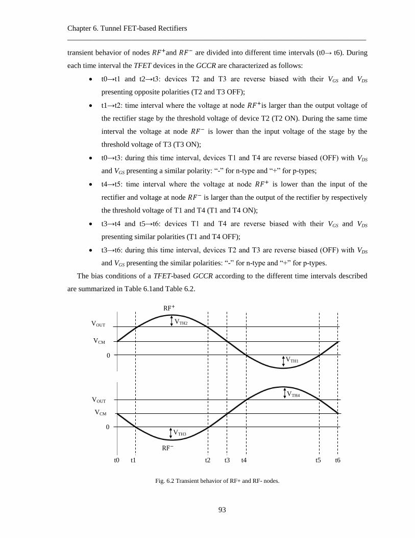
Chapter 6. Tunnel FET-based Rectifiers
________________________________________________________________________________
93
transient behavior of nodes and are divided into different time intervals (t0→ t6). During
each time interval the TFET devices in the GCCR are characterized as follows:
t0→t1 and t2→t3: devices T2 and T3 are reverse biased with their VGS and VDS
presenting opposite polarities (T2 and T3 OFF);
t1→t2: time interval where the voltage at node is larger than the output voltage of
the rectifier stage by the threshold voltage of device T2 (T2 ON). During the same time
interval the voltage at node is lower than the input voltage of the stage by the
threshold voltage of T3 (T3 ON);
t0→t3: during this time interval, devices T1 and T4 are reverse biased (OFF) with VDS
and VGS presenting a similar polarity: “-” for n-type and “+” for p-types;
t4→t5: time interval where the voltage at node is lower than the input of the
rectifier and voltage at node is larger than the output of the rectifier by respectively
the threshold voltage of T1 and T4 (T1 and T4 ON);
t3→t4 and t5→t6: devices T1 and T4 are reverse biased with their VGS and VDS
presenting similar polarities (T1 and T4 OFF);
t3→t6: during this time interval, devices T2 and T3 are reverse biased (OFF) with VDS
and VGS presenting the similar polarities: “-” for n-type and “+” for p-types.
The bias conditions of a TFET-based GCCR according to the different time intervals described
are summarized in Table 6.1and Table 6.2.
Fig. 6.2 Transient behavior of RF+ and RF- nodes.
0
0
VOUT
VOUT
VCM
VCM
t0 t1 t2 t3 t4 t5 t6
RF
RF
VTH2
VTH1
VTH4
VTH3

Chapter 6. Tunnel FET-based Rectifiers
________________________________________________________________________________
94
Table 6.1 Steady-state bias conditions of the TFET-GCCR in region I.
Region I VGS VDS ΔT State
T1 (n) RF RF RF t0 → t3 OFF
T2 (p) RF RF RF
< 0 t1 → t2 ON
> 0 t0 → t1
t2→ t3 OFF, NDR
T3 (n) RF RF RF RF
> 0 t1 → t2 ON
< 0 t0 → t1
t2→ t3 OFF, NDR
T4 (p) RF RF RF t0 → t3 OFF
Table 6.2 Steady-state bias conditions of the TFET-GCCR in region II.
Region II VGS VDS ΔT State
T1 (n) RF RF RF
> 0 t4→ t5 ON
< 0 t3→ t4
t5→ t6 OFF, NDR
T2 (p) RF RF RF t3→ t6 OFF
T3 (n) RF RF RF RF t3→ t6 OFF
T4 (p) RF RF RF
< 0 t4→ t5 ON
> 0 t3→ t4
t5→ t6 OFF, NDR
Similar to the charge-pump topology presented in the previous chapter, the reverse, conduction
and switching power are presented as the main losses in the rectification process. The power
conversion efficiency PCE of the rectifier stage is calculated as shown by equation (6.1).
∫
(6.1)
In Fig. 6.3, the performance comparison of the GCCR designed with heterojunction TFETs
(InAS-GaSb, LG=40 nm) considering two frequencies of operation (100 MHz and 915 MHz) and
loads (RL=100 kΩ and RL=10 kΩ) is presented. TFETs T1 to T4 are simulated with channel widths
of 1 µm. For a frequency of 915 MHz (100 MHz) the coupling capacitors CC present 1 pF (10 pF)
and the load capacitor CL 10pF (100 pF). One can observe that compared to a load of 10 kΩ, a load
of 100 kΩ allows for large PCE values at sub-µW power levels for both frequencies under study.

Chapter 6. Tunnel FET-based Rectifiers
________________________________________________________________________________
95
The peak efficiency for a load of 100 kΩ is shown to be around a RF VAC of 0.2 V. At larger voltage
magnitudes, the decrease of the PCE is not only due to the increase of conduction losses by the
transistors operating in on-state but also due to non-fully closed transistors operating in off-state,
and consequent conduction of reverse current.
Fig. 6.3 Performance comparison of a TFET-based GCCR considering 1 stage.
6.3 Advantages of Tunnel FETs in rectifiers
The improved electrical characteristics of tunneling devices at low-voltage operation in
comparison to conventional thermionic devices allows for increased performance of TFET-based
rectifiers at ultra-low power operation (sub-µW). As will be shown in the following sections, when
compared to thermionic devices the lower reverse current and increased drive current at sub-0.25 V
characterize TFETs in rectifiers with less reverse and conduction losses and consequent larger PCE
at low induced RF voltage. As shown in Table 6.1 and Table 6.2, each TFET device operating in a
GCCR stage presents during most of the period cycle an off-state condition. As an example, the
device T1 is forward biased (on-state) during the time interval t4→t5, while during the remaining
period time, it is reverse biased, i.e. VDS < 0 V. During half of the period cycle (t0→ t3) the
0
20
40
60
80
100
-60 -50 -40 -30 -20 -10
PC
E (%
)
RFIN (dBm)
f=100 MHz TFET GCCR R=100kΩ
TFET GCCR R=10kΩ sub-µW
0
20
40
60
80
100
0 0.2 0.4 0.6 0.8 1
PC
E (%
)
VRF (VAC)
f=100 MHz
TFET GCCR R=100kΩ TFET GCCR R=10kΩ
0
20
40
60
80
100
0 0.2 0.4 0.6 0.8 1
PC
E (%
)
VRF (VAC)
f=915 MHz TFET GCCR R=100kΩ
TFET GCCR R=10kΩ
0
20
40
60
80
100
-60 -50 -40 -30 -20 -10
PC
E (%
)
RFIN (dBm)
f=915 MHz TFET GCCR R=100kΩ
TFET GCCR R=10kΩ
sub-µW

Chapter 6. Tunnel FET-based Rectifiers
________________________________________________________________________________
96
tunneling device T1 is reverse biased with a VGS < 0 V and during the time intervals t3→ t4 and
t5→ t6 it presents a VGS > 0 V. As explained in section 4.2.2, the reverse current of an n-type
tunneling device under this condition (VDS < 0 V and VGS > 0 V) follows a non-monotonic
characteristic, i.e., the magnitude of the reverse current under low reverse bias increases and then
decreases at large reverse bias thus characterizing the TFET with a negative differential resistance
(NDR) region. In Table 6.1 and Table 6.2 one can observe that this condition applies to all the TFET
devices.
In contrast, thermionic devices under such condition present a reverse current that increases in
magnitude with the increase of reverse bias. As shown in Fig. 6.4, the comparison between a
heterojunction n-TFET and thermionic n-FinFET under similar bias conditions (applied during the
time intervals t3→ t4 and t5→ t6) shows that the reverse current of FinFETs is much larger than
that of TFETs. This characteristic leads to large losses (called here as switching losses) in FinFET-
based rectifiers during the mentioned time intervals.
Fig. 6.4 Reverse current of T1 during interval t3→t4, t5→ t6 for: (a) n-type heterojunction TFET and (b) n-type FinFET.
-100
-80
-60
-40
-20
0
-0.05 -0.04 -0.03 -0.02 -0.01 0
Cu
rren
t (µ
A/µ
m)
VDS (V)
Increase RF RF 5 -10
-8
-6
-4
-2
0
-0.05 -0.04 -0.03 -0.02 -0.01 0
Cu
rren
t (µ
A/µ
m)
VDS (V)
VGS=0.1 V
VGS=0.2 V
VGS=0.4 V
VGS=0.3 V
VGS=0.5 V
-500
-400
-300
-200
-100
0
-0.2 -0.15 -0.1 -0.05 0
Cu
rren
t (µ
A/µ
m)
VDS (V)
Increase RF RF 5 -12
-10
-8
-6
-4
-2
0
-0.2 -0.15 -0.1 -0.05 0
Cu
rren
t (µ
A/µ
m)
VDS (V)
VGS=0.1 V
VGS=0.2 V
VGS=0.4 V
VGS=0.3 V
VGS=0.5 V
(a) (bn-HTFET n-FinFET

Chapter 6. Tunnel FET-based Rectifiers
________________________________________________________________________________
97
This condition applies to the four transistors in the GCCR during their respective switching time.
As an example, Fig. 6.5 presents a comparison between the current conducted by the device T1 in
the GCCR stage (considering heterojunction n-TFET and n-FinFET) and the respective power
consumption when considering an input voltage RF VAC of 0.4 V and a load of 100 kΩ
(f=915 MHz). The switching losses of the FinFET counterpart are shown to be much larger at
similar bias conditions, thus resulting in increased losses in FinFET-based rectifiers.
Fig. 6.5 Current and power consumption of transistor T1 in the GCCR during region II of operation. Simulation
conditions: VAC=0.4 V, f=915 MHz, CC=1pF, CL=10 pF, RL=100 kΩ. WT1-HTFET=1µm, NFINS-FinFET=14.
6.4 Drawbacks of Tunnel FETs in rectifiers
As explained in the previous chapter, when the TFET device is subjected to reverse bias
conditions, the intrinsic p-i-n diode of its structure is forward biased. With the increase of reverse
bias occurring at large induced RF voltages (VDS < 0 V in n-TFETs and VDS > 0 in p-TFETs) the
large increase of reverse current in TFETs strongly degrades the performance of TFET-based
rectifiers. As shown in Fig. 6.6, the increase of RF voltage magnitude results in an exponential
increase of the reverse losses (PREV) in the HTFET-GCCR. In contrast, the losses presented by the
FinFET counterpart increase only linearly with RF VAC magnitudes. Therefore, this characteristic
limits the use of TFETs in rectifiers to low voltage operation.
-0.1
0.0
0.1
0.2
0.3
0.4
Vo
ltag
e (V
)
-40
-20
0
20
40
60
80
T1 C
urr
ent
(µA
)
Time (s)
0.0
0.5
1.0
1.5
2.0
T1 P
ow
er (
µw
)
Time (s)
-0.1
0.0
0.1
0.2
0.3
0.4
Vo
ltag
e (V
)
n-HTFET n-FinFET
Sw. losses
Cond. losses
Sw. losses
n-HTFET n-FinFET
VRF- VOUT
VRF+
VRF- VOUT
VRF+

Chapter 6. Tunnel FET-based Rectifiers
________________________________________________________________________________
98
Fig. 6.6 Increase of reverse losses as function of RF VAC magnitude.
6.5 Proposed Tunnel FET-based rectifier
In order to avoid large reverse losses due to large reverse biased TFETs in rectifiers, a possible
solution is to decrease the magnitude of VGS during the off-state condition of the transistor. As
explained in the previous chapter and taking as an example the heterojunction TFET (GaSb-InAs,
LG=40 nm), the reverse current under a VGS=0 V condition is attenuated at a larger reverse bias
range in comparison to a VGS=VDS condition (see Fig. 5.3). Therefore, in order to attenuate the
reverse current of reverse biased TFETs in rectifiers a different topology is required.
In Fig. 6.7, a different rectifier topology for TFET devices is proposed. The rectifier is
characterized by biasing the gate of the main transistors T1 and T3 with when > and
otherwise. In a similar way, the gate of transistors T2 and T4 are biased with when
< and otherwise.
Fig. 6.7 Proposed TFET-based rectifier
0
10
20
30
40
0.1 0.2 0.3 0.4 0.5 0.6 0.7 0.8P
REV
/PIN
(%)
RF VAC
HTFET-GCCR
FinFET-GCCR
f=915 MHz, RL=100 kΩ

Chapter 6. Tunnel FET-based Rectifiers
________________________________________________________________________________
99
In order to accomplish this behavior, transistors T1 and T3 share the same gate, as also T2 and
T4. Two auxiliary TFET devices (T5 and T6) are required to bias the gates of T1 and T3 and two
auxiliary transistors (T7 and T8) to bias the gates of T2 and T4. In the proposed topology, the VDS
bias of the main four transistors (T1-T4) remains the same as the conditions shown in Table 6.1 and
Table 6.2. In contrast, different VGS magnitude is applied to the main transistors.
Fig. 6.8 Active transistors in (a) first and (b) second regions of operation
Fig. 6.9 Ideal transient behavior of proposed TFET-rectifier.
gate_p gate_n
0
0
VOUT
VOUT
VCM
VCM
t0 t1 t2 t3 t4 t5 t6
RF
RF
VTH2
VTH1
VTH4
VTH3
ate_
ate_p

Chapter 6. Tunnel FET-based Rectifiers
________________________________________________________________________________
100
Considering an ideal rectifier (no losses in the transistors), during the first region of operation
shown in Fig. 6.8 (a) ( ) the main transistors T2, T3 and the auxiliary transistors T5 and
T8 are active (T1, T4, T6 and T7 operate in off-state), while the second region of operation shown
in Fig. 6.8 (b) ( ) characterizes T1, T4, T6 and T7 in on-state (T2, T3, T5 and T8 in off-
state). The ideal transient behavior of the proposed rectifier is shown in Fig. 6.9.
According to Table 6.3, when the main transistors are reverse biased (highlighted in bold) the
magnitude of the gate-to-source voltage VGS is ideally zero (considering the ideal transient behavior
shown in Fig. 6.9). As shown in the previous chapter, this condition highly reduces the reverse
current and consequent reverse losses of the topology. In an ideal case, when the main transistors
are forward biased, their VGS magnitude remains the same as the conventional GCCR topology. At
this point, it is important to mention that in the proposed rectifier topology the auxiliary transistors
operating during their off-state condition present a non-zero VGS magnitude and therefore reverse
current in these transistors is expected. In order to mitigate the consequent reverse losses of the
auxiliary transistors and improve the PCE of the rectifier stage one can increase the ratio of widths
between the main and auxiliary devices.
Table 6.3 Ideal VGS conditions of the proposed rectifier in both
regions of operation (bold: transistors in off-state)
VGS Region I t0 → t3 VGS Region II t3 → t6
T1 (n) _ ate_p RF
T2 (p) ate_ RF _
T3 (n) ate_p RF _
T4 (p) _ ate_ RF
6.6 Optimization of proposed rectifier
In this section, the proposed rectifier is simulated for two different frequencies (100 MHz and
915 MHz) considering an output load of 100 kΩ. For a frequency of 915 MHz (100 MHz), coupling
capacitors of 1 pF (10 pF) and load capacitor of 10 pF (100 pF) are considered. For comparison
purposes, the GCCR topology is simulated considering the main transistors T1 to T4 as
heterojunction TFETs (GaSb-InAs, LG=40 nm) with widths of 1 µm. In the proposed rectifier, the
main transistors are simulated as 1 µm and the auxiliary transistors with different widths.
In Fig. 6.10, the performance of the proposed rectifier considering different ratios between the
widths of the main (Wm) and auxiliary (Wa) transistors is presented. One can observe that for both
frequencies of operation and RF magnitudes larger than 0.6 VAC, the proposed rectifier operates with

Chapter 6. Tunnel FET-based Rectifiers
________________________________________________________________________________
101
a larger PCE in comparison to the conventional GCCR (shown in dashed curves). At large voltage,
decreasing the size of the auxiliary transistors is shown to increase the rectification efficiency due to
the reduction of reverse losses suffered by the auxiliary devices when operating in off-state.
Fig. 6.10 Performance of the proposed rectifier considering (a) f=915 MHz and (b) f=100 MHz.
Fig. 6.11 Reverse losses of rectifiers (1 stage) as function of VAC magnitudes considering (a) f=915 MHz (prop. Rect:
Wm/Wa=10) and (b) f=100 MHz (prop. Rect: Wm/Wa=5).
In Fig. 6.11, one can observe that the larger efficiency of the proposed rectifier at RF voltages
above 0.6 VAC is due to the reduction of the reverse losses of the main transistors during their off-
state operation. Despite the increased performance of the proposed TFET rectifier in comparison to
the GCCR counterpart at large voltage, there is a lower efficiency at sub-0.6 VAC.
From the circuit shown in Fig. 6.8, it can be deduced that the large gate-to-drain intrinsic
capacitances (CGD) of the auxiliary transistors operating during on-state are responsible for delays
between the voltage applied in the gate and the source of the main transistors. As shown in Fig. 6.12
(a), this characteristic has implications in the transient behavior of the rectifier stage. When
considering an operation frequency of 915 MHz, the out-of-phase gate and source voltages fail to
provide a VGS close to 0 V when the main transistors are reverse biased. This strongly affects the
0
20
40
60
80
0.0 0.1 0.2 0.3 0.4 0.5 0.6 0.7 0.8
PC
E (%
)
VRF (VAC)
Proposed Rectifier f=100 MHz
Wm/Wa=20Wm/Wa=10Wm/Wa=5Wm/Wa=2
Ratio increasing
GCCR Top. 0
20
40
60
80
0.0 0.1 0.2 0.3 0.4 0.5 0.6 0.7 0.8
PC
E (%
)
VRF (VAC)
Proposed Rectifier f=915 MHz
Wm/Wa=20Wm/Wa=10Wm/Wa=5Wm/Wa=2
Ratio increasing
GCCR top.
(a) (b)
0
10
20
30
40
0.1 0.2 0.3 0.4 0.5 0.6 0.7 0.8
PR
EV/P
IN (
%)
VRF VAC
f=100 MHz, RL=100 kΩ
HTFET-GCCR
FinFET-GCCR
Proposed Rect.
0
10
20
30
40
0.1 0.2 0.3 0.4 0.5 0.6 0.7 0.8
PR
EV/P
IN (
%)
VRF VAC
f=915 MHz, RL=100 kΩ
HTFET-GCCR
FinFET-GCCR
Proposed Rect.
(a) (b)

Chapter 6. Tunnel FET-based Rectifiers
________________________________________________________________________________
102
performance of n-TFETs T1 and T3 under reverse biased conditions by placing them under an NDR
region (VGS >> 0 V and VDS < 0 V) and increased conduction of reverse current (see Fig. 6.4). In
contrast, at a frequency of 100 MHz the reverse biased transistors T1 and T3 are placed in an NDR
region with a small VGS magnitude and consequent low reverse current (VGS > 0 V and VDS < 0 V).
Larger auxiliary transistors can mitigate the delays between the gate and source voltages of the
main transistors at high frequencies by fastening the charge and discharge rate of their parasitic
gate-to-drain capacitances (when forward biased). However, large auxiliary transistors will suffer
from large reverse losses at large RF VAC magnitudes when reverse biased. As shown in Fig. 6.10,
there is a trade-off between the choice of large auxiliary transistors (increase efficiency at sub-0.6
VAC) and small auxiliary transistors (increased efficiency at VAC > 0.6 V). In the following section, a
ratio between the main and auxiliary transistors of 10 and 5 is considered in the proposed rectifier
for respectively f=915 MHz and f=100 MHz.
Fig. 6.12 Gate voltage applied to the main transistors T1 to T4 in the proposed rectifier for: a) f=915MHz (Wm/Wa=10),
b) f=100MHz (Wm/Wa=5).
6.7 Performance comparison of rectifiers
In Fig. 6.13, a performance comparison between a GCCR and the proposed rectifier designed
with heterojunction TFETs (GaSb-InAs, LG=40 nm) is presented. For comparison purposes, the
performance of a FinFET-based GCCR is included (FinFETs with NFINs=14 and LG=20 nm). In both
simulations, 1 rectifier stage is considered.
One can observe that the FinFET-based rectifier produces the lowest power conversion
efficiency at sub -40 dBm when considering the two frequencies of operation under study. It shows,
however, the largest output voltage values for RF VAC magnitudes larger than 0.3 V. This
-0.05
0.00
0.05
0.10
0.15
0.20
0.25
0.30
Vo
ltag
e (V
)
time (s)
f=100MHz, VAC=0.3V, R=100 kΩ
Gate T1, T3
Gate T2, T4
RF RF
-0.05
0.00
0.05
0.10
0.15
0.20
0.25
0.30
Vo
ltag
e (V
)
time (s)
f=915MHz, VAC=0.3V R=100 kΩ
RF
Gate T1, T3
Gate T2, T4
RF
(a) (b)
Large reverse
current
Small reverse
current

Chapter 6. Tunnel FET-based Rectifiers
________________________________________________________________________________
103
characteristic is explained due to the larger current conducted by FinFETs above 0.25 V when
compared to heterojunction TFETs.
At sub -25 dBm and f=915 MHz, the conventional HTFET-GCCR is shown to produce the
largest power efficiencies. At the same frequency, the proposed HTFET-rectifier shows a degraded
efficiency at RF power levels between -25 dBm and -40 dBm (corresponding to RF VAC between
0.2 V and 0.6 V) due to the increased losses of the main transistors (n-TFETs placed in an NDR
region). At sub -40 dBm the performance of both HTFET-based rectifiers is similar (reverse current
of n-TFETs in the proposed rectifier is negligible).
Fig. 6.13 Performance comparison of rectifiers for two frequencies of operation.
0.0
0.2
0.4
0.6
0.8
0.0 0.2 0.4 0.6 0.8
VO
UT
(V)
VRF (VAC)
f=915 MHz, R=100kΩ TFET GCCRProp. RectifierFinFET GCCR
0.0
0.2
0.4
0.6
0.8
0.0 0.2 0.4 0.6 0.8
VO
UT
(V)
VRF (VAC)
f=100 MHz, R=100kΩ TFET GCCR
Proposed Rectifier
FinFET GCCR
0
20
40
60
80
100
-60 -50 -40 -30 -20 -10
PC
E (%
)
RFIN (dBm)
f=100 MHz, R=100kΩ TFET GCCRProposed Rect.FinFET GCCR
0
20
40
60
80
100
0 0.2 0.4 0.6 0.8 1
PC
E (%
)
VRF (VAC)
f=100 MHz, R=100kΩ
TFET GCCR
Proposed Rect.FinFET GCCR
0
20
40
60
80
100
0 0.2 0.4 0.6 0.8 1
PC
E (%
)
VRF (VAC)
f=915 MHz, R=100kΩ TFET GCCRProp. RectifierFinFET GCCR
0
20
40
60
80
100
-60 -50 -40 -30 -20 -10
PC
E (%
)
RFIN (dBm)
f=915 MHz, R=100kΩ TFET GCCRProp. RectifierFinFET GCCR

Chapter 6. Tunnel FET-based Rectifiers
________________________________________________________________________________
104
At a frequency of 100 MHz and sub -25 dBm, the proposed HTFET-rectifier and HTFET-GCCR
present a similar performance. The proposed HTFET-rectifier shows, however, improved power
efficiencies when compared to the counterpart rectifiers at RF power levels above -25 dBm. This is
due to the reduction of reverse losses in the main transistors when the proposed-HTFET rectifier is
subjected to RF VAC magnitudes larger than 0.6 V. This characteristic is observed for the two
frequencies of operation under study.
According to the results, there is suitable rectifier topology for different regions of voltage
operation and low/high frequencies. In Table 6.4, a summary of suitable rectifier topologies is
presented for different operation conditions.
Table 6.4 Suitable rectifier topology for different voltage/power range.
Ultra-low Voltage Low-Voltage Medium Voltage
Voltage Range < 200 mV 200-600 mV > 600 mV
frequency 100 MHz 915 MHz 100 MHz 915 MHz 100 MHz 915 MHz
Suitable
Topology
HTFET-GCCR
Prop. Rect. HTFET-GCCR Prop. Rect. HTFET-GCCR Prop. Rect. Prop. Rect.
6.8 Chapter summary
In this chapter, a performance comparison between rectifiers designed with tunneling and
thermionic-based devices is presented. It is shown that when the heterojunction TFET is reverse
biased, the consequent conduction of reverse current at large induced RF voltage strongly degrades
the performance of the rectifier stage. Therefore, a different rectifier topology is proposed: when the
tunnel devices are reverse biased, a VGS=0 V is applied to their terminals in order to reduce the
conduction of reverse current and increase the rectifier stage efficiency. In order to accomplish this
characteristic, an auxiliary rectifier inside the rectifier stage is proposed. In order to reduce the
losses of the auxiliary circuit, the ratio between the widths of the main and auxiliary transistors can
be increased. When compared to the conventional gate cross-coupled topology, the proposed TFET-
based rectifier is shown to produce the largest rectification efficiencies at a wider range of
voltage/power operation under an operating frequency of 100 MHz.
To conclude, the inclusion of heterojunction TFETs in rectifiers can improve the field of RF
energy harvesting by allowing larger power conversion efficiencies at power/voltage levels where
conventional thermionic devices are shown to be inefficient.

Chapter 6. Tunnel FET-based Rectifiers
________________________________________________________________________________
105
6.9 References
1 Paing T. et al., ‘‘Custom IC for ultralow power RF energy scavenging,’’ IEEE Trans. Power
Electron., vol. 26, no. 6, pp. 1620–1626, Jun. 2011.
2 Adami S-E. et al., "Ultra-low Power Autonomous Power Management System with Effective
Impedance Matching for RF Energy Harvesting," in Int.Power Syst. (CIPS), Int. Conf. on ,
pp.1-6, Feb. 2014.
3 Sain G. et al., "A battery-less power management circuit for RF energy harvesting with input
voltage regulation and synchronous rectification," in Circ, and Syst., Int. Mid. Symp. on, pp.1-
4, Aug. 2015.
4 Jinpeng, S. et al. “Design and implementation of an ultra-low power passive UHF RFID tag”,
J. Semiconductors, vol. 33, no. 11, pp.115011, Nov. , 2012.
5 Liu D.-S. et al. “New Analysis and Design of a RF Rectifier for RFID and Implantable
Devices,” Sensors, vol.11, no.7, pp.6494-6508, 2011.
6 Jinpeg S. et al. “A passive RFID tag with a dynamic-VTH-cancellation rectifier,” J.
Semiconductors, vol.34, no.9, p.95005, Sep. 2013.
7 Burasa P., Constantin N. G. and K. Wu, "High-Efficiency Wideband Rectifier for Single-Chip
Batteryless Active Millimeter-Wave Identification (MMID) Tag in 65-nm Bulk CMOS
Technology," Microwave Theory and Techniques, IEEE Trans. on , vol.62, no.4,
pp.1005,1011, April 2014.
8 Mandal, S. and Sarpeshkar, R “Low-Power CMOS Rectifier Design for RFID Applications”,
Circuits Syst., IEEE Trans. vol.54, no.6, pp.1177-1188, 2007.
9 Liu H. et al., “Tunnel FET RF Rectifier Design for Energy Harvesting Applications,”
Emerging and Selected Topics in Circuits and Systems, IEEE Journal on, vol.4, no.4, pp.400-
411, Dec. 2014.


107
Chapter 7
7. TFET-based Power Management Circuit for RF
Energy Harvesting
In this chapter, a Tunnel FET (TFET)-based Power Management Circuit (PMC) for ultra-low
power RF energy harvesting applications is proposed. Advantages of using tunneling devices in RF
PMC are identified, as also the challenges on the design of inductor-based boost converters due to
the different electrical characteristics of TFETs under reverse bias conditions. The proposed TFET-
PMC shows promising results at available RF power levels below -20 dBm (f=915 MHz). For an
available power of -25 dBm, the proposed converter is able to deliver 1.1 µW of average power to a
load (0.5 V) with a boost efficiency of 86 %.
In order to allow maximum power transfer between the front-end rectifier and the boost
converter, the TFET-PMC adapts its input impedance. Once the output of the boost converter
reaches 0.5 V, a load is enabled and the PMC starts a self-sustaining mode of operation. All the
simulated results are based on the Verilog-A based LUT TFET models and PTM-based FinFET
models described in Chapter 4
7.1 Motivation
With the fast progression in the development of low power embedded systems, the design of
efficient circuits at reduced voltage operation has gained momentum in recent years [1-2]. Low
voltage and power systems, like biomedical implants or wearable devices are examples of
applications that can benefit from harvesting surrounding electromagnetic radiation, thus reducing

Chapter 7. TFET-based Power Management Circuit for RF Energy Harvesting
________________________________________________________________________________
108
battery size and extending its lifetime. Several works have already demonstrated wireless powering
of a load at short distances with UHF radiation at legally transmitted power levels [3-11].
However, the received radiation power attenuates with distance, and low power conversion
efficiency (PCE) demonstrated by front-end rectifiers at low RF power levels (sub -20 dBm)
constrains the operation distance of RF energy harvesters to short distances.
Low power levels of electromagnetic radiation produce low output voltage values in the
receiving antenna and therefore, efficient rectifiers are required for a proper system operation. In
Chapter 6, it was shown by simulations that TFET-based rectifiers can outperform thermionic-
device based counterparts under extreme low-voltage/power scenarios (sub -20 dBm). In addition
and as shown in section 4.3, the particular electrical characteristics of tunneling devices enable the
decrease of energy per switch operation, thus allowing the design of efficient digital cells at low
voltage in comparison to conventional CMOS [12-14]. This characteristic can enable the design of
efficient PMC at low voltage operation (sub-0.25 V). Therefore, it is of interest to explore the
performance and limitations of tunneling devices in ultra-low voltage PMCs for RF energy
harvesting applications.
7.2 Challenges in RF power transport
In Fig. 7.1, the structure of the RF power transport system considered in this work is presented.
The receiver comprises a receiving antenna with 50 Ω standard impedance followed by a lumped
matching network between the antenna and the rectifier. The power management circuit (PMC) is
required to boost the rectifier output voltage to a larger and stable voltage in order to power a
load/sensor.
Fig. 7.1 RF Power Transport System.
The main challenge in the receiver of the RF power system is to overcome the power-density
attenuation due to long distances between the transmitter and receiver circuits. The Friis equation
expressed by equation (7.1) indicates that the power received at the input of the rectifier PR is
dependent on the transmitted power PT, transmitter and receiver antenna gains GT and GR

Chapter 7. TFET-based Power Management Circuit for RF Energy Harvesting
________________________________________________________________________________
109
respectively, wavelength of the transmitter signal and propagation distance R [1]. If the receiver
antenna is well matched with the rectifier, the relation between the peak amplitude of the antenna
VA and the received power can be expressed by equation (7.2), with RA representing the real part of
the antenna impedance.
(
)
(7.1)
√8 (7.2)
In Table 7.1, the license-free Industry-Science-Medical (ISM) frequency bands for different
regions are indicated [2]. Considering two different frequency bands (915 MHz and 2.4 GHz), a
maximum regulated transmitter power of 4 W and taking into account equations (7.1) and (7.2), one
can calculate the received power and the peak amplitude of the antenna as a function of the
propagation distance R as shown in Fig. 7.2 (assuming antenna gains of 1). It is shown that the
power density attenuation at the input of the rectifier as a function of the propagation distance
constrains the operation of RF systems to short distances.
Table 7.1 Frequency Band allocations and maximum transmitter power [1].
Freq. Band (MHz) Transmitter Power Region
2446-2454 500 mW-4 W (EIRP) Europe
867.6-868 500 mW (ERP) Europe
902-928 4 W (EIRP) USA/Canada
2400-2483.5 4 W (EIRP) USA/Canada
2400-2483.5 10 mW (EIRP) Japan/Korea
Fig. 7.2 (a) Received power and (b) peak amplitude of the antenna as a function of propagation distance for PT = 4 W.
0.00
0.01
0.10
1.00
10.00
0 5 10 15 20 25 30 35 40 45 50Peak
Am
pl.
An
ten
na
(V)
Propagation Distance (m)
915 MHz2400 MHz
PT=4W
Prop. Distance with low rect. efficiency
-40-35-30-25-20-15-10
-50
0 5 10 15 20 25 30 35 40 45 50
Rec
eive
d P
ow
er (
dB
m)
Propagation Distance (m)
915 MHz
2400 MHzPT=4W
Limited Efficiency below -25 dBm
(a) (b)

Chapter 7. TFET-based Power Management Circuit for RF Energy Harvesting
________________________________________________________________________________
110
Fig. 7.3 Comparison of (a) CMOS rectifiers from literature and (b) rectifier output voltage as function of available power.
As an example and according to Fig. 7.2 (a) the receiving antenna is sensing -25 dBm at a
propagation distance of 30 m from the transmitter (f=915 MHz, PT=4 W). As shown in Fig. 7.2 (b),
at 30 m the receiving antenna produces a peak voltage amplitude of 36 mV. At such low voltage
levels, there is a clear difficulty of rectification as shown by the recent results from the state of the
art CMOS rectifiers shown in Fig. 7.3.
In order to increase the input voltage of the rectifier and consequent PCE of rectification, a
resonating LC network optimized for a desired input power level can be included at the output of
the antenna as shown in Fig. 7.4 (a) [1, 6]. This method is adopted in the proposed RF PMC. In the
front-end part of the RF PMC, the gate cross-coupled rectifier (GCCR) topology shown in
Fig. 7.4 (b) is considered and matched with a 50 Ω antenna.
Fig. 7.4 (a) Equivalent circuit of antenna-matching-rectifier and (b) TFET-based GCCR topology.
0
20
40
60
80
-35 -30 -25 -20 -15 -10 -5 0
RF-
DC
Eff
icie
ncy
(%
)
Pav (dBm)
Limited Efficiency at low RF signals
This work
[7] [11]
[3]
[9]
[4][8]
[10][6]
[5]
0
0.5
1
1.5
2
2.5
3
-30 -25 -20 -15 -10 -5 0
Rec
t. V
OU
T (V
)
Pav (dBm)
This work
[11]
[8]
[6] [9]
[7]
[3]
[4] [10]
[5]
(b) (a)
Receiving
Antenna
LC Matching
Network
Equivalent
Rectifier
(a) (b)

Chapter 7. TFET-based Power Management Circuit for RF Energy Harvesting
________________________________________________________________________________
111
Fig. 7.5 (a) Rectifier efficiency as function of available power considering different technologies; (b) Heterojunction
TFET-based rectifier PCE as a function of output load; (c) Rectifier output power as a function of output voltage for
heterojunction TFET-based rectifier.
In Fig. 7.5 (a), the PCE of a GCCR with one-stage designed with different technologies is
presented. For the rectifier design, heterojunction TFETs (InAs-GaSb, LG=40 nm), homojunction
TFETs (InAs, LG=20 nm) and Si-FinFETs (LG=20 nm) are considered. Each transistor is simulated
with a channel width of 10 µm. The matching network with L and C elements is optimized for each
rectifier considering an available power of -20 dBm.
The results show that the heterojunction TFET-based rectifier presents higher rectification
efficiencies in the range of -30 to -25 dBm when compared to the FinFET-based rectifier. At such
low power levels the homojunction TFET-based GCCR presents the lowest efficiency values.
Compared to the FinFET-based rectifier, the higher efficiency shown by the heterojunction TFET-
based counterpart is explained due to the better switching performance of individual TFET
transistors at sub-0.2 V operation (see Chapter 6).
With a focus on the heterojunction TFET-based rectifier, Fig. 7.5 (b) shows that at different
power levels, the range of optimum load impedance for maximum efficiency changes. One can
observe that increasing the available power results in lower optimum load impedance values for
maximum efficiency. As shown in Fig. 7.5 (c), this behavior results in increased optimum rectifier
output voltage at large available RF power. For a good RF PMC design, knowing in advance the
0.01
0.10
1.00
10.00
100.00
0 100 200 300 400 500
PO
UT
(µW
)
VOUT (mV)
Pav=-20 dBm
Pav=-25 dBm
Pav=-30 dBm
Max. PCE
142mV
61mV
217mV
0
20
40
60
80
100
1E+03 1E+04 1E+05 1E+06
PC
E (%
)
RL (Ω)
Pav=-20 dBmPav=-25 dBmPav=-30 dBm
Pav. Increasing
0
20
40
60
80
100
-30 -25 -20
PC
E (%
)
Pav (dBm)
Het. TFET-Rectifier
Si. Rectifier
Homo. TFET-Rectifier
(a)
(b)
(c)

Chapter 7. TFET-based Power Management Circuit for RF Energy Harvesting
________________________________________________________________________________
112
load range that maximizes the rectifier efficiency is mandatory in order to allow maximum power
transfer from the rectifier to the input of the boost converter.
7.3 Proposed TFET-based PMC
In Fig. 7.6, the building blocks of the proposed RF TFET-based PMC are presented. The RF
power source is simulated as a port with 915 MHz and 50 Ω impedance. After matching and
rectification the PMC is required to boost the low output voltage of the rectifier to 0.5 V and then
enable a load. The PMC is divided in three distinct modules: startup, controller and boost circuit.
The first module is responsible for pre-charge the power capacitors connected to nodes VDDINT
and VDDSTARTUP (by the rectifier) and the input CBOOST and output COUT capacitors of the boost
converter circuit to adequate voltage values before enabling the boost converter operation.
Fig. 7.6 Proposed RF TFET-based Power Management Circuit for energy harvesting applications.

Chapter 7. TFET-based Power Management Circuit for RF Energy Harvesting
________________________________________________________________________________
113
The controller circuit (powered by the capacitors of the startup module) is responsible for
providing control signals to the switches of the boost converter circuit. When the boost converter
operation takes place and the load is enabled for the first time, the PMC enters into a self-sustaining
mode (SSM) of operation, i.e. the power capacitors are directly charged by the output capacitor COUT
and not by the rectifier. In order to increase the PMC efficiency, the controller module is
responsible for imposing an adequate voltage to the input of the boost converter (that interfaces
with the output of the rectifier) in order to maximize the rectifier efficiency.
7.3.1 Startup Circuit
The proposed startup module is designed with the purpose of avoiding the use of any external
power source for a proper PMC operation. As shown in Fig. 7.6 a ring oscillator powered by the
rectifier is required for generating two non-overlapped clock signals that are applied to a multi-stage
gate cross-coupled charge pump (GCCCP). In Chapter 5 it was shown by simulations that a TFET-
based GCCCP (designed with heterojunction TFETs) can double the input voltage with magnitudes
as low as 80 mV. In this work, the charge pump is required to charge the capacitor connected at
node VDDSTARTUP in order to power all the analog and digital circuitry of the startup module.
Fig. 7.7 Digital and analog circuitry of the startup module.

Chapter 7. TFET-based Power Management Circuit for RF Energy Harvesting
________________________________________________________________________________
114
Fig. 7.8 (a) Voltage reference and (b) comparator circuit topologies applied in the voltage monitor block of startup circuit.
As shown in Fig. 7.7, a voltage monitor is required to trigger a signal Setboost each time the
node VDDSTARTUP reaches 200 mV. This signal is required to enable the boost conversion. A voltage
reference circuit such as the one shown in Fig. 7.8 (a) provides a fixed 50 mV reference to the
comparator of the voltage monitor block. In [15] the authors have shown that this voltage reference
topology designed with TFETs presents a low dependence on power supply voltage and
temperature. The comparator of the voltage monitor is based on the hysteresis comparator shown in
Fig. 7.8 (b). The 50 mV of the voltage reference circuit is applied to the negative input of the
comparator (M2) and also required to bias the differential pair (through M5).
Before enabling the boost conversion, the input CBOOST and output COUT capacitors of the boost
converter are pre-charged to 200 mV (from node VDDSTARTUP) by the TFET switches controlled by
T3 and T4. Once charged, a signal set_vin_vout is enabled and the boost operation starts. The TFET
switch controlled by T1 is required to allow the charging of the capacitor connected to the input of
the boost converter. The output of the rectifier is responsible for this charging each time the signal
Setboost is active. The TFET switch controlled by T5 is required to allow the charging of the
capacitor at node VDDINT to the same voltage level of node VDDSTARTUP, i.e. 200 mV and the switch
controlled by T7 to enable this capacitor as the power source of the digital and analog circuitry in
the controller module.
Once the output load of the system is enabled, i.e. node VLOAD goes from low-to-high state, a
signal SSM (Self-Sustaining Mode) is triggered and the TFET switch controlled by T2 deactivates
the ring oscillator, clock signals and the charge pump circuit. Then, the output capacitor COUT is
responsible for charging the capacitor connected to the node VDDSTARTUP through the TFET switch
(a) (b)
𝑉𝑅𝐸𝐹 (𝑅
𝑅 ) |𝑉𝐺𝑆 𝑀7|
|𝑉𝐺𝑆 𝑀5|

Chapter 7. TFET-based Power Management Circuit for RF Energy Harvesting
________________________________________________________________________________
115
controlled by T6. In the digital circuitry of the startup module, the signal outcomp3 (coming from
the controller module) is responsible for triggering the SSM signal. Inside the startup module, two
level shifter circuits are required to match the voltage of both the input and power source of digital
cells. The relevance of level shifters in TFET-based circuits is explained in section 7.3.3.
7.3.2 Boost Circuit
In order to increase the output voltage of the rectifier to voltage values suitable to be applied to
the output load, a boost converter is required. In Fig. 7.9 an inductor-based boost converter
topology for TFET devices is proposed. The sequence of operation for the gate controls of each
TFET device is shown in Fig. 7.10.
After a proper startup operation and Setboost signal enabled, the input capacitor CBOOST is
charged and discharged maintaining an average voltage (matching voltage) adequate for maximum
rectifier efficiency. This matching technique is used by several works [16-18], allowing for
maximum transfer of power from the rectifier to the boost converter.
The suitable matching voltage depends on the received power. According to the rectifier output
power as a function of output voltage shown in Fig. 7.5 (c), the optimum reference voltage at the
input of the boost converter (output of rectifier) for maximum power efficiency is 142 mV if an
available power of -25 dBm is considered. If the available RF power changes, the reference voltage
value at the input of the boost converter has to change accordingly. In order to perform a rectifier-
boost matching, the PMC charges and discharges CBOOST, maintaining an average voltage close to
142 mV (VIN between VREF and VMIN as shown in Fig. 7.10).
During the time interval t0 to t1 the input capacitor CBOOST is charged by the rectifier up to VREF.
During this time interval, no current should flow through the inductor. In order to accomplish this,
the TFET device S1 in Fig. 7.9 is closed and a small current flows through the inductor.
Fig. 7.9 Proposed boost converter topology for TFET devices.

Chapter 7. TFET-based Power Management Circuit for RF Energy Harvesting
________________________________________________________________________________
116
Fig. 7.10 Transient behavior of the main electrical signals when the boost controller is enabled.
The absence of body diode in reverse biased TFETs (due to a different doping structure than that
of thermionic MOSFETs) requires a change in the conventional boost converter topology. During
the reverse bias time interval of the output transistor S4 (t0 to t1) a snubber circuit (designed with
TFET device S3 and a capacitor CSNUB) provides a path for the inductor current to flow. During the
time interval t1 to t2, the TFET device S2 is closed in order to charge the inductor from the input
capacitor, until the latter is discharged to a minimum reference value VMIN. During this time interval
the remaining transistors are open. During the time interval t2 to t3, the TFET S4 is closed in order
to allow the transfer of stored energy in the inductor to the output capacitor COUT thus increasing the
output voltage of the boost converter. When the output of the boost converter achieves a reference
value of 510 mV the TFET device S5 is closed and an external load is enabled until the output
capacitor is discharged to 490 mV.
VREF
VMIN
Time (s)
t2 t3 t0 t1
VIN
VCTRN
IL
VCTRP
Vx
VCTR SNUB
VCTR IND
VOUT

Chapter 7. TFET-based Power Management Circuit for RF Energy Harvesting
________________________________________________________________________________
117
7.3.2.1 Challenges in TFET-based boost converter design
In order to increase the conversion efficiency of inductor-based boost converters with TFETs, it
is mandatory to keep a low reverse current conduction from the output transistor S4 during the time
interval t0 to t2, i.e. when the device is reverse biased (VDS > 0 V), see Fig. 7.11 (a). In the previous
chapters, it was shown that reducing the gate bias magnitude of reverse biased TFETs allows for the
reduction of reverse current at low reverse drain bias. However, at large reverse drain bias the
reverse current of TFETs follows the behavior of a diode. This characteristic is shown in Fig. 7.11
(b), i.e. the increase of drain to source voltage magnitude in the p-TFET device S4 results in
increased reverse current and a consequent increase of discharge rate in the output capacitor. The
reverse current is simulated for three technologies (homojunction and heterojunction TFETs and Si-
FinFET) as a function of VDS (> 0 V, p-device S4 reverse biased). The results consider TFETs with
a VGS magnitude equal to 0 V, while a gate voltage equal to VOUT is considered for the reverse biased
FinFET.
During the time interval t0 to t1, the source node of the output transistor S4 equals VIN (assuming
that no current is flowing through the inductor) and therefore VDS of S4 equals VOUT-VIN. As an
example, if the input voltage of the boost converter is 0.1 V and the required output voltage is 0.8 V
(VDS=0.7 V), then during this time interval the reverse current conducted by the GaSb-InAs TFET
device S4 is approximately 2 orders of magnitude larger than that of the FinFET device S4 for a
similar channel width. Since the time interval t0 to t1 dominates the period of the boost operation,
an increase of boost frequency can reduce the discharge rate of the output capacitor COUT.
During the time interval t1 to t2, the source node of the output transistor S4 is at 0 V and its VDS
equals VOUT. Considering the previous example, if one requires an output voltage of 0.8 V then the
reverse current conducted by the heterojunction TFET device S4 is more than 2 orders of magnitude
larger than that of the FinFET device S4 when considering a similar channel width. During this
time interval, an inductor current larger than the reverse current of S4 is required in order to allow
the storage of energy in the inductor. In order to reduce the discharge rate of COUT and consequently
improve the boost efficiency, several solutions can be adopted: decrease the boost frequency
(requires larger inductor current), decrease the size of S4 or increase the size of the output capacitor.
During the time interval t2 to t3, S4 is forward biased conducting current from the inductor to
the output capacitor and therefore, a large output transistor channel width is preferable in order to
attenuate the conduction losses. Therefore, there is a trade-off between choosing a large transistor
S4 to reduce forward conduction losses or a small transistor channel to attenuate the reverse current.

Chapter 7. TFET-based Power Management Circuit for RF Energy Harvesting
________________________________________________________________________________
118
Fig. 7.11 (a) Top: CBOOST charging from rectifier; Middle: Inductor charging from CBOOST; Bottom: Inductor discharging
to COUT; (b) Reverse current for different technologies as a function of VDS in S4.
7.3.2.2 Advantages of TFETs in PMC and boost converters
The analysis of the internal resistance of a transistor as a function of |VDS| is useful to evaluate
the performance of the device in a PMC and boost converter. As shown in Fig. 7.12, the
heterojunction TFET device presents the lowest internal resistance under forward bias conditions at
sub-0.25 V. When compared to conventional MOSFETs, this characteristic allows for decreased
conduction losses in the input transistor S2 during the time interval t1 to t2, and decreased
conduction losses in the output transistor T4 during the charge time of the output capacitor (time
interval t2 to t3). Furthermore, the lower static and dynamic power consumption of TFET-based
circuits at 0.2 V allows for a minimization of energy required for a proper boost controller operation
when compared to the use of conventional thermionic technologies. The larger current conducted by
TFETs at sub-0.2 V operation also enable the design of buffers (applied to the transistors of the
boost converter) with smaller dimensions.
In comparison to Si-FinFETs and under a specific reverse bias conditions range, the larger
internal resistance of Tunnel FETs (ROFF) allows for reduced reverse losses in boost converters. As
shown in the previous section, this characteristic is presented as an advantage if the output transistor
of the boost converter (S4) presents a low reverse bias magnitude, e.g. |VDS| < 0.3 V for
homojunction TFET and |VDS|< 0.6 V for heterojunction TFET. At larger reverse bias magnitudes,
the reverse current conducted by TFETs (larger than Si-FinFETs) increases the reverse losses of the
(b) (a)
1E-16
1E-14
1E-12
1E-10
1E-08
1E-06
1E-04
1E-02
0.0 0.1 0.2 0.3 0.4 0.5 0.6 0.7 0.8
|Ire
v| (
A/µ
m)
VOUT -Vx (V)
GaSb-InAs TFETInAs TFETSi-FinFET

Chapter 7. TFET-based Power Management Circuit for RF Energy Harvesting
________________________________________________________________________________
119
boost converter, constraining the operation of TFET-based boost converters to low voltage
operation.
Fig. 7.12 Internal resistance of different technologies (n-type) under reverse (VDS < 0V) and forward (VDS > 0V) bias.
FinFETs under reverse bias present VGS=VDS, whereas for TFET VGS=0V.
7.3.3 Controller Circuit
For a proper boost converter operation, a controller is required. In Fig. 7.13, a TFET-based
controller is proposed. In order to reduce the reverse losses of the TFETs and improve the controller
efficiency, the circuit imposes a VGS=0 V to all the TFET devices under reverse bias state. The
differential pairs of the two-stage comparators are biased with 50 mV (see Fig. 7.8 b) coming from
the voltage reference of the startup circuit.
The first comparator is required to trigger the Vctrn signal (applied to S2), maintaining the
voltage of the input capacitor CBOOST between a minimum (VMIN) and a reference voltage (VREF). The
second comparator is required to detect a change of polarity in the inductor current, triggering a
Reset signal that is applied to an RS latch. Depending on the state of Vctrn the output transistor S4
is conducting or blocking current according to the signal Vctrp. The third comparator is required to
enable/disable the output load RL by controlling the TFET device S5. The load is enabled when the
output voltage VOUT is between the range of 490 mV and 510 mV. To maximize the controller
efficiency, the second and third comparators (comp2 and comp3) only operate during the fraction of
time when both Vctrn and Vctrp signals are at 0 V. This condition triggers the signal setcomp that
enable the differential pair of the comparator as shown in Fig. 7.8 (b). The first comparator is
enabled as long as the signal Setboost is active.
In order to reduce the current through the inductor during the time interval t0 to t1 the control
signal Vctrind is triggered from an RS latch when both the input S2 and output S4 transistors are
1E+02
1E+03
1E+04
1E+05
1E+06
1E+07
1E+08
1E+09
1E+10
1E+11
0 0.2 0.4 0.6 0.8
Inte
rnal
Res
ista
nce
(Ω
)
|VDS| (V)
Si. FinFET
VGS [0.1V-0.8V]
ROFF
RON
1E+02
1E+03
1E+04
1E+05
1E+06
1E+07
1E+08
1E+09
1E+10
1E+11
0 0.2 0.4 0.6 0.8In
tern
al R
esis
tan
ce (
Ω)
|VDS| (V)
HOMO. TFET
VGS [0.1V-0.8V]
ROFF
RON
1E+02
1E+03
1E+04
1E+05
1E+06
1E+07
1E+08
1E+09
1E+10
1E+11
0 0.2 0.4 0.6 0.8
Inte
rnal
Res
ista
nce
(Ω
)
|VDS| (V)
ROFF under reverse bias
RON under forward bias
HET. TFET
VGS [0.1V-0.8V]

Chapter 7. TFET-based Power Management Circuit for RF Energy Harvesting
________________________________________________________________________________
120
operating during their off-state. The Vctrp and Vctrsnub signals are generated by buffers powered
by Vx_aux. Since the node Vx of Fig. 7.11 (b) is grounded during the operation time interval t1 to
t2, the mentioned buffers cannot be powered directly by Vx. In Fig. 7.14 (a), the proposed circuit
guarantees that during the time interval t1 to t2, the voltage node Vx_aux equals the voltage node
Vin (M1 is open and M2 closed). During the time interval t2 to t3, the node Vx is at a higher voltage
than that of the node Vin and therefore Vx_aux equals Vx (M1 is closed and M2 is open).
Fig. 7.13 Proposed TFET-based controller circuit applied to the boost converter.
Fig. 7.14 (a) Vx_aux generator circuit and (b) Level shifter (LS) circuit block.
(a) (b)

Chapter 7. TFET-based Power Management Circuit for RF Energy Harvesting
________________________________________________________________________________
121
TFET-based digital cells are very sensitive to mismatches between digital levels and power
supply. In order to improve the controller efficiency, level shifter (LS) blocks are required to match
the voltage at the input of the various digital cells with the applied power supply voltages. In
Fig. 7.14 (b) the topology of the TFET-based LS is presented. A detailed study on TFET-based LS
and the power consumption associated with the voltage conversion can be found in [19].
Fig. 7.15 shows the increase of current consumption in several digital cells used in the proposed
PMC as a function of ratio between the input voltage of the cell and a power supply voltage of
0.2 V. In the y axis, the current gain is calculated as IMATCHED*/IMATCHED where IMATCHED is the
nominal current consumption of the cell when the magnitude of the input voltage of the cell equals
the power supply voltage (0.2 V) and IMATCHED* is the current consumption of the cell when the
input voltage of the cell is lower than that of the power supply voltage. In Fig. 7.16, the increase of
current consumption is shown for inverter cells.
Fig. 7.15 Increase of current consumption in digital cells for non-matched input (VIN) and power supply voltage
(VDD=0.2 V).
Fig. 7.16 Increase of current consumption in inverter cells for non-matched input (VIN) and power supply voltage.
1E+0
1E+1
1E+2
1E+3
1E+4
1E+5
0.6 0.7 0.8 0.9 1
Cu
rrre
nt
Gai
n
VIN/VDD
ANDNANDORNORXOR
Het. TFET 1E+0
1E+1
1E+2
1E+3
0.6 0.7 0.8 0.9 1
Cu
rren
t G
ain
VIN/VDD
ANDNANDORNORXOR
Homo. TFET 0
2
4
6
8
10
0.6 0.7 0.8 0.9 1
Cu
rren
t G
ain
VIN/VDD
ANDNANDORNORXOR
FinFET
1E+0
1E+1
1E+2
1E+3
1E+4
1E+5
1E+6
0.6 0.7 0.8 0.9 1
Cu
rren
t G
ain
VIN/VDD
VDD=0.2VDD=0.3VDD=0.4VDD=0.5
Het. TFET
1E+0
1E+1
1E+2
1E+3
1E+4
0.6 0.7 0.8 0.9 1
Cu
rren
t G
ain
VIN/VDD
VDD=0.2VDD=0.3VDD=0.4VDD=0.5
Homo. TFET
0
20
40
60
80
100
120
140
160
0.6 0.7 0.8 0.9 1
Cu
rren
t G
ain
VIN/VDD
VDD=0.2
VDD=0.3
VDD=0.4
VDD=0.5
FinFET

Chapter 7. TFET-based Power Management Circuit for RF Energy Harvesting
________________________________________________________________________________
122
From both simulations one can observe that the current consumption (and consequent power
consumption) of TFET-based digital cells is much more sensitive to mismatches between input and
power supply voltages than that of thermionic-based digital cells. This behavior is directly related to
the exponential increase of current in TFETs (at low voltage) due to the different carrier injection
mechanism. Therefore, in order to avoid an exponential increase of power consumption in TFET-
based cells due to voltage mismatches and consequent degradation of power efficiency in the
proposed PMC, the use of LS is mandatory.
7.4 Simulation Results
This section presents simulation results that explore the performance of the proposed PMC
designed with heterojunction III-V TFETs (InAs-GaSb, LG=40 nm) based on the Verilog-A LUT
models described in Chapter 4. In Fig. 7.17, the transient behavior of the circuit is presented for an
available RF power of -25 dBm. It is shown that prior to the boost conversion operation, the input
CBOOST and output COUT capacitors are pre-charged to 200 mV. Once charged, the power supply
node of the controller is enabled (VDD) and the boost converter starts a synchronous mode of
operation.
One can observe that once the load is enabled, the circuit enters in a self-sustaining mode (SSM)
of operation, i.e. the output capacitor is responsible for charging the capacitors required to power
the startup module and the controller (CVDDINT and CVDDSTARTUP). With SSM active, the ring oscillator
and charge-pump are deactivated, and the charge rate of the capacitors presented in the startup
module is faster, thus reducing the off-time of the boost conversion (Setboost signal off).
The voltage at the input node of the boost converter (VIN) is regulated with an average voltage of
approximately 142 mV, thus allowing maximum transfer of power from the rectifier (1.28 µW)
according to Fig. 7.5 (c). During the time interval t1 to t2, VIN and the inductor current are related to
the inductor L and input capacitor CBOOST as follows [18]:
c s (
√ ) (7.3)
√
si (
√ ) (7.4)
According to the previous expressions, the inductor current and the boost frequency are
proportional to the capacitance value CBOOST.

Chapter 7. TFET-based Power Management Circuit for RF Energy Harvesting
________________________________________________________________________________
123
Fig. 7.17 Transient simulation of the proposed TFET-based PMC for RF Pav= -25 dBm. L1=10 mH, CBOOST=0.05 µF,
COUT=0.05 µF, CSNUB=2 nF, RL=166.7 kΩ, WS1=10 µm, WS2,3,5=100 µm, WS4=25 µm.
Larger current values due to larger capacitances require input and output transistors with larger
channel widths in order to reduce the forward losses and increase the PCE of the boost convertor.
Whereas the increase of the output transistor size can reduce its forward losses, the increase of the
reverse current conduction and consequent reverse losses degrades the PCE of the boost converter.
In Fig. 7.18 the performance of the boost converter is shown considering an output load RL of
166.7 kΩ. Once the load is enabled, an instantaneous output power of 1.5 µW is observed. When
considering an input boost capacitor with 0.05 µF and inductor with 10 mH, boost conversion
efficiencies close to 90% are achieved. One can observe the presence of an optimum channel width
in the output transistor S4 that maximizes the efficiency of the boost conversion. This value is
dependent on the inductor size and input capacitance of the boost converter. It is also shown that
despite the consequent increase of the circuit die area, the choice of large inductors produces larger
conversion efficiency values due to the consequent reduction of the peak current in the boost
converter (see equation 7.4).

Chapter 7. TFET-based Power Management Circuit for RF Energy Harvesting
________________________________________________________________________________
124
Fig. 7.18 Performance of TFET-based boost converter for RF Pav= -25 dBm. Cout=Cboost, Csnub=2 nF, Rload=166.7
kΩ, WS1=10 µm, WS2,3,5=100 µm.
As shown in Fig. 7.18, low inductor values result in large inductor currents and consequent losses in
the switches of the boost converter. For an inductor with 10 mH a parasitic series resistance of 30 Ω
is considered. As the average inductor current is in the order of µA, the losses associated with this
resistance value represent a small fraction of the total power losses in the boost converter.
Fig. 7.19 presents the power losses distribution of the TFET-based PMC where maximum boost
conversion efficiency is achieved: PCE=86 %, WS4=25 µm, COUT=CBOOST=0.05 µF, L=10 mH. The
startup circuit is shown to consume 41.9 nW, the controller circuit 11.88 nW and boost converter
116 nW, with a great part of the losses resultant from the TFET switches S1 to S5. It is shown that
the input and output transistors S2 and S4 respectively are responsible for more than 85 % of the
boost converter losses (S2 due to forward losses and S4 due to reverse losses). Despite such losses,
the performance of the proposed TFET-based PMC shows promising results for µW applications in
comparison to recent RF-PMC from the literature. The low power consumption presented by the
startup and controller circuits allow for large DC-DC conversion efficiencies at low voltage/power
operation whereas the good rectification performance at -25 dBm (approx. 40 %) is related to the
20
30
40
50
60
70
80
90
100
0 25 50 75 100
Bo
ost
Eff
icie
ncy
(%
)
WS4 (µm)
CBOOST=0.05µF
L=10 mHL=1 mHL=0.1 mH
20
30
40
50
60
70
80
90
100
50 100 150 200B
oo
st E
ffic
ien
cy (
%)
WS4 (µm)
CBOOST=1uF
L=10 mH
L=1 mH
L=0.1 mH
0
5
10
15
20
0 0.5 1
Load
on
-tim
e (m
s)
CBOOST (µF)
L=10mH
L=1mH
L=0.1mH
0.1
1.0
10.0
0 0.5 1
Pe
ak C
urr
en
t (m
A)
CBOOST (µF)
L=10mH
L=1mH
L=0.1mH
0
5
10
15
20
25
0 1B
oo
st F
req
uen
cy (
KH
z)
CBOOST (µF)
L=10mH
L=1mH
L=0.1mH

Chapter 7. TFET-based Power Management Circuit for RF Energy Harvesting
________________________________________________________________________________
125
improved electrical characteristics of TFETs at sub-0.25 V (see Chapter 6) when compared to
conventional thermionic devices
Fig. 7.19 Distribution of power losses in the PMC for RF Pav= -25 dBm. L1=10 mH, CBOOST=0.05 µF, COUT=0.05
µF, CSNUB=2 nF, RL=166.7 kΩ, WS1=10 µm, WS2,3,5=100 µm, WS4=25 µm.
Table 7.2 Performance comparison of the proposed TFET-PMC with state of the art.
[16] [17] [18] This work
RF Freq. 1.93 GHZ 2.45GHz 950 MHz 915 MHz
Tech. 350 nm - 180 nm 40 nm TFET
Startup Ext. Battery Battery-less Battery-less Battery-less
VOUT 1.4V 1V 1V 0.5 V
0.52 µW 5 µW 13.1 µW 1.1 µW
PCE DC-DC 35.13% 50% 80% 86%
PCE RF-DC 0.87%
@-12.26 dBm
15.8%
@-15 dBm
13%
@-10 dBm
34.8%
@-25 dBm
Startup Circuit: 41.9 nW Controller Circuit + Boost Converter: 128 nW
Digital Circuitry
0.07% Comparator
15.77%
Voltage Divider 0.24%
Ref. Circuit 0.29%
Switches 83.63%
Comparators
7.04%
Digital Circuitry
1.64% Voltage Dividers 0.60%
Switches 90.72%
S1 6.53%
S2 28.36%
S3 3.57%
S4 57.58%
S5 3.95%

Chapter 7. TFET-based Power Management Circuit for RF Energy Harvesting
________________________________________________________________________________
126
7.5 Chapter summary
In comparison to conventional thermionic devices such as Si-FinFETs, the better switching
performance of heterojunction TFETs (InAs-GaSb, LG= 40 nm) at sub-0.25 V allows for efficient
rectification performance at available RF power levels below -20 dBm. It is shown by simulations
that at -25 dBm, a TFET-based PMC can boost the output voltage of the rectifier
(140 mV) to 500 mV with high efficiency. A TFET-based startup, controller circuit and boost
converter are proposed with power consumption values of 41.9 nW, 11.88 nW and 116 nW
respectively. These values allow the design of an efficient energy-harvesting system, showing high
boost conversion efficiencies at input power levels in the µW range.
Reverse current in reverse biased TFETs present a challenge in the design of TFET-based boost
converters when compared to conventional thermionic technologies. Boost converters with larger
output values require larger peak inductor currents to counteract the reverse current conducted by
the TFET output transistor. This imposes a limitation in the application of TFETs in inductor-based
boost converters, i.e. larger output voltage values in the boost converter results in larger reverse
losses in the output transistor.
The reduction of the VGS magnitude in reverse biased TFETs (intrinsic p-i-n diode forward
biased) is shown as a good practice to attenuate the reverse power losses in TFET-based circuits. In
order to increase the RF-powered system efficiency, the proposed PMC circuit imposes VGS=0V to
all the Tunneling FET devices under reverse bias conditions.
Although the presented results do not include pad connection losses and parasitics, the improved
switching performance shown by the TFET models when compared to similar device models of
thermionic transistors demonstrate the potential of using III-V TFET devices in RF energy
harvesting applications at µW power levels.

Chapter 7. TFET-based Power Management Circuit for RF Energy Harvesting
________________________________________________________________________________
127
7.6 References
1 Visser H. J. and Vullers R. J. M., "RF Energy Harvesting and Transport for Wireless Sensor
Network Applications: Principles and Requirements," Proc. IEEE, vol. 101, no. 6, pp. 1410-
1423, June 2013.
2 Soyata T., Copeland L. and Heinzelman W., "RF Energy Harvesting for Embedded Systems: A
Survey of Tradeoffs and Methodology," in IEEE Circuits and Syst. Magazine, vol. 16, no. 1,
pp. 22-57, 2016.
3 Marian V., Allard B., Vollaire C. and Verdier J., "Strategy for Microwave Energy Harvesting
From Ambient Field or a Feeding Source," in IEEE Transactions on Power Electronics, vol.
27, no. 11, pp. 4481-4491, Nov. 2012.
4 Yao C. and Hsia W., “A 21.2 dBm dual-channel UHF passive CMOS RFID tag design,” in
IEEE Trans. Circuits Syst. I, vol. 61, no. 4, pp. 1269–1279, 2014.
5 Mikeka C., Arai H., Georgiadis A. and Collado A., "DTV band micropower RF energy-
harvesting circuit architecture and performance analysis," RFID-Technologies and Applications
(RFID-TA), 2011 IEEE International Conference on, pp. 561-567, 2011.
6 Stoopman M., Keyrouz S., Visser H. J., Philips K. and Serdijn W. A., "Co-Design of a CMOS
Rectifier and Small Loop Antenna for Highly Sensitive RF Energy Harvesters," in IEEE
Journal of Solid-State Circuits, vol. 49, no. 3, pp. 622-634, March 2014.
7 Papotto G., Carrara F. and Palmisano G., "A 90-nm CMOS Threshold-Compensated RF
Energy Harvester," IEEE J. of Solid-State Circ., vol. 46, no. 9, pp. 1985-1997, Sept. 2011.
8 Scorcioni S., Larcher L., Bertacchini A., Vincetti L. and Maini M., "An integrated RF energy
harvester for UHF wireless powering applications," Wireless Power Transfer, 2013 IEEE, pp.
92-95, 2013.
9 Theilman P., Presti C. C., Kelly D. and Asbeck M., “Near zero turn-on voltage high-efficiency
UHF RFID rectifier in silicon-on-sapphire CMOS,” IEEE Radio Freq. Integ .Circ. Symp., pp.
105–108, May 2010.
10 Kotani K., “Highly efficient CMOS rectifier assisted by symmetric and voltage-boost PV-cell
structures for synergistic ambient energy harvesting,” Proc. IEEE Custom Integ. Circ. Conf.,
pp. 1–4, Sep. 2013.
11 Stoopman M., Keyrouz S., Visser H. J., Philips K., and Serdijin W. A., “A self-calibrating RF
energy harvester generating 1V at -26.3 dBm,” in VLSI Circuits (VLSIC), Symposium on, pp.
C226–C227, 2013.

Chapter 7. TFET-based Power Management Circuit for RF Energy Harvesting
________________________________________________________________________________
128
12 Morris D. H., Avci U. E., Rios R. and Young I. A., "Design of Low Voltage Tunneling-FET
Logic Circuits Considering Asymmetric Conduction Characteristics," in IEEE Journal on
Emerging and Selected Topics in Circuits and Systems, vol. 4, no. 4, pp. 380-388, Dec. 2014.
13 Esseni D., Guglielmini M., Kapidani B., T. Rollo, and M. Alioto, “Tunnel FETs for Ultralow
Voltage Digital VLSI Circuits: Part I—Device–Circuit Interaction and Evaluation at Device
Level,” Very Large Scale Integration (VLSI) Systems, IEEE Trans. on , vol.22, no.12, pp.
2488-2498, Dec. 2014.
14 Alioto M. and Esseni D., “Tunnel FETs for Ultra-Low Voltage Digital VLSI Circuits: Part II–
Evaluation at Circuit Level and Design Perspectives,” Very Large Scale Integration (VLSI)
Systems, IEEE Trans. on, vol.22, no.12, pp. 2499-2512, Dec. 2014.
15 Fulde M. et al., "Fabrication, optimization and application of complementary Multiple-Gate
Tunneling FETs," 2008 2nd IEEE International Nanoelectronics Conference, Shanghai, 2008,
pp. 579-584.
16 Paing T., Falkenstein E. A., Zane R. and Popovic Z., "Custom IC for Ultralow Power RF
Energy Scavenging," in IEEE Transactions on Power Electronics, vol. 26, no. 6, pp. 1620-
1626, June 2011.
17 Adami S-E., Vollaire C., Allard B., Costa F., Haboubi W. and Cirio L., "Ultra-low Power
Autonomous Power Management System with Effective Impedance Matching for RF Energy
Harvesting," in Int.Power Syst. (CIPS), 2014 8th Int. Conf. on , pp.1-6, Feb. 2014.
18 Saini G., Arrawatia M., Sarkar S. and Baghini M. S., "A battery-less power management circuit
for RF energy harvesting with input voltage regulation and synchronous rectification," in Circ,
and Syst. (MWSCAS), 2015 IEEE 58th Int. Mid. Symp. on, pp.1-4, Aug. 2015.
19 Lanuzza M., Strangio S., Crupi F., Palestri P. and Esseni D., "Mixed Tunnel-FET/MOSFET
Level Shifters: A New Proposal to Extend the Tunnel-FET Application Domain," in IEEE
Transactions on Electron Devices, vol. 62, no. 12, pp. 3973-3979, Dec. 2015.

129
Chapter 8
8. TFET-based Power Management Circuit for
nano-Watt DC Energy Harvesting sources
In this chapter, a TFET-based Power Management Circuit (PMC) for DC energy harvesting
sources is proposed. As explained in the previous chapter, in conventional inductor-based boost
converters the output transistor is shown as an important source of losses when the difference
between the drain and source junctions increases (output voltage and switching node of the boost
converter). In order to reduce the reverse losses associated to large reverse bias in the output
transistor (|VDS| > 0.5 V) an improved boost-converter topology is proposed: two TFET devices in
series operate as output transistors, with a voltage applied between them when they are reverse
biased. The proposed solution shows improved performance of the inductor-based boost converter
at large voltage conversion ratios when compared to the conventional boost topology. A TFET-
based startup and controller circuits are designed with power consumption of 1.2 nW, thus allowing
a boost converter operation (50 mV to 500 mV) from a power source delivering 2.5 nW. All the
simulated results are based on the Verilog-A LUT-based TFET models described in Chapter 4.
8.1 Motivation
State of the art power management circuits (PMC) have shown that it is possible to extract
energy from ultra-low voltage DC sources (sub-0.2 V) such as thermogenerators or Photovoltaic
cells [1-4]. The performance of such PMCs with large impedance sources is, however, limited by
the minimum amount of power required by the controller circuit. At low voltage operation, the
losses inherent of CMOS-based circuits have to be minimized in order to efficiently extract the low
power generated by energy harvesting transducers. As TFETs present improved electrical

Chapter 8. TFET-based Power Management Circuit for nano-Watt DC Energy Harvesting Sources
________________________________________________________________________________
130
characteristics at low voltage/power operation, it is of interest to explore this technology in the
design of PMCs that not only operates at low voltage (sub-0.1 V) but also at ultra-low power (nW
range).
8.2 Proposed TFET-based PMC for ultra-low power DC sources
In this section, a TFET-based PMC is proposed for ultra-low voltage/power DC sources. In
Fig. 8.1, the top level architecture of the system is shown. Similar to the previous PMC for RF
sources, three different modules are proposed: startup circuit, controller circuit and boost circuit.
The startup module is responsible to provide a power supply voltage to the boost controller without
the use of an external battery while the controller module is responsible for providing control
signals to the switches of the boost converter circuit.
The PMC operation is similar to that explained in the previous chapter, i.e. for maximum power
transfer from the energy harvesting (EH) source to the PMC unit, the boost circuit adapts its input
impedance to the impedance of the source.
Fig. 8.1 Top level architecture of the proposed TFET-based PMC for ultra-low voltage/power DC sources.

Chapter 8. TFET-based Power Management Circuit for nano-Watt DC Energy Harvesting Sources
________________________________________________________________________________
131
Once the system starts a synchronous mode of operation (DCM-Discontinuous Conduction
Mode), an output capacitor COUT is charged to a pre-required value and a load is enabled. When the
load is enabled for the first time, the PMC enters into a self-sustaining mode (SSM) of operation, i.e.
the power capacitors previously charged by the EH source are then directly charged by the output
capacitor COUT.
8.2.1 Startup Circuit
The principle of operation of the startup circuit shown in Fig. 8.1 is the same of that explained in
the previous chapter (see section 7.3.1). As shown in Fig. 8.2 and in order to allow a proper startup
operation at reduced power levels (nW), changes in the voltage monitor are proposed. The
differential-pair of the two-stage comparator (see Fig. 8.3 a) is biased with 30 mV (instead of
50 mV) coming from the voltage reference shown in Fig. 8.3 (b) [3]. In the voltage reference
circuit, the leakage current of M1 is mirrored to the output transistors and the voltage reference is
given by the VGS sum of M4, M5 and M6. In contrast to thermionic devices with short channel
lengths, the leakage current of TFETs presents a small dependence on the drain voltage (at
sub-0.6 V) and therefore, the TFET-based voltage reference presents a small dependence on the
power supply voltage in the range of 100-600 mV while maintaining ultra-low power consumption.
Fig. 8.2 Digital and Analog circuitry of the proposed TFET-based startup circuit.

Chapter 8. TFET-based Power Management Circuit for nano-Watt DC Energy Harvesting Sources
________________________________________________________________________________
132
Fig. 8.3 (a) Comparator circuit topology and (b) voltage reference applied in the voltage monitor block of startup circuit.
Prior to the boost conversion operation, the input capacitor CIN is pre-charged to the VOC value of
the EH source and the output capacitor COUT of the boost converter to the value of VDDSTARTUP
(200 mV) by the TFET switches controlled by T2.1, T2.2 and T2.3. In the RF PMC presented in the
previous chapter a single p-TFET device is applied between the VDDSTARTUP and VOUT nodes. As a
consequence, when VOUT increases beyond the value of VDDSTARTUP the reverse bias of the p-TFET
increases and reverse current degrades the performance of the circuit. For this reason, a possible
solution to reduce the reverse losses is to fragment the p-TFET switch in two different TFETs, with
a voltage applied between them (for example half the voltage of node VOUT) in order to reduce the
reverse bias of each one and reverse losses associated. After the pre-charge of the input and output
capacitors a signal set_vin_vout is enabled and the switches controlled by T2.1 and T2.2 remain
open, with a voltage equal to the voltage node VOUT/2 between them.
8.2.2 Boost Circuit
The boost converter is required to adapt its input impedance to the impedance of the EH source
for maximum power transfer and to increase the output voltage of the source to a required level in
order to power a load. In Fig. 8.4 (a), the TFET-based boost converter topology was shown in the
previous chapter to present a good performance for RF energy harvesting at µW power levels. As
TFETs are designed as reverse biased p-i-n diodes, one of the main challenges is to minimize the
reverse current conducted by the output transistor S4 during its reverse bias state, i.e., when the
inductor is being charged and when the boost converter is in idle mode (see Fig. 7.11). It was also
(a) (b)
𝑉𝑅𝐸𝐹 𝑉𝐺𝑆 𝑀4 𝑉𝐺𝑆 𝑀5 𝑉𝐺𝑆 𝑀6
ILEAK

Chapter 8. TFET-based Power Management Circuit for nano-Watt DC Energy Harvesting Sources
________________________________________________________________________________
133
shown that larger differences between the output and input voltages of the boost converter results in
larger reverse biased TFET S4 (and consequent reverse losses), limiting the voltage operation of the
TFET-based circuit.
The previous chapter concluded that increasing the channel width of the heterojunction TFET S4
results in a trade-off between the decrease of its forward losses and increase of reverse losses and
consequently, there is an optimum size of S4 that minimizes the conversion losses and increases the
boost efficiency for different input power levels. For these reasons an improved TFET-based boost
converter is proposed and shown in Fig. 8.4 (b). The output transistor S4 is divided in two different
ones (S4_1 and S4_2) that are characterized by a voltage applied between them (decreasing their
reverse bias) when they operate in off-state.
Fig. 8.4 Conventional and (b) proposed TFET-based boost converter.
The sequence of operation of the proposed boost converter is shown in Fig. 8.5 (a). During the
time interval ΔT1 the input TFET device S2 is closed, and the inductor is charged. The snubber
circuit is deactivated, the device S1 is open (off-state) and the voltage at node Vx is approximately
0 V. In order to avoid large reverse losses from the output devices S4_1 and S4_2, the TFET device
S6 is closed and a voltage equal to half the voltage of node VOUT is applied to node VOUT1. This
alleviates the losses of reverse biased transistors S4_1 and S4_2 by reducing their reverse bias
magnitude. The VGS applied to both transistors is 0 V in order to reduce their reverse current.
During ΔT2, the devices S1, S2, S3 and S6 remain in off-state, and the output transistors S4_1
and S4_2 are closed. The output capacitor is charged by the inductor current with the voltage value
of the switching node Vx.
(a)
(b)

Chapter 8. TFET-based Power Management Circuit for nano-Watt DC Energy Harvesting Sources
________________________________________________________________________________
134
During the idle time ΔT3 of the boost converter, the input and output transistors operate in an
off-state, with a voltage applied between the two output transistors in order to reduce the conduction
of reverse current. In order to attenuate the remaining current in the inductor and avoid large
oscillations in the Vx node, the TFET device S1 and the snubber circuit are activated.
The boost converter sequence operation is repeated until the voltage at node VOUT reaches a
required value, thus enabling an external load RL by closing the device S5 (see Fig. 8.4 b). The
TFET device S5 remain closed until the voltage at node VOUT decreases below a determined
threshold point.
In Fig. 8.5 (b) the sequence of signals applied to the boost converter operating in discontinuous
mode are shown. In order to avoid large reverse losses, the boost controller imposes VGS=0 V to all
the TFETs operating during their off-state (reverse biased).
Fig. 8.5 (a) Operation states of the proposed TFET-based boost converter; (b) Operation sequence of the main electrical
signals applied to the proposed boost converter.
(a) (b)

Chapter 8. TFET-based Power Management Circuit for nano-Watt DC Energy Harvesting Sources
________________________________________________________________________________
135
8.2.3 Controller Circuit
The proposed TFET-based controller shown in Fig. 8.6 is responsible for providing the control
signals applied to the boost converter shown in Fig. 8.4 (b). The controller is characterized by
imposing a VGS=0 V to all the reverse biased TFETs presented in the digital and analog cells, as also
the TFET switches presented in the boost converter. This behavior reduces the reverse losses
suffered by reverse biased TFETs, thus increasing the PMC efficiency.
An SR latch is responsible for controlling the signals applied to the two output transistors
presented in the boost converter. A comparator is required to detect the instant when the inductor
current is negative, triggering a Reset signal that is applied to the RS latch. Depending on the state
of the control signal applied to the input switch S2 (Vctrn) the output transistors S4_1 and S4_2 are
conducting or blocking current according to the control signals Vctrp1 and Vctrp2. The differential
pair of the two-stage comparator is biased with 60 mV coming from the voltage reference of the
startup circuit. A second comparator is required to control the device S5 when the output node VOUT
reaches a required value, thus activating a load with the control signal Vctrload.
Fig. 8.6 Proposed TFET-based controller circuit for the boost converter.

Chapter 8. TFET-based Power Management Circuit for nano-Watt DC Energy Harvesting Sources
________________________________________________________________________________
136
When both the input S2 and output S4 devices are operating in the off-state, the control signal
Vctrind is triggered from an RS latch. In order to maximize the controller efficiency, the two
comparators only operate during a small fraction of time, i.e. when the setcomp signal is enabled.
This signal is enabled during the ΔT2 shown in Fig. 8.5, i.e. when the input and output switches of
the boost converter are at 0 V.
As explained in the previous chapter, heterojunction TFET-based digital gates are very sensitive
to mismatch between digital levels and power supply. Therefore, level shifter (LS) blocks presented
in the TFET-based controller are required in order to match the input signals of the digital cells with
the power supply voltage. This method is shown to substantially reduce the power consumption of
such cells (see section 7.3.3 ).
Fig. 8.7 Circuits of Clock and Phase 1 signals.

Chapter 8. TFET-based Power Management Circuit for nano-Watt DC Energy Harvesting Sources
________________________________________________________________________________
137
In order to have a synchronous boost conversion operation, a clock signal is required. The
relaxation oscillator shown in Fig. 8.7 is responsible for generating a clock signal with a frequency
controlled by the capacitor Cosc. The RMPPT is responsible for adjusting the duty cycle of the Phase1
signal that triggers the Vctrn signal applied to the input transistor S2 of the boost converter.
The VOUT/2 source is generated by a voltage divider charge pump as shown in Fig. 8.8. The
proposed circuit for TFET operation requires two non-overlapped clock signals generated by a non-
overlapped NO circuit powered by VOUT - In order to improve the conversion efficiency, the reverse
biased TFETs during each region of operation are characterized by a VGS=0 V (see Table 8.1).
Fig. 8.8 Proposed TFET-based voltage divider charge pump.
Table 8.1 Bias condition of TFETs applied to the voltage
divider CP in steady state conditions.
Region I II
State Bias State Bias
M1 (p) on VGS = -VOUT
VDS < 0 V off
VGS ≈ 0 V
VDS < 0 V
M2 (p) off VGS ≈ 0 V
VDS < 0 V on
VGS = - VOUT/2
VDS < 0 V
M3 (n) off VGS ≈ 0 V
VDS > 0 V on
VGS = VOUT
VDS > 0 V
M4 (p) on VGS = - VOUT/2
VDS < 0 V off
VGS ≈ 0 V
VDS > 0 V

Chapter 8. TFET-based Power Management Circuit for nano-Watt DC Energy Harvesting Sources
________________________________________________________________________________
138
8.3 Simulated Results
This section presents the simulated results of the TFET-based PMC circuit shown in Fig. 8.1 for
ultra-low power energy harvesting sources. The PMC is designed with heterojunction III-V TFET
models (InAs-GaSb, LG=40 nm) as described in Chapter 4. In order to seek for high efficiencies at
nW power levels, the boost converter operates in discontinuous conduction mode (DCM).
For maximum power extraction from an energy harvesting source, the input impedance of the
boost converter should equal the impedance of the source. In an ideal boost converter, the input
impedance can be approximated as expressed by equation (8.1):
In this work, the energy harvesting source is simulated with two different impedances, 1 MΩ
and 100 kΩ. When considering a fixed inductor L, fixed boost frequency fS, and VOUT >> VIN, the
input impedance of the boost converter can be controlled by t1, i.e. the on-time of the input
transistor S2. In this work, an inductor with 470 µH and a boost frequency of 100 Hz are
considered. As expressed by equation (8.2), the inductor current and the inductance value are
inversely proportional. Therefore, in order to avoid large forward losses in the switches presented in
the boost converter, a large inductor size is preferred. The low operation frequency allows for the
reduction of switching losses presented in the controller circuit.
Fig. 8.9 (a) Clock frequency in function of Cosc; (b) Phase 1 time required for MPPT. L=470 µH, f=100Hz.
(
)
(8.1)
(8.2)
10
100
1000
0.7 7 70
Clo
ck f
req
. (H
z)
Cosc (pF)
VDD=200 mV 7
7.5
8
8.5
9
9.5
10
1.5
2
2.5
3
0.05 0.1 0.15 0.2
Ph
ase
1 t
ime
(µs)
Ph
ase
1 t
ime
(µs)
VIN (V)
Vout=0.5VVout=0.6VVout=0.7V
Zin=1MΩ
f=100 Hz L=470µH
Zin=100kΩ
(a) (b)

Chapter 8. TFET-based Power Management Circuit for nano-Watt DC Energy Harvesting Sources
________________________________________________________________________________
139
As shown in Fig. 8.9 (a), a Cosc value of 7 pF presented in the clock circuit generates a clock
frequency of 100 Hz. In Fig. 8.9 (b), the phase1 on-time t1 required for different input power levels
is presented. For source impedances (RSOURCE) with 1 MΩ and 100 kΩ, RMPPT values (see Fig. 8.7) of
respectively 3.8 MΩ and 14 MΩ are shown to be adequate for maximum power point tracking
(MPPT) in the VIN-VOUT range considered: VIN between 0.05-0.2 V and VOUT between 0.5-0.7 V.
In Fig. 8.10, the performance of the conventional and proposed TFET-based boost converters
shown in Fig. 8.4 is compared considering a DC energy harvesting source with 1 MΩ and different
boost converter input voltages. A load of 6.25 MΩ, 25 MΩ and 100 MΩ is enabled (for input power
levels of respectively 40 nW, 10 nW and 2.5 nW) when the output voltage of the boost converter
reaches a threshold value of 515 mV. It is shown that in the conventional topology, there is an
adequate output transistor size S4 that minimizes the conduction of reverse current (when reverse
biased) and forward losses. In contrast, the proposed TFET-based boost converter allows for the
reduction of forward losses with larger S4 sizes (S4_1 + S4_2), maintaining low reverse losses.
Fig. 8.10 Performance of the conventional and proposed TFET-based boost converters considering a DC energy
harvesting source with 1MΩ. LBOOST=470 µH, WS1=5µm, WS2=1mm, WS3=10µm, WS5=50µm. WS6=200µm,
0
10
20
30
40
50
0 100 200 300 400 500
Loss
es S
4/P
IN (
%)
S4 width (µm)
Forward
Reverse
VIN= 50 mV PIN= 2.5 nW
Proposed
0
10
20
30
40
50
0 100 200 300 400 500
Lo
sses
S4
/PIN
(%
)
S4 width (µm)
Forward
Reverse
VIN= 100 mV PIN= 10 nW
Proposed
Conventional
0
20
40
60
80
100
0 100 200 300 400 500
PC
E (%
)
S4 width (µm)
50 mV, 2.5 nW
100 mV, 10 nW
200 mV, 40 nW
Proposed boost Convent. boost
0
10
20
30
40
50
0 100 200 300 400 500
Loss
es S
4/P
IN (%
)
S4 width (µm)
Forward
Reverse
VIN= 200 mV PIN= 40 nW
Proposed
Convent.

Chapter 8. TFET-based Power Management Circuit for nano-Watt DC Energy Harvesting Sources
________________________________________________________________________________
140
As an example, the performance of the conventional boost converter with an input voltage of
0.1 V and output voltage of 0.5 V is degraded due to the large reverse losses suffered by the output
transistor S4 when reverse biased (VDS=0.5 V during ΔT1 and VDS=0.4 V during ΔT3). In contrast,
the proposed converter characterizes S4_1 and S4_2 with a reverse bias of VDS=0.25 V during ΔT1
and S4_1 (S4_2) with VDS=0.15 V (VDS=0.25 V) during ΔT3, thus reducing the conduction of
reverse current.
The combination of sub-nW power consumption of the TFET-based startup (614 pW) and
controller circuits (580 pW) shown in Fig. 8.11 and the decrease of reverse current conduction in
output transistors S4_1 and S4_2 allow the proposed boost converter to operate with input power
levels as low as 2.5 nW and PMC with 29 % of PCE (VIN=50 mV, VOUT=0.5 V).
In Fig. 8.12 the performance of the proposed TFET-based boost converter is shown considering
an output transistor S4 (S4_1+S4_2) width of 200 µm. For an input power of 10 nW (VIN=0.1 V,
RSOURCE=1 MΩ) the boost converter is simulated with CIN=COUT=0.1 µF whereas for an input power
of 100 nW (VIN =0.1 V, RSOURCE =100 kΩ) the capacitance values of CIN and COUT are simulated as
1 µF. The results show that the proposed circuit is able to increase a low input voltage value of
0.1 V to 0.7 V.
Fig. 8.11 Distribution of power losses in the proposed TFET-based startup and controller circuits.
Startup Circuit: 614 pW Controller Circuit: 580 pW

Chapter 8. TFET-based Power Management Circuit for nano-Watt DC Energy Harvesting Sources
________________________________________________________________________________
141
Fig. 8.12 Performance of the proposed TFET-based boost converter for different voltage conversion ratios. WS4=200 µm
(WS4_1=WS4_2=100 µm).
The distribution of power losses in the boost converter is presented in Fig. 8.13 (ILOAD=100 nA
for PIN=10 nW and ILOAD=1µA for PIN=100 nW). One can observe that larger output voltage values
result in larger losses in the TFET switches S1 and S5 when the input power is low. When the load
is not enabled, the increase of |VDS| in S5 at larger output voltage values results in an increase of
leakage current and consequent power losses. The switch S1 is also show as an important source of
power losses. During ΔT2, the increase of voltage at node Vx with larger output voltage values
imposes a highly reverse bias to this TFET device, thus increasing its reverse losses.
In Fig. 8.14, the load on-time for different input power levels and output voltages is presented. It
is shown that the TFET-PMC powered by an energy harvesting source delivering 10 nW
(VIN=0.1 V, CIN=COUT=0.1µF) can enable a load with 100 nA (VOUT=0.7 V) during 20 ms, i.e. two
conversion cycles of 10 ms. A similar value is achieved considering a load with 1 µA and a source
of 100 nW (VIN=0.1 V, CIN=COUT=1 µF).
0
20
40
60
80
100
0 200 400 600 800 1000
PC
E (%
)
ILOAD (nA)
VIN= 0.1 V PIN= 100 nW
VOUT [0.5V-0.7V]
0
20
40
60
80
100
0 25 50 75 100
PC
E (%
)
ILOAD (nA)
VIN= 0.1 V PIN= 10 nW
VOUT [0.5V-0.7V]
0
20
40
60
80
100
0 25 50 75
PC
E (%
)
RL (MΩ)
VIN= 0.1 V PIN= 10 nW
VOUT [0.5V-0.7V] 0
20
40
60
80
100
0 2.5 5 7.5
PC
E (%
)
RL (MΩ)
VIN= 0.1 V PIN= 100 nW
VOUT [0.5V-0.7V]

Chapter 8. TFET-based Power Management Circuit for nano-Watt DC Energy Harvesting Sources
________________________________________________________________________________
142
Fig. 8.13 Distribution of power losses in the proposed boost-converter for different voltage conversion ratios (VIN=0.1 V,
VOUT=0.5V, 0.6V and 0.7V) considering an output load of 100 nA (PIN= 10 nW) and 1µA (for PIN= 100 nW).
Fig. 8.14 Load ON-time for different input power levels and output voltage.
In Fig. 8.15 the transient simulation of the TFET-based PMC is presented, considering an energy
harvesting source with an open circuit voltage of 200 mV and 1 MΩ. With maximum power point
tracking, the input impedance of the boost converter equals the impedance of the source and an
input voltage of 0.1 V (PIN=10 nW) is observed. One can observe that prior to the boost conversion
operation the input CIN and output COUT capacitors of the boost converter are pre-charged to the
open circuit voltage of the source and VDDSTARTUP respectively. Once charged, the power supply
0
5
10
15
20
25
30
0.5
V
0.6
V
0.7
V
0.5
V
0.6
V
0.7
V
0.5
V
0.6
V
0.7
V
0.5
V
0.6
V
0.7
V
0.5
V
0.6
V
0.7
V
0.5
V
0.6
V
0.7
V
0.5
V
0.6
V
0.7
V
S1 S2 S3 S4_1 S4_2 S5 S6
Pow
er L
oss
es (
%)
VIN= 0.1 V PIN= 10 nW ILOAD=0.1µA
0
5
10
15
20
0.5
V
0.6
V
0.7
V
0.5
V
0.6
V
0.7
V
0.5
V
0.6
V
0.7
V
0.5
V
0.6
V
0.7
V
0.5
V
0.6
V
0.7
V
0.5
V
0.6
V
0.7
V
0.5
V
0.6
V
0.7
V
S1 S2 S3 S4_1 S4_2 S5 S6
Pow
er L
oss
es (
%)
VIN= 0.1 V PIN= 100 nW ILOAD=1µA
10
100
1,000
0 25 50 75 100
on
-tim
e (m
s)
ILOAD (nA)
VOUT [0.5V-0.7V]
VIN= 0.1 V PIN= 10 nW
10
100
1,000
0.0 0.2 0.4 0.6 0.8 1.0
on
-tim
e (
ms)
ILOAD (µA)
VIN= 0.1 V PIN= 100 nW
VOUT [0.5V-0.7V]

Chapter 8. TFET-based Power Management Circuit for nano-Watt DC Energy Harvesting Sources
________________________________________________________________________________
143
node of the controller is enabled (VDD) and the boost converter starts a synchronous mode of
operation. When the capacitor at the output voltage node VOUT is charged beyond a threshold
voltage value of 515 mV a load is enabled until the capacitor COUT discharges below a threshold
voltage of 500 mV. When the load is enabled for the first time, the circuit enters in a self-sustaining
mode (SSM) of operation, i.e. the output capacitor is responsible for charging the power sources of
the startup circuit and controller.
Fig. 8.15 TFET-based PMC transient behavior considering PIN=10 nW, VIN=0.1 V, VOUT=0.5 V, RL=25 MΩ, L=470 µH,
Table 8.2 Performance comparison with power management circuits from the literature.
Ref. [1] [2] [3] [4] This work
Tech. 130 nm CMOS 65nm CMOS 180 nm CMOS 320nm CMOS 40 nm TFET
Year 2010 2013 2016 2016 2017
Battery for
Start-up
Yes
(ext. capacitor) No No No No
VOUT 1V 1.2V 3V 1V 0.5-0.7V
PCE
37%, Vin=50mV
Pin=370 nW
68%, Vin=100mV
Pin=6.8µW
70%,
Vin=50 mV
Pin=403 µW
40%, Vin=360 mV
Pin=10nW
75%,Vin=360 mV
Pin=100nW
50%,
Vin=124 mV,
Pin=10.5 µW
29%, 50-500 mV
Pin=2.5 nW
50%, 100-700 mV
Pin=100 nW
Energy
Source Thermal Thermal Solar Solar
DC energy
harvesting

Chapter 8. TFET-based Power Management Circuit for nano-Watt DC Energy Harvesting Sources
________________________________________________________________________________
144
In Table 8.2 a comparison between the performance of the proposed TFET-based PMC and
recent power management units from the literature is presented. It is shown that the inclusion of III-
V heterojunction TFETs in PMCs shows promising results for the energy harvesting field at power
levels in the nW range.
8.4 Impact of TFET-based circuit layout and parasitics
In the results presented in this chapter, no layout parasitics were included in the PMC
performance analysis. As opposite to conventional thermionic devices, the different doping
structure in TFETs requires changes in the cell layouts due to the non-sharing possibility between
contacts. In order to analyze the impact of parasitics in the circuit performance, further work in the
device structure and layout is required. Vertical TFET structures are under investigation to reduce
the device footprint area and consequent circuit overhead compared to thermionic devices, and also
due to the feasibility of the heterojunction structure implementation [5-7].
At nW power levels, the layout and associated resistance parasitics are expected to have some
impact on the performance of the proposed PMC and therefore, improved models are required for a
proper circuit analysis. Although the presented results do not include pad connection losses and
parasitics, the good performance shown by the proposed TFET-based boost converter demonstrates
the potential of using TFETs in ultra-low power conversion for energy harvesting applications.
8.5 Chapter summary
In this chapter, solutions are proposed to increase the range of inductor-based boost converter
operation by reducing the reverse losses of the TFET output transistor. With the proposed
techniques, the output voltage of the boost converter can be extended to 0.7 V from an input voltage
of 0.1 V. The results show that TFETs can enable the extraction from DC energy harvesting sources
that not only present very low voltage levels (sub-0.1 V) but also very low power levels (a few nW).
It is shown by simulations that the proposed TFET-based PMC (designed with III-V heterojunction
TFETs) can sustain itself from a 2.5 nW source, powering a load (0.5 V) from an input voltage of
50 mV with 29 % of efficiency.

Chapter 8. TFET-based Power Management Circuit for nano-Watt DC Energy Harvesting Sources
________________________________________________________________________________
145
8.6 References
1 Carlson E. J., Strunz K. and Otis B. P., “A 20 mV Input Boost Converter With Efficient Digital
Control for Thermoelectric Energy Harvesting,” IEEE JSSC, vol. 45, no. 4, pp. 741-750, April
2010.
2 Weng P. S., Tang H. Y., Ku P. C. and Lu L. H., “50 mV-Input Batteryless Boost Converter for
Thermal Energy Harvesting,” IEEE TCAS I: Regular Papers., vol. 48, no. 4, pp. 1031-1041,
April 2013.
3 El-Damak D. and Chandrakasan A. P., “A 10 nW–1 µW Power Management IC With
Integrated Battery Management and Self-Startup for Energy Harvesting Applications,” IEEE
Journal of Solid-State Circuits, vol. 51, no. 4, pp. 943-954, April 2016.
4 Dini M., Romani A., Filippi M. and Tartagni M., “A Nanocurrent Power Management IC for
Low-Voltage Energy Harvesting Sources,” IEEE TPE, vol. 31, no. 6, pp. 4292-4304, June
2016.
5 Avci U. E., Morris D. H. and Young I. A., “Tunnel Field-Effect Transistors: Prospects and
Challenges,” IEEE Journal of the Electron Devices Society, vol. 3, no. 3, pp. 88-95, May 2015.
6 Kim M. S. et al., “Comparative Area and Parasitics Analysis in FinFET and Heterojunction
Vertical TFET Standard Cells,” ACM Jour. on Emerg. Tech. in Comp. Syst., Vol. 12, No. 4,
Article 38, May 2016.
7 Kim M. S. et al., "Comparing Energy, Area, Delay Tradeoffs in Going Vertical with CMOS
and Asymmetric HTFETs," 2015 IEEE Computer Society Annual Symposium on VLSI, pp.
303-308, 2015.


147
Chapter 9
9. Final conclusions
This thesis presents several key points on the design of ultra-low power circuits based on TFETs
for energy harvesting applications. At a device level, the Band-to-Band Tunneling (BTBT) carrier
injection mechanism based on the Zener tunneling effect characterizes TFETs with an inverse sub-
threshold slope (SS) below the limited 60 mV/dec at room temperature of conventional thermal
dependent switching devices. This characteristic allows for the reduction of the operating voltage of
circuits, without jeopardizing the leakage current of the device and consequent static power of
circuits. This is presented as the main advantage of TFETs when compared to conventional CMOS.
The doping concentration and profile in the source/drain regions directly influences the
performance of TFETs. The increase of source doping concentration allows for an increased
electrical field magnitude applied between the source-channel regions and therefore increased BTBT
current with a consequent increase of the leakage current and SS. Equal source and drain doping
concentrations results in TFETs with ambipolarity, i.e. reverse BTBT occurs at the drain-channel
interface. Therefore, a drain doping concentration lower than the source doping counterpart is
required to either reduce the leakage current and the reverse BTBT current. As the BTBT current is
highly dependent on the electric field applied between the source-channel regions, a uniform source
doping profile is preferred when compared to a Gaussian one.
Compared to silicon-based TFETs, the use of lower energy band gap materials (Ge or InAs) is
shown to improve the device performance at lower gate voltage magnitudes with a consequent
degradation of the leakage current. This behavior is directly related to the decrease of barrier width
between the source-channel regions and increase of BTBT probability. Several works have shown
by experiments that TFETs designed with III-V materials can achieve larger drive currents in
comparison to Si-TFETs but still lower than the on-currents observed by conventional CMOS. In

Chapter 9. Final conclusions
________________________________________________________________________________
148
addition, further improvements in the development of defect-free III-V materials are required in
order to maintain the leakage current of III-V TFETs low without degrading the SS of the device.
As TFETs are designed as reverse biased p-i-n diodes, there is a need to change conventional
circuit topologies that characterize transistors with forward and reverse bias states. This is the case
of gate cross-coupled charge pumps and gate cross-coupled rectifiers. At reverse bias, the intrinsic
p-i-n diode of TFETs is forward biased and the reverse current becomes important, thus degrading
the conversion efficiency of such front-end circuits. A solution to attenuate the reverse current of
TFETs under reverse bias conditions is to decrease the gate voltage magnitude (in relation to
source). With the proposed TFET-based charge pump and TFET-based rectifier this solution is
shown by simulations (using heterojunction TFET models from the literature) to extend the
voltage/power range of operation in comparison to conventional topologies.
The proposed charge-pump is shown to present a similar performance than the
conventional topology for input voltages between 160 mV and 400 mV, and larger
efficiencies at larger inputs. Although increased switching losses caused by the auxiliary
circuit, the improved efficiency of the proposed charge pump is due to the reduction of
the reverse losses suffered by the main transistors inside the stage when subjected to
large reverse bias;
The proposed rectifier presents an extended RF voltage operation when compared to the
conventional topology when considering a frequency of operation of 100 MHz. In
contrast, at large frequency (e.g. 915 MHz) the auxiliary circuitry of the proposed
rectifier is shown to produce important switching losses in the stage, degrading the
efficiency at RF input power levels in the range of -25 dBm and -40 dBm
(corresponding to RF VAC between 0.2 V and 0.6 V). Despite the larger switching losses
at large frequencies, the proposed rectifier performs better than the conventional one at
large RF VAC (> 0.6 V).
Two power management circuits (PMC) were designed based on the heterojunction TFET
models from the literature (InAs-GaSb, LG=40 nm). One is designed to interface RF energy
harvesting sources and the second to interface DC sources. Both PMCs present a startup, controller
and boost converter modules. In the first PMC, challenges of using TFETs in inductor-based boost
converters are identified. If the output transistor of the boost converter is largely reverse biased, i.e.
the difference between the output voltage and input voltage of the boost converter is large, then
large reverse currents will degrade the boost converter performance. This characteristic limits the
performance of TFET-based boost converters to low voltage operation. Nevertheless, the proposed
TFET-PMC shows promising results at available RF power levels below -20 dBm (f=915 MHz).

Chapter 9. Final conclusions
________________________________________________________________________________
149
For an available power of -25 dBm, the proposed boost converter is able to deliver 1.1 µW of
average power to a load (0.5 V) with a boost efficiency of 86 %.
With the challenges of using TFETs in inductor-based boost converters identified, a different
boost converter topology is proposed: two TFET devices in series operate as output transistors, with
a voltage applied between them when they are reverse biased. The proposed solution shows
improved performance of the inductor-based boost converter at large voltage conversion ratios
when compared to the previous boost topology of the RF-PMC. The output voltage of the boost
converter can be extended to 0.7 V from an input voltage of 0.1 V (previous output was 0.5 V). In
order to evaluate the performance of the proposed PMC with the proposed inductor-based boost
converter, a DC source with fixed impedance was simulated as the input source. The results show
that TFETs can enable the extraction from DC energy harvesting sources that not only present very
low voltage levels (sub-0.1 V) but also very low power levels (a few nW).
9.1 Summary of thesis contributions
The main contributions of this thesis are listed as follows:
At a device level, explore the dependence of the electrical properties of TFETs on several
physical parameters such as: doping concentration and doping profile in source/drain
regions, dielectric permittivity and EOT of gate oxides and materials (Si, Ge and InGaAs).
This task identified key parameters for optimized TFETs to be applied in ultra-low power
circuits under forwards and reverse bias conditions;
Explore the performance of TFETs in analog and digital design by extracting key figures
of merit (FOM). The FOM were compared to those of Si-FinFET devices (LG=20 nm),
thus allowing to identify the voltage range where TFETs present superior electrical
performance. This task was performed with Verilog-A based look-up table models from
the literature that describe the behavior of homojunction TFETS (InAs, LG=20 nm) and
heterojunction TFETs (InAs-GaSb, LG=40 nm);
Explore the performance of TFETs in front-end charge pumps and rectifiers. Limitations
of using TFETs in conventional front-end topologies were identified, with the proposal of
solutions at circuit level that increase the voltage/power range operation of such circuits;
Design of TFET-based power management circuits (PMC) for RF energy harvesting
applications (µW). Circuit techniques to improve the efficiency of PMCs designed with
TFETs are proposed for increased efficiency. Changes in conventional inductor-based

Chapter 9. Final conclusions
________________________________________________________________________________
150
boost converters are proposed in order to overcome the lack of body diodes in TFETs.
Limitation of using TFETs in inductor-based boost converters are identified;
A PMC for DC energy harvesting sources (nW) is proposed. With the limitations of using
TFETs in inductor-based boost converters identified, changes in the converter are
proposed. The results show that when compared to the use of conventional inductor-based
boost converters, the proposed solution can increase the voltage operation by increasing
the output voltage of the converter and consequent voltage gain.
9.2 Future work
The following points show several promising tasks to further extend the state of the art of
Tunnel FET based circuit design for energy harvesting applications:
An improved Tunnel FET compact model is required to further evaluate the performance
of the proposed circuits. The impact of process and temperature variations, electrical noise
and layout parasitics has to be considered in order to evaluate the integrity of TFETs at
ultra-low power levels. An analytical model describing the dynamic and static behavior of
the TFET under all regions of operation for both n and p-type configurations would spee-
up the simulation results compared to Verilog-A look-up tables;
Experimental validation of the proposed circuits is required in order to validate the TFET-
based circuit design techniques proposed in this thesis. In order to accomplish this task,
several effects that degrade the leakage current of heterojunction III-V TFETs have to be
overcome in order to experimentally demonstrate the performance shown by simulations
at a device level. Therefore, further investigation in III-V and novel materials that
currently present high bulk and interface defects is required in order to achieve III-V
based-TFETs with the maturity level of silicon-based devices.

151
Publications
Journals
Cavalheiro D., Moll F. and Valtchev S., "TFET-Based Power Management Circuit for RF Energy
Harvesting," in IEEE Journal of the Electron Devices Society, vol. 5, no. 1, pp. 7-17, Jan. 2017.
*Cavalheiro D., Moll F. and Valtchev S., "Insights Into Tunnel FET-Based Charge Pumps and
Rectifiers for Energy Harvesting Applications," in IEEE Transactions on Very Large Scale
Integration (VLSI) Systems , vol. 25, no. 3, pp-988-997, Mar. 2017.
*Accepted as lecture in ISCAS 2017, Baltimore, MD, May 2017.
Conferences
Cavalheiro D., Moll F. and Valtchev S., "A comparison of TFET rectifiers for RF energy
harvesting applications," IEEE International Power Electronics and Motion Control Conference
(PEMC), pp. 14-19, Varna, Sept. 2016.
Cavalheiro D., Moll F. and Valtchev S., "A battery-less, self-sustaining RF energy harvesting
circuit with TFETs for µW power applications," 14th IEEE International New Circuits and Systems
Conference (NEWCAS), pp. 1-4, Vancouver, Jun. 2016.
Cavalheiro D., Moll F. and Valtchev S., "Novel charge pump converter with Tunnel FET devices
for ultra-low power energy harvesting sources," IEEE 58th International Midwest Symposium on
Circuits and Systems (MWSCAS) , pp. 1-4, Fort Collins, CO, Aug. 2015.
Cavalheiro D., Moll F. and Valtchev S., "Novel UHF Passive Rectifier with Tunnel FET Devices,"
IEEE Computer Society Annual Symposium on VLSI (ISVLSI), pp. 309-314, Montpellier, Jul. 2015.
Cavalheiro D., Moll F. and Valtchev S., "Tunnel FET device characteristics for RF energy
harvesting passive rectifiers," New Circuits and Systems Conference (NEWCAS), IEEE 13th
International, pp. 1-4, Grenoble, Jun. 2015.
Cavalheiro D., Moll F. and Valtchev S. "Perspectives of TFET devices in ultra-low power charge
pumps for thermo-electric energy sources," 2015 IEEE International Symposium on Circuits and
Systems (ISCAS), pp. 1082-1085, Lisbon, May 2015.

Publications
________________________________________________________________________________
152
Cavalheiro D., Moll F. and Valtchev S. "Perspectives of Tunnel FET (TFET) in Ultra-Low- Power
Analog-Circuit design," Design of Circuits and Integrated Systems (DCIS), 2013 Conference on,
Donostia, Nov. 2013.
Workshops
Cavalheiro D., Moll F. and Valtchev S., “Prospects of Tunnel FET devices for Energy
Harvesting Power Management Circuit design,” Energy Harvesting Network, London,
Mar. 2014.