Embed Size (px)
Citation preview
April 2016 DocID6279 Rev 17 1/27
This is information on a product in full production. www.st.com
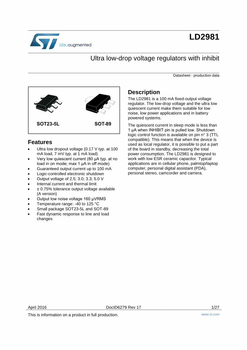
LD2981
Ultra low-drop voltage regulators with inhibit
Datasheet - production data
Features Ultra low dropout voltage (0.17 V typ. at 100
mA load, 7 mV typ. at 1 mA load)
Very low quiescent current (80 μA typ. at no load in on mode; max 1 μA in off mode)
Guaranteed output current up to 100 mA
Logic-controlled electronic shutdown
Output voltage of 2.5; 3.0; 3.3; 5.0 V
Internal current and thermal limit
± 0.75% tolerance output voltage available (A version)
Output low noise voltage 160 μVRMS
Temperature range: -40 to 125 °C
Small package SOT23-5L and SOT-89
Fast dynamic response to line and load changes
Description The LD2981 is a 100 mA fixed-output voltage regulator. The low-drop voltage and the ultra low quiescent current make them suitable for low noise, low power applications and in battery powered systems.
The quiescent current in sleep mode is less than 1 μA when INHIBIT pin is pulled low. Shutdown logic control function is available on pin n° 3 (TTL compatible). This means that when the device is used as local regulator, it is possible to put a part of the board in standby, decreasing the total power consumption. The LD2981 is designed to work with low ESR ceramic capacitor. Typical applications are in cellular phone, palmtop/laptop computer, personal digital assistant (PDA), personal stereo, camcorder and camera.
Contents LD2981
2/27 DocID6279 Rev 17
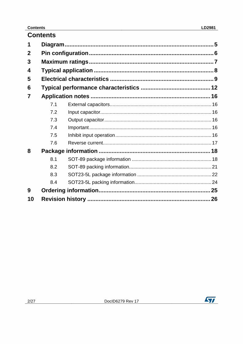
Contents
1 Diagram ............................................................................................ 5
2 Pin configuration ............................................................................. 6
3 Maximum ratings ............................................................................. 7
4 Typical application .......................................................................... 8
5 Electrical characteristics ................................................................ 9
6 Typical performance characteristics ........................................... 12
7 Application notes .......................................................................... 16
7.1 External capacitors .......................................................................... 16
7.2 Input capacitor ................................................................................. 16
7.3 Output capacitor .............................................................................. 16
7.4 Important ......................................................................................... 16
7.5 Inhibit input operation ...................................................................... 16
7.6 Reverse current ............................................................................... 17
8 Package information ..................................................................... 18
8.1 SOT-89 package information .......................................................... 18
8.2 SOT-89 packing information............................................................ 21
8.3 SOT23-5L package information ...................................................... 22
8.4 SOT23-5L packing information ........................................................ 24
9 Ordering information ..................................................................... 25
10 Revision history ............................................................................ 26

LD2981 List of tables
DocID6279 Rev 17 3/27
List of tables
Table 1: Pin description .............................................................................................................................. 6 Table 2: Thermal data ................................................................................................................................. 6 Table 3: Absolute maximum ratings ........................................................................................................... 7 Table 4: Electrical characteristics for LD2981AB ....................................................................................... 9 Table 5: Electrical characteristics for LD2981C ........................................................................................ 10 Table 6: SOT-89 mechanical data ............................................................................................................ 19 Table 7: SOT-89 carrier tape mechanical data ......................................................................................... 21 Table 8: SOT23-5L package mechanical data ......................................................................................... 22 Table 9: SOT23-5L tape and reel mechanical data .................................................................................. 24 Table 10: Order codes .............................................................................................................................. 25 Table 11: Document revision history ........................................................................................................ 26

List of figures LD2981
4/27 DocID6279 Rev 17
List of figures
Figure 1: Schematic diagram ...................................................................................................................... 5 Figure 2: Pin connections (top view) ........................................................................................................... 6 Figure 3: Application circuit ......................................................................................................................... 8 Figure 4: Output voltage vs temperature .................................................................................................. 12 Figure 5: Dropout voltage vs temperature ................................................................................................ 12 Figure 6: Line regulation vs temperature .................................................................................................. 12 Figure 7: Load regulation vs temperature ................................................................................................. 12 Figure 8: Dropout voltage vs temperature ................................................................................................ 13 Figure 9: Quiescent current vs temperature ............................................................................................. 13 Figure 10: Quiescent current vs output current ........................................................................................ 13 Figure 11: Off mode quiescent current vs temperature ............................................................................ 13 Figure 12: Quiescent current vs input voltage .......................................................................................... 13 Figure 13: Dropout voltage vs output current ........................................................................................... 13 Figure 14: Inhibit input current vs temperature ......................................................................................... 14 Figure 15: Inhibit voltage vs temperature ................................................................................................. 14 Figure 16: Supply voltage rejection vs frequency ..................................................................................... 14 Figure 17: Noise voltage vs frequency ..................................................................................................... 14 Figure 18: Best case: highest output version ........................................................................................... 14 Figure 19: Worst case: lowest output version ........................................................................................... 14 Figure 20: Load transient response .......................................................................................................... 15 Figure 21: Line transient response ........................................................................................................... 15 Figure 22: Reverse current test circuit ...................................................................................................... 17 Figure 23: SOT-89 package outline .......................................................................................................... 18 Figure 24: SOT-89 recommended footprint .............................................................................................. 20 Figure 25: SOT-89 carrier tape outline ..................................................................................................... 21 Figure 26: SOT23-5L package outline ...................................................................................................... 22 Figure 27: SOT23-5L recommended footprint .......................................................................................... 23 Figure 28: SOT23-5L tape and reel outline .............................................................................................. 24

LD2981 Diagram
DocID6279 Rev 17 5/27
1 Diagram Figure 1: Schematic diagram

Pin configuration LD2981
6/27 DocID6279 Rev 17
2 Pin configuration Figure 2: Pin connections (top view)
Table 1: Pin description
Pin n°
SOT23-5L
Pin n°
SOT-89 Symbol Name and function
1 3 VIN Input port
2 2 GND Ground pin
3
INHIBIT
Control switch ON/OFF. Inhibit is not internally pulled-up; it cannot be left floating. Disable the device when connected to GND or to a positive voltage less than 0.18 V
4
NC Not connected
5 1 VOUT Output port
Table 2: Thermal data
Symbol Parameter SOT23-5L SOT-89 Unit
RthJC Thermal resistance junction-case 81 15 °C/W
RthJA Thermal resistance junction-ambient 255 110 °C/W

LD2981 Maximum ratings
DocID6279 Rev 17 7/27
3 Maximum ratings Table 3: Absolute maximum ratings
Symbol Parameter Value Unit
VI DC input voltage -0.3 to 16 V
VINH INHIBIT input voltage -0.3 to 16 V
IO Output current Internally limited
PD Power dissipation Internally limited
TSTG Storage temperature range -55 to 150 °C
TOP Operating junction temperature range -40 to 125 °C
Absolute maximum ratings are those values beyond which damage to the device may occur. Functional operation under these condition is not implied.

Typical application LD2981
8/27 DocID6279 Rev 17
4 Typical application Figure 3: Application circuit
Inhibit pin is not internally pulled-up then it must not be left floating. Disable the device when connected to GND or to a positive voltage less than 0.18 V.
LD2981 Electrical characteristics
DocID6279 Rev 17 9/27
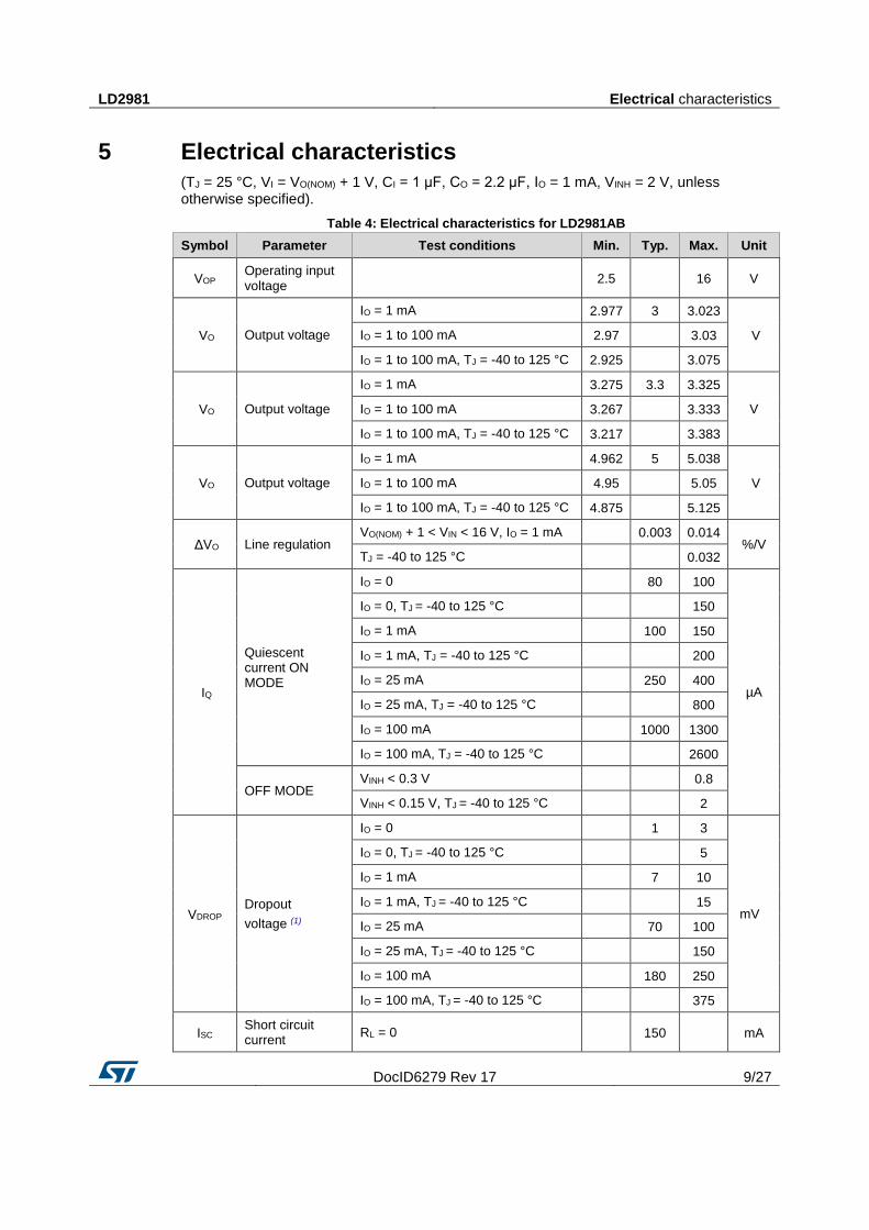
5 Electrical characteristics
(TJ = 25 °C, VI = VO(NOM) + 1 V, CI = 1 μF, CO = 2.2 μF, IO = 1 mA, VINH = 2 V, unless otherwise specified).
Table 4: Electrical characteristics for LD2981AB
Symbol Parameter Test conditions Min. Typ. Max. Unit
VOP Operating input voltage
2.5
16 V
VO Output voltage
IO = 1 mA 2.977 3 3.023
V IO = 1 to 100 mA 2.97
3.03
IO = 1 to 100 mA, TJ = -40 to 125 °C 2.925
3.075
VO Output voltage
IO = 1 mA 3.275 3.3 3.325
V IO = 1 to 100 mA 3.267
3.333
IO = 1 to 100 mA, TJ = -40 to 125 °C 3.217
3.383
VO Output voltage
IO = 1 mA 4.962 5 5.038
V IO = 1 to 100 mA 4.95
5.05
IO = 1 to 100 mA, TJ = -40 to 125 °C 4.875
5.125
ΔVO Line regulation VO(NOM) + 1 < VIN < 16 V, IO = 1 mA
0.003 0.014
%/V TJ = -40 to 125 °C
0.032
IQ
Quiescent current ON MODE
IO = 0
80 100
µA
IO = 0, TJ = -40 to 125 °C
150
IO = 1 mA
100 150
IO = 1 mA, TJ = -40 to 125 °C
200
IO = 25 mA
250 400
IO = 25 mA, TJ = -40 to 125 °C
800
IO = 100 mA
1000 1300
IO = 100 mA, TJ = -40 to 125 °C
2600
OFF MODE VINH < 0.3 V
0.8
VINH < 0.15 V, TJ = -40 to 125 °C
2
VDROP Dropout
voltage (1)
IO = 0
1 3
mV
IO = 0, TJ = -40 to 125 °C
5
IO = 1 mA
7 10
IO = 1 mA, TJ = -40 to 125 °C
15
IO = 25 mA
70 100
IO = 25 mA, TJ = -40 to 125 °C
150
IO = 100 mA
180 250
IO = 100 mA, TJ = -40 to 125 °C
375
ISC Short circuit current
RL = 0
150
mA

Electrical characteristics LD2981
10/27 DocID6279 Rev 17
Symbol Parameter Test conditions Min. Typ. Max. Unit
SVR Supply voltage rejection
CO = 10 µF, f = 1 KHz
63
dB
VINH Inhibit input logic low
LOW = Output OFF,
TJ = -40 to 125 °C 0.18 V
VINL Inhibit input logic high
HIGH = Output ON,
TJ = -40 to 125 °C 1.6
V
IINH Inhibit input current
VINH = 0 V, TJ = -40 to 125 °C
0 -1 µA
VINH = 5 V, TJ = -40 to 125 °C
5 15
eN Output noise voltage
BW = 300 Hz to 50 KHz, CO = 10 µF
160
µVRMS
TSHDN Thermal shutdown
170
°C
Notes:
(1) For VO < 2.5 V dropout voltage can be calculated according to the minimum input voltage in full temperature range.
(TJ = 25 °C, VI = VO(NOM) +1 V, CI = 1 μF, CO = 2.2 μF, IO = 1 mA, VINH = 2 V, unless otherwise specified)
Table 5: Electrical characteristics for LD2981C
Symbol Parameter Test conditions Min. Typ. Max. Unit
VOP Operating input voltage
2.5
16 V
VO Output voltage
IO = 1 mA 2.468 2.5 2.531
V IO = 1 to 100 mA 2.45
2.55
IO = 1 to 100 mA, TJ = -40 to 125 °C 2.412
2.587
VO Output voltage
IO = 1 mA 2.962 3 3.037
V IO = 1 to 100 mA 2.94
3.06
IO = 1 to 100 mA, TJ = -40 to 125 °C 2.895
3.105
VO Output voltage
IO = 1 mA 3.258 3.3 3.341
V IO = 1 to 100 mA 3.234
3.366
IO = 1 to 100 mA, TJ = -40 to 125 °C 3.184
3.415
VO Output voltage
IO = 1 mA 4.937 5 5.062
V IO = 1 to 100 mA 4.9
5.1
IO = 1 to 100 mA, TJ = -40 to 125 °C 4.825
5.175
ΔVO Line regulation VO(NOM) + 1 < VIN < 16 V, IO = 1 mA
0.003 0.014
%/V TJ = -40 to 125 °C
0.032

LD2981 Electrical characteristics
DocID6279 Rev 17 11/27
Symbol Parameter Test conditions Min. Typ. Max. Unit
IQ
Quiescent current
ON MODE
IO = 0
80 100
µA
IO = 0, TJ = -40 to 125 °C
150
IO = 1 mA
100 150
IO = 1 mA, TJ = -40 to 125 °C
200
IO = 25 mA
250 400
IO = 25 mA, TJ = -40 to 125 °C
800
IO = 100 mA
1000 1300
IO = 100 mA, TJ = -40 to 125 °C
2600
OFF MODE VINH < 0.3 V
0.8
VINH < 0.15 V, TJ = -40 to 125 °C
2
VDROP Dropout
voltage (1)
IO = 0
1 3
mV
IO = 0, TJ = -40 to 125 °C
5
IO = 1 mA
7 10
IO = 1 mA, TJ = -40 to 125 °C
15
IO = 25 mA
70 100
IO = 25 mA, TJ = -40 to 125 °C
150
IO = 100 mA
180 250
IO = 100 mA, TJ = -40 to 125 °C
375
ISC Short circuit current
RL = 0
150
mA
SVR Supply voltage rejection
CO = 10 µF, f = 1 KHz
63
dB
VINH Inhibit input logic low
LOW = Output OFF,
TJ = -40 to 125 °C 0.18 V
VINL Inhibit input logic high
HIGH = Output ON,
TJ = -40 to 125 °C 1.6
V
IINH Inhibit input current
VINH = 0 V, TJ = -40 to 125 °C
0 -1 μF
VINH = 5 V, TJ = -40 to 125 °C
5 15
eN Output noise voltage
BW = 300 Hz to 50 KHz, CO = 10 µF
160
µVRMS
TSHDN Thermal shutdown
170
°C
Notes:
(1) For VO < 2.5 V dropout voltage can be calculated according to the minimum input voltage in full temperature range.

Typical performance characteristics LD2981
12/27 DocID6279 Rev 17
6 Typical performance characteristics
(TJ = 25 °C, VI = VO(NOM) +1 V, CI = 1 μF, CO = 2.2 μF, VINH = 2 V, unless otherwise specified).
Figure 4: Output voltage vs temperature
Figure 5: Dropout voltage vs temperature
Figure 6: Line regulation vs temperature
Figure 7: Load regulation vs temperature

LD2981 Typical performance characteristics
DocID6279 Rev 17 13/27
Figure 8: Dropout voltage vs temperature
Figure 9: Quiescent current vs temperature
Figure 10: Quiescent current vs output current
Figure 11: Off mode quiescent current vs temperature
Figure 12: Quiescent current vs input voltage
Figure 13: Dropout voltage vs output current

Typical performance characteristics LD2981
14/27 DocID6279 Rev 17
Figure 14: Inhibit input current vs temperature
Figure 15: Inhibit voltage vs temperature
Figure 16: Supply voltage rejection vs frequency
Figure 17: Noise voltage vs frequency
Figure 18: Best case: highest output version
Figure 19: Worst case: lowest output version

LD2981 Typical performance characteristics
DocID6279 Rev 17 15/27
Figure 20: Load transient response
Figure 21: Line transient response

Application notes LD2981
16/27 DocID6279 Rev 17
7 Application notes
7.1 External capacitors
Like any low-dropout regulator, the LD2981 requires external capacitors for regulator stability. This capacitor must be selected to meet the requirements of minimum capacitance and equivalent series resistance. We suggest to solder input and output capacitors as close as possible to the relative pins.
7.2 Input capacitor
An input capacitor whose value is 1 μF is required with the LD2981 (amount of capacitance can be increased without limit). This capacitor must be located a distance of not more than 0.5" from the input pin of the device and returned to a clean analog ground. Any good quality ceramic, tantalum or film capacitors can be used for this capacitor.
7.3 Output capacitor
The LD2981 is designed specifically to work with ceramic output capacitors. It may also be possible to use Tantalum capacitors, but these are not as attractive for reasons of size and cost. By the way, the output capacitor must meet both the requirement for minimum amount of capacitance and ESR (equivalent series resistance) value. The Figure 18: "Best case: highest output version" and Figure 19: "Worst case: lowest output version" show the allowable ESR range as a function of the output capacitance. These curves represent the stability region over the full temperature and IO range. Due to the different loop gain, the stability improves for higher output versions and so the suggested minimum output capacitor value, if low ESR ceramic type is used, is 1 μF for output voltages equal or major than 3.8 V, 2.2 μF for output voltages from 2.85 to 3.3 V, and 3.3 μF for the other versions. However, if an output capacitor lower than the suggested one is used, it’s possible to make stable the regulator adding a resistor in series to the capacitor (see Figure 18: "Best case: highest output version" and Figure 19: "Worst case: lowest output version" to choose the right value according to the used version and keeping in account that the ESR of ceramic capacitors has been measured @ 100 kHz).
7.4 Important
The output capacitor must maintain its ESR in the stable region over the full operating temperature to assure stability. Also, capacitor tolerance and variation with temperature must be considered to assure the minimum amount of capacitance is provided at all times. This capacitor should be located not more than 0.5" from the output pin of the device and returned to a clean analog ground.
7.5 Inhibit input operation
The inhibit pin can be used to turn OFF the regulator when pulled low, so drastically reducing the current consumption down to less than 1 μA. When the inhibit feature is not used, this pin must be tied to VI to keep the regulator output ON at all times. To assure proper operation, the signal source used to drive the inhibit pin must be able to swing above and below the specified thresholds listed in the electrical characteristics section under VIH VIL. Any slew rate can be used to drive the inhibit.
LD2981 Application notes
DocID6279 Rev 17 17/27
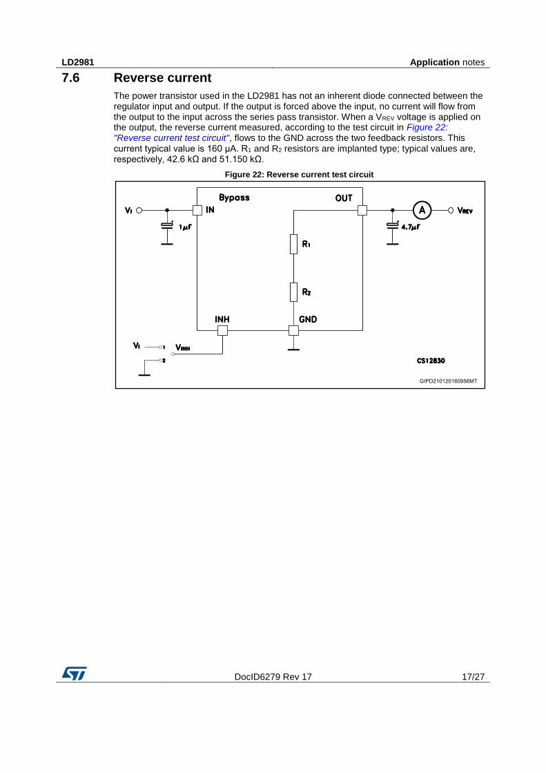
7.6 Reverse current
The power transistor used in the LD2981 has not an inherent diode connected between the regulator input and output. If the output is forced above the input, no current will flow from the output to the input across the series pass transistor. When a VREV voltage is applied on the output, the reverse current measured, according to the test circuit in Figure 22: "Reverse current test circuit", flows to the GND across the two feedback resistors. This current typical value is 160 μA. R1 and R2 resistors are implanted type; typical values are, respectively, 42.6 kΩ and 51.150 kΩ.
Figure 22: Reverse current test circuit

Package information LD2981
18/27 DocID6279 Rev 17
8 Package information
In order to meet environmental requirements, ST offers these devices in different grades of ECOPACK® packages, depending on their level of environmental compliance. ECOPACK® specifications, grade definitions and product status are available at: www.st.com. ECOPACK® is an ST trademark.
8.1 SOT-89 package information
Figure 23: SOT-89 package outline
LD2981 Package information
DocID6279 Rev 17 19/27
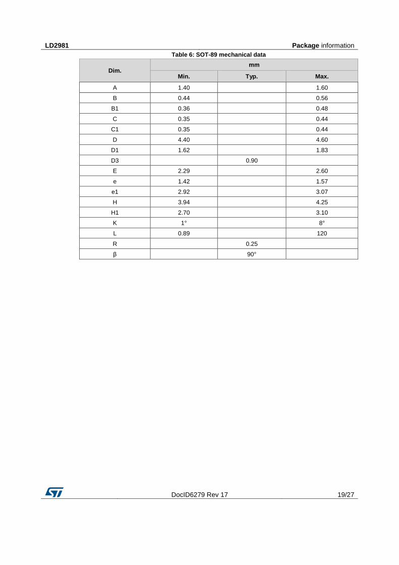
Table 6: SOT-89 mechanical data
Dim. mm
Min. Typ. Max.
A 1.40
1.60
B 0.44
0.56
B1 0.36
0.48
C 0.35
0.44
C1 0.35
0.44
D 4.40
4.60
D1 1.62
1.83
D3
0.90
E 2.29
2.60
e 1.42
1.57
e1 2.92
3.07
H 3.94
4.25
H1 2.70
3.10
K 1°
8°
L 0.89
120
R
0.25
β
90°

Package information LD2981
20/27 DocID6279 Rev 17
Figure 24: SOT-89 recommended footprint

LD2981 Package information
DocID6279 Rev 17 21/27
8.2 SOT-89 packing information
Figure 25: SOT-89 carrier tape outline
Table 7: SOT-89 carrier tape mechanical data
Dim. mm
Value Tolerance
Ao 4.91 ± 0.10
Bo 4.52 ± 0.10
Ko 1.90 ± 0.10
F 5.50 ± 0.10
E 1.75 ± 0.10
W 12 ± 0.30
P2 2 ± 0.10
Po 4 ± 0.10
P1 8 ± 0.10
T 0.30 ± 0.10
D Ø 1.55 ± 0.05
D1 Ø 1.60 ± 0.10

Package information LD2981
22/27 DocID6279 Rev 17
8.3 SOT23-5L package information
Figure 26: SOT23-5L package outline
Table 8: SOT23-5L package mechanical data
Dim. mm
Min. Typ. Max.
A 0.90
1.45
A1 0
0.15
A2 0.90
1.30
b 0.30
0.50
c 0.09
0.20
D
2.95
E
1.60
e
0.95
H
2.80
L 0.30
0.60
θ 0°
8°

LD2981 Package information
DocID6279 Rev 17 23/27
Figure 27: SOT23-5L recommended footprint
Dimensions are in mm

Package information LD2981
24/27 DocID6279 Rev 17
8.4 SOT23-5L packing information
Figure 28: SOT23-5L tape and reel outline
Table 9: SOT23-5L tape and reel mechanical data
Dim. mm
Min. Typ. Max.
A
180
C 12.8 13.0 13.2
D 20.2
N 60
T
14.4
Ao 3.13 3.23 3.33
Bo 3.07 3.17 3.27
Ko 1.27 1.37 1.47
Po 3.9 4.0 4.1
P 3.9 4.0 4.1
Bo
Ko Ao
Po
P
DA N
T

LD2981 Ordering information
DocID6279 Rev 17 25/27
9 Ordering information Table 10: Order codes
AB version C version Output voltage
SOT23-5L SOT-89 SOT23-5L SOT-89
LD2981CM25TR
2.5 V
LD2981ABM30TR
LD2981CM30TR
3.0 V
LD2981ABM33TR LD2981ABU33TR LD2981CM33TR LD2981CU33TR 3.3 V
LD2981ABM50TR LD2981ABU50TR LD2981CM33TR LD2981CU50TR 5.0 V
Revision history LD2981
26/27 DocID6279 Rev 17
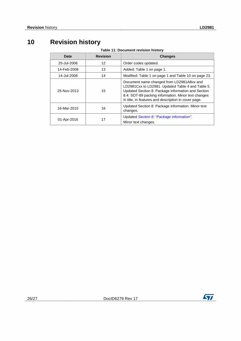
10 Revision history Table 11: Document revision history
Date Revision Changes
25-Jul-2006 12 Order codes updated.
14-Feb-2008 13 Added: Table 1 on page 1.
14-Jul-2008 14 Modified: Table 1 on page 1 and Table 10 on page 23.
25-Nov-2013 15
Document name changed from LD2981ABxx and
LD2981Cxx to LD2981. Updated Table 4 and Table 5.
Updated Section 8: Package information and Section
8.4: SOT-89 packing information. Minor text changes
in title, in features and description in cover page.
16-Mar-2015 16 Updated Section 8: Package information. Minor text
changes.
01-Apr-2016 17 Updated Section 8: "Package information".
Minor text changes.

LD2981
DocID6279 Rev 17 27/27
IMPORTANT NOTICE – PLEASE READ CAREFULLY
STMicroelectronics NV and its subsidiaries (“ST”) reserve the right to make changes, corrections, enhancements, modifications , and improvements to ST products and/or to this document at any time without notice. Purchasers should obtain the latest relevant information on ST products before placing orders. ST products are sold pursuant to ST’s terms and conditions of sale in place at the time of order acknowledgement.
Purchasers are solely responsible for the choice, selection, and use of ST products and ST assumes no liability for application assistance or the design of Purchasers’ products.
No license, express or implied, to any intellectual property right is granted by ST herein.
Resale of ST products with provisions different from the information set forth herein shall void any warranty granted by ST for such product.
ST and the ST logo are trademarks of ST. All other product or service names are the property of their respective owners.
Information in this document supersedes and replaces information previously supplied in any prior versions of this document.
© 2016 STMicroelectronics – All rights reserved


![SINDBAD THE SAILOR · Web view[3.105] When the Indians reach the place where the gold is, they fill their bags with the sand, and ride away at their best speed: the ants, however,](https://img.pdfslide.us/doc/110x75/5e270ab367370301e77d1e8a/sindbad-the-sailor-web-view-3105-when-the-indians-reach-the-place-where-the-gold.jpg)