Embed Size (px)
Citation preview
This is information on a product in full production.
January 2014 DocID9587 Rev 15 1/22
LD3985
Ultra low drop and low noise BiCMOS voltage regulators
Datasheet - production data
Features• Input voltage from 2.5 V to 6 V
• Stable with low ESR ceramic capacitors
• Ultra low-dropout voltage (60 mV typ. at 150 mA load, 0.4 mV typ. at 1 mA load)
• Very low quiescent current (85 µA typ. at no load, 170 µA typ. at 150 mA load; max.1.5 µA in OFF mode)
• Guaranteed output current up to 150 mA
• Wide range of output voltage: 1.22 V; 1.8 V; 2.5 V; 2.6 V; 2.7 V; 2.8 V; 2.9 V; 3 V; 3.3 V; 4.7 V
• Fast turn-on time: typ. 200 µs [CO = 1 µF, CBYP = 10 nF and IO = 1 mA]
• Logic-controlled electronic shutdown
• Internal current and thermal limit
• Output low noise voltage 30 µVRMS over 10 Hz to 100 kHz
• SVR of 60 dB at 1 kHz, 50 dB at 10 kHz
• Temperature range: - 40 °C to 125 °C
DescriptionThe LD3985 provides up to 150 mA, from 2.5 V to 6 V input voltage. The ultra low drop voltage, low quiescent current and low noise make it suitable for low power applications and in battery-powered systems. Regulator ground current increases slightly in dropout only, prolonging the battery life. Power supply rejection is better than 60 dB at low frequencies and rolls off at 10 kHz. High power supply rejection is maintained down to low input voltage levels common to battery operated circuits. Shutdown logic control function is available, this means that when the device is used as local regulator, it is possible to put a part of the board in standby, decreasing the total power consumption. The LD3985 is designed to work with low ESR ceramic capacitors. Typical applications are in mobile phones and similar battery-powered wireless systems.
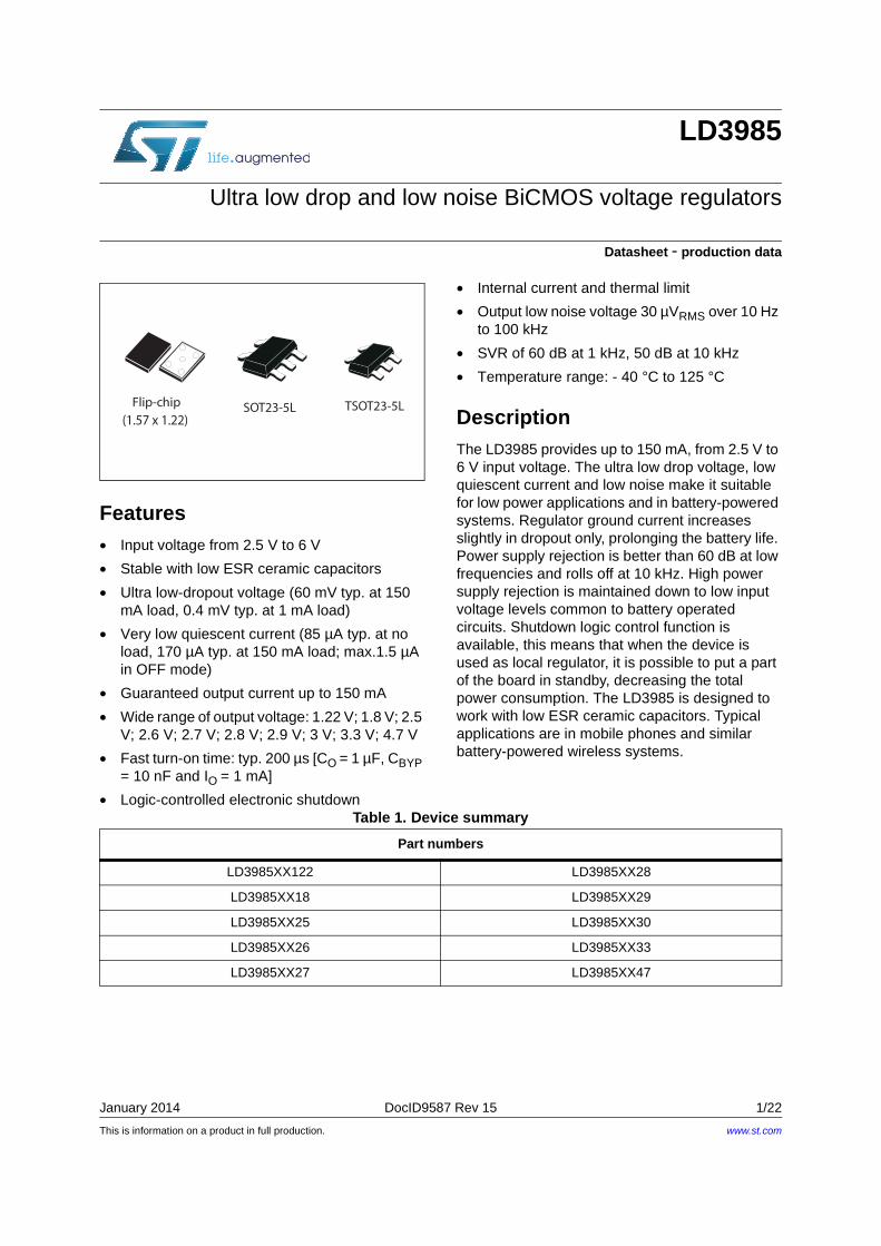
Flip-chip SOT23-5L TSOT23-5L(1.57 x 1.22)
Table 1. Device summary
Part numbers
LD3985XX122 LD3985XX28
LD3985XX18 LD3985XX29
LD3985XX25 LD3985XX30
LD3985XX26 LD3985XX33
LD3985XX27 LD3985XX47
www.st.com
Contents LD3985
2/22 DocID9587 Rev 15
Contents
1 Diagram . . . . . . . . . . . . . . . . . . . . . . . . . . . . . . . . . . . . . . . . . . . . . . . . . . . 3
2 Pin configuration . . . . . . . . . . . . . . . . . . . . . . . . . . . . . . . . . . . . . . . . . . . . 4
3 Typical application . . . . . . . . . . . . . . . . . . . . . . . . . . . . . . . . . . . . . . . . . . 5
4 Maximum ratings . . . . . . . . . . . . . . . . . . . . . . . . . . . . . . . . . . . . . . . . . . . . 6
5 Electrical characteristics . . . . . . . . . . . . . . . . . . . . . . . . . . . . . . . . . . . . . 7
6 Typical performance characteristics . . . . . . . . . . . . . . . . . . . . . . . . . . . . 9
7 Package mechanical data . . . . . . . . . . . . . . . . . . . . . . . . . . . . . . . . . . . . 13
8 Packaging mechanical data . . . . . . . . . . . . . . . . . . . . . . . . . . . . . . . . . . 18
9 Order codes . . . . . . . . . . . . . . . . . . . . . . . . . . . . . . . . . . . . . . . . . . . . . . . 20
10 Revision history . . . . . . . . . . . . . . . . . . . . . . . . . . . . . . . . . . . . . . . . . . . 21
DocID9587 Rev 15 3/22
LD3985 Diagram
22
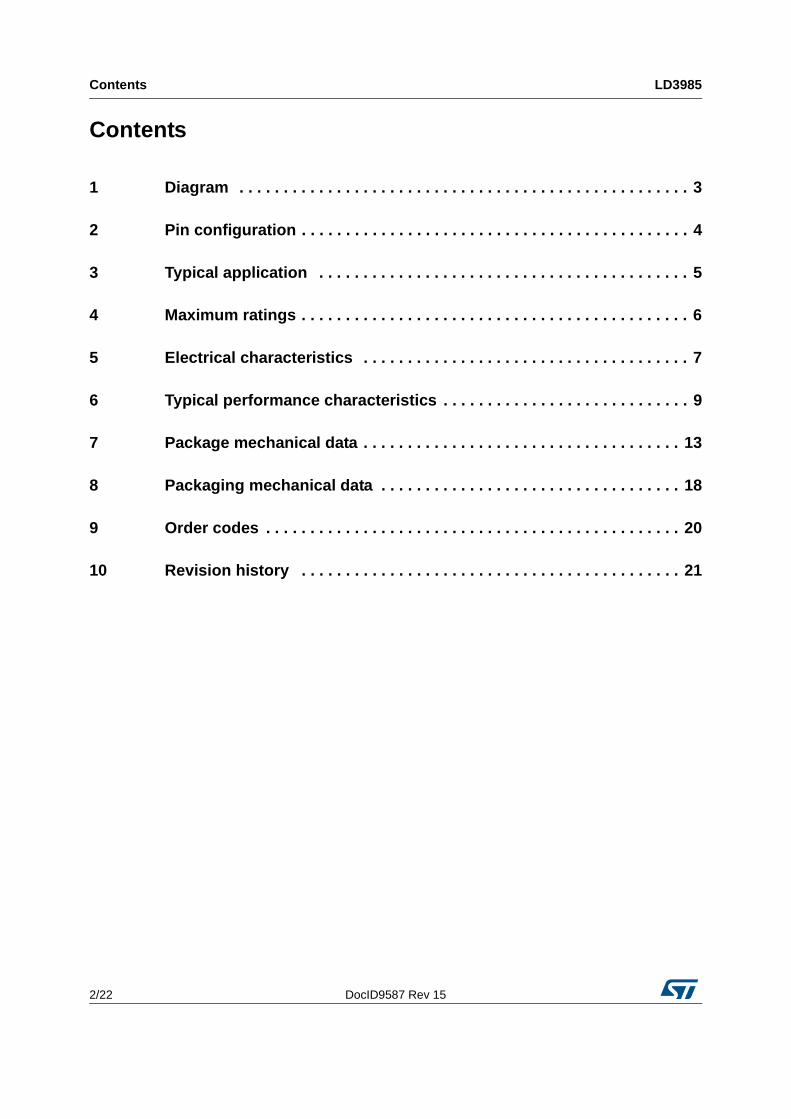
1 Diagram
Figure 1. Schematic diagram
Pin configuration LD3985
4/22 DocID9587 Rev 15
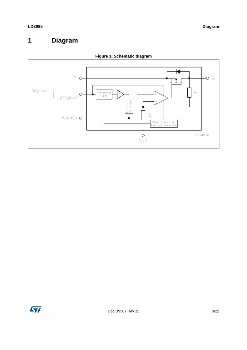
2 Pin configuration
Figure 2. Pin connections (SOT and TSOT top view, Flip-chip top view)
Flip-chipSOT23-5L/TSOT23-5L
Table 2. Pin description
Pin n° for SOT23-5L/
TSOT23-5L
Pin n° for Flip-chip
Symbol Name and function
1 4 VI Input voltage of the LDO
2 2 GND Common ground
3 1 VINHInhibit input voltage: ON mode when VINH ≥ 1.2 V, OFF mode when VINH ≤ 0.4 V (Do not leave it floating, not internally pulled down/up)
4 5 BYPASSBypass pin: an external capacitor (usually 10 nF) has to be connected to minimize noise voltage
5 3 VO Output voltage of the LDO
DocID9587 Rev 15 5/22
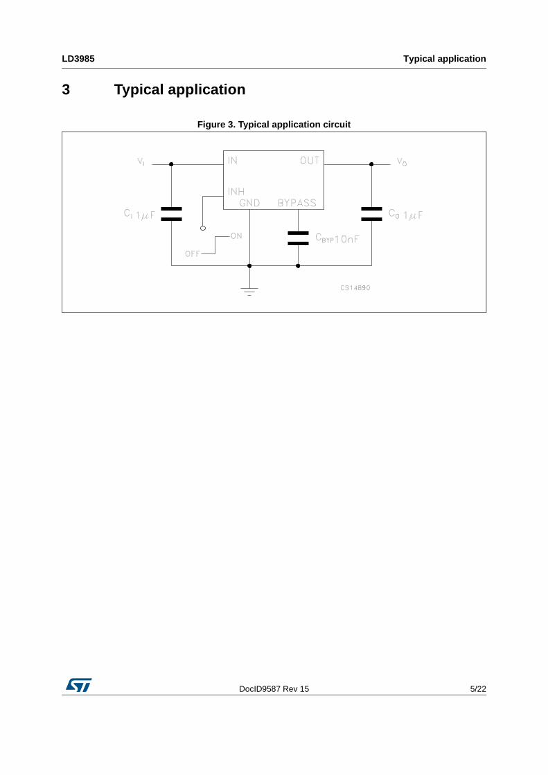
LD3985 Typical application
22
3 Typical application
Figure 3. Typical application circuit
Maximum ratings LD3985
6/22 DocID9587 Rev 15
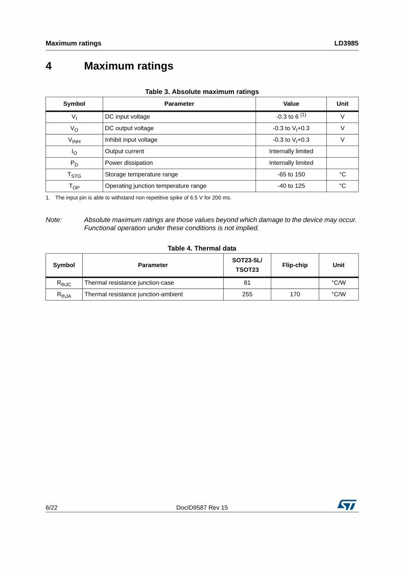
4 Maximum ratings
Note: Absolute maximum ratings are those values beyond which damage to the device may occur. Functional operation under these conditions is not implied.
Table 3. Absolute maximum ratings
Symbol Parameter Value Unit
VI DC input voltage -0.3 to 6 (1)
1. The input pin is able to withstand non repetitive spike of 6.5 V for 200 ms.
V
VO DC output voltage -0.3 to VI+0.3 V
VINH Inhibit input voltage -0.3 to VI+0.3 V
IO Output current Internally limited
PD Power dissipation Internally limited
TSTG Storage temperature range -65 to 150 °C
TOP Operating junction temperature range -40 to 125 °C
Table 4. Thermal data
Symbol ParameterSOT23-5L/
TSOT23Flip-chip Unit
RthJC Thermal resistance junction-case 81 °C/W
RthJA Thermal resistance junction-ambient 255 170 °C/W
DocID9587 Rev 15 7/22
LD3985 Electrical characteristics
22
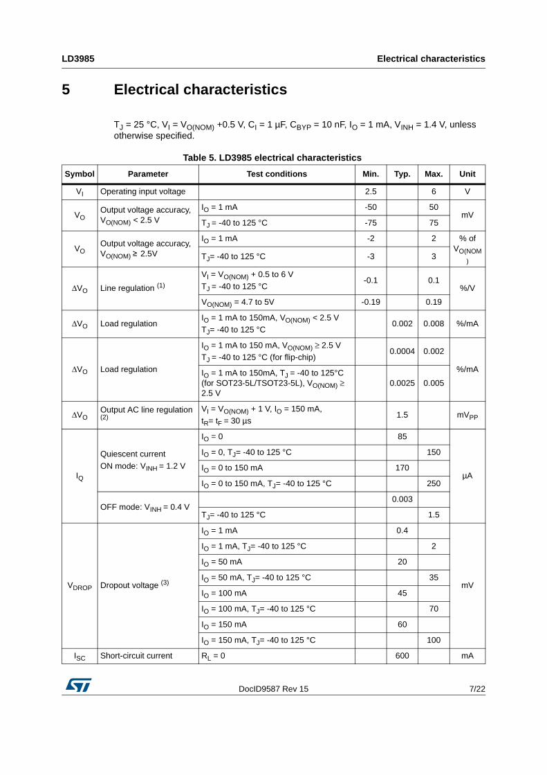
5 Electrical characteristics
TJ = 25 °C, VI = VO(NOM) +0.5 V, CI = 1 µF, CBYP = 10 nF, IO = 1 mA, VINH = 1.4 V, unless otherwise specified.
Table 5. LD3985 electrical characteristics
Symbol Parameter Test conditions Min. Typ. Max. Unit
VI Operating input voltage 2.5 6 V
VOOutput voltage accuracy, VO(NOM) < 2.5 V
IO = 1 mA -50 50mV
TJ = -40 to 125 °C -75 75
VOOutput voltage accuracy, VO(NOM) ≥ 2.5V
IO = 1 mA -2 2 % ofVO(NOM
)TJ= -40 to 125 °C -3 3
ΔVO Line regulation (1)
VI = VO(NOM) + 0.5 to 6 V
TJ = -40 to 125 °C-0.1 0.1
%/V
VO(NOM) = 4.7 to 5V -0.19 0.19
ΔVO Load regulationIO = 1 mA to 150mA, VO(NOM) < 2.5 VTJ= -40 to 125 °C
0.002 0.008 %/mA
ΔVO Load regulation
IO = 1 mA to 150 mA, VO(NOM) ≥ 2.5 VTJ = -40 to 125 °C (for flip-chip)
0.0004 0.002
%/mAIO = 1 mA to 150mA, TJ = -40 to 125°C (for SOT23-5L/TSOT23-5L), VO(NOM) ≥ 2.5 V
0.0025 0.005
ΔVOOutput AC line regulation (2)
VI = VO(NOM) + 1 V, IO = 150 mA,tR= tF = 30 µs
1.5 mVPP
IQ
Quiescent current
ON mode: VINH = 1.2 V
IO = 0 85
µA
IO = 0, TJ= -40 to 125 °C 150
IO = 0 to 150 mA 170
IO = 0 to 150 mA, TJ= -40 to 125 °C 250
OFF mode: VINH = 0.4 V0.003
TJ= -40 to 125 °C 1.5
VDROP Dropout voltage (3)
IO = 1 mA 0.4
mV
IO = 1 mA, TJ= -40 to 125 °C 2
IO = 50 mA 20
IO = 50 mA, TJ= -40 to 125 °C 35
IO = 100 mA 45
IO = 100 mA, TJ= -40 to 125 °C 70
IO = 150 mA 60
IO = 150 mA, TJ= -40 to 125 °C 100
ISC Short-circuit current RL = 0 600 mA
Electrical characteristics LD3985
8/22 DocID9587 Rev 15
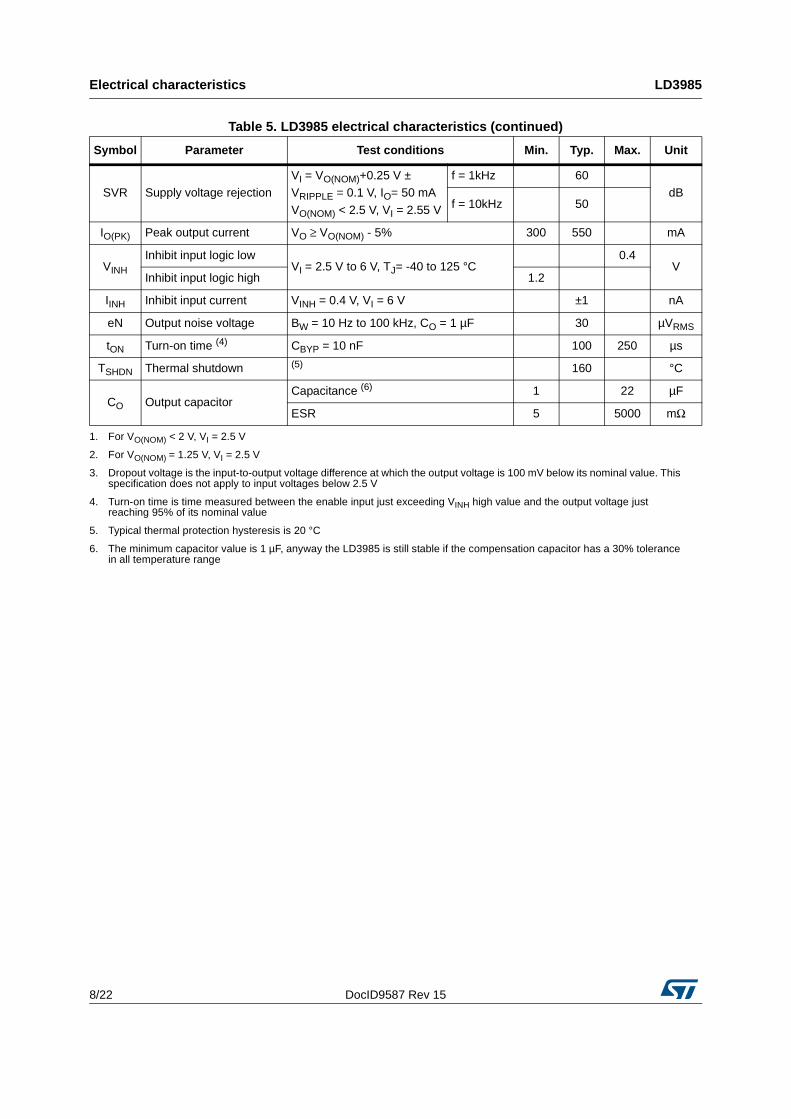
SVR Supply voltage rejectionVI = VO(NOM)+0.25 V ±VRIPPLE = 0.1 V, IO= 50 mA
VO(NOM) < 2.5 V, VI = 2.55 V
f = 1kHz 60dB
f = 10kHz 50
IO(PK) Peak output current VO ≥ VO(NOM) - 5% 300 550 mA
VINH
Inhibit input logic lowVI = 2.5 V to 6 V, TJ= -40 to 125 °C
0.4V
Inhibit input logic high 1.2
IINH Inhibit input current VINH = 0.4 V, VI = 6 V ±1 nA
eN Output noise voltage BW = 10 Hz to 100 kHz, CO = 1 µF 30 µVRMS
tON Turn-on time (4) CBYP = 10 nF 100 250 µs
TSHDN Thermal shutdown (5) 160 °C
CO Output capacitorCapacitance (6) 1 22 µF
ESR 5 5000 mΩ
1. For VO(NOM) < 2 V, VI = 2.5 V
2. For VO(NOM) = 1.25 V, VI = 2.5 V
3. Dropout voltage is the input-to-output voltage difference at which the output voltage is 100 mV below its nominal value. This specification does not apply to input voltages below 2.5 V
4. Turn-on time is time measured between the enable input just exceeding VINH high value and the output voltage just reaching 95% of its nominal value
5. Typical thermal protection hysteresis is 20 °C
6. The minimum capacitor value is 1 µF, anyway the LD3985 is still stable if the compensation capacitor has a 30% tolerance in all temperature range
Table 5. LD3985 electrical characteristics (continued)
Symbol Parameter Test conditions Min. Typ. Max. Unit
DocID9587 Rev 15 9/22
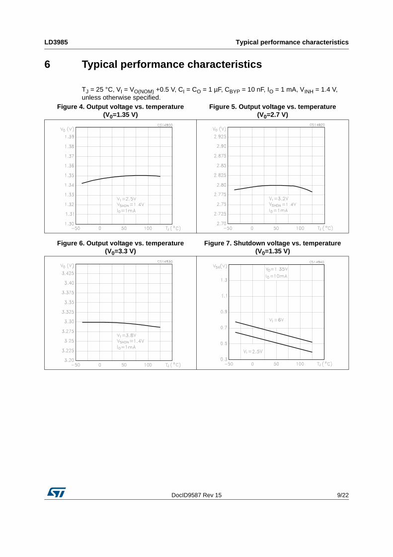
LD3985 Typical performance characteristics
22
6 Typical performance characteristics
TJ = 25 °C, VI = VO(NOM) +0.5 V, CI = CO = 1 µF, CBYP = 10 nF, IO = 1 mA, VINH = 1.4 V, unless otherwise specified.
Figure 4. Output voltage vs. temperature (V0=1.35 V)
Figure 5. Output voltage vs. temperature (V0=2.7 V)
Figure 6. Output voltage vs. temperature (V0=3.3 V)
Figure 7. Shutdown voltage vs. temperature (V0=1.35 V)
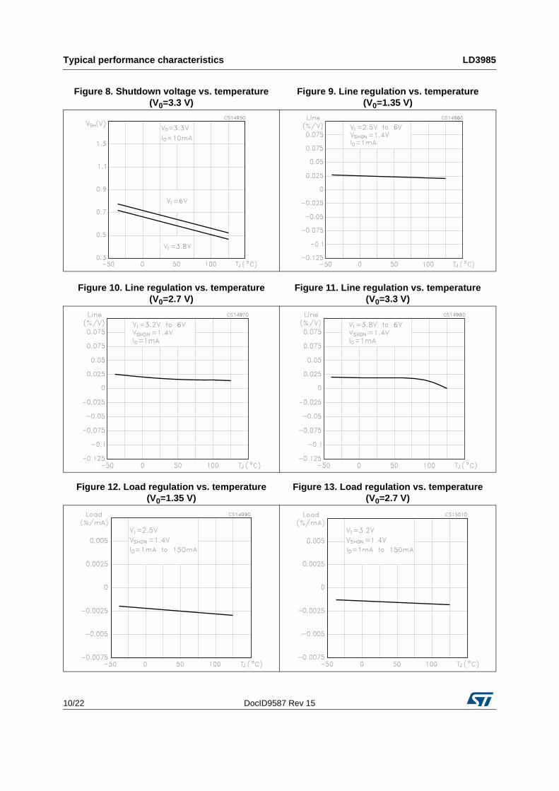
Typical performance characteristics LD3985
10/22 DocID9587 Rev 15
Figure 8. Shutdown voltage vs. temperature (V0=3.3 V)
Figure 9. Line regulation vs. temperature (V0=1.35 V)
Figure 10. Line regulation vs. temperature (V0=2.7 V)
Figure 11. Line regulation vs. temperature (V0=3.3 V)
Figure 12. Load regulation vs. temperature (V0=1.35 V)
Figure 13. Load regulation vs. temperature (V0=2.7 V)
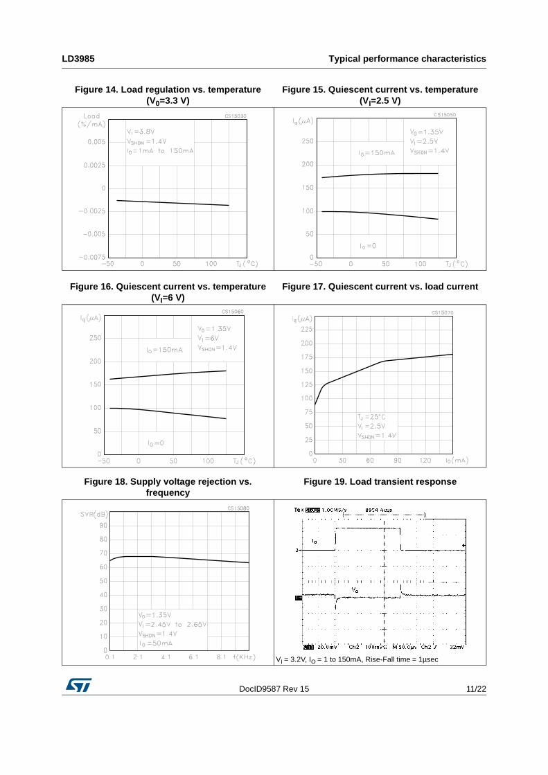
DocID9587 Rev 15 11/22
LD3985 Typical performance characteristics
22
Figure 14. Load regulation vs. temperature (V0=3.3 V)
Figure 15. Quiescent current vs. temperature (VI=2.5 V)
Figure 16. Quiescent current vs. temperature (VI=6 V)
Figure 17. Quiescent current vs. load current
Figure 18. Supply voltage rejection vs. frequency
Figure 19. Load transient response
VI = 3.2V, IO = 1 to 150mA, Rise-Fall time = 1µsec
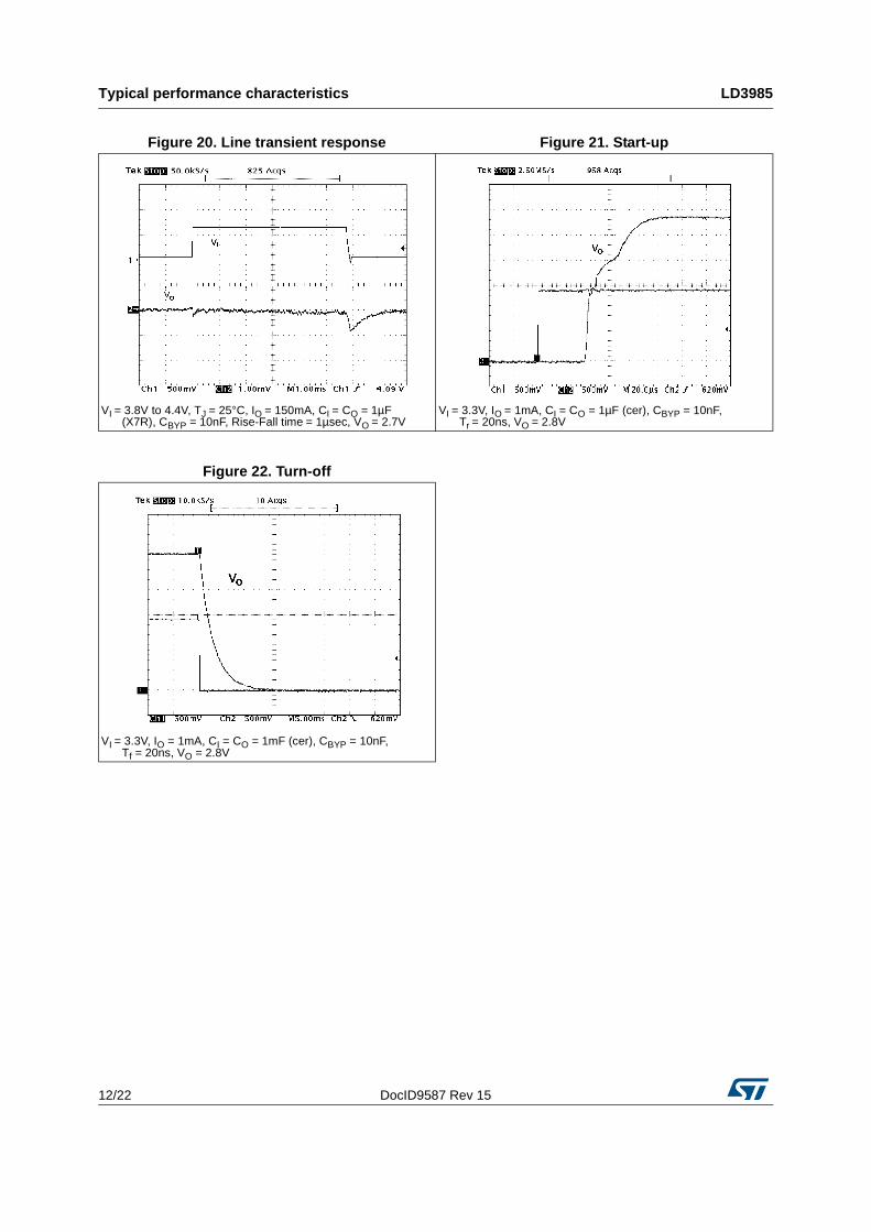
Typical performance characteristics LD3985
12/22 DocID9587 Rev 15
Figure 20. Line transient response Figure 21. Start-up
VI = 3.8V to 4.4V, TJ = 25°C, IO = 150mA, CI = CO = 1µF (X7R), CBYP = 10nF, Rise-Fall time = 1µsec, VO = 2.7V
VI = 3.3V, IO = 1mA, CI = CO = 1µF (cer), CBYP = 10nF, Tr = 20ns, VO = 2.8V
Figure 22. Turn-off
VI = 3.3V, IO = 1mA, CI = CO = 1mF (cer), CBYP = 10nF, Tf = 20ns, VO = 2.8V
DocID9587 Rev 15 13/22
LD3985 Package mechanical data
22
7 Package mechanical data
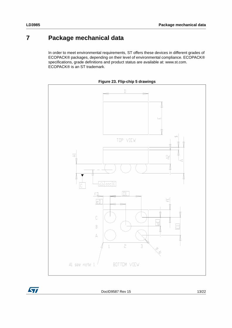
In order to meet environmental requirements, ST offers these devices in different grades of ECOPACK® packages, depending on their level of environmental compliance. ECOPACK® specifications, grade definitions and product status are available at: www.st.com. ECOPACK® is an ST trademark.
Figure 23. Flip-chip 5 drawings
Package mechanical data LD3985
14/22 DocID9587 Rev 15
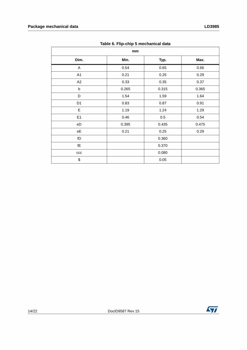
Table 6. Flip-chip 5 mechanical data
mm
Dim. Min. Typ. Max.
A 0.54 0.65 0.66
A1 0.21 0.25 0.29
A2 0.33 0.35 0.37
b 0.265 0.315 0.365
D 1.54 1.59 1.64
D1 0.83 0.87 0.91
E 1.19 1.24 1.29
E1 0.46 0.5 0.54
eD 0.395 0.435 0.475
eE 0.21 0.25 0.29
fD 0.360
fE 0.370
ccc 0.080
$ 0.05
DocID9587 Rev 15 15/22
LD3985 Package mechanical data
22
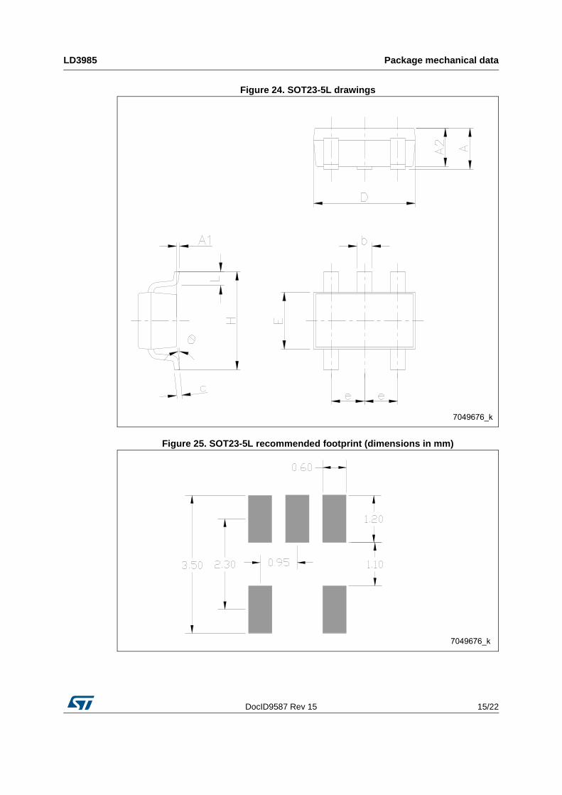
Figure 24. SOT23-5L drawings
Figure 25. SOT23-5L recommended footprint (dimensions in mm)
Package mechanical data LD3985
16/22 DocID9587 Rev 15
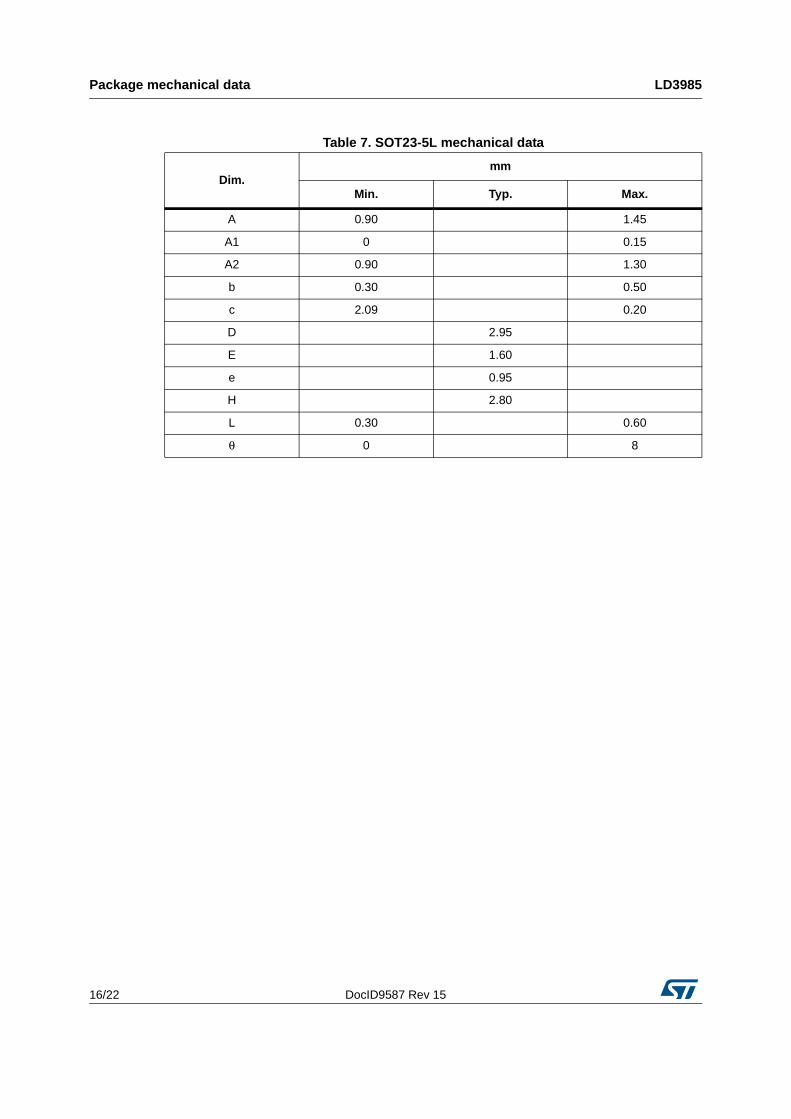
Table 7. SOT23-5L mechanical data
Dim.mm
Min. Typ. Max.
A 0.90 1.45
A1 0 0.15
A2 0.90 1.30
b 0.30 0.50
c 2.09 0.20
D 2.95
E 1.60
e 0.95
H 2.80
L 0.30 0.60
θ 0 8
DocID9587 Rev 15 17/22
LD3985 Package mechanical data
22
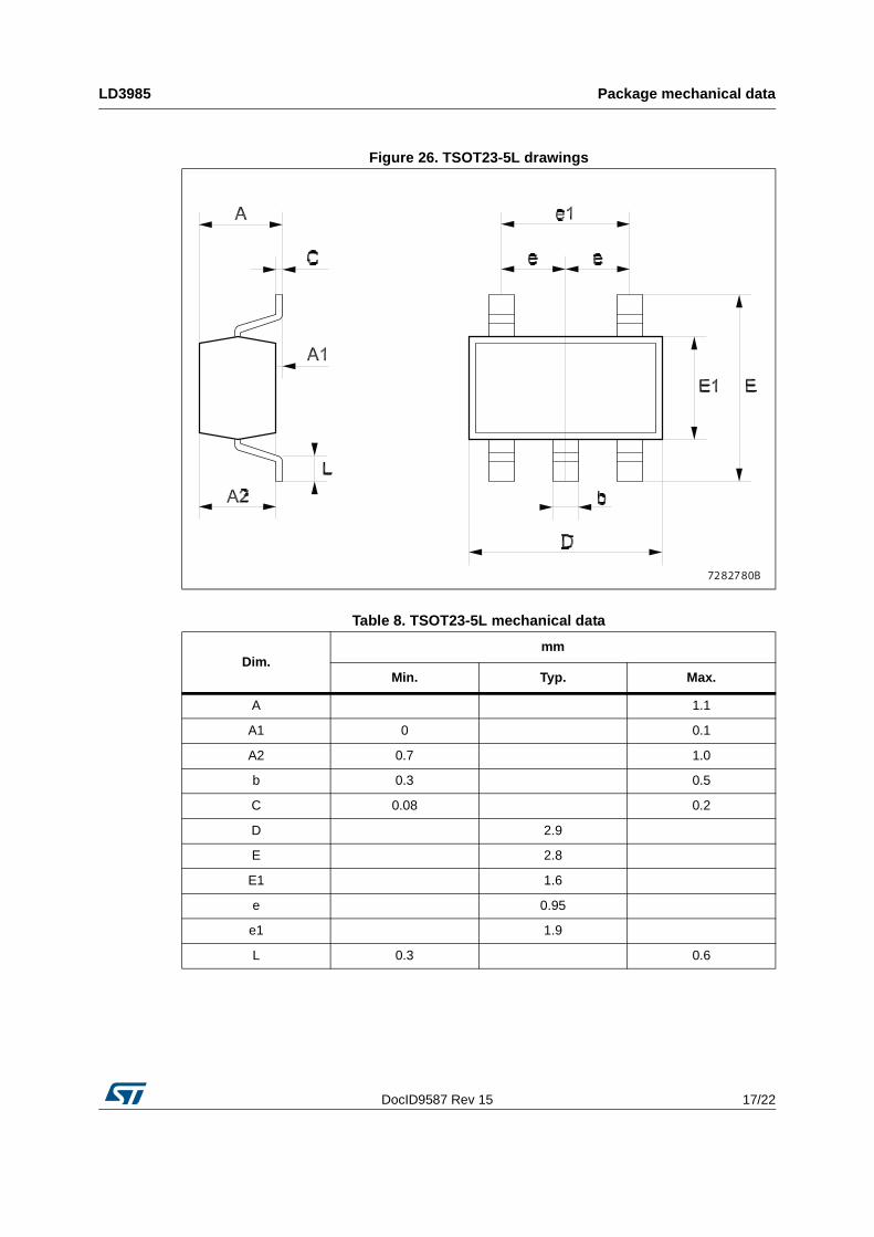
Figure 26. TSOT23-5L drawings
Table 8. TSOT23-5L mechanical data
Dim.mm
Min. Typ. Max.
A 1.1
A1 0 0.1
A2 0.7 1.0
b 0.3 0.5
C 0.08 0.2
D 2.9
E 2.8
E1 1.6
e 0.95
e1 1.9
L 0.3 0.6
7282780B
Packaging mechanical data LD3985
18/22 DocID9587 Rev 15
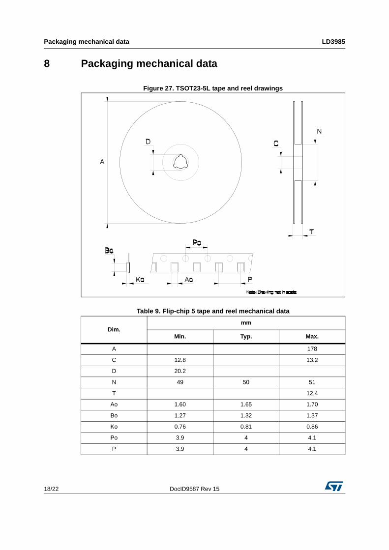
8 Packaging mechanical data
Figure 27. TSOT23-5L tape and reel drawings
Table 9. Flip-chip 5 tape and reel mechanical data
Dim.mm
Min. Typ. Max.
A 178
C 12.8 13.2
D 20.2
N 49 50 51
T 12.4
Ao 1.60 1.65 1.70
Bo 1.27 1.32 1.37
Ko 0.76 0.81 0.86
Po 3.9 4 4.1
P 3.9 4 4.1
DocID9587 Rev 15 19/22
LD3985 Packaging mechanical data
22
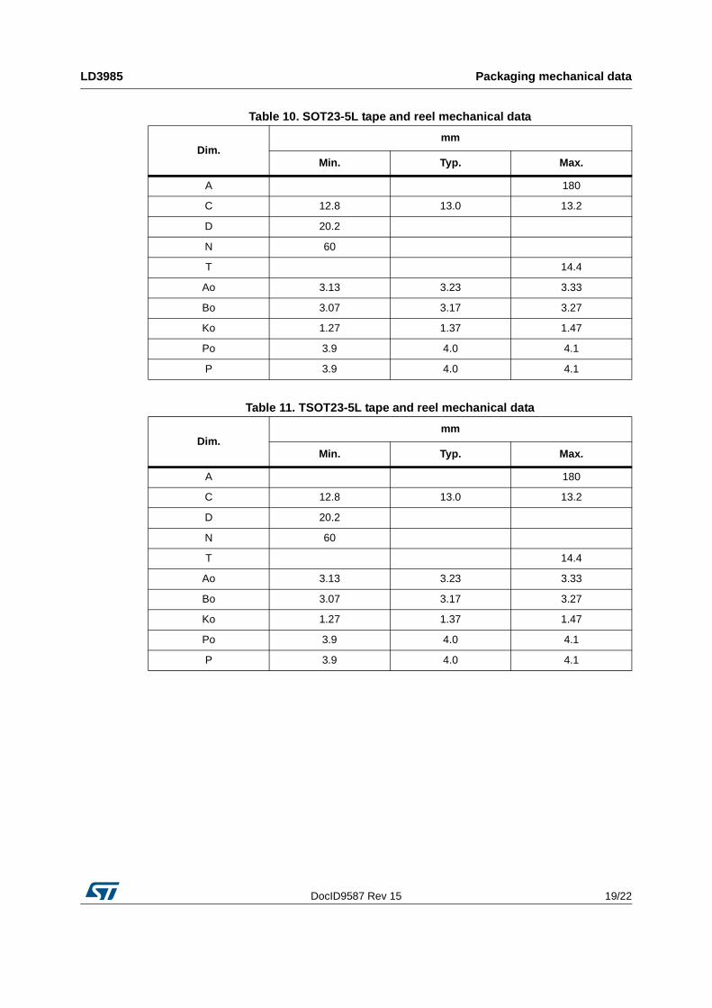
Table 10. SOT23-5L tape and reel mechanical data
Dim.mm
Min. Typ. Max.
A 180
C 12.8 13.0 13.2
D 20.2
N 60
T 14.4
Ao 3.13 3.23 3.33
Bo 3.07 3.17 3.27
Ko 1.27 1.37 1.47
Po 3.9 4.0 4.1
P 3.9 4.0 4.1
Table 11. TSOT23-5L tape and reel mechanical data
Dim.mm
Min. Typ. Max.
A 180
C 12.8 13.0 13.2
D 20.2
N 60
T 14.4
Ao 3.13 3.23 3.33
Bo 3.07 3.17 3.27
Ko 1.27 1.37 1.47
Po 3.9 4.0 4.1
P 3.9 4.0 4.1
Order codes LD3985
20/22 DocID9587 Rev 15
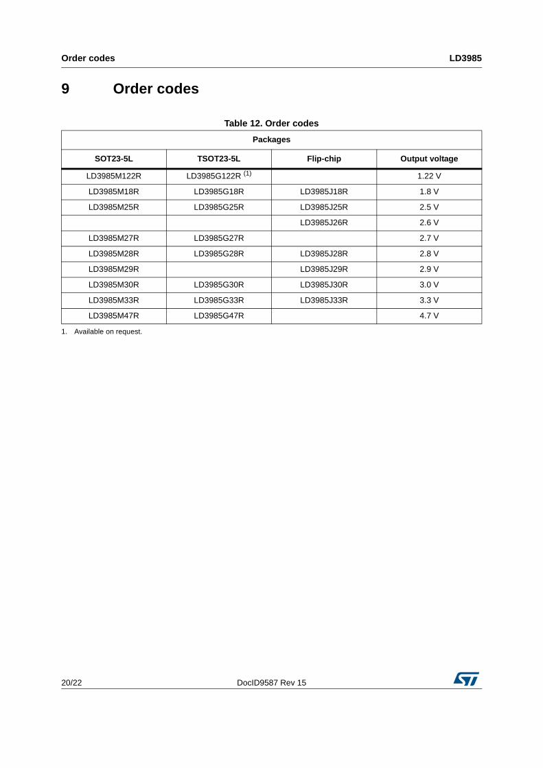
9 Order codes
Table 12. Order codes
Packages
SOT23-5L TSOT23-5L Flip-chip Output voltage
LD3985M122R LD3985G122R (1)
1. Available on request.
1.22 V
LD3985M18R LD3985G18R LD3985J18R 1.8 V
LD3985M25R LD3985G25R LD3985J25R 2.5 V
LD3985J26R 2.6 V
LD3985M27R LD3985G27R 2.7 V
LD3985M28R LD3985G28R LD3985J28R 2.8 V
LD3985M29R LD3985J29R 2.9 V
LD3985M30R LD3985G30R LD3985J30R 3.0 V
LD3985M33R LD3985G33R LD3985J33R 3.3 V
LD3985M47R LD3985G47R 4.7 V
DocID9587 Rev 15 21/22
LD3985 Revision history
22
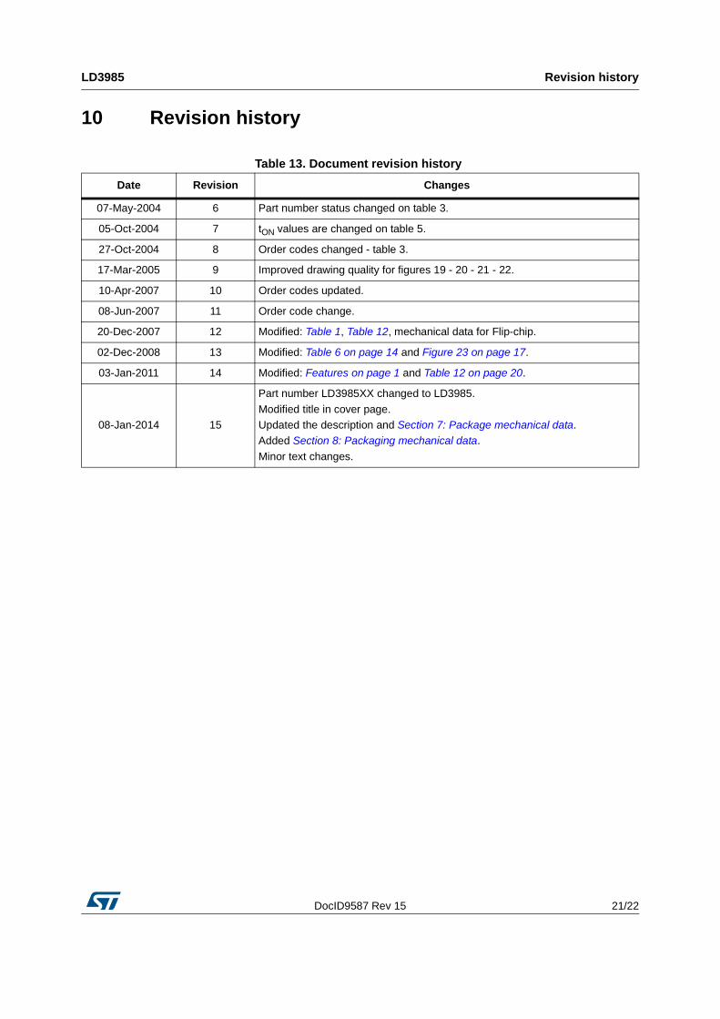
10 Revision history
Table 13. Document revision history
Date Revision Changes
07-May-2004 6 Part number status changed on table 3.
05-Oct-2004 7 tON values are changed on table 5.
27-Oct-2004 8 Order codes changed - table 3.
17-Mar-2005 9 Improved drawing quality for figures 19 - 20 - 21 - 22.
10-Apr-2007 10 Order codes updated.
08-Jun-2007 11 Order code change.
20-Dec-2007 12 Modified: Table 1, Table 12, mechanical data for Flip-chip.
02-Dec-2008 13 Modified: Table 6 on page 14 and Figure 23 on page 17.
03-Jan-2011 14 Modified: Features on page 1 and Table 12 on page 20.
08-Jan-2014 15
Part number LD3985XX changed to LD3985.
Modified title in cover page.Updated the description and Section 7: Package mechanical data.Added Section 8: Packaging mechanical data.
Minor text changes.
LD3985
22/22 DocID9587 Rev 15
Please Read Carefully:
Information in this document is provided solely in connection with ST products. STMicroelectronics NV and its subsidiaries (“ST”) reserve theright to make changes, corrections, modifications or improvements, to this document, and the products and services described herein at anytime, without notice.
All ST products are sold pursuant to ST’s terms and conditions of sale.
Purchasers are solely responsible for the choice, selection and use of the ST products and services described herein, and ST assumes noliability whatsoever relating to the choice, selection or use of the ST products and services described herein.
No license, express or implied, by estoppel or otherwise, to any intellectual property rights is granted under this document. If any part of thisdocument refers to any third party products or services it shall not be deemed a license grant by ST for the use of such third party productsor services, or any intellectual property contained therein or considered as a warranty covering the use in any manner whatsoever of suchthird party products or services or any intellectual property contained therein.
UNLESS OTHERWISE SET FORTH IN ST’S TERMS AND CONDITIONS OF SALE ST DISCLAIMS ANY EXPRESS OR IMPLIEDWARRANTY WITH RESPECT TO THE USE AND/OR SALE OF ST PRODUCTS INCLUDING WITHOUT LIMITATION IMPLIEDWARRANTIES OF MERCHANTABILITY, FITNESS FOR A PARTICULAR PURPOSE (AND THEIR EQUIVALENTS UNDER THE LAWSOF ANY JURISDICTION), OR INFRINGEMENT OF ANY PATENT, COPYRIGHT OR OTHER INTELLECTUAL PROPERTY RIGHT.
ST PRODUCTS ARE NOT DESIGNED OR AUTHORIZED FOR USE IN: (A) SAFETY CRITICAL APPLICATIONS SUCH AS LIFESUPPORTING, ACTIVE IMPLANTED DEVICES OR SYSTEMS WITH PRODUCT FUNCTIONAL SAFETY REQUIREMENTS; (B)AERONAUTIC APPLICATIONS; (C) AUTOMOTIVE APPLICATIONS OR ENVIRONMENTS, AND/OR (D) AEROSPACE APPLICATIONSOR ENVIRONMENTS. WHERE ST PRODUCTS ARE NOT DESIGNED FOR SUCH USE, THE PURCHASER SHALL USE PRODUCTS ATPURCHASER’S SOLE RISK, EVEN IF ST HAS BEEN INFORMED IN WRITING OF SUCH USAGE, UNLESS A PRODUCT ISEXPRESSLY DESIGNATED BY ST AS BEING INTENDED FOR “AUTOMOTIVE, AUTOMOTIVE SAFETY OR MEDICAL” INDUSTRYDOMAINS ACCORDING TO ST PRODUCT DESIGN SPECIFICATIONS. PRODUCTS FORMALLY ESCC, QML OR JAN QUALIFIED AREDEEMED SUITABLE FOR USE IN AEROSPACE BY THE CORRESPONDING GOVERNMENTAL AGENCY.
Resale of ST products with provisions different from the statements and/or technical features set forth in this document shall immediately voidany warranty granted by ST for the ST product or service described herein and shall not create or extend in any manner whatsoever, anyliability of ST.
ST and the ST logo are trademarks or registered trademarks of ST in various countries.Information in this document supersedes and replaces all information previously supplied.
The ST logo is a registered trademark of STMicroelectronics. All other names are the property of their respective owners.
© 2014 STMicroelectronics - All rights reserved
STMicroelectronics group of companies
Australia - Belgium - Brazil - Canada - China - Czech Republic - Finland - France - Germany - Hong Kong - India - Israel - Italy - Japan - Malaysia - Malta - Morocco - Philippines - Singapore - Spain - Sweden - Switzerland - United Kingdom - United States of America
www.st.com