Embed Size (px)
Citation preview
Ultra high resolution tomographic reconstruction using Focused Ion Beam (FIB) and Scanning Electron Microscope (SEM) Techniques
R. K. Bansal, R. Hull, and J. M. Fitz-Gerald University of Virginia, Charlottesville, Virginia 22904
AVS 51th International Symposium & Exhibition, November 14-19, 2004 Anaheim, CA
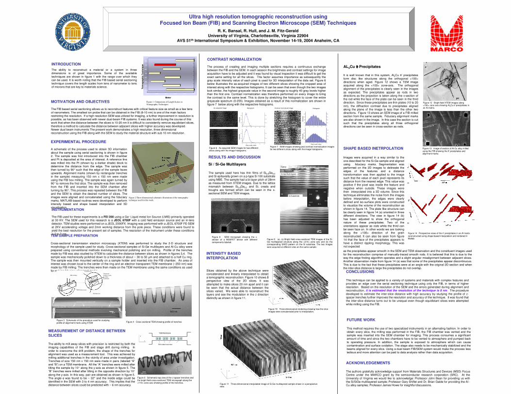
Figure 1 Comparison of Length Scales in Tomographic Techniques
1.0E-10 1.0E-08 1.0E-06 1.0E-04 1.0E-02 1.0E+00
X-Ray
SEM
TEM
PIXE
FIM
SIMS
FIB
MRI
Meter
Tom
ogra
phic
Tec
hniq
ueINTRODUCTIONThe ability to reconstruct a material or a system in three dimensions is of great importance. Some of the available techniques are shown in figure 1 with the range over which they can be used. It is worth noting that the FIB based serial sectioning technique covers the length scales from tens of nanometer to tens of microns that are key to materials science.
MOTIVATION AND OBJECTIVES
The FIB based serial sectioning allows us to reconstruct features with critical feature size as small as a few tens of nanometers. The smallest ion probe that can be obtained in the FIB (8-10 nm) is one of the main factors restricting the resolution. If a high resolution SEM was utilized for imaging, a further improvement in resolution is possible, as has been observed with newer dual-beam FIB systems. It was also found during the course of this work that when the distance between the slices is 10-20 nm it is difficult to consistently remove equidistant slices,therefore a method to calculate the distance between adjacent slices with higher accuracy was developed.Newer dual beam instruments The present work demonstrates a high resolution, three dimensional reconstruction using the FIB along with the SEM to study the material structure with sub 10 nm resolution.
EXPERIMENTAL PROCEDURE
A schematic of the process used to obtain 3D information about the sample using serial sectioning is shown in figure 2. The sample was first introduced into the FIB chamber and Pt is deposited at the area of interest. A reference line was milled into the Pt (shown by a darker shade) block to determine the distance from the edge. The sample was then turned by 90° such that the edge of the sample faces upwards. Alignment marks (shown by rectangular trenches in the sample) measuring 150 nm x 150 nm were made using the FIB box milling. The sample was again turned by 90° to remove the first slice. The sample was then removed from the FIB and inserted into the SEM chamber after turning by 90°. This process was repeated between the FIB and the SEM to obtain the desired number of slices. The images were aligned and concatenated using the fiduciary marks. MATLAB based routines were developed to perform intensity based and shape based interpolation and 3D visualization.
TEM SAMPLE PREPARATION
Cross-sectional transmission electron microscopy (XTEM) was performed to study the 2-D structure and morphology of the sample used for study. Cross-sectional samples of Si-Ge multilayers and Al-Cu alloy were prepared using conventional methods involving mechanical polishing and ion milling. Profile of the trenches made by FIB was also studied by XTEM to calculate the distance between slices as shown in figures 3,4. The sample was mechanically polished down to a thickness of about ~ 30 to 50 �m and attached to a half Cu ring. The sample was then mounted vertically on a sample holder and inserted into the FIB chamber. An area of interest was chosen local to the center of the ring and an electron transparent TEM membrane (~250 nm) was made by FIB milling. The trenches were then made on the TEM membrane using the same conditions as used for making fiduciary alignment marks.
INSTRUMENTATION
The FIB used for these experiments is a FEI 200 using a Ga+ Liquid metal Ion Source (LMIS) primarily operated at 30 KV. The SEM used for this research is a JEOL 6700F with a cold field emission source and an in-lens detector. TEM studies were performed on a JEOL 2000FX. Imaging was performed with a JEOL 6700F FE-SEM at 2KV accelerating voltage and 2mm working distance from the pole piece. These conditions were found to yield the best resolution for the present set of samples. The resolution of the instrument under these conditions is 2 to 3 nm
ACKNOWLEDGEMENTS
The authors gratefully acknowledge support from Materials Structures and Devices (MSD) Focus Centre under the MARCO grant by the semiconductor research corporation (SRC). At the University of Virginia we would like to acknowledge: Professor John Bean for providing us with the Si/SiGe multilayered sample; Professor Gary Shiflet and Dr. Brian Gable for providing the Al -Cu alloy samples; Professor James Howe for insightful discussions.
FUTURE WORK
This method requires the use of two specialized instruments in an alternating fashion. In order to obtain every slice, the milling was performed in the FIB, the FIB chamber was vented and the sample was inserted into the SEM chamber for imaging. This process consumes a significant amount of time and since the two chambers have to be vented to atmosphere and pumped back to operating pressure. In addition, the sample is exposed to atmosphere which can cause contamination and surface oxidation. The stage also needs to be mechanically stabilized and the beams aligned for every slice. Using a dual beam FIB/SEM system would make the process less tedious and more attention can be paid to data analysis rather than data acquisition.
CONCLUSIONS
This technique can be applied to a variety of systems and materials with complex features and provides an edge over the serial sectioning technique using only the FIB, in terms of higher resolution. Based on the resolution of the SEM and the errors generated during alignment and reconstruction, it is estimated that the resolution of the technique is 8 nm. The procedure developed to estimate the inter-slice distance with high accuracy by studying the profile of z-spacer trenches further improves the resolution and accuracy of the technique. It was found that the inter-slice distance turns out to be unequal even though equidistant slices were attempted while milling using the FIB.
MEASUREMENT OF DISTANCE BETWEEN SLICES
The ability to mill away slices with precision is restricted by both the imaging capabilities of the FIB and stage drift during milling. In order to overcome the drift problem, the shape of the trenches for alignment was used as a measurement tool. This was achieved by milling additional trenches in the vicinity of area under investigation. Trenches of size 150 nm x 150 nm were made in pairs (labeled “A”and “B”) on a TEM membrane. All the “A” trenches were milled after tilting the sample by 10° along the y-axis as shown in figure 5. The “B” trenches were milled after tilting in the opposite direction by 10°along the y-axis. In this way, pair are obtained as shown in figure 5. The angle φ was found to be ~ 32° and the inside edge could be identified in the SEM with 3 to 4 nm accuracy. This implies that the distance between slices could be predicted with ~ 6 nm accuracy.
Figure 4 Cross sectional TEM showing profile of trenches
500 nm
RESULTS AND DISCUSSION
Si / Si-Ge Multilayers
The sample used here has thin films of Si0.8Ge0.2and Si epitaxially grown on a p-type Si 100 substrate using MBE. The sample had a bi-layer pitch of 28nm as measured from XTEM images. Due to the lattice mismatch between Si0.8Ge0.2 and Si, crests and troughs are formed which can be seen in the x-sectional SEM and TEM images.
Figure 8 SEM micrograph showing the x-section of a MOSFET device with different components labeled.
Figure 2 Three-dimensional schematic illustration of the tomography technique used for this work.
FIB etching
TEM observation
Etching area
Etching area
Alignment trenches made on TEM membrane
1 ���� m
TEM membraneAlignment trenches made by FIB
Figure 3 Schematic of the procedure used for studying profile of alignment marls using XTEM
Figure 5 Schematic top view of the z-spacer trenches and the bright field cross-sectional TEM micrograph along the <110> zone axis showing profile of the trenches.
x
y
TEM Membrane
A B A B A B
FIB milled trenches
A B
φ°
200 nm
x
z
AA
AA
BB
BB
0 50 100 150 200 2500 0
1000 1000
2000 2000
0 50 100 150 200 2500 0
1000 1000
2000 2000
3000 3000
Gray scale value
Inte
nsity
Histogram
Figure 6 As acquired SEM images for two different slices along with the image histograms.
As-acquired image
Inte
nsity
Contrast normalized image Histogram
0 50 100 150 200 2500 0
1000 1000
2000 2000
3000 3000
4000 4000
0 50 100 150 200 2500 0
1000 1000
2000 2000
3000 3000
4000 4000
Gray scale value
Inte
nsity
Figure 7 SEM images showing post contrast normalization imagesfor two different slices along with the image histograms.
Inte
nsity
CONTRAST NORMALIZATION
The process of creating and imaging multiple sections requires a continuous exchange between the FIB and the SEM. In each session the brightness and contrast settings for image acquisition have to be adjusted and it was found by visual inspection it was difficult to get the exact same setting for all the slices. This factor assumes importance as subsequently the gray scale intensity value of each pixel is used for 3D interpolation of the data set. Figure 6 below illustrates the as-acquired images of two different slices showing the cropped area of interest along with the respective histograms. It can be seen that even though the two images look similar, the highest grayscale value in the second image is roughly 40 gray levels higher than the first one. Contrast normalization was therefore performed on every image to bring the contrast to the same level. This is done by stretching the histogram to cover the entire grayscale spectrum (0-255). Images obtained as a result of this normalization are shown in figure 7 below along with the respective histograms.
Alignment marks
(a)
Figure 9 (a), (c) Bright field cross-sectional TEM images of the Si-Ge multilayered structure along the <210> zone axis and (b) the corresponding SAED pattern on the Si substrate. The two images were acquired at different sites on the same sample.
Si Substrate
Si-Ge Multi-layers
Epoxy
(a)
(c)
(b)
000
004
00-4
-24-2
-242
2-4-2
2-42
Figure 10 Three-dimensional rendering showing how the slice images were concatenated prior to interpolation.
x
zy
Figure 11 Three-dimensional interpolated image of Si-Ge multilayered sample shown in a perspective view.
x
zy
INTENSITY BASED INTERPOLATION
Slices obtained by the above technique were concatenated and linearly interpolated to obtain a tomographic reconstruction. Figure 10 shows a perspective view of the 2D slices. It was attempted to make slices 20 nm apart and it can be seen that the actual distance between the slices varied. We were able to reconstruct the layers and see the modulation in the z direction distinctly as shown in figure 11.
AL2Cu θθθθ Precipitates
It is well known that in this system, Al2Cu θ’ precipitates form disc like structures along the orthogonal <100> directions when aged. Figure 12 shows a TEM image acquired along the <100> zone-axis. The orthogonal alignment of the precipitates is clearly seen in the images as expected. The precipitates appear as rods in two directions as the projection is taken along the x-section of the rod while the face of the plate can be seen in the third direction. Since these precipitates are thin plates (10 to 20 nm), the diffraction contrast due to precipitates aligned along the plane of the image is less than the other two directions. Figure 13 shows an SEM image of a FIB milled section from the same sample. Fiduciary alignment marks are also shown in the image. In this case the section is cut such that the precipitates along all three orthogonal directions can be seen in cross-section as rods.
Figure 12 Bright field XTEM images along <100> zone axis showing Al2Cu θ’ precipitates in an Al matrix.
Figure 13 image of section of Al-Cu alloy milled using the FIB showing the θ’ precipitates and alignment marks.
A
BC
Figure 14 Perspective views of the �’ precipitates in an Al matrix reconstructed using shape based interpolation and rendered in Matlab
(a)
(b)
SHAPE BASED INETRPOLATION
Images were acquired in a way similar to the one described for the Si-Ge sample and aligned using fiduciary marks. Segmentation was performed on the 2D images to delineate the edges of the features and a distance transformation was then applied to the image such that the value of each pixel represents its distance from the nearest edge. This value was positive if the pixel was inside the feature and negative when outside. These images were then interpolated into a 3D volume. Since this technique eliminates the noise from the images before interpolation, the edges were clearly defined and iso-surface plots were constructed to visualize the volume of the reconstruction as shown in figure 14. The plate like structure can be clearly seen in figure 14 (a) oriented in three different directions. The view in figure 14 (b) has been adjusted to show the orthogonal nature of these precipitates. Two of the orientations appear as rods while the third can be seen face on. In other words we are looking along the <100> direction of the grain reconstructed. It can also be seen from figure 14 that the face of the precipitates appears to have a distinct rippling morphology. This was not expected
as the precipitates appear smooth in the SEM and TEM observation and the constituent images used for the reconstruction comprise of manually-traced smooth rods. It is believed that this is due to the way the edge finding algorithm operates and a slight angular misalignment between adjacent slices.Another observation made from figure 14 (a) was that some of the precipitates appear discontinuous. This is due to the fact that these precipitates were at an angle with the original 2D section and when the inter-slice distance is large the precipitates do not overlap.


![11.[23 36]quadrature radon transform for smoother tomographic reconstruction](https://img.pdfslide.us/doc/110x75/54825b12b07959520c8b478b/1123-36quadrature-radon-transform-for-smoother-tomographic-reconstruction.jpg)