Embed Size (px)
Citation preview
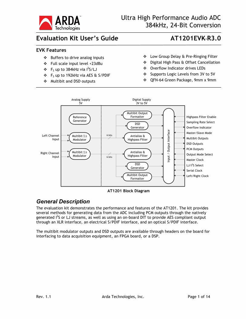
Ultra High Performance Audio ADC 384kHz, 24-Bit Conversion Evaluation Kit User’s Guide AT1201EVK–R3.0
Rev. 1.1 Arda Technologies, Inc. Page 1 of 14
EVK Features Buffers to drive analog inputs Full scale input level +23dBu FS up to 384kHz via I2S/LJ FS up to 192kHz via AES & S/PDIF Multibit and DSD outputs
Low Group Delay & Pre-Ringing Filter Digital High Pass & Offset Cancellation Overflow Indicator drives LEDs Supports Logic Levels from 3V to 5V QFN-64 Green Package, 9mm x 9mm
Multibit Σ∆ Modulator
DSD Generator
Antialias & Highpass Filter
Inpu
t /
Out
put
Inte
rfac
e
Left ChannelInput
Multibit Σ∆ Modulator
DSD Generator
Antialias & Highpass Filter
Right ChannelInput
Analog Supply5V
Digital Supply3V to 5V
PCM Outputs
DSD Outputs
Multibit Outputs6 bits
6 bits
Serial Clock
Left/Right Clock
Master/Slave Mode
Overflow Indicator
Sampling Rate Select
Highpass Filter Enable
Output Mode Select
LJ/I2S Select
Master Clock
Reference Generator
Multibit Output Formatter
Multibit Output Formatter
AT1201 Block Diagram
General Description The evaluation kit demonstrates the performance and features of the AT1201. The kit provides several methods for generating data from the ADC including PCM outputs through the natively generated I2S or LJ streams, as well as using an on-board DIT to provide AES compliant output through an XLR interface, an electrical S/PDIF interface, and an optical S/PDIF interface. The multibit modulator outputs and DSD outputs are available through headers on the board for interfacing to data acquisition equipment, an FPGA board, or a DSP.
Ultra High Performance Audio ADC 384kHz, 24-Bit Conversion Evaluation Kit User’s Guide AT1201EVK–R3.0
Rev. 1.1 Arda Technologies, Inc. Page 2 of 14
Testing the AT1201EVK This section describes the test setup for the evaluation board.
Items Needed 1. AT1201 Evaluation Board Rev. 3.0 2. Rohde & Schwarz UPV, Audio Precision SYS-2722 or equivalent Audio Analyzer 3. Power supplies for +6V and ±8V and power cables 4. Two XLR male to female cables to connect signal generators to the board 5. An XLR cable, an S/PDIF optical cable, an RCA cable, or a 10-pin header with a ribbon
cable to connect ADC outputs to the analyzer.
Audio Interfaces and Supported Sampling Rates Some audio interfaces have speed limitations that prevent them from supporting certain audio sampling rates. The following table shows the rates supported by each interface.
AES S/PDIF Optical
S/PDIF RCA
I2S
Single: 44.1/48 kHz Y Y Y Y Dual: 88.2/96 kHz Y Y Y Y Quad: 176.4/192 kHz Y Y Y Y Octal: 352.8/384 kHz N N N Y
Table 1: Sampling Rates Supported by Various Interface Standards
The I2S interface has been tested successfully at 384 kHz using a Rohde & Schwarz UPV with the optional I2S plug-in card.
Ultra High Performance Audio ADC 384kHz, 24-Bit Conversion Evaluation Kit User’s Guide AT1201EVK–R3.0
Rev. 1.1 Arda Technologies, Inc. Page 3 of 14
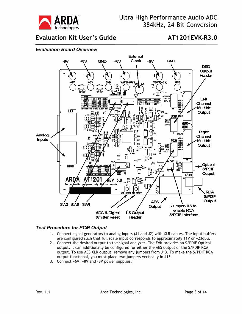
Evaluation Board Overview
Test Procedure for PCM Output 1. Connect signal generators to analog inputs (J1 and J2) with XLR cables. The input buffers
are configured such that full scale input corresponds to approximately 11V or +23dBu. 2. Connect the desired output to the signal analyzer. The EVK provides an S/PDIF Optical
output. It can additionally be configured for either the AES output or the S/PDIF RCA output. To use AES XLR output, remove any jumpers from J13. To make the S/PDIF RCA output functional, you must place two jumpers vertically in J13.
3. Connect +6V, +8V and -8V power supplies.
Ultra High Performance Audio ADC 384kHz, 24-Bit Conversion Evaluation Kit User’s Guide AT1201EVK–R3.0
Rev. 1.1 Arda Technologies, Inc. Page 4 of 14
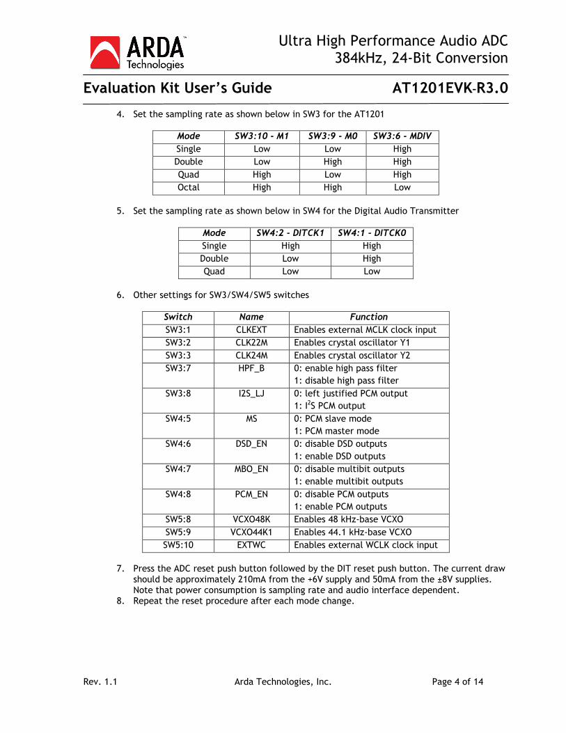
4. Set the sampling rate as shown below in SW3 for the AT1201
Mode SW3:10 - M1 SW3:9 - M0 SW3:6 - MDIV Single Low Low High Double Low High High Quad High Low High Octal High High Low
5. Set the sampling rate as shown below in SW4 for the Digital Audio Transmitter
Mode SW4:2 - DITCK1 SW4:1 - DITCK0 Single High High Double Low High Quad Low Low
6. Other settings for SW3/SW4/SW5 switches
Switch Name Function SW3:1 CLKEXT Enables external MCLK clock input SW3:2 CLK22M Enables crystal oscillator Y1 SW3:3 CLK24M Enables crystal oscillator Y2 SW3:7 HPF_B 0: enable high pass filter
1: disable high pass filter SW3:8 I2S_LJ 0: left justified PCM output
1: I2S PCM output SW4:5 MS 0: PCM slave mode
1: PCM master mode SW4:6 DSD_EN 0: disable DSD outputs
1: enable DSD outputs SW4:7 MBO_EN 0: disable multibit outputs
1: enable multibit outputs SW4:8 PCM_EN 0: disable PCM outputs
1: enable PCM outputs SW5:8 VCXO48K Enables 48 kHz-base VCXO SW5:9 VCXO44K1 Enables 44.1 kHz-base VCXO SW5:10 EXTWC Enables external WCLK clock input
7. Press the ADC reset push button followed by the DIT reset push button. The current draw
should be approximately 210mA from the +6V supply and 50mA from the ±8V supplies. Note that power consumption is sampling rate and audio interface dependent.
8. Repeat the reset procedure after each mode change.
Ultra High Performance Audio ADC 384kHz, 24-Bit Conversion Evaluation Kit User’s Guide AT1201EVK–R3.0
Rev. 1.1 Arda Technologies, Inc. Page 5 of 14
Clocking Modes The AT1201EVK supports several mechanisms for providing a master clock to the device under test: an external MCLK clock via BNC connector J7, on-board crystal oscillators Y1 and Y2, and an optional phase-locked loop, which may be specified at the time of ordering. Source selection is performed by using switches SW3:1..3 to select each of the MCLK sources, respectively. Note that only one of these switches should be in the HIGH position at any time, and SW5:10 should be in the LOW position as well. By default, the evaluation kit comes with a 24.576 MHz crystal oscillator in position Y2 and no PLL oscillator. The default 24.576 MHz crystal oscillator provides an on-board low jitter source for operating the AT1201 at 48 kHz, 96 kHz, 192 kHz, and 384 kHz PCM modes in addition to MBO and DSD modes. For clock rates at multiples of 44.1 kHz, an oscillator can be added at position Y1; this is also available upon request from Arda.
PLL configuration If your EVK is supplied with a phase-locked loop VCXO, it can be used by introducing a base-rate (PCM mode) clock at the BNC connector, choosing the desired VCXO at SW5:8 or 9, and enabling the external clock using SW5:10. The three MCLK sources at SW4 should be disabled, and only one VCXO should be enabled at a time. The clock supplied to the BNC input should be within approximately 200 ppm above or below the desired base rate, and the AT1201 must have PCM mode enabled (SW4:8 HIGH) and be in Master mode (SW4:5 HIGH) for the PLL to lock. DSD and MBO modes can also be used, though the MCLK is supplied by the EVK and locking to an external MCLK is not supported.
Overflow The overflow indicator output from the IC carries overflow information for both channels as a time multiplexed signal. The indicator drives an LED directly and is demuxed to drive two other LEDs representing each channel.
Buffer Gain & Bandwidth The analog input buffers, U2 and U3, have been designed for a 110 kHz -3dB, single pole roll-off. The buffer bandwidth can be altered by changing passives around the operational amplifiers. This is a complicated process that can have a significant impact on the performance of the DUT. Arda Technologies will provide assistance if a different bandwidth is desired. The signal gain through the input buffers is approximately 0.3 V/V, making the full-scale input level +23dBu. As with the buffer bandwidth, the gain can be altered by changing passives. Arda Technologies will provide assistance if a different gain is desired.
Digital Highpass Filter A first-order IIR highpass filter is present in the PCM signal path. The -3dB frequency is 0.47Hz at Fs = 48kHz and scales with Fs. The filter is activated using SW3:7. The highpass filter can be turned on for a few seconds to acquire the signal path offset and then disabled. Once disabled, the offset continues to be subtracted from the signal, but the filter’s frequency response is no longer present. Alternatively, the filter can be left enabled to operate continuously.
Ultra High Performance Audio ADC 384kHz, 24-Bit Conversion Evaluation Kit User’s Guide AT1201EVK–R3.0
Rev. 1.1 Arda Technologies, Inc. Page 6 of 14
Test Procedure for DSD and MBO Outputs Multibit and DSD outputs are available on the evaluation board. To activate these outputs, the MBO_EN or the DSD_EN signals must first be set high in SW4. The MBR5 .. MBR0 and MBL5 .. MBL0 outputs, corresponding to the right and left channels, respectively, begin to toggle when the MBO_EN signal is high. Bit 5 is the MSB, and bit 0 is the LSB. These logic signals must be clocked on the rising edge of the DCLK output from the DUT. The DSDR and DSDL outputs, corresponding to the right and left channels, respectively, are activated when the DSD_EN signal is high. They must be clocked on the rising edge of the DCLK output from the DUT.
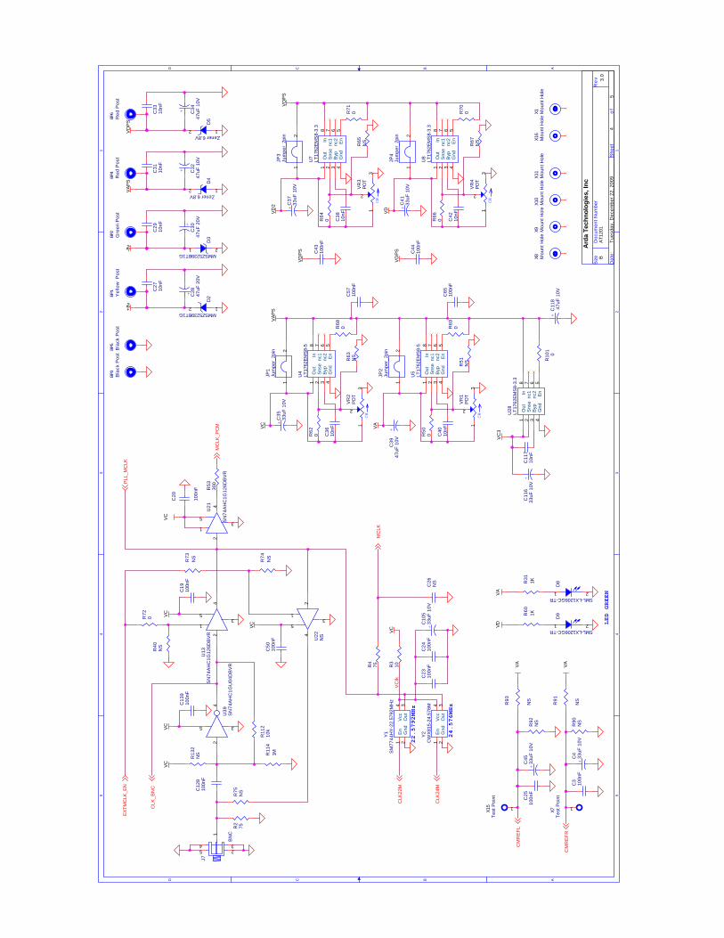
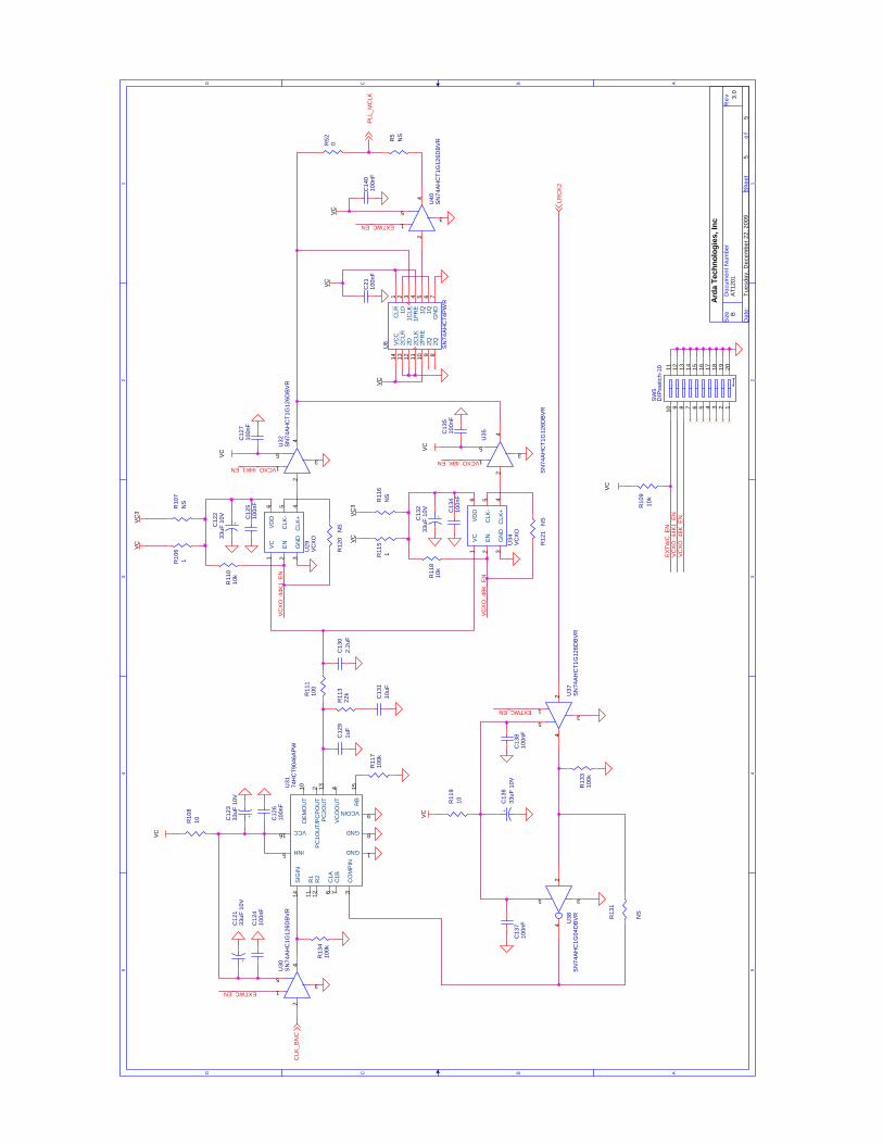
Board Schematics and Layout Evaluation board schematics are illustrated on the following pages. Gerber files for the board layout are available on request.
Contact Arda Technologies, Inc 148 Castro Street, Suite A1 Mountain View, CA 94041-1202 USA Tel: +1.650.961.9100 Fax: +1.650.961.9102 [email protected]
Ultra High Performance Audio ADC 384kHz, 24-Bit Conversion Evaluation Kit User’s Guide AT1201EVK–R3.0
Rev. 1.1 Arda Technologies, Inc. Page 7 of 14
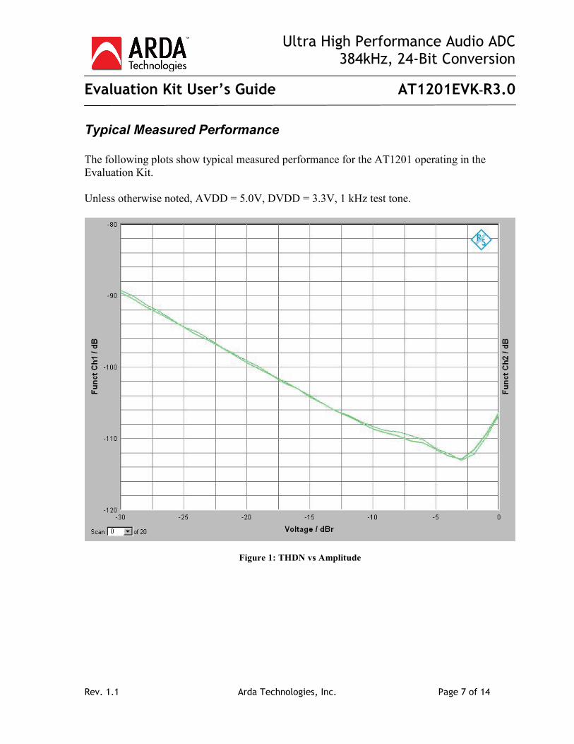
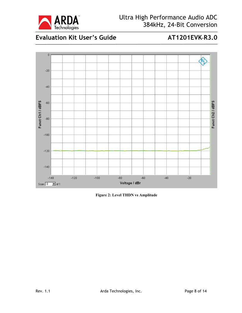
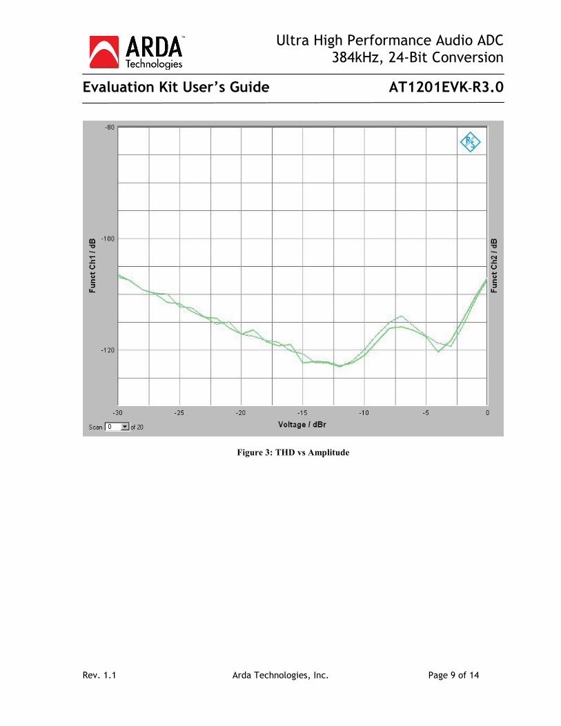
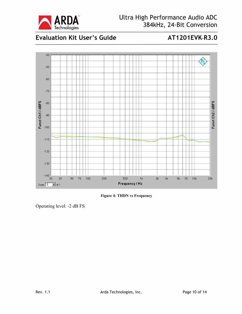
Typical Measured Performance The following plots show typical measured performance for the AT1201 operating in the Evaluation Kit. Unless otherwise noted, AVDD = 5.0V, DVDD = 3.3V, 1 kHz test tone.
Figure 1: THDN vs Amplitude
Ultra High Performance Audio ADC 384kHz, 24-Bit Conversion Evaluation Kit User’s Guide AT1201EVK–R3.0
Rev. 1.1 Arda Technologies, Inc. Page 8 of 14
Figure 2: Level THDN vs Amplitude
Ultra High Performance Audio ADC 384kHz, 24-Bit Conversion Evaluation Kit User’s Guide AT1201EVK–R3.0
Rev. 1.1 Arda Technologies, Inc. Page 9 of 14
Figure 3: THD vs Amplitude
Ultra High Performance Audio ADC 384kHz, 24-Bit Conversion Evaluation Kit User’s Guide AT1201EVK–R3.0
Rev. 1.1 Arda Technologies, Inc. Page 10 of 14
Figure 4: THDN vs Frequency Operating level: -2 dB FS
Ultra High Performance Audio ADC 384kHz, 24-Bit Conversion Evaluation Kit User’s Guide AT1201EVK–R3.0
Rev. 1.1 Arda Technologies, Inc. Page 11 of 14
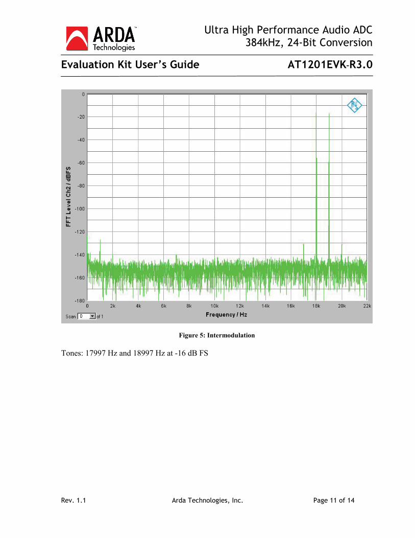
Figure 5: Intermodulation Tones: 17997 Hz and 18997 Hz at -16 dB FS
Ultra High Performance Audio ADC 384kHz, 24-Bit Conversion Evaluation Kit User’s Guide AT1201EVK–R3.0
Rev. 1.1 Arda Technologies, Inc. Page 12 of 14
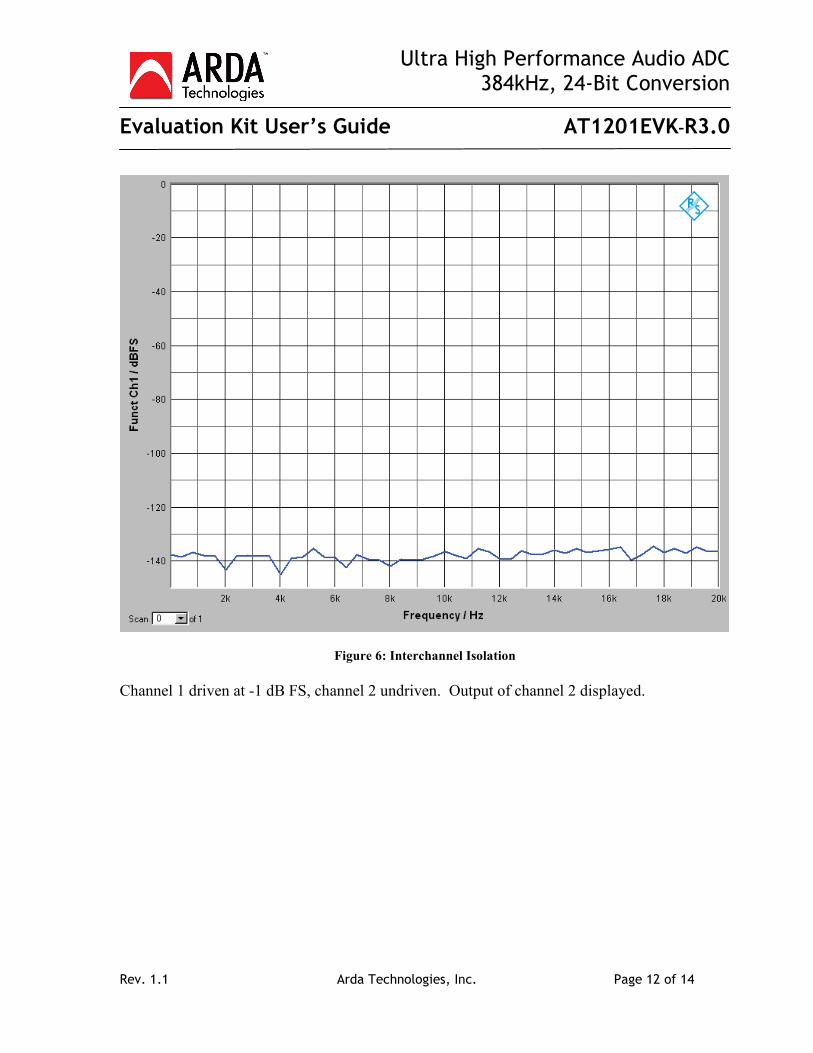
Figure 6: Interchannel Isolation Channel 1 driven at -1 dB FS, channel 2 undriven. Output of channel 2 displayed.
Ultra High Performance Audio ADC 384kHz, 24-Bit Conversion Evaluation Kit User’s Guide AT1201EVK–R3.0
Rev. 1.1 Arda Technologies, Inc. Page 13 of 14
EVALUATION BOARD LICENSE AGREEMENT BY USING THIS EVALUATION PRODUCT, YOU ARE AGREEING TO BE BOUND BY THE TERMS AND CONDITIONS OF THIS AGREEMENT. DO NOT USE THIS EVALUATION PRODUCT UNTIL YOU HAVE READ AND AGREED TO THE FOLLOWING TERMS AND CONDITIONS. IF YOU DO NOT AGREE WITH THEM, CONTACT THE ARDA TECHNOLOGIES WITHIN TEN (10) DAYS OF RECEIPT FOR INSTRUCTIONS ON RETURN OF THE UNUSED EVALUATION PRODUCT FOR A REFUND OF THE PURCHASE PRICE PAID. LICENSE. Arda Technologies, Inc. ("Arda") grants you the right to use the enclosed preproduction evaluation, demonstration, development, verification, or reference design board and/or kit, including any incorporated and/or accompanying software, components and documentation (collectively, the "Evaluation Product") solely for your evaluation, design and testing purposes. Certain software included with the Evaluation Product may be covered under a separate accompanying end user license agreement, in which case the terms and conditions of such end user license agreement shall apply to that software. PRE-PRODUCTION STATUS. The Evaluation Product is a pre-production product and has not been authorized under the rules of the United States Federal Communications Commission or the rules, regulations or laws of any country applicable to production systems or finished products for distribution to third parties. The Evaluation Product is not authorized for use in production systems, and may not be offered for sale or lease, or sold, leased or otherwise distributed. If the Evaluation Product is incorporated in a demonstration system, the demonstration system may be used by you solely for your evaluation, design and testing purposes. Such demonstration system may not be offered for sale or lease or sold, leased or otherwise distributed and must be accompanied by a conspicuous notice as follows: "This device is not, and may not be, offered for sale or lease, or sold or leased or otherwise distributed". OWNERSHIP AND COPYRIGHT. Title to the software, related documentation and all copies thereof remain with Arda and/or its licensors. You may not remove the copyright notices from the Evaluation Product. You agree to prevent any unauthorized copying of the Evaluation Product and related documentation. RESTRICTIONS. You may not sell or otherwise distribute the Evaluation Product for commercial purposes, in whole or in part, or use the Evaluation Product in production systems. Except as provided in this Agreement or in the Evaluation Product’s documentation, you may not reproduce the board or software or related documentation, or reverse engineer, de-compile or disassemble the software, in whole or in part. You agree that neither the Evaluation Product nor any other technical data received from Arda, nor the direct product thereof, will be directly or indirectly exported, re-exported or released to any destination or country for which the United States government or any agency thereof or other applicable non-U.S. governments or agencies, at the time of export, require an export license or other governmental approval, without first obtaining such license or approval. NO WARRANTY. The Evaluation Product is provided “as is” and “with all faults” without warranty of any kind. Arda and its licensors expressly disclaim all warranties, expressed, implied or otherwise, including without limitation, warranties of merchantability, fitness for a particular purpose and non-infringement of intellectual property rights. Arda and its licensors do not warrant that
Ultra High Performance Audio ADC 384kHz, 24-Bit Conversion Evaluation Kit User’s Guide AT1201EVK–R3.0
Rev. 1.1 Arda Technologies, Inc. Page 14 of 14
the evaluation product is compliant with European Union directives on the restriction of the use of certain hazardous substances in electrical and electronic equipment (ROHS) or waste electrical and electronic equipment (WEEE), that the evaluation product is production-worthy, that the functions contained in the Evaluation Product will meet your requirements, or that the operation of the Evaluation Product will be uninterrupted or error free. You are responsible for determining whether the Evaluation Product will be suitable for your intended use or application or will achieve your intended results. Prior to using or distributing any systems that have been evaluated, designed or tested using the Evaluation Product, you agree to thoroughly test and validate your design implementation to confirm the system functionality for your application. Arda has not authorized anyone to make any representation or warranty for the Evaluation Product, and any technical, applications or design information or advice, quality characterization, reliability data or other services provided by Arda shall not constitute any representation or warranty by Arda or alter this disclaimer of warranty, and no additional obligations or liabilities shall arise from Arda’s providing such information or services. Arda does not assume or authorize any other person to assume for it any other liability in connection with its Evaluation Products. LIMITATIONS OF LIABILITY. Arda or its licensors shall not be liable for any special, consequential, incidental, indirect or punitive damages, including but not limited to, the costs of labor, requalification, delay, loss of profits or goodwill, whether arising out of Arda’s performance or non-performance of this agreement or the use or inability to use the Evaluation Product, even if Arda is advised of the possibility of such damages. In no event shall Arda’s aggregate liability from any obligation arising out of or in connection with the license or use of any Evaluation Product provided hereunder, under any theory of liability including but not limited to contract, tort or promissory fraud liability, exceed the purchase price paid for the evaluation product, if any. To the maximum extent permitted under law, the limitations in this paragraph shall apply even if any limited remedy specified under this Agreement is found to have failed of its essential purpose. TERMINATION. Arda may terminate this license at any time if you are in breach of any of its terms and conditions. Upon termination, you will immediately return the Evaluation Product and documentation to Arda. GOVERNING LAW. This Agreement shall be governed by the laws of Delaware, excluding its principles of conflict of laws and the United Nationals Convention on Contracts for the Sale of Goods. NO WAIVER. The waiver by either party of any breach of any provision of this Agreement shall not operate or be construed as a waiver of any other or a subsequent breach of the same or a different provision. SEVERABILITY. If any term of this Agreement becomes or is declared to be invalid, illegal or unenforceable in any respect by any court of competent jurisdiction, such condition shall not affect the validity or enforceability of any of the remaining terms which remain in full force and effect.
5 5
4 4
3 3
2 2
1 1
DD
CC
BB
AA
-8v
+8v
-8v
+8v
+8v
-8v
-8v
VA
-8v
+8v
-8v
-8v
-8v
-8v
VA
-8v
+8v
+8v
VA
VA
VA
VA
INR
N
INR
P
INLP
INLN
BU
FRE
F
Size
Doc
umen
t Num
ber
Rev
Dat
e:S
heet
of
B
15
Tues
day,
Dec
embe
r 22,
200
9
3.0
AT12
01
Arda
Tec
hnol
ogie
s, In
c
C63
100n
F
X14
Test
Poi
nt
1
R22
270
0.1
%
C12
010
0nF
R10
3N
S
C69
3.9n
F C
OG
X12
Test
Poi
nt
1
R12
2N
S
R12
8N
S
C64
100n
F
R10
2N
S
+ -VOC
M
PD
U2
OPA1632DGN
7
8 1245
3 69
C73
1.2n
F C
OG
C59
1.2n
F C
OG
C58
1.2n
F C
OG
R88
1
C47
100n
F
R13
3K3
C68
3.9n
F C
OG
R8
910
0.1
%
C51
3.9n
F C
OG
R45
NS
R18
910
0.1
%
R20
40.2
1%
X2 Test
Poi
nt
1
R94
1
R12
9N
S
C11
910
0nF
R16
100
R7
100
R96
1
X3 Test
Poi
nt
1
C76
100n
F
R12
3N
S
R10
4N
S
+C
7033
uF 1
0V
R9
910
0.1
%
R29
3.3k
1%
R46
NS
+
C66
47uF
20V
R30
2.61
k 1%
R12
270
0.1
%
X4 Test
Poi
nt
1
R27
3K3
R21
40.2
1%
+C
5233
uF 1
0V
X6Te
st P
oint
1
C61
100n
F
-+
U20
BLM
4562
MA
5 67
8 4
R10
5N
S
R43
NS
C55
3.9n
F C
OG
C71
3.3n
F C
OG
X13
Test
Poi
nt
1
X5 Test
Poi
nt
1
R47
NS
R11
40.2
1%
R23
270
0.1
%
C62
100n
F
C54
100n
F
+C
7547
uF 2
0V+ -VO
CM
PD
U3
OPA1632DGN
7
8 1245
3 69
R19
910
0.1
%
+
C77
47uF
20V
R44
NS
+C
5347
uF 2
0V
C74
1.2n
F C
OG
J2X
LR-F
2
3
1
-+U20
ALM
4562
MA
3 21
8 4
C78
100n
F
+C
4833
uF 1
0V
R54
1K
R10
3K3
R28
3K3
C56
3.3n
F C
OG
R48
NS
R15
270
0.1
%
R14
40.2
1%
J1X
LR-F
2
3
1
PCB
PC
B1
PC
B-A
T120
1-13
R95
1
5 5
4 4
3 3
2 2
1 1
DD
CC
BB
AA
VD
2
VD
VD
2
VD
2
VD
2
VA
VD
VA
VD
VA
VD
VD
2
VD
VC
VD
VD
VD
2
VA
VA
-8v
+8v
+8v
-8v
-8v
+8v
+8v
-8v
VD
2
MBO
_En
MS
RS
TBS
CLK
LRC
K
SD
OU
T
INR
NIN
RP
BU
FRE
F
DIT
CK
1D
ITC
K0
EXTM
CLK
_EN
CLK
22M
CLK
24M
I2S
_LJ
MC
LK
OV
FLB
CM
RE
FR
MB
I_E
n
CM
RE
FL
INLP
INLN
U14
out
MC
LK_P
CM
2M
CLK
_PC
M
MB
I_E
n
MBO
_En
U14
out
U14
out
Size
Doc
umen
t Num
ber
Rev
Dat
e:S
heet
of
B
25
Tues
day,
Dec
embe
r 22,
200
9
3.0
AT12
01
Arda
Tec
hnol
ogie
s, In
c
R97
100
+
C10
847
uF 2
0V
1
2 3
4
5
6 7
8
9 1
011
12
13 1
415
16
17 1
819
20
J12
Hea
der_
2x10
pin
22
55
66
77
88
99
1010
11
44
33
1111
1212
1313
1414
1515
1616
1717
1818
1919
2020
C13
100n
F
RA
1010
0x4
Arr
ay1 2 3 4
5678
C10
100n
FC
910
0nF
RA
17
300x
4 A
rray
1 2 3 45678
1
2 3
4
5
6 7
8
9 1
0
J5 Hea
der_
2x5p
in
22
55
66
77
88
99
1010
11
44
33
R77
NS
C8
100n
FR
A4
10K
x4 A
rray1 2 3 4
5678
+
C96
33uF
10V
PO
LYM
ER
C11
310
0nF
-+
U25
BLM
4562
MA
5 67
8 4
+
C49
1500
uF 6
.3V
C7
100n
F
+C
106
47uF
20V
R99
100
RA
810
0x4
Arr
ay
1 2 3 45678
R12
50
U10
SN
74A
HC
245P
WR
A2
3B
217
Vcc
20
A3
4
Dir
1O
E19
A1
2B
118
A4
5A
56
A6
7A
78
A8
9G
nd10
B8
11B
712
B3
16B
415
B5
14B
613
C16
100n
F
U1
AT12
01
RS
TB35
DG
ND
37
MB
R0
40
DV
DD
36
LRC
K33
MB
R1
39
SC
LK34
MB
R2
38
DC
LK41
DS
DR
42D
SD
L43
DV
DD
44D
GN
D45
SD
OU
T46
MB
L047
MB
L148
MBL249 MBL350 MBL451 MBL552 MDIV53 HPFB54 DVDD55 DGND56 I2S_LJ57 M058 M159 OVFLB60 MCLK61 AGND62 AGND63 AGND64
RE
FNL
2
AG
ND
4IN
LP5
INLN
6A
GN
D7
AV
DD
8A
VD
D9
AG
ND
10IN
RN
11IN
RP
12A
GN
D13
CM
RE
FR14
RE
FNR
15R
EFP
R16
RE
FPL
1
BUFREF 17AGND 18AGND 19PCM_EN 20DGND 21DGND 22DGND 23DGND 24DVDD 25DGND 26MBO_EN 27DSD_EN 28MS 29MBR5 30MBR4 31MBR3 32
GND 65
CM
RE
FL3
RA
18
300x
4 A
rray
1 2 3 45678
RA
1610
Kx4
Arr
ay
12345
678
R12
40
-+
U26
BLM
4562
MA
5 67
8 4
R80 0
+
C11
447
uF 2
0V
+C
647
uF 1
0V
R81
NS
+C
111
33uF
10V
SW
4
DIP
switc
h-10
1 2 3 4 8765 9 1011121314151617181920
C10
910
0nF
1
2 3
4
5
6 7
8
9 1
011
12
13 1
415
16
17 1
819
20
J11
Hea
der_
2x10
pin
22
55
66
77
88
99
1010
11
44
33
1111
1212
1313
1414
1515
1616
1717
1818
1919
2020
+
C2
33uF
10V
PO
LYM
ER
+C
547
uF 1
0V
C95
47pF
R82
NS
RA
6
300x
4 A
rray
1 2 3 45678
+C
112
47uF
20V
RA
9
300x
4 A
rray
1 2 3 45678
C14
100n
F
C11
100n
F
R83
0-+
U26
ALM
4562
MA
3 21
8 4
+C
110
33uF
10V
U12
SN
74A
HC
245P
WR
A2
3B
217
Vcc
20
A3
4
Dir
1O
E19
A1
2B
118
A4
5A
56
A6
7A
78
A8
9G
nd10
B8
11B
712
B3
16B
415
B5
14B
613
+
C46
1500
uF 6
.3V
RA
19
100x
4 A
rray
1 2 3 45678
D1
SML-
LX12
06IC
-TR
12
R98
1
C10
710
0nF
SW
3
DIP
switc
h-10
1 2 3 4 8765 9 1011121314151617181920
C15
100n
F
U9
SN
74A
HC
245P
WR
A2
3B
217
Vcc
20
A3
4
Dir
1O
E19
A1
2B
118
A4
5A
56
A6
7A
78
A8
9G
nd10
B8
11B
712
B3
16B
415
B5
14B
613
-+
U25
ALM
4562
MA
3 21
8 4R
760
R10
01
R1
1K
RA
3
10K
x4 A
rray1 2 3 4
5678
C11
510
0nF
RA
5
300x
4 A
rray
1 2 3 45678
RA
20
100x
4 A
rray
1 2 3 45678
U14
SN
74A
HC
1G04
DB
VR
5 3
24
RA
1510
Kx4
Arr
ay
12345
678
RA
710
0x4
Arr
ay
1 2 3 45678
C1
47pF
5 5
4 4
3 3
2 2
1 1
DD
CC
BB
AA
VIO
VD
2
VD
2
VD
2
VD
VD
VA
PS
VD
2
VD
2
VD
2
VD
2
VD
2
VD
2
VD
2
VD
2
VD
2
VIO
VD
VIO
RS
TB
MC
LK_P
CM
2
MS
SD
OU
TLR
CK
SC
LK
OV
FLB
LRC
K2
DIT
CK
1D
ITC
K0
I2S
_LJ
LRC
K2
Size
Doc
umen
t Num
ber
Rev
Dat
e:S
heet
of
B
35
Tues
day,
Dec
embe
r 22,
200
9
3.0
AT12
01
PCM
Port
Overflow
Arda
Tec
hnol
ogie
s, In
c
Dual Footprint
U16
LT17
62EM
S8-
5#P
BF
Byp
3E
n5
In8
Gnd
4
Out
1nc
17
Sns
e2
nc2
6
U19
DIT
4192
IPW
L3
CLK
05
DG
ND
8
CLK
14
CS
S1
VIO
7
CO
PY
/C2
MC
LK6
FMT0
9FM
T110
SC
LK11
SY
NC
12S
DA
TA13
M/S
14R
ST
15D
GN
D16
TX-
17TX
+18
VD
D19
MD
AT
20M
ON
O21
AU
DIO
22E
MP
H23
BLS
M24
BLS
25V
26U
27M
OD
E28
+C
100
47uF
10V R
5636
0
J8 Aud
io R
CA
Jac
k
1
2
R86
0 C86
100n
F
1
2 3
4
5
6 7
8
9 1
0
J6 Hea
der_
2x5p
in
22
55
66
77
88
99
1010
11
44
33
C10
422
pF
R58
NS
C93
100n
F
R25
10k
J13
Hea
der_
2x2p
in
22
11
44
33
R17
1K
SW
2S
witc
h B
utto
n 31 2
4
R57
90.9
C17
100n
F
R61
0
J3XL
R-M 1
3
2
U11
SN
74A
HC
245P
WR
A2
3B
217
Vcc
20
A3
4
Dir
1O
E19
A1
2B
118
A4
5A
56
A6
7A
78
A8
9G
nd10
B8
11B
712
B3
16B
415
B5
14B
613
C80
100n
F
+C
8333
uF 1
0V
D6
SML-LX1206IC-TR
12
C90
10nF
C10
110
0nF
U17
SN
74A
HC
14P
WR
VC
C14
GN
D7
1Y2
2Y4
3Y6
4Y8
1A1
2A3
3A5
4A9
5A11
6A13
6Y12
5Y10
R26
10k
+C
8433
uF 1
0V
T1 602-
3724
61
8
6
45
2
73
C85
100n
F
C10
210
0nF
U18
SN
74A
HC
245P
WR
A2
3B
217
Vcc
20
A3
4
Dir
1O
E19
A1
2B
118
A4
5A
56
A6
7A
78
A8
9G
nd10
B8
11B
712
B3
16B
415
B5
14B
613
R24
110
R13
510
0
RA
2110
0x4
Arr
ay
1 2 3 45678
U23
SN
74A
HC
74P
WR
1CLK
31P
RE
4
CLR
11D
2
1Q5
1Q6
GN
D7
2Q8
2Q9
2PR
E10
2CLK
112D
12
VC
C14
2CLR
13
U15
SN
74A
HC
1G12
6DB
VR
53
24
1
C82
100n
F
SW
1S
witc
h B
utto
n 31 2
4
R55
150
R89
100
R6
1K
RA
2210
0x4
Arr
ay1 2 3 4
5678
C92
10nF
D7
SML-LX1206IC-TR12
J9 Con
n_Fi
berO
ptic
Vcc
2V
in1
GN
D3
RA
1310
0x4
Arr
ay
12345
678
C88
10nF
R13
00
U24
SN
74A
HC
1G04
DB
VR
5 3
24
U27
SN
74A
HC
1G04
DB
VR
5 3
24
JP5
Jum
per_
2pin 2
1
RA
1130
0x4
Arr
ay1 2 3 4
5678
RA
1210
0x4
Arr
ay1 2 3 4
5678
+C
7933
uF 1
0V
R59
NS
R49
10
C89
100n
F
1
2 3
4
5
6 7
8
9 1
0
J10
Hea
der_
2x5p
in
22
55
66
77
88
99
1010
11
44
33
C10
310
0nF
R85
NS
C87
100n
F
R87
100
C18
100n
F
5 5
4 4
3 3
2 2
1 1
DD
CC
BB
AA
VC
lk
VC
VC
VC
+8v
-8v
VA
PS
VD
PS
VD
2
VD
VA
VD
VD
PS
VA
VA
VC
VA
VD
PS
VC
VA
PS
VD
PS
VC
3
VC
VC
MC
LK
CLK
22M
CLK
24M
CM
RE
FL
CM
RE
FR
PLL
_MC
LK
MC
LK_P
CM
EXTM
CLK
_EN
CLK
_BN
C
Size
Doc
umen
t Num
ber
Rev
Dat
e:S
heet
of
B
45
Tues
day,
Dec
embe
r 22,
200
9
3.0
AT12
01
Arda
Tec
hnol
ogie
s, In
c
22.5792MHz
24.576MHz
LED GREEN
BP1
Yel
low
Pos
tBP
5B
lack
Pos
t
R63
NS
+
C28
47uF
20V
C29
10nF
C57
100n
F
U21
SN
74A
HC
1G12
6DB
VR
53
24
1
X1 Mou
nt H
ole
JP4
Jum
per_
2pin 2
1
C19
100n
F
U28
LT17
62EM
S8-
3.3
Byp
3E
n5
In8
Gnd
4
Out
1nc
17
Sns
e2
nc2
6
BP3
Bla
ck P
ost
+C
4133
uF 1
0V
U22
NS
53
24
1
CW
VR
1PO
T1
3
2
R13
2N
S
R31
1K
R70
0
R53
300
R4
75
C50
100n
F
U4
LT17
62EM
S8-5
Byp
3E
n5
In8
Gnd
4
Out
1nc
17
Sns
e2
nc2
6
R65
NS
R75
NS
C33
10nF
R50
0
+
C34
47uF
10V
C42
10nF
R60
1KR
92N
S
U8
LT17
62EM
S8-
3.3
Byp
3E
n5
In8
Gnd
4
Out
1nc
17
Sns
e2
nc2
6
+C
4533
uF 1
0V
C12
810
0nF
U7
LT17
62EM
S8-
3.3
Byp
3E
n5
In8
Gnd
4
Out
1nc
17
Sns
e2
nc2
6
BP4
Red
Pos
t
D5
Zener 6.8V2 1
R91
NS
R72
0
C43
100n
F
C65
100n
F
CW
VR
4PO
T1
3
2
+C
105
33uF
10V
C13
910
0nF
JP1
Jum
per_
2pin 2
1
J7
BN
C
2
1
54 3
R10
10
JP3
Jum
per_
2pin 2
1
R66
0
C25
100n
F
C23
100n
F
+C
3947
uF 1
0V
D9
SML-LX1206GC-TR1 2
R40
NS
C36
10nF
C24
100n
F
+
C32
47uF
10V
R11
210
k
+C
3733
uF 1
0V
R68
0
R73
NS
R90
NS
+C
3533
uF 1
0V
CW
VR
2PO
T1
3
2
C38
10nF
+
C30
47uF
20V
BP6
Red
Pos
t
R93
NS
R69
0
C40
10nF
U39
SN
74A
HC
1GU
04D
BV
R
5 32
4
BP2
Gre
en P
ost
U13
SN
74A
HC
1G12
6DB
VR
53
24
1
X7Te
st P
oint
1
X15
Test
Poi
nt
1
X11
Mou
nt H
ole
R62
0
R11
41M
R64
0
C11
710
nFX1
0M
ount
Hol
e
JP2
Jum
per_
2pin 2
1
C31
10nF
R71
0
R67
NS
Y1
SM
7744
HY
-22.
5792
MH
z
Gnd
2O
ut3
Vcc
4E
n1
D2
MMSZ5239BT1G2 1
X9 Mou
nt H
ole
+C
433
uF 1
0V
X16
Mou
nt H
ole
C27
10nF
R74
NS
D3
MMSZ5239BT1G21
CW
VR
3PO
T1
3
2
C3
100n
F
+C
118
47uF
10V
Y2
CW
X815
-24.
576M
Gnd
2O
ut3
Vcc
4E
n1
X8 Mou
nt H
ole
D4
Zener 6.8V2 1
D8
SML-LX1206GC-TR1 2
U5
LT17
62EM
S8-5
Byp
3E
n5
In8
Gnd
4
Out
1nc
17
Sns
e2
nc2
6
R3
10
C44
100n
F
C20
100n
F
R51
NS
C26
NS
+C
116
33uF
10V
R2
75
5 5
4 4
3 3
2 2
1 1
DD
CC
BB
AA
EXTWC_EN
EXTWC_EN
VCXO_44K1_ENVCXO_48K_EN
VC
XO
_44K
1_E
NV
CX
O_4
8K_E
N
VC
XO
_48K
_EN
VC
XO
_44K
1_E
N
EXTW
C_E
N
EXTWC_EN
VC
VC
VC
3
VC
VC
VC
3
VC
VC
VC
VC
VC
VC
PLL
_MC
LK
CLK
_BN
C
LRC
K2
Size
Doc
umen
t Num
ber
Rev
Dat
e:S
heet
of
B
55
Tues
day,
Dec
embe
r 22,
200
9
3.0
AT12
01
Arda
Tec
hnol
ogie
s, In
c
C12
710
0nF
R11
710
0k
C12
91u
F
C13
410
0nF
U40
SN
74A
HC
T1G
126D
BV
R
53
24
1
R11
810
k
+
C12
333
uF 1
0V
R10
910
k
+C12
233
uF 1
0VR
110
10k
C13
710
0nFC
124
100n
F
R13
410
0k
U35
SN
74A
HC
T1G
126D
BV
R
53
24
1
R12
0N
S
+C13
233
uF 1
0V
R10
810
R5
NS
+C
136
33uF
10V
R13
1
NS
R11
910
C21
100n
F
R10
61
R11
51
R11
110
0
R12
1N
S
C14
010
0nF
R11
322
k
SW
5D
IPsw
itch-
10
12348 7 6 591011 12 13 14 15 16 17 18 19 20
R52
0
R11
6N
S
U34
VCXO
VC
1
EN
2
GN
D3
CLK
+4
CLK
-5
VD
D6
U32
SN
74A
HC
T1G
126D
BV
R
53
24
1
U38
SN
74A
HC
1G04
DB
VR
5 3
24
U6
SN
74A
HC
74P
WR
1CLK
31P
RE
4
CLR
11D
2
1Q5
1Q6
GN
D7
2Q8
2Q9
2PR
E10
2CLK
112D
12
VC
C14
2CLR
13
C13
510
0nF
U37
SN
74A
HC
T1G
126D
BV
R
53
24
1
U29
VCXO
VC
1
EN
2
GN
D3
CLK
+4
CLK
-5
VD
D6
+
C12
133
uF 1
0V
C13
02.
2uF
C13
810
0nF
R10
7N
S
R13
310
0k
C12
610
0nF
U30
SN
74A
HC
1G12
6DB
VR
53
24
1
U31
74H
CT9
046A
PW
GND 1
VC
OO
UT
4C
1A6
C1B
7
GND 8D
EM
OU
T10
R1
11R
212
SIG
IN14
RB
15
VCC16
CO
MP
IN3
INH5
VCOIN 9
PC
1OU
T/P
CP
OU
T2
PC
2OU
T13
C13
110
uF
C12
510
0nF