Embed Size (px)
Citation preview

Order Number: 330236-002US
Intel® Quark™ SoC X1000UEFI Firmware Writer’s Guide
May 2014

Intel® Quark™ SoC X1000UEFI Firmware Writer’s Guide May 20142 Order Number: 330236-002US
Legal Lines and DisclaimersINFORMATION IN THIS DOCUMENT IS PROVIDED IN CONNECTION WITH INTEL PRODUCTS. NO LICENSE, EXPRESS OR IMPLIED, BY ESTOPPEL OR OTHERWISE, TO ANY INTELLECTUAL PROPERTY RIGHTS IS GRANTED BY THIS DOCUMENT. EXCEPT AS PROVIDED IN INTEL'S TERMS AND CONDITIONS OF SALE FOR SUCH PRODUCTS, INTEL ASSUMES NO LIABILITY WHATSOEVER AND INTEL DISCLAIMS ANY EXPRESS OR IMPLIED WARRANTY, RELATING TO SALE AND/OR USE OF INTEL PRODUCTS INCLUDING LIABILITY OR WARRANTIES RELATING TO FITNESS FOR A PARTICULAR PURPOSE, MERCHANTABILITY, OR INFRINGEMENT OF ANY PATENT, COPYRIGHT OR OTHER INTELLECTUAL PROPERTY RIGHT.A "Mission Critical Application" is any application in which failure of the Intel Product could result, directly or indirectly, in personal injury or death. SHOULD YOU PURCHASE OR USE INTEL'S PRODUCTS FOR ANY SUCH MISSION CRITICAL APPLICATION, YOU SHALL INDEMNIFY AND HOLD INTEL AND ITS SUBSIDIARIES, SUBCONTRACTORS AND AFFILIATES, AND THE DIRECTORS, OFFICERS, AND EMPLOYEES OF EACH, HARMLESS AGAINST ALL CLAIMS COSTS, DAMAGES, AND EXPENSES AND REASONABLE ATTORNEYS' FEES ARISING OUT OF, DIRECTLY OR INDIRECTLY, ANY CLAIM OF PRODUCT LIABILITY, PERSONAL INJURY, OR DEATH ARISING IN ANY WAY OUT OF SUCH MISSION CRITICAL APPLICATION, WHETHER OR NOT INTEL OR ITS SUBCONTRACTOR WAS NEGLIGENT IN THE DESIGN, MANUFACTURE, OR WARNING OF THE INTEL PRODUCT OR ANY OF ITS PARTS.Intel may make changes to specifications and product descriptions at any time, without notice. Designers must not rely on the absence or characteristics of any features or instructions marked "reserved" or "undefined". Intel reserves these for future definition and shall have no responsibility whatsoever for conflicts or incompatibilities arising from future changes to them. The information here is subject to change without notice. Do not finalize a design with this information.The products described in this document may contain design defects or errors known as errata which may cause the product to deviate from published specifications. Current characterized errata are available on request.Contact your local Intel sales office or your distributor to obtain the latest specifications and before placing your product order.Copies of documents which have an order number and are referenced in this document, or other Intel literature, may be obtained by calling 1-800-548-4725, or go to: http://www.intel.com/design/literature.htm Any software source code reprinted in this document is furnished for informational purposes only and may only be used or copied and no license, express or implied, by estoppel or otherwise, to any of the reprinted source code is granted by this document. Intel processor numbers are not a measure of performance. Processor numbers differentiate features within each processor family, not across different processor families. Go to: http://www.intel.com/products/processor_number/Code Names are only for use by Intel to identify products, platforms, programs, services, etc. (“products”) in development by Intel that have not been made commercially available to the public, i.e., announced, launched or shipped. They are never to be used as “commercial” names for products. Also, they are not intended to function as trademarks.Intel, the Intel logo, and Quark are trademarks of Intel Corporation in the U.S. and other countries.*Other names and brands may be claimed as the property of others.Copyright © 2014, Intel Corporation. All rights reserved.

Intel® Quark™ SoC X1000May 2014 UEFI Firmware Writer’s GuideOrder Number: 330236-002US 3
Revision History—Intel® Quark™ SoC
Revision History
Date Revision Description
May 2014 002
Updates are indicated with changebars and include: • Updated Table 1, Table 2, and Table 3. • Modified UEFI Firmware Sources references in Section 4.13 and Section 10.7. • Updated Section 13.1 and added UEFI Firmware Sources reference for Section 13.1.1. • Modified UEFI Firmware Sources references in Section 20.3 and Section 21.12.• Added Section 25.3, “I2C* Host Controller DXE Protocol” on page 124. • Added Section 26.0, “Trusted Platform Module (TPM) Support” on page 125.• Updated with trademarked term: Intel® Quark™ SoC (no changebars).
March 2014 001 First public release of document.

Intel® Quark™ SoC—Contents
Intel® Quark™ SoC X1000UEFI Firmware Writer’s Guide May 20144 Order Number: 330236-002US
Contents
1.0 About This Document ...............................................................................................111.1 Terminology......................................................................................................111.2 Reference Documents ........................................................................................121.3 Related Documents ............................................................................................121.4 Related Websites ...............................................................................................131.5 Formats and Notations .......................................................................................14
2.0 Introduction ............................................................................................................162.1 Component Identification....................................................................................17
3.0 Register Access Mechanisms....................................................................................193.1 Message Network ..............................................................................................19
3.1.1 Message Network Registers......................................................................193.1.2 Message Network Register Programming....................................................20
3.2 PCI Express* Configuration Space Base Address ....................................................213.2.1 Bus:Device:Function:Register Offset Translation .........................................22
4.0 Basic Firmware Requirements..................................................................................234.1 Configuring Memory and MMIO Accesses...............................................................234.2 Early Memory Setup...........................................................................................234.3 Isolated Memory Regions (IMRs)..........................................................................234.4 Initializing Chipset Registers................................................................................23
4.4.1 MMIO Write Considerations ......................................................................234.4.2 Non-Standard BARs ................................................................................244.4.3 Static Register Programming ....................................................................25
4.5 Remote Management Unit Binary .........................................................................304.5.1 Secure SKU ...........................................................................................304.5.2 Base SKU (Non-Secure)...........................................................................30
4.6 RMU Binary Relocation .......................................................................................304.6.1 RMU Binary Relocation Considerations .......................................................32
4.7 PCI/PnP Enumeration .........................................................................................324.8 ACPI Support ....................................................................................................324.9 Reporting Interrupt Routing to the OS ..................................................................324.10 Reporting IO/Memory Resources to the OS............................................................334.11 Chipset Sticky Registers .....................................................................................334.12 Boot Checklist ...................................................................................................344.13 UEFI Firmware Sources ......................................................................................34
5.0 DDR3 DRAM Configuration .......................................................................................365.1 Intel® Quark™ SoC System Memory Controller ......................................................365.2 MRC Flow Selection............................................................................................365.3 Programming Considerations...............................................................................375.4 Memory Controller Initialization ...........................................................................37
5.4.1 Clear Self-Refresh...................................................................................375.4.2 Program DDR Timing Control....................................................................375.4.3 Program Pre-JEDEC Rank Decoding ...........................................................385.4.4 Perform DDR Reset .................................................................................385.4.5 Initialize DDRIO......................................................................................385.4.6 Perform JEDEC Initialization .....................................................................395.4.7 Signal Initialization Complete ...................................................................395.4.8 Restore Timings .....................................................................................405.4.9 Disable Memory Caching..........................................................................405.4.10 Receive Enable Training...........................................................................405.4.11 Write Leveling Training............................................................................41

Intel® Quark™ SoC X1000May 2014 UEFI Firmware Writer’s GuideOrder Number: 330236-002US 5
Contents—Intel® Quark™ SoC
5.4.12 Read Training ........................................................................................ 435.4.13 Write Training........................................................................................ 445.4.14 Store Timings ........................................................................................ 445.4.15 Enable Scrambling.................................................................................. 445.4.16 Program Execution Control ...................................................................... 445.4.17 Configure Rank Population....................................................................... 455.4.18 Perform Wake........................................................................................ 455.4.19 Change Refresh Period............................................................................ 455.4.20 Set Periodic Compensation ...................................................................... 465.4.21 Enable ECC............................................................................................ 465.4.22 Memory Test ......................................................................................... 465.4.23 Lock Registers ....................................................................................... 47
5.5 Memory Training Engine..................................................................................... 475.6 Memory Reference Code Configuration ................................................................. 475.7 UEFI Firmware Sources ...................................................................................... 48
6.0 CPUID Instruction ................................................................................................... 496.1 CPUID Functions ............................................................................................... 496.2 UEFI Firmware Sources ...................................................................................... 51
7.0 Model Specific Registers .......................................................................................... 527.1 UEFI Firmware Sources ...................................................................................... 52
8.0 System Management Mode (SMM) ........................................................................... 538.1 Initializing SMM................................................................................................. 53
8.1.1 Responsibilities of the SMM Relocation Handler........................................... 538.2 SMM Revision Identifier...................................................................................... 548.3 SMM State Save Map ......................................................................................... 548.4 SMRR Configuration Requirements....................................................................... 558.5 UEFI Firmware Sources ...................................................................................... 56
9.0 Cache Control .......................................................................................................... 579.1 MTRR Programming ........................................................................................... 579.2 Processor Implications with Cached SMM Handler .................................................. 58
9.2.1 System Management Mode Range Register ................................................ 589.2.1.1 UEFI Firmware Steps to Enable and Configure SMRR...................... 58
9.3 UEFI Firmware Sources ...................................................................................... 59
10.0 Intel® Legacy SPI Controller ................................................................................... 6010.1 Legacy SPI Flash Decode Enable.......................................................................... 6010.2 Legacy SPI Flash Base Address ........................................................................... 6010.3 Write Protecting SPI Flash Ranges ....................................................................... 6010.4 Opcode/Opcode Type/Prefix Opcode Configuration ................................................. 6010.5 Configuration Lockdown ..................................................................................... 6010.6 Legacy SPI Flash Update Protection ..................................................................... 6110.7 UEFI Firmware Sources ...................................................................................... 61
11.0 Reset Control........................................................................................................... 6211.1 Reset Control Overview...................................................................................... 6211.2 Cold and Warm Reset Control ............................................................................. 6211.3 UEFI Firmware Sources ...................................................................................... 63
12.0 PCI IRQ Routing ...................................................................................................... 6412.1 PCI Interrupt to IRQ Router ................................................................................ 6412.2 Interrupt Routing for Internal Agents ................................................................... 6512.3 Interrupt Routing for PCI Express* Root Ports ....................................................... 6612.4 Reporting Interrupt Routing to the OS.................................................................. 67
12.4.1 Example PRT Packages for Interrupt Routing.............................................. 68

Intel® Quark™ SoC—Contents
Intel® Quark™ SoC X1000UEFI Firmware Writer’s Guide May 20146 Order Number: 330236-002US
12.5 UEFI Firmware Sources ......................................................................................69
13.0 PCI Express* Support ..............................................................................................7013.1 PCI Express* Configuration Space Base Address ....................................................70
13.1.1 Releasing PCIe Controller from Reset.........................................................7113.1.2 Bus:Device:Function:Register Offset Translation .........................................7113.1.3 Register Access Using Capabilities List .......................................................7113.1.4 Device/Port Type Field of PCI Express* Devices ..........................................7213.1.5 Initialize “Slot Implemented” for Root Ports................................................7213.1.6 Initialize “Physical Slot Number” for Root Ports ...........................................7213.1.7 Initialize “Slot Power Limit” for Root Ports ..................................................7213.1.8 Port Configuration Registers .....................................................................7313.1.9 SCI/SMI Generation ................................................................................74
13.2 RCRB (Root Complex Register Block)....................................................................7413.3 Root Complex Topology Programming ..................................................................7413.4 PCI Express* Active State Power Management (ASPM)............................................74
13.4.1 Root Port L0s Exit Latency Initialization by Firmware ...................................7413.4.2 Calculation of Total L-State Exit Latency ....................................................7513.4.3 Firmware Software Flow for Enabling ASPM ................................................7513.4.4 ASPM vs. Isochrony ................................................................................76
13.5 Root Port Error Reporting....................................................................................7613.5.1 SERR# Generation ..................................................................................76
13.6 PCI Firmware Spec 3.0 Support ...........................................................................7613.7 ACPI Table and Methods for PCI Express* Support .................................................76
13.7.1 MCFG Table ...........................................................................................7613.7.2 _HID and CID for PCI Host Bridge .............................................................7913.7.3 _OSC() Method ......................................................................................79
13.8 PCI Express* PME Firmware Support ....................................................................8213.8.1 Native PME Software Model ......................................................................8213.8.2 Legacy PME Software Model .....................................................................8213.8.3 Firmware Enabling of PCI Express* PME SCI Generation...............................8213.8.4 Handling PCI Express* PME SCI Event .......................................................83
13.8.4.1 General Mechanism and Sequence...............................................8313.8.4.2 Firmware GPE Handler for PME Event ...........................................83
13.8.5 Transition from Legacy to Native PME Software Model..................................8413.8.6 WAKE# Support .....................................................................................84
13.9 UEFI Firmware Sources ......................................................................................85
14.0 Processor Interface .................................................................................................8614.1 Front Side Bus Interrupt Delivery Mechanism ........................................................86
14.1.1 Configuration of the IOxAPIC....................................................................8614.1.2 Steps Involved in Delivering the Interrupt ..................................................86
14.2 UEFI Firmware Sources ......................................................................................87
15.0 NMI Handling...........................................................................................................8815.1 Settings to Generate NMI....................................................................................8815.2 Steps for Handling NMI.......................................................................................88
15.2.1 Steps for Execution.................................................................................8815.3 UEFI Firmware Sources ......................................................................................89
16.0 SMI Handling ...........................................................................................................9016.1 SMI on Sleep Enable ..........................................................................................9016.2 Setting the EOS Bit ............................................................................................9016.3 SMI Status Bits .................................................................................................9016.4 UEFI Firmware Sources ......................................................................................91
17.0 Power Management .................................................................................................92

Intel® Quark™ SoC X1000May 2014 UEFI Firmware Writer’s GuideOrder Number: 330236-002US 7
Contents—Intel® Quark™ SoC
17.1 Power Button Override ....................................................................................... 9217.2 Power Failure Considerations .............................................................................. 9217.3 Processor Throttling........................................................................................... 9217.4 C States........................................................................................................... 92
17.4.1 IRQ Break Events for C1 State ................................................................. 9217.4.2 C2 State Support ................................................................................... 9217.4.3 Cx State Support Reporting for ACPI OS.................................................... 9217.4.4 Break Events ......................................................................................... 93
17.5 Wake Events .................................................................................................... 9317.6 UEFI Firmware Sources ...................................................................................... 94
18.0 Suspend Handler Considerations ............................................................................. 9518.1 Power-On Suspend Handling Preparation .............................................................. 9518.2 S3 Entry Steps.................................................................................................. 95
18.2.1 Initiating Sleep States via SLP_EN Bit ....................................................... 9518.3 S3 Resume Steps .............................................................................................. 9518.4 UEFI Firmware Sources ...................................................................................... 97
19.0 High Performance Event Timer (HPET) Support ....................................................... 9819.1 HPET Basic Configuration.................................................................................... 9819.2 UEFI Firmware Sources ...................................................................................... 98
20.0 GPIO Handling......................................................................................................... 9920.1 Legacy GPIOs ................................................................................................... 99
20.1.1 Legacy GPIO Configuration ...................................................................... 9920.1.2 Legacy GPIO Interrupt Handling ............................................................... 99
20.2 Chipset South Cluster GPIO Controller................................................................ 10020.2.1 South Cluster GPIO Controller Configuration ............................................ 100
20.3 UEFI Firmware Sources .................................................................................... 100
21.0 Security Enhancements ......................................................................................... 10221.1 Introduction ................................................................................................... 102
21.1.1 Security Build Options........................................................................... 10221.2 Secure Boot.................................................................................................... 102
21.2.1 Secure Boot Simulation on Base SKU Hardware ........................................ 10321.3 Isolated Memory Regions (IMRs) ....................................................................... 10321.4 Legacy SPI Flash Protection .............................................................................. 104
21.4.1 No Security Build options used to build firmware ...................................... 10421.4.1.1 Legacy SPI Flash Range Protection ............................................ 10421.4.1.2 Legacy SPI Flash Update Protection........................................... 104
21.4.2 Secure Lock Down build (-DSECURE_LD) used to build firmware................. 10421.4.2.1 Legacy SPI Flash Range Protection ............................................ 10521.4.2.2 Legacy SPI Flash Update Protection........................................... 105
21.5 PCIe Option ROMs ........................................................................................... 10521.5.1 No Security Build options used to build firmware ...................................... 10521.5.2 Secure Lock Down build (-DSECURE_LD) used to build firmware................. 105
21.6 Register Locking.............................................................................................. 10521.6.1 Secure Lock Down build (-DSECURE_LD) used to build firmware................. 106
21.7 Redundant Images .......................................................................................... 10621.8 Limiting Boot Options....................................................................................... 106
21.8.1 No Security Build options used to build firmware ...................................... 10621.8.2 Secure Lock Down build (-DSECURE_LD) used to build firmware................. 107
21.9 Denial of Service/Compromise Prevention........................................................... 10721.9.1 SMI Pin Blocking .................................................................................. 107
21.10 Memory Training Engine Lockdown .................................................................... 10721.11 SMM Security Enhancements ............................................................................ 107
21.11.1SMRAM Caching ................................................................................... 107

Intel® Quark™ SoC—Contents
Intel® Quark™ SoC X1000UEFI Firmware Writer’s Guide May 20148 Order Number: 330236-002US
21.11.2SMBASE Relocation Address Selection .....................................................10721.12 UEFI Firmware Sources ....................................................................................108
22.0 Firmware Update ...................................................................................................11022.1 Introduction....................................................................................................110
22.1.1 UpdateCapsule() EDKII Module and Platform Module Dependencies .............11022.1.2 Intel® Quark™ SoC UEFI firmware update steps in detail: ..........................111
22.2 Create an Update Capsule.................................................................................11222.3 Call UEFI Runtime Service UpdateCapsule().........................................................11222.4 Initiate Capsule Reset ......................................................................................11222.5 Boot in BOOT_ON_FLASH_UPDATE Mode ............................................................11322.6 Build Capsule Update HOBs...............................................................................11322.7 Process Capsule Update HOBs ...........................................................................11322.8 Write Capsule to Flash......................................................................................11422.9 UEFI Firmware Sources ....................................................................................114
23.0 Firmware Recovery ................................................................................................11623.1 Introduction....................................................................................................116
23.1.1 Trigger Intel® Quark™ SoC UEFI Firmware Recovery .................................11723.1.2 Required Minimum Intact System Flash Areas...........................................117
23.1.2.1 Intel® Quark™ SoC X1000 Secure SKU ......................................11723.1.2.2 Intel® Quark™ SoC X1000 Base SKU .........................................117
23.1.3 Constraints on UEFI Executables .............................................................11723.1.4 Intel® Quark™ SoC UEFI Firmware Recovery Steps ...................................117
23.2 Create FVMAIN.fv Recovery Image.....................................................................11823.3 Call Fixed Recovery Firmware Volume.................................................................11823.4 Platform Early PEI Stage HOB Setup...................................................................118
23.4.1 Create EFI_PLATFORM_INFO HOB ...........................................................11823.4.2 Set Up Early PEI Stage EDKII Boot Mode HOB ..........................................119
23.5 Initialize Platform Memory ................................................................................11923.6 Load DXE Image..............................................................................................11923.7 Platform Late PEI Stage HOB Setup....................................................................120
23.7.1 Set Up Capsule HOBs ............................................................................12023.7.2 Set Up Late PEI Stage EDKII Boot Mode HOB ...........................................120
23.8 Complete Platform Firmware Recovery................................................................12023.9 UEFI Firmware Sources ....................................................................................120
24.0 Firmware Error Handling........................................................................................12224.1 Introduction....................................................................................................12224.2 Report and Clear Errors Detected by RMU ...........................................................12224.3 EDKII ASSERT Reboot to Recovery Mode ............................................................12224.4 Print EDKII DEBUG_ERROR Messages to Console .................................................12224.5 UEFI Firmware Sources ....................................................................................123
25.0 Additional Programming Items ..............................................................................12425.1 Cache Line Size Clarification..............................................................................12425.2 VGA 16-bit Decode ..........................................................................................12425.3 I2C* Host Controller DXE Protocol ......................................................................12425.4 UEFI Firmware Sources ....................................................................................124
26.0 Trusted Platform Module (TPM) Support ................................................................12526.1 Introduction....................................................................................................125
26.1.1 TPM Build Requirements ........................................................................12526.1.2 EDKII SecurityPkg TPM Supported Features..............................................12526.1.3 EDKII SecurityPkg TPM Unsupported Features ..........................................12526.1.4 Additional TPM Features.........................................................................125
26.2 TcgComm Library Override................................................................................126

Intel® Quark™ SoC X1000May 2014 UEFI Firmware Writer’s GuideOrder Number: 330236-002US 9
Contents—Intel® Quark™ SoC
26.3 TcgDxe Driver Override.................................................................................... 12626.4 ACPI TPM Device Object ................................................................................... 12626.5 UEFI Firmware Sources .................................................................................... 126
Figures1 PCI Block Diagram ................................................................................................... 172 RMU Binary Relocation.............................................................................................. 313 SMRR Mapping with a Typical Memory Layout .............................................................. 594 PIRQ to IRQ Router .................................................................................................. 655 PCI Interrupt Routing Control .................................................................................... 666 ASPM Calculation Diagram......................................................................................... 757 Cx State Support Reporting Through _CST Control Method ............................................ 938 Intel® Quark™ SoC Firmware Update Capsule............................................................ 1119 FVMAIN.fv Recovery Module File Contents ................................................................. 116
Tables1 Terminology ............................................................................................................ 112 Reference Documents............................................................................................... 123 Related Documents .................................................................................................. 124 Number Format and Notation..................................................................................... 145 Data Type Notation .................................................................................................. 146 Register Programming Table Abbreviations .................................................................. 147 Register Access Attributes Nomenclature..................................................................... 158 Component Identification .......................................................................................... 179 Intel® Quark™ SoC X1000 PCI Devices ....................................................................... 1810 Op codes 10h/11h, Msg Port 03h, Offset 09h: HECREG – Extended Configuration Space .... 2111 Non-Standard IO Base Address Registers .................................................................... 2412 Non-Standard Memory Base Address Registers ............................................................ 2413 Generic Static Register Configuration.......................................................................... 2614 Chipset Thermal Static Register Configuration Sequence ............................................... 2815 Chipset USB Static Register Configuration Sequence ..................................................... 2916 Chipset PCIe Controller PHY Static Register Configuration Sequence ............................... 3017 DRAM Base Address Ready........................................................................................ 3118 Op codes 06h/07h, Msg Port 31h, Offset 51h: CFGSTICKY_RW – Sticky Read/Write .......... 3319 Component-Specific Programming.............................................................................. 3720 Intel® Quark™ SoC CPUID Functions .......................................................................... 4921 Model Specific Registers............................................................................................ 5222 SMRAM State Save Map ............................................................................................ 5423 Supported Cache Types ............................................................................................ 5724 Memory Map and MTRR Programming Example ............................................................ 5725 RESET CONTROL REGISTER (I/O ADDRESS CF9h) ........................................................ 6226 PIRQ Routing Table .................................................................................................. 6427 PCI Express* Root Port Interrupt Mapping for Downstream Devices ................................ 6728 PCI Express* Slot Interrupt Routing Table Example ...................................................... 6729 Op Codes 10h/11h, Msg Port 03h, Offset 09h: HECREG – Extended Configuration Space ... 7030 PCIe Controller Reset Sequence ................................................................................. 7131 Root Port Slot Power Consumption Guidelines .............................................................. 7232 D23:F0/F1:RD8h: MPC – Miscellaneous Port Configuration............................................. 7333 D23:F0/F1:RDCh: SMSCS – SMI / SCI Status .............................................................. 7334 MCFG Table Layout .................................................................................................. 7835 Configuration Space Base Address Allocation Structure ................................................. 7836 Capabilities DWORD1 Definition ................................................................................. 8037 Interrupt Message Address Format ............................................................................. 86

Intel® Quark™ SoC—Contents
Intel® Quark™ SoC X1000UEFI Firmware Writer’s Guide May 201410 Order Number: 330236-002US
38 Interrupt Message Data Format ..................................................................................8739 NMI_EN — NMI Enable Register (Shared with RTC Index Register) (I/O) ..........................8840 GPIO Registers Offset and Function.............................................................................9941 South Cluster GPIO Controller MMIO Registers ...........................................................10042 Create/Destroy/Lock Requirements for IMRs ..............................................................103
§ §

Intel® Quark™ SoC X1000May 2014 UEFI Firmware Writer’s GuideOrder Number: 330236-002US 11
About This Document—Intel® Quark™ SoC
1.0 About This Document
The primary purpose of this document is to supplement the information provided in the Intel® Quark™ SoC X1000 Datasheet [Datasheet] for use by UEFI firmware vendors and Intel customers developing their own UEFI firmware. Register descriptions are referenced in this document, however, the [Datasheet] should be utilized along with applicable specification updates for obtaining the latest register settings and associated implementation details.
This document describes the implementation of UEFI firmware for the Intel® Quark™ SoC. It makes recommendations to take advantage of certain system capabilities. This document uses the word “should” to describe this category of features. This document also describes functions that the firmware must perform in order to enable correct operation of the platform. This document uses the word “must” to describe this category of features.
This document may be supplemented from time to time with specification updates. The specification updates contain information relating to the latest programming changes. Check with your Intel representative for availability of specification updates.
1.1 Terminology
Table 1. Terminology (Sheet 1 of 2)
Term Description
ACPI Advanced Configuration and Power Interface
ASPM Active State Power Management
BDS Boot Device Select (UEFI Boot manager Boot Device Select)
DDR Double Data Rate (Synchronous Dynamic Random Access Memory)
DDR3 Third generation Double Data Rate memory
DDRIO DDR physical interface (part of the System Memory Controller)
DIMM Dual In-line memory module
DSDT Differentiated System Description Table (ACPI DSDT)
eSRAM Embedded SRAM
FSB Front Side Bus
FW Firmware
GUID Globally Unique IDentifier
HOB Hand-Off Block
I2C* I-squared-C - a type of two wire communications bus
IMR Isolated Memory Region
IPI Inter Processor Interrupt
MRC Memory Reference Code

Intel® Quark™ SoC—About This Document
Intel® Quark™ SoC X1000UEFI Firmware Writer’s Guide May 201412 Order Number: 330236-002US
1.2 Reference Documents
1.3 Related Documents
MSI Message Signalled Interrupt
MSS Memory Sub System
MTE Memory Training Engine
NV Non Volatile
PI Platform Initialization (UEFI Platform Initialization)
RCRB Root Complex Register Block
RMU Remote Management Unit
RoT Root of Trust
SKU Stock Keeping Unit (identifies different device versions from the same design stepping)
SPD Serial Presence Detect
SR Self-Refresh
TCG Trusted Computing Group
TPM Trusted Platform Module
TSEG Top of Memory Segment. Equivalent to SMM Range in Section 6 of [Datasheet].
UEFI Unified Extensible Firmware Interface
Table 2. Reference Documents
Document Document No.
Intel® Quark™ SoC X1000 Datasheet[Datasheet]
329676
Intel® Quark™ SoC X1000 Specification Update 329677
Intel® Quark™ SoC X1000 Secure Boot Programmer’s Reference Manual[Secure Boot]
330234
Intel® Quark™ SoC X1000 Board Support Package (BSP) Build and Software User Guide[Build Guide]
329687
Intel® Quark™ SoC X1000 Software Release NotesContains the software download URL and lists errata.
330232
Table 1. Terminology (Sheet 2 of 2)
Term Description
Table 3. Related Documents (Sheet 1 of 2)
Document Location/Number/Revision
UEFI Specification Version 2.3.1 http://www.uefi.org/specs/agreement
Platform Initialization Specification 1.2 http://www.uefi.org/specs/platform_agreement
Intel Corporation, MultiProcessor Specification Version 1.4, Order #242016

Intel® Quark™ SoC X1000May 2014 UEFI Firmware Writer’s GuideOrder Number: 330236-002US 13
About This Document—Intel® Quark™ SoC
1.4 Related Websites
Intel® 64 and IA-32 Architectures Software Developer Manuals are available at: https://www-ssl.intel.com/content/www/us/en/processors/architectures-software-developer-manuals.html• Intel® 64 and IA-32 Architectures Software Developer’s Manual Volume 1: Basic Architecture Order
#253665• Intel® 64 and IA-32 Architectures Software Developer’s Manual Volume 2A: Instruction Set Reference,
A-M Order #253666• Intel® 64 and IA-32 Architectures Software Developer’s Manual Volume 2B: Instruction Set Reference,
N-Z Order #253667 • Intel® 64 and IA-32 Architectures Software Developer’s Manual Volume 3A: System Programming Guide
Part 1 Order #253668• Intel® 64 and IA-32 Architectures Software Developer’s Manual Volume 3B: System Programming Guide
Part 2 Order #253669
Intel® 82093AA I/O Advanced Programmable Interrupt Controller (I/O APIC) Datasheet Order #290566
Compaq Computer Corporation, Phoenix Technologies, Ltd., Intel Corporation, Plug and Play BIOS Specification Revision 1.0a, June 7, 2005
Hewlett-Packard Corporation, Intel Corporation, Microsoft Corporation, Phoenix Technologies Ltd., Toshiba Corporation, Advanced Configuration and Power Interface (ACPI)
Version 3.0a
PCI Express* Special Interest Group, PCI Express* Base Specification Revision 1.1
PCI Express* Special Interest Group, PCI Express* Card Electromechanical Specification Revision 1.1
PCI Special Interest Group, PCI BIOS Specification Revision 2.1, August 26, 1994
PCI Special Interest Group, PCI Local Bus Specification Revision 2.3, March 29, 2002
PCI Special Interest Group, PCI to PCI Bridge Architecture Specifications Revision 1.2, June, 2003
ACPI Specification, version 5.0 Revision 5.0 December 6, 2011
DDR3 SDRAM Specification[JESD79-3F]
http://www.jedec.org/standards-documents/docs/jesd-79-3d Revised July 2012
TPM Main Specification Version 1.2, Rev. 116, 2011-03-01, TCG (parts 1-3)
PC Client Work Group Specific Implementation Specification for Conventional BIOS, Version 1.2[TCG SPEC BIOS]
http://trustedcomputinggroup.orgVersion 1.20 FINAL Revision 1.00 July 13, 2005 For TPM Family 1.2; Level 2
Context Site
PCI IRQ Routing for MP ACPI systems
http://msdn.microsoft.com/en-us/library/windows/hardware/gg454523.aspx
Intel® 64 and IA-32 Architectures Software Developer’s Manuals http://www.intel.com/products/processor/manuals/
Power Management and ACPI http://msdn.microsoft.com/en-us/windows/hardware/gg463220
MultiProcessor Specification http://www.intel.com/design/archives/processors/pro/docs/242016.htm
Power management, ACPI and related specifications http://www.acpi.info/DOWNLOADS/ACPIspec50.pdf
Trusted Platform Module (TPM) http://trustedcomputinggroup.org
Table 3. Related Documents (Sheet 2 of 2)
Document Location/Number/Revision

Intel® Quark™ SoC—About This Document
Intel® Quark™ SoC X1000UEFI Firmware Writer’s Guide May 201414 Order Number: 330236-002US
1.5 Formats and NotationsThe target audience for this document is UEFI firmware writers. The formats and notations used within this document model those used by UEFI firmware vendors. This section describes the formatting and the notations that are followed in this document.
This document refers to individual bit fields within a register, as well as the registers themselves with their designated acronym, followed by the device, register address and bit field in parenthesis. The reader is expected to be familiar with the register definitions for the Quark SoC. The reader must also be capable of referencing the associated documentation described in Table 2 if more register field details are required.
When the document specifies individual register bits to be modified, system firmware must perform a read, modify, write sequence to ensure other bits are not changed.
Table 4. Number Format and Notation
Number Format Notation Example
Decimal (default) d 14d
Binary b 1110b
Hex h 0Eh
Table 5. Data Type Notation
Data Type Notation Size
BIT b Smallest unit, 0 or 1
BYTE B 8 bits
WORD W 16 bits or 2 bytes
DWORD DW 32 bits or 4 bytes
QWORD QW 8 bytes or 4 words
Kilobyte KB 1024 bytes
Megabyte MB 1,048,576 bytes
Gigabyte GB 1024 MB
Table 6. Register Programming Table Abbreviations
Abbreviation Meaning
B PCI Bus
D PCI Device
F PCI Function
P Msg Port
R Register

Intel® Quark™ SoC X1000May 2014 UEFI Firmware Writer’s GuideOrder Number: 330236-002US 15
About This Document—Intel® Quark™ SoC
§ §
Table 7. Register Access Attributes Nomenclature
Abbreviation Meaning Description
RO Read Only If a register is read only, writes to this register have no effect.
WO Write Only If a register is write only, reads return undefined data.
R/W Read/Write A register bit with this attribute can be read and written.
R/WO Read/Write Once A register bit with this attribute can be read and written only once. Additional writes to R/WO bits will not alter their state.
RWC Read/Write ClearA register bit with this attribute can be read or cleared by software. In order to clear this bit, any value must be written to it.

Intel® Quark™ SoC—Introduction
Intel® Quark™ SoC X1000UEFI Firmware Writer’s Guide May 201416 Order Number: 330236-002US
2.0 Introduction
Intel® Quark™ SoC is the next generation secure, low-power Intel Architecture (IA) System on a Chip (SoC) for deeply embedded applications. The Intel® Quark™ SoC X1000 integrates the Intel® Quark™ Core plus all the required hardware components to run off-the-shelf operating systems and to leverage the vast x86 software ecosystem.
This section provides an introduction to the Intel® Quark™ SoC. For complete details, refer to the [Datasheet].
The Intel® Quark™ SoC is partitioned into three major clusters - BaseIA, the Memory Sub-System (MSS), and South cluster as shown in Figure 1.
The main components for BaseIA are:• 400MHz Intel® Quark™ Core (single core) with local APIC• Host Bridge with Message Bus interface• Legacy Bridge• IOSF fabric interface to attach the South cluster
The MSS is comprised of:• 512KB embedded SRAM• 16bit DDR3 ECC memory controller supporting 800 MT/s data rates.
The South cluster terminates the two IOSF ports from BaseIA. The first IOSF port is terminated in an 2x1 lane PCI Express Gen 1 controller. The second IOSF port is terminated in an IOSF-AHB bridge. The AHB fabric supports the following peripherals:
• 2xSPI• 2x16550 UART• 1xSDIO Controller• 2x10/100 Ethernet MAC• 1xGPIO/I2C Controller• 1xUSB EHCI Host• 1xUSB OHCI Host• 1xUSB Device
The Intel® Quark™ SoC is designed to minimize the number of external components required to enable the SoC at a platform level. The SoC requires an industry standard voltage regulator providing three output rails (3.3v, 1.5v and 1.0v), a 25 MHz crystal, legacy SPI flash device, DDR3 memory, and an external Ethernet PHY IC to enable a complete system on a 4 layer FR4 platform.
The Intel® Quark™ SoC supports fully functional (S0), Standby (S3), hibernate (S4), shutdown (S5) states.

Intel® Quark™ SoC X1000May 2014 UEFI Firmware Writer’s GuideOrder Number: 330236-002US 17
Introduction—Intel® Quark™ SoC
Intel® Quark™ SoC package is a 393 ball, 15x15mm FCBGA based on a 0.593mm pitch.
2.1 Component IdentificationThe Quark SoC stepping is identified by both:
• Processor Family/Model/Stepping returned by the CPUID instruction. This will always return 0x590 for the Intel® Quark™ SoC X1000.
• Revision ID register of the Host Bridge, located at D0:F0. Reads of the register will reflect the stepping.
The Quark SoC incorporates a variety of PCI functions as listed in Table 9. All devices reside on PCI bus #0 as shown in Figure 1.
Figure 1. PCI Block Diagram
PCI Bus 0
Host BridgeD0:F0
Legacy BridgeD31:F0
Intel® Quark™ Core
(single core)
BaseIA
Memory Sub System (MSS)
PCIe Root Port1
D23:F1
SPI1D21:F1
SPI0D21:F0
Ethernet MAC 1D20:F7
Ethernet MAC 0D20:F6
UART1D20:F5
USB OHCI Host
D20:F4
USB EHCI Host
D20:F3
USB DeviceD20:F2
UART0D20:F1
SDIOD20:F0
I2C/GPIO
D21:F2
PCIe Root Port0
D23:F0
South Cluster
Intel® Quark™
SoC X1000
Table 8. Component Identification
Vendor ID1 Device ID2 Revision ID3 Stepping
8086h 0958h 00h A0h
Notes:1. The Vendor ID corresponds to bits 15-0 of the Vendor ID Register located at offset 00-01h in the PCI
configuration space of the device.2. The Device ID corresponds to bits 15-0 of the Device ID Register located at offset 02-03h in the PCI
configuration space of the device.3. The Revision ID corresponds to bits 7-0 of the Revision ID Register located at offset 08h in the PCI
configuration space of the device.

Intel® Quark™ SoC—Introduction
Intel® Quark™ SoC X1000UEFI Firmware Writer’s Guide May 201418 Order Number: 330236-002US
§ §
Table 9. Intel® Quark™ SoC X1000 PCI Devices
Device:Function Description Device ID A0 SRID
D0:F0 Host Bridge 0958h 00h
D31:F0 Legacy Bridge 095Eh 00h
D23:F0 PCIe* Root Port 0 11C3h 00h
D23:F1 PCIe* Root Port 1 11C4h 00h
D20:F0 SDIO / eMMC Controller 08A7h 10h
D20:F1 HS-UART 0 0936h 10h
D20:F2 USB 2.0 Device 0939h 10h
D20:F3 USB EHCI Host Controller 0939h 10h
D20:F4 USB OHCI Host Controller 093Ah 10h
D20:F5 HS-UART 1 0936h 10h
D20:F6 10/100 Ethernet MAC 0 0937h 10h
D20:F7 10/100 Ethernet MAC 1 0937h 10h
D21:F0 SPI Controller 0 0935h 10h
D21:F1 SPI Controller 1 0935h 10h
D21:F2 I2C* Controller and GPIO Controller 0934h 10h

Intel® Quark™ SoC X1000May 2014 UEFI Firmware Writer’s GuideOrder Number: 330236-002US 19
Register Access Mechanisms—Intel® Quark™ SoC
3.0 Register Access Mechanisms
This section summarizes the register access mechanisms required for a Quark-based platform. For complete details, refer to the [Datasheet].
3.1 Message Network
3.1.1 Message Network Registers
In the Quark SoC, some chipset commands are accomplished by utilizing the internal message network within the host bridge (D0:F0). Accesses to this network are accomplished by populating the message control register (MCR), Message Control Register eXtension (MCRX) and the message data register (MDR).
Register writes via message network are sent by first loading the MDR with the desired data and loading (MCRX) with the high order bits of the target register address. The command is sent by populating the MCR with the target port, low byte of target register address, and the write opcode.
Register reads via message network are sent by first populating the MCRX and MCR with the target port, target register address, and the read opcode. Data is then accessed via the MDR.
As well as accessing Quark SoC registers the message network can be used to send atomic commands to the internal SoC units.
D0:F0:RD8h MCRX – Message Control Register eXtension
This register provides extra parameter bits to the Message Control Register (below).
Bit Type Reset Description
31:8 WO 0h Offset/Register Extension (SB_ADDR_EXTN): This is used for messages sent to end points that require more than 8 bits for the offset/register. These bits are a direct extension of MCR[15:8].
7:0 WO 0h Reserved

Intel® Quark™ SoC—Register Access Mechanisms
Intel® Quark™ SoC X1000UEFI Firmware Writer’s Guide May 201420 Order Number: 330236-002US
D0:F0:RD0h MCR – Message Control Register
A write to this register will cause a message to be sent via the internal message network with the parameters defined in fields below unless the register is locked (see below). This register must be written with all bytes enabled.
D0:F0:RD4h MDR – Message Data Register
Software must prepare data in this register prior to initiating a write transaction via the Message Control Register (D0:F0:RD0h). After initiating a read transaction via the MCR, software reads the returned data from this register.
3.1.2 Message Network Register Programming
Some Quark SoC configuration registers exist outside of PCI, I/O, and MMIO space. Accesses to these registers are accomplished via the message network port access mechanism. Common opcode pairs are opcodes 10h/11h and 6h/7h. Setting the message opcode to 6h/10h initiates a read from an internal register, while opcode 7h/11h initiates a write to an internal register. For all other supported opcodes, please refer to the [Datasheet].
Examples1. Read the USB PHY Global port register (opcode 06h, port 14h, register 4001h)
a. Set MCRX (D0:F0:RD8h) to 00004000h, where 000040h = internal register offset[31:8]
b. Set the PCI configuration register MCR (D0:F0:RD0h) to 061401F0h, where 6 = the read opcode, 14 = the message port, 01 = the internal register offset, and F0 sets all byte enables (must always set the lower byte to F0h). Writing to this register initiates reading of the internal register and places the read data in the “Message Data Register”.
c. Read the PCI configuration register MDR (D0:F0:RD4h) and extract the value of bits 31:0.
2. Read the current setting of the Power Management I/O Base Address (opcode 10h, port 04h, register 70h, bits 15:0).a. Set MCRX (D0:F0:RD8h) to 00000000h, where 000000h = internal register
offset[31:8].
Bit Type Reset Description
31:24 WO 0h Message Opcode: (Refer to the [Datasheet] for all supported opcodes)
23:16 WO 0h Message Port: The device or unit to be targeted by the message bus transaction
15:8 WO 0h Message Target Register Address: Bits 7:0 of the private register offset to be targeted by the message bus transaction. This field applies only to register read and write operations.
7:4 WO 0h Message Write Byte Enables#: Active high byte enables which enable each of the corresponding bytes in the MDR when high.
3:0 WO 0h Reserved
Bit Type Reset Description
31:0 RW 0h Message Data

Intel® Quark™ SoC X1000May 2014 UEFI Firmware Writer’s GuideOrder Number: 330236-002US 21
Register Access Mechanisms—Intel® Quark™ SoC
b. Set the PCI configuration register MCR (D0:F0:RD0h) to 100470F0h, where 10 = the read opcode, 04 = the message port, 70 = the internal register offset[7:0], and F0 sets all byte enables (must always set the lower byte to F0h). Writing to this register initiates reading of the internal register and places the read data in the “Message Data Register”.
c. Read the PCI configuration register MDR (D0:F0:RD4h) and extract the value of bits 15:0.
3. Write the “Power Management I/O Base Address” register (opcode 11h, port 04h, register 70h) to 80001010h (program the base address to 1010h and set the enable bit at bit 31).a. Set the PCI configuration register MDR (D0:F0:D4h) to 80001010h to prepare
the data for the write transaction.b. Set MCRX (D0:F0:RD8h) to 00000000h, where 000000h = internal register
offset[31:8].c. Set the PCI configuration register MCR (D0:F0:D0h) to 110470F0h, where
11 = the write opcode, 04 = the message port, 70 = the internal register offset[7:8], and F0 sets all byte enables (must always set the lower byte to F0h). Writing to this register initiates writing of the internal register, using the data previously programmed to MDR.
3.2 PCI Express* Configuration Space Base AddressThe PCI Express* specification defines a 256 MB block within the memory address space as PCI Express* configuration space addressable through a Bus:Device:Function mapping. The base address of this configuration space is determined by the value programmed in the “Extended Configuration Space” register.
Once initialized and enabled by firmware, software can use memory instructions to access the PCI Express* configuration space registers by byte, word or dword, though the access may not cross dword boundaries.
To maintain the compatibility with PCI configuration space, the first 256 bytes (offset 00h through FFh) of the configuration space for a Bus:Device:Function can also be accessed via the I/O index/data register pair at CF8h/CFCh as defined in PCI 2.x specification.
In addition to programming and enabling the PCI Express* EC base address in the EC register (see Table 29), system firmware should program the identical value into Msg Port 00h, Offset 00h.
Table 10. Op codes 10h/11h, Msg Port 03h, Offset 09h: HECREG – Extended Configuration Space
Bit Range Default & Access Description
31:28 000bRW
Extended Configuration Base Address (EC_BASE): This field describes the upper 4-bits of the 32-bit address range used to access the memory-mapped configuration space. This field must not be set to 0xF
27:1 000000h
RO Reserved (RSV11): Reserved.
0 0bRW
Extended Configuration Space Enable (EC_ENABLE): When set, causes the EC_Base range to be compared to incoming memory accesses. If bits [31:28] of the memory access match the EC_Base value then a posted memory access is treated as a non-posted configuration access.

Intel® Quark™ SoC—Register Access Mechanisms
Intel® Quark™ SoC X1000UEFI Firmware Writer’s Guide May 201422 Order Number: 330236-002US
3.2.1 Bus:Device:Function:Register Offset Translation
The memory-mapped physical address of a given PCI Express* configuration register of a specific bus:device:function can be determined by:
PCI Express* Config Space Base Address + (Bus Number x 100000h) + (Device Number x 8000h) + (Function Number x 1000h) + Register Offset
§ §

Intel® Quark™ SoC X1000May 2014 UEFI Firmware Writer’s GuideOrder Number: 330236-002US 23
Basic Firmware Requirements—Intel® Quark™ SoC
4.0 Basic Firmware Requirements
This section discusses the basic firmware requirements for a Quark-based platform.
4.1 Configuring Memory and MMIO AccessesQuark SoC is capable of addressing both the MSS (eSRAM/DDR3) and MMIO in the 32-bit address space. To control which accesses go to the MSS and MMIO, the Quark SoC has implemented a HMBOUND register (Msg Port 3: R08h). UEFI firmware must set HMBOUND to the top of physical memory in the system (eSRAM/DDR3). All memory accesses below HMBOUND got to the MSS while all other memory accesses go to MMIO. Once MRC has initialized DDR3 memory, UEFI firmware must lock HMBOUND at the top of physical memory in the system (the top of physical memory depends on the location of eSRAM and may not actually be the top of DDR3 memory). Please refer to the [Datasheet] for additional information on the HMBOUND register.
4.2 Early Memory SetupUEFI firmware needs access to memory before DDR3 memory is initialized. In particular, the MRC code that initializes DDR3 memory, itself requires memory to be able to execute. Quark SoC contains an embedded 512KB SRAM (eSRAM) that is initialized by hardware and available to UEFI firmware following release of the core from reset. UEFI firmware is responsible for relocating this eSRAM to a suitable location in the physical memory map and enabling it. Refer to Table 12 for the recommended location to locate the eSRAM. This eSRAM is then available to UEFI firmware as early code/data memory.
4.3 Isolated Memory Regions (IMRs)Quark SoC has implemented IMRs to help protect memory during system operation. Software can configure IMRs to allow/deny access by certain system agents to programmed memory ranges. Refer to the [Datasheet] for the IMR description and list of system agents than can be impacted by IMR setup. It is recommended that UEFI firmware restrict memory access to various regions to only the system agents that must have access. Furthermore, it is recommended that UEFI firmware lock any memory regions that must persist through OS boot and beyond. IMRs are a useful feature that software beyond UEFI firmware should also use for better system security.
4.4 Initializing Chipset Registers
4.4.1 MMIO Write Considerations
Writes to Quark SoC MMIO registers may not immediately affect the behavior of the chipset. The data may be placed in an intermediate buffer before actually taking effect. To ensure the data is flushed into the chipset, firmware must perform a read from a register after writing data to that register. The affected bit-fields must then be

Intel® Quark™ SoC—Basic Firmware Requirements
Intel® Quark™ SoC X1000UEFI Firmware Writer’s Guide May 201424 Order Number: 330236-002US
compared to the expected values to ensure coherency. If firmware does not perform this read, the register write may not have completed and chipset behavior based on the programmed MMIO register is not guaranteed.
4.4.2 Non-Standard BARs
Table 11 and Table 12 specify the base address registers in the Quark SoC (excluding PCI standard BARs), along with suggested values.
Note: It is the responsibility of the firmware programmer to ensure the ranges below do not overlap or conflict with any other resources on the platform.
Table 11. Non-Standard IO Base Address Registers
RegionBase
Address Type
BAR Control Size Suggested Value
ACPI PM1 block I/O D31:F0:R48h 16B 80001000h (Address=1000h)
ACPI P block I/O Msg Port 4:R70h16B (Must be located at PM1 block base + 10h)
80001010h (Address=1010h)
SPI DMA I/O Msg Port 4:R7Ah 16B 80001020h (Address=1020h)
GPIO I/O D31:F0:R44h 128B 80001080h (Address=1080h)
GPE0 I/O D31:F0:R4Ch 64B 80001100h (Address=1100h)
WDT I/O D31:F0:R84h 64B 80001140h (Address=1140h)
Table 12. Non-Standard Memory Base Address Registers
RegionBase
Address Type
BAR Control Size Suggested Value
SMM Control Memory Msg Port 3:R04h 2 MB See Note 1 below.
PCI Express* Memory Msg Port 0:R00h 256 MBE0000001h(Address=E0000000h)See Note 3 below.
PCI Express* Memory Msg Port 3:R09h 256 MBE0000001h(Address=E0000000h)See Note 3 below.
RCBA Memory D31:F0:RF0h 16 KB FED1C001h (Address=FED1C000h)
eSRAM Memory Msg Port 5:R82h 512 KB See Note 2 below. 10000080h(Address=80000000h)
Notes:1. The layout of the SMM control register is given below. The “Upper Bound” field of the HSMMCTL
register must be programmed to match the upper 12 bits of “Top of Physical Memory – 2MB”. For example, if 1 GB of memory is present in the system then “Top of Physical Memory – 2MB” = (40000000h – 200000h = 3FE00000h).
2. eSRAM is used as early available memory before DDR3 memory is initialized. Refer to [Secure Boot] documentation for eSRAM usage during a secure boot. eSRAM is then available for use as general purpose memory as required by the system programmer.
3. The PCI Express* Configuration Space Base Address is programmed to two Quark SoC registers. The Intel® Quark™ SoC addresses all 256MB starting at PCI Express* EC base address but the amount of memory mapped space reserved is defined by the PCD gEfiQuarkNcSocIdTokenSpaceGuid.PcdPciExpressSize.
Intel® Quark™ SoC X1000May 2014 UEFI Firmware Writer’s GuideOrder Number: 330236-002US 25
Basic Firmware Requirements—Intel® Quark™ SoC
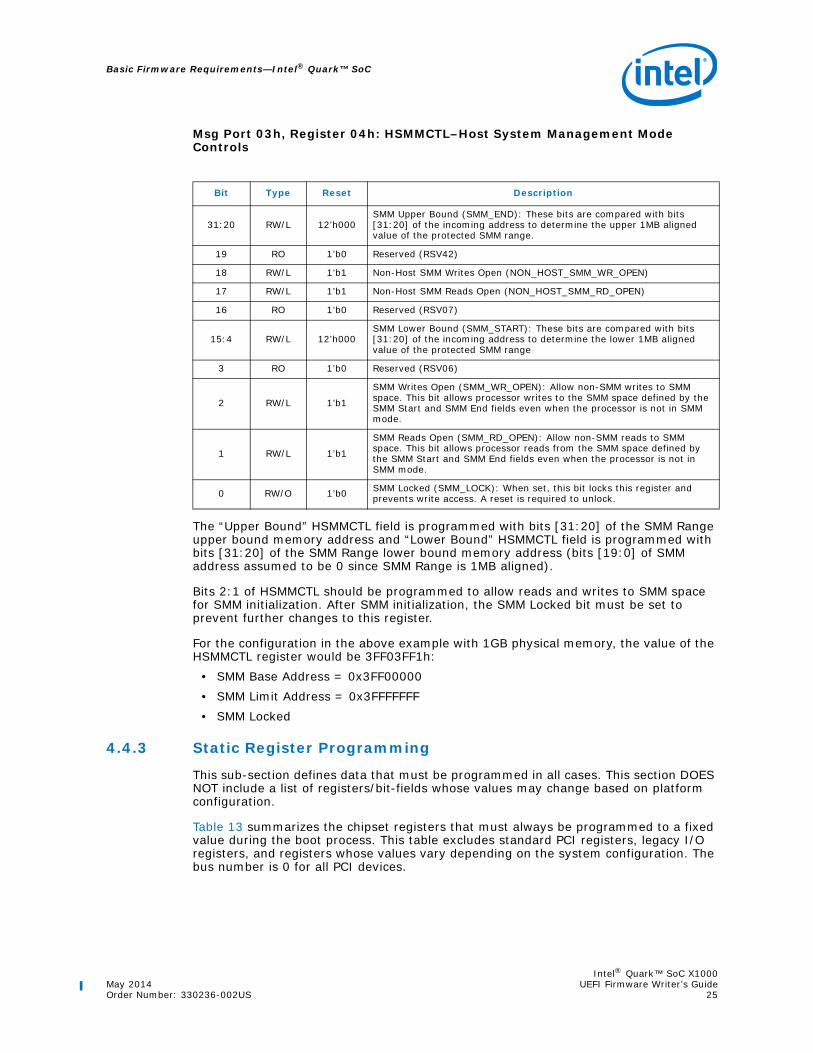
Msg Port 03h, Register 04h: HSMMCTL–Host System Management Mode Controls
The “Upper Bound” HSMMCTL field is programmed with bits [31:20] of the SMM Range upper bound memory address and “Lower Bound” HSMMCTL field is programmed with bits [31:20] of the SMM Range lower bound memory address (bits [19:0] of SMM address assumed to be 0 since SMM Range is 1MB aligned).
Bits 2:1 of HSMMCTL should be programmed to allow reads and writes to SMM space for SMM initialization. After SMM initialization, the SMM Locked bit must be set to prevent further changes to this register.
For the configuration in the above example with 1GB physical memory, the value of the HSMMCTL register would be 3FF03FF1h:
• SMM Base Address = 0x3FF00000• SMM Limit Address = 0x3FFFFFFF• SMM Locked
4.4.3 Static Register Programming
This sub-section defines data that must be programmed in all cases. This section DOES NOT include a list of registers/bit-fields whose values may change based on platform configuration.
Table 13 summarizes the chipset registers that must always be programmed to a fixed value during the boot process. This table excludes standard PCI registers, legacy I/O registers, and registers whose values vary depending on the system configuration. The bus number is 0 for all PCI devices.
Bit Type Reset Description
31:20 RW/L 12’h000SMM Upper Bound (SMM_END): These bits are compared with bits [31:20] of the incoming address to determine the upper 1MB aligned value of the protected SMM range.
19 RO 1’b0 Reserved (RSV42)
18 RW/L 1’b1 Non-Host SMM Writes Open (NON_HOST_SMM_WR_OPEN)
17 RW/L 1’b1 Non-Host SMM Reads Open (NON_HOST_SMM_RD_OPEN)
16 RO 1’b0 Reserved (RSV07)
15:4 RW/L 12’h000SMM Lower Bound (SMM_START): These bits are compared with bits [31:20] of the incoming address to determine the lower 1MB aligned value of the protected SMM range
3 RO 1’b0 Reserved (RSV06)
2 RW/L 1’b1
SMM Writes Open (SMM_WR_OPEN): Allow non-SMM writes to SMM space. This bit allows processor writes to the SMM space defined by the SMM Start and SMM End fields even when the processor is not in SMM mode.
1 RW/L 1’b1
SMM Reads Open (SMM_RD_OPEN): Allow non-SMM reads to SMM space. This bit allows processor reads from the SMM space defined by the SMM Start and SMM End fields even when the processor is not in SMM mode.
0 RW/O 1’b0 SMM Locked (SMM_LOCK): When set, this bit locks this register and prevents write access. A reset is required to unlock.

Intel® Quark™ SoC—Basic Firmware Requirements
Intel® Quark™ SoC X1000UEFI Firmware Writer’s Guide May 201426 Order Number: 330236-002US
Table 13. Generic Static Register Configuration (Sheet 1 of 2)
Name Access Type Address[Bits] Value When to Program
E000h/F000h Routing Message Port
Opcode Pair 10h/11hMsg Port 3h:R03h[2:1]
11bStage 1: Immediately after shadowing (route reads to DRAM)
PCIe* Slot Capabilities PCI D23:F0:R54h[31:0] Platform Specific Stage 2: Before PCI enumeration
PCIe* Slot Capabilities PCI D23:F1:R54h[31:0] Platform Specific Stage 2: Before PCI enumeration
PCIe* Packet Fast Transmit Mode (IPF): PCI D23:F0/F1:RD4h[11] 1b Stage 1: after Memory
Init
PCIe* Message Bus Idle Counter (SBIC): PCI D23:F0/F1:RF4h[17:16] 11b Stage 1: after Memory
Init
PCIe* Upstream Non-Posted Split Disable (UNSD):
PCI D23:F0/F1:RD0h[24] 0b Stage 1: as part of PCIe slot configuration
PCIe* Upstream Non-Posted Request Size (UNRS):
PCI D23:F0/F1:RD0h[15] 1b Stage 1: as part of PCIe slot configuration
PCIe* Upstream Posted Request Size (UPRS):
PCI D23:F0/F1:RD0h[14] 1b Stage 1: as part of PCIe slot configuration
Element Self Descriptor MMIO RCBA + 04h[23:16] 00h Stage 3: Before passing
control to OS
MAC Address Ethernet MAC 0 / MAC1 ADDRLO
MMIO
MAC0 [BAR0] + 44h[31:0]
BAR0 Reference: [B:0, D:20, F:6/F:7] + 10h
Platform Specific Stage 2: After PCI enumeration.
MAC Address Ethernet MAC 0 / MAC1 ADDRHI
MMIO
MAC0 [BAR0] + 40h[15:0]
BAR0 Reference: [B:0, D:20, F:6/F:7] + 10h
Platform Specific Stage 2: After PCI enumeration.
MAC Address Ethernet MAC 0 / MAC1 Address Enable (AE)
MMIO
MAC0 [BAR0] + 40h[31]
BAR0 Reference: [B:0, D:20, F:6/F:7] + 10h
Platform Specific Stage 2: After PCI enumeration.
ASTATUS Message Port
Opcode Pair 10h/11hMsg Port 0h:R21h[1:0]
10b
Stage 1: Before Memory Init
Opcode Pair 10h/11hMsg Port 0h:R21h[3:2]
10b
Opcode Pair 10h/11hMsg Port 0h:R21h[9:8]
11b
Opcode Pair 10h/11hMsg Port 0h:R21h[11:10]
11b
MemoryManager: non host request queue limit.
Message Port
Opcode Pair 10h/11hMsg Port 05h:R20h[5:0]
000010b Stage 1: Before Memory Init

Intel® Quark™ SoC X1000May 2014 UEFI Firmware Writer’s GuideOrder Number: 330236-002US 27
Basic Firmware Requirements—Intel® Quark™ SoC
Chipset Internal Clocks Config
Message Port
Opcode Pair 6h/7hMsg Port 32h:R0140h[22:20]
001b
Stage 1: Before Memory InitSee Note1 below.
Opcode Pair 6h/7hMsg Port 32h:R0140h[25:23]
011b
Opcode Pair 6h/7hMsg Port 32h:R2000h[0]
0b
Opcode Pair 6h/7hMsg Port 32h:R0314h[0]
1b
Opcode Pair 6h/7hMsg Port 32h:R0414h[0]
1b
Opcode Pair 6h/7hMsg Port 32h:R0514h[0]
1b
Notes:1. All READ accesses to registers at port 32h must be followed by 2 identical WRITEs even if the
contents are not to be changed.
Table 13. Generic Static Register Configuration (Sheet 2 of 2)
Name Access Type Address[Bits] Value When to Program

Intel® Quark™ SoC—Basic Firmware Requirements
Intel® Quark™ SoC X1000UEFI Firmware Writer’s Guide May 201428 Order Number: 330236-002US
Table 14. Chipset Thermal Static Register Configuration Sequence
Name Access Type Address[Bits] Value When to Program
Thermal Sensor Mode Config
Message Port
Opcode Pair 06h/07hMsg Port 31h:R31h[5:3]
100b
Stage 1: Before Memory Init
Opcode Pair 06h/07hMsg Port 31h:R31h[12:8]
00010b
Opcode Pair 06h/07hMsg Port 31h:R31h[14]
1b
Opcode Pair 06h/07hMsg Port 31h:R31h[17]
0b
Opcode Pair 06h/07hMsg Port 31h:R31h[18]
0b
Opcode Pair 06h/07hMsg Port 31h:R32h[15:0]
011fh
Opcode Pair 06h/07hMsg Port 31h:R33h[7:0]
17h
Opcode Pair 06h/07hMsg Port 31h:R33h[9:8]
01b
Opcode Pair 06h/07hMsg Port 31h:R33h[31:24]
00h
Opcode Pair 06h/07hMsg Port 31h:R34h[22:11]
0c8h
Thermal Monitor Catastrophic Trip Set Point
Set PointOpcode Pair 10h/11hMsg Port 04h:RB2h[7:0]
Platform Specific See Note1 below
Thermal Monitor Catastrophic Trip Clear Point
Clear PointOpcode Pair 10h/11hMsg Port 04h:RB2h[23:16]
Platform Specific See Note1 below
Take Thermal Sensor out of Reset
Opcode Pair 06h/07hMsg Port 31h:R34h[0]
0b
Enable Thermal Monitor
Opcode Pair 10h/11hMsg Port 04h:RB0h[15]
1b
Lock All Thermal Configuration
Opcode Pair 10h/11hMsg Port 04h:R71h[6:5]
11b
Notes:1. Both fields must be programmed, clear point must be lower then set point and the values in degrees
Celsius is calculated by subtracting an offset of 50 from the 8-bit field value. The temperature in degrees Celsius corresponds to: 00h: -50C, 01h: -49C, ....,FEh: 204C, FFh: 205C

Intel® Quark™ SoC X1000May 2014 UEFI Firmware Writer’s GuideOrder Number: 330236-002US 29
Basic Firmware Requirements—Intel® Quark™ SoC
Table 15. Chipset USB Static Register Configuration Sequence
Name Access Type Address[Bits] Value When to Program
USB2 Global PORT
Message Port
Opcode Pair 06h/07hMsg Port 14h:R4001h[1]
0b
Stage 1: Before Memory Init
Opcode Pair 06h/07hMsg Port 14h:R4001h[8:7]
11b
USB2 COMPBGOpcode Pair 06h/07hMsg Port 14h:R7F04h[10:7]
1001b
USB2 PLL2Opcode Pair 06h/07hMsg Port 14h:R7F03h[29]
1b
USB2 PLL1Opcode Pair 06h/07hMsg Port 14h:R7F02h[1]
1b
USB2 PLL1Opcode Pair 06h/07hMsg Port 14h:R7F02h[6:3]
1000b
USB2 PLL2Opcode Pair 06h/07hMsg Port 14h:R7F03h[29]
0b
USB2 PLL2Opcode Pair 06h/07hMsg Port 14h:R7F03h[24]
1b
USB EHCI Packet Buffer OUT Threshold (OUT_Threshold)
MMIO
USB EHCI [BAR0] + 94h[23:16]
BAR0 Reference: [B:0, D:20, F:3] + 10h
7fh Stage 1: After Memory Init.
USB EHCI Packet Buffer IN Threshold (IN_Threshold)
MMIO
USB EHCI [BAR0] + 94h[7:0]
BAR0 Reference: [B:0, D:20, F:3] + 10h
7fh Stage 1: After Memory Init.
USB Device Interrupt Mask Register (d_intr_msk_udc_reg)
MMIO
USB Device [BAR0] + 0410h[31:0]
BAR0 Reference: [B:0, D:20, F:2] + 10h
0000007fh Stage 1: After Memory Init.
USB Endpoints Interrupt Mask Register (ep_intr_msk_udc_reg)
MMIO
USB Device [BAR0] + 0418h[31:0]
BAR0 Reference: [B:0, D:20, F:2] + 10h
000f000fh Stage 1: After Memory Init.
USB Endpoints Interrupt Register (ep_intr_udc_reg)
MMIO
USB Device [BAR0] + 0414h[31:0]
BAR0 Reference: [B:0, D:20, F:2] + 10h
000f000fh Stage 1: After Memory Init.

Intel® Quark™ SoC—Basic Firmware Requirements
Intel® Quark™ SoC X1000UEFI Firmware Writer’s Guide May 201430 Order Number: 330236-002US
4.5 Remote Management Unit BinaryThe Quark SoC includes a Remote Management Unit that must access its binary data. This binary data is referred to as the RMU binary. The following sections describe the UEFI firmware requirements for handling this RMU binary.
4.5.1 Secure SKU
The RMU binary data is split into two parts (a 2KB RoT binary and a main binary). The location of the RoT binary is hardcoded to FFFE0000h which is located in the Legacy Bridge internal ROM. This 2KB RoT binary is automatically loaded by the Remote Management Unit at power on. During boot, UEFI firmware shadows the main RMU binary data to memory and informs the Remote Management Unit of its location.
4.5.2 Base SKU (Non-Secure)
The location of the RMU binary data is determined by a strap as follows (refer to the [Datasheet] for more details):
• 0b: FFF00000h• 1b: FFD00000h
The first 2KB of the RMU binary is automatically loaded by the RMU at power on. During boot, UEFI firmware shadows the main RMU binary data to memory and informs the Remote Management Unit of its location.
4.6 RMU Binary Relocation After main memory has been either initialized or restored after leaving a suspend state, the RMU binary should be relocated into main system memory to increase system performance.
The firmware build files place a copy of the RMU binary in each of the built stage1 firmware volumes. The firmware finds the binary in the firmware volume using the GUID filename defined by PCD(gEfiQuarkNcSocIdTokenSpaceGuid.PcdQuarkMicrocodeFile) and then copies this binary to main memory. Finally the firmware informs the chipset Remote Management Unit of its location.
Table 16. Chipset PCIe Controller PHY Static Register Configuration Sequence
Name Access Type Address[Bits] Value When to Program
Mixer Load Lane 0Message
Port
Opcode Pair 02h/03hMsg Port 16h:R2080h[7:6]
00b Stage 1: After releasing PCIe controller from resetMixer Load Lane 1
Opcode Pair 02h/03hMsg Port 16h:R2180h[7:6]
00b

Intel® Quark™ SoC X1000May 2014 UEFI Firmware Writer’s GuideOrder Number: 330236-002US 31
Basic Firmware Requirements—Intel® Quark™ SoC
The RMU binary relocation procedure is as follows: 1. Copy the RMU binary (up to 64KB) from Firmware Volume file defined by
PCD(gEfiQuarkNcSocIdTokenSpaceGuid.PcdQuarkMicrocodeFile) to main memory.Note: The RMU binary must be aligned on a 64KB boundary in main memory.
2. Indicate to the chipset that the RMU binary has been copied via the DRAM Base Address Ready register [Opcode 78h:Port 04h, Register 00h]. The data payload should contain the upper 16 bits of the 32 bit DRAM address where the RMU’s 64KB block is located as shown in Table 17.
Figure 2. RMU Binary Relocation
FFFFFFFFh
RMU RoT Binary(2KB)
FFF00000h or FFD00000h (selected by strap)
RMU RoT Binary(2KB)FFFE0000h
FFFFFFFFh
FF800000h
RMU Main Binary(<=64KB)
8MB Legacy SPI Flash 128KB ROM(Only present in
Quark secure SKU)
Address=Don’t Care
• Quark Secure SKU: RMU RoT binary is automatically loaded by hardware from address FFFE0000h in the legacy ROM.• Quark Base SKU (non-secure): RMU RoT binary is automatically loaded by hardware from address FFF00000/FFD00000h in
the legacy SPI Flash.• RMU Main Binary is copied to system memory by UEFI firmware during boot for both secure and base Quark SKUs.
Table 17. DRAM Base Address Ready
Bit Description
31:16 Bit 31:16 of the RMU’s 64KB code block in DRAM
15:00 0000h

Intel® Quark™ SoC—Basic Firmware Requirements
Intel® Quark™ SoC X1000UEFI Firmware Writer’s Guide May 201432 Order Number: 330236-002US
After this procedure is executed, the image located in main memory will be used by the system.
Note: For best system performance, the RMU should be relocated as early as possible after main memory is available.
4.6.1 RMU Binary Relocation Considerations
Firmware must ensure that any OS software does not disturb the integrity of the RMU binary after it has been relocated. The 64KB region that was reserved for the RMU binary must be reported as Reserved in the UEFI memory map.
4.7 PCI/PnP EnumerationSystem firmware is required to perform standard PCI/PnP enumeration and initialize all PCI devices/functions discovered. As part of this process, all PCI-to-PCI bridges (D23:F0-F1) must be initialized with secondary/subordinate bus numbers assigned and bridge windows programmed properly. In addition, I/O, memory, and interrupt resource allocation to PCI devices should be completed.
4.8 ACPI SupportSystem firmware should include ACPI support, with ACPI tables built in memory and reported to the OS.
Before passing control to an ACPI OS, firmware must select the SCI to IRQ mapping by programming the SCIS field (D31:F0:R58h[2:0]). SCI is disabled by default.
4.9 Reporting Interrupt Routing to the OSThe PCI interrupt routing schemes for all motherboard and chipset internal devices, PCI expansion slots and PCI Express* slots behind the root ports are platform specific information. System firmware is required to report this information to the OS via the following interfaces:
• ACPI _PRT packages (per the ACPI Specification, in an ACPI environment)• ACPI Multiple APIC Description Table (per ACPI Specification, in an ACPI
environment)
Refer to these specifications for detailed formats of interrupt routing tables and data structures.
Offset 58h: ACTL – ACPI Control
2:0
SCI IRQ Select (SCIS): Specifies on which IRQ SCI will rout to. If not using APIC, SCI must be routed to IRQ9-11, and that interrupt is not sharable with SERIRQ, but is shareable with other interrupts. If using APIC, SCI can be mapped to IRQ20-23, and can be shared with other interrupts.
Bits SCI Map Bits SCI Map
000 IRQ9 100 IRQ 20
001 IRQ10 101 IRQ 21
010 IRQ11 110 IRQ 22
011 SCI Disabled 111 IRQ 23

Intel® Quark™ SoC X1000May 2014 UEFI Firmware Writer’s GuideOrder Number: 330236-002US 33
Basic Firmware Requirements—Intel® Quark™ SoC
Refer to Section 12.0, “PCI IRQ Routing” on page 64 for details on interrupt routing.
4.10 Reporting IO/Memory Resources to the OSSome of the memory and I/O address ranges used by internal devices are assigned by firmware using base address registers beyond the standard PCI header (above offset 40h), and thus is invisible to OS. Firmware must report such memory/I/O resource usage to OS through standard software interfaces to avoid potential system resource conflict.
Firmware should report the memory address range used by the Chipset Configuration space via UEFI memory table as ’EfiMemoryMappedIO’ memory space (Type=11), and via ACPI _CRS object as motherboard resources, with the device ID of PNP0C02.
Firmware should report all of the I/O register space used by the ACPI, and GPIO devices to the OS by using PNP device node entries and by using ACPI _CRS object. They should be declared as Plug and Play motherboard resources with the Device ID of PNP0C02.
4.11 Chipset Sticky RegistersSticky registers are registers whose contents are preserved during an Intel® Quark™ SoC X1000 warm reset. See definition of warm reset in [Datasheet].
Table 18. Op codes 06h/07h, Msg Port 31h, Offset 51h: CFGSTICKY_RW – Sticky Read/Write
Bit Range Default & Access Description
31:1200000h
RWReserved (RSVD): Reserved.
11:1000bRW
Reserved (RSVD): Reserved.
90bRW
Software Force Recovery (SW_FORCE_RECOVERY): Set by software to indicate a critical error or security violation has been detected and system has warm reset to boot Recovery firmware image.
8:5000bRW
Reserved (RSVD): Reserved.
4 0b RMU Warm Reset (RMU_WARM_RESET): Set by RMU when it initiates a Warm Reset.
3 0b RMU Double ECC error detect (RMU_DECC_DETECT): Set by RMU when it detects a double/multi bit ECC error.
2 0b RMU IMR access violation detect (RMU_IMR_VIOLATION): Set by RMU when it detects a general Isolated Memory Regions (IMRs) access violation.
1 0b RMU HMBOUND access violation detect (RMU_HMB_VIOLATION): Set by RMU when it detects a Host Memory I/O Boundary (HMBOUND) access violation.
0 0b RMU SMM access violation detect (RMU_SMM_VIOLATION): Set by RMU when it detects a System Management Mode (SMM) access violation.

Intel® Quark™ SoC—Basic Firmware Requirements
Intel® Quark™ SoC X1000UEFI Firmware Writer’s Guide May 201434 Order Number: 330236-002US
4.12 Boot ChecklistThe following details the minimum steps necessary to boot using the Quark SoC:
• Control register CR0.NE must be set to 1 as FERR is not supported. Instead native mode will be used (interrupt 16 generated internally on FPU errors).
• Enable NMI operation (IO Port 070h bit 7 = 0).• Enable SMI operation (Msg Port 3:Reg03h bit 13 = 1).• Initialize the legacy SPI decode/enable registers according to platform design
(D31:F0:RD0-D8h).• Relocate and enable early memory for UEFI firmware use (Msg Port 5:Reg82h =
10000080h).• Check resume status (WAKE, PM1_BLK+0, Bit[15]) and SLP_TYP (PM1_BLK + 04h,
Bit[12:10]). If not resuming, take reset path.• Initialize the non-standard BARs (details in Section 4.4.2).• Program GPIO configuration.• Call memory reference code to initialize system memory (details in Section 5.0).• Shadow RMU binary to system memory (see Section 4.6 for details).• Shadow firmware to system memory.• Initialize the “Stage 1” registers in Table 13.• Relocate SMBase, clear SMI status bits at GPE0BASE + 14h, and enable SMIs.• If SMRAM caching is used then a cache flush (wbinvd) must be performed before
exiting SMM. This is required since cache is external to CPU within a Intel® Quark™ SoC X1000.
• Initialize the “Stage 2” registers in Table 13.• Perform PCI enumeration.• Program Sub-System and Sub-Vendor ID in D31:F0:R2Ch. These values are used
as the SSID/SVID for all internal PCI devices. Also program these registers in all PCI Express* devices per PCI specification.
• Initialize the “Stage 3” registers in Table 13.
4.13 UEFI Firmware SourcesThe following table lists the UEFI firmware sources related to the various sections in this chapter.
Section Title File Path Function
4.1Configuring Memory and
MMIO Accesses
QuarkPlatformPkg\Library\QuarkSecLib\Ia32\Flat32.S stackless_EarlyPlatformInit
QuarkPlatformPkg\Library\QuarkSecLib\Ia32\Flat32.asm stackless_EarlyPlatformInit
QuarkPlatformPkg\Platform\Dxe\PlatformInit\PlatformConfig.c PlatformConfigOnSmmConfigurationProtocol
4.2 Early Memory Setup
QuarkPlatformPkg\Library\QuarkSecLib\Ia32\Flat32.S stackless_EarlyPlatformInit
QuarkPlatformPkg\Library\QuarkSecLib\Ia32\Flat32.asm stackless_EarlyPlatformInit
QuarkPlatformPkg\Platform\Dxe\PlatformInit\PlatformConfig.c PlatformConfigOnSmmConfigurationProtocol

Intel® Quark™ SoC X1000May 2014 UEFI Firmware Writer’s GuideOrder Number: 330236-002US 35
Basic Firmware Requirements—Intel® Quark™ SoC
§ §
4.3Isolated
Memory Regions (IMRs)
QuarkPlatformPkg\Platform\Pei\PlatformInit\MrcWrapper.c SetPlatformImrPolicy
QuarkPlatformPkg\Platform\Dxe\PlatformInit\PlatformConfig.c PlatformConfigOnSmmConfigurationProtocol
4.4Initializing
Chipset Registers
QuarkSocPkg\QuarkNorthCluster\Library\IntelQNCLib\IntelQNCLib.cPeiQNCPreMemInit
QNCLockSmramRegionPeiQNCPostMemInit
QuarkPlatformPkg\Library\QuarkSecLib\Ia32\Flat32.S stackless_EarlyPlatformInit
QuarkPlatformPkg\Library\QuarkSecLib\Ia32\Flat32.asm stackless_EarlyPlatformInit
QuarkPlatformPkg\Platform\Pei\PlatformInit\MrcWrapper.c GetMemoryMap
QuarkPlatformPkg\Platform\Pei\PlatformInit\MemoryCallback.c MemoryDiscoveredPpiNotifyCallback
QuarkPlatformPkg\Platform\Dxe\Setup\QNCRegTable.c PlatformInitQNCRegs
QuarkSocPkg\QuarkNorthCluster\Library\IntelQNCLib\PciExpress.c QNCRootPortInit
QuarkPlatformPkg\Platform\Pei\PlatformInit\PlatformEarlyInit.c
EarlyPlatformThermalSensorInit
InitializeUSBPhyPcieControllerEarlyInit
QuarkPlatformPkg\Platform\Pei\PlatformInit\PlatformErratas.c PlatformErratasPostMrc
QuarkPlatformPkg\Platform\Dxe\PlatformInit\PlatformConfig.c SetLanControllerMacAddr
QuarkPlatformPkg\Library\PlatformPcieHelperLib\PlatformPcieHelperLib.c PlatformPciExpressEarlyInit
4.5Remote
Management Unit Binary
QuarkSocPkg\QuarkNorthCluster\Binary\QuarkMicrocode\RMU.bin -
4.6 RMU Binary Relocation
QuarkPlatformPkg\Platform\Pei\PlatformInit\MrcWrapper.c PostInstallMemory
QuarkSocPkg\QuarkNorthCluster\Library\IntelQNCLib\IntelQNCLib.c RmuMainRelocation
4.8 ACPI Support
QuarkPlatformPkg\Platform\Dxe\Setup\QNCRegTable.c PlatformInitQNCRegs
QuarkPlatformPkg\Acpi\Dxe\AcpiPlatform\*.* *.*
QuarkPlatformPkg\Acpi\AcpiTables\*.* *.*
4.9
Reporting Interrupt
Routing to the OS
QuarkPlatformPkg\Acpi\Dxe\AcpiPlatform\MadtPlatform.c *.*
QuarkPlatformPkg\Acpi\AcpiTables\*.* *.*
4.10
Reporting IO/Memory
Resources to the OS
QuarkPlatformPkg\Acpi\AcpiTables\*.* *.*
QuarkSocPkg\QuarkNorthCluster\QNCInit\Dxe\QNCInit.c QNCInitializeResource
QuarkPlatformPkg\Pci\Dxe\PciHostBridge\PciHostBridge.c InitializePciHostBridge
QuarkSocPkg\QuarkNorthCluster\Spi\RuntimeDxe\PchSpi.c InstallPchSpi
Section Title File Path Function

Intel® Quark™ SoC—DDR3 DRAM Configuration
Intel® Quark™ SoC X1000UEFI Firmware Writer’s Guide May 201436 Order Number: 330236-002US
5.0 DDR3 DRAM Configuration
This chapter supplements the information provided in the [Datasheet] for use by firmware vendors and Intel customers developing their own firmware for Quark SoC.
Register locations are referenced in this document, however, the current external design specification or data sheet should be used along with applicable specification updates for obtaining the current register and bit settings of the System Memory Controller.
This document will be supplemented from time to time with specification updates. The specification updates contain information relating to the latest programming changes and may also contain resolutions to known errata. Check with your Intel representative for availability of specification updates.
5.1 Intel® Quark™ SoC System Memory ControllerQuark SoC A0 supports single channel, memory down solution, organized as a single or two ranks of the same DDR3 devices.
For complete details on Intel® Quark™ SoC System Memory Controller capabilities and usage, see the [Datasheet], specifically Section 1.2 and Section 13.0.
5.2 MRC Flow SelectionMemory Reference Code (MRC) is the DRAM/Memory-Controller initialization flow performed by Firmware before DRAM is enabled for functional access.
There are four basic types of MRC flows: • Cold Boot Flow - After transition from G3, G2/S5, G1/S4 state, requires full System
Memory Controller, DDRIO and DRAM initialization sequence and training. Also that flow should be executed on detection of DRAM initialization failure (when GPE0BLK.PMSW.DRAMI bit is set).
• S3 Exit Flow - After transition from G1/S3 state, DRAM is expected to be in self refresh and storing valid data. Training results from last cold boot are used for DDRIO configuration and scrambler vector from last cold boot is written to System Memory Controller.
• Warm Boot Flow- After warm reset some memory subsystem components retain configuration settings, some registers are locked, only partial initialization is required. Training results from last cold boot are used.
• Fast Cold Boot Flow - That is cold boot scenario assuming that memory configuration did not change since the last time. Saved training results are used. The flow must not be used if previous MRC execution indicates error (GPE0BLK.PMSW.DRAMI bit is set).
For further boot flow description they will be referenced as: cold, s3, warm and fast.
In order to detect power transition type, the firmware has to check PM1BLK.PM1S.WAKE and PM1BLK.PM1C.SLPTYPE registers.

Intel® Quark™ SoC X1000May 2014 UEFI Firmware Writer’s GuideOrder Number: 330236-002US 37
DDR3 DRAM Configuration—Intel® Quark™ SoC
The MRC code should use GPE0BLK.PMSW.DRAMI to indicate recent MRC execution status. The bit should be set on MRC entry and cleared on successful completion. This allows detecting memory initialization error and adopting the boot flow in case of failure.
The use of Fast Cold Boot Flow is up to firmware, and can be used to optimize boot performance.
5.3 Programming ConsiderationsMemory initialization requires programming of various registers within different system components. The register/data access is component specific.
See Section 3.1, “Message Network” on page 19.
The message port access is executed using MDR/MCR registers. • D0:F0:RD0h MCR - Message Control Register• D0:F0:RD4h MDR - Message Data Register
5.4 Memory Controller InitializationThis section describes step by step memory initialization sequence, stating the relevance for individual boot flows (cold/S3/warm/fast).
5.4.1 Clear Self-Refresh
Boot flow affected: Cold, Fast, Warm, S3
Clear self-refresh status• PORT1.PMSTS.DISR=1
5.4.2 Program DDR Timing Control
Boot flow affected: Cold, Fast, Warm, S3
Initialize PORT1 DTR0 through DTR4 timing control registers. Follow detailed content description from [Datasheet].
Note: Traditionally DIMM memory characteristic is provided through SPD, that is, providing firmware independence from currently used memory chips. For the soldered down
Table 19. Component-Specific Programming
Component Access method Port Read opcode Write opcode
PORT1System Memory
Controller registersMessage port 0x01 0x10 0x11
PORT5 Message port 0x05 0x10 0x11
DDRIO Message port 0x12 0x06 0x07
MTE Message port 0x11 0x10 0x11
System Memory Controller atomic command handler
Message port 0x01 -- 0x68

Intel® Quark™ SoC—DDR3 DRAM Configuration
Intel® Quark™ SoC X1000UEFI Firmware Writer’s Guide May 201438 Order Number: 330236-002US
DDR3 chips, the memory characteristics are known at production time and can be hard-coded in the firmware.
5.4.3 Program Pre-JEDEC Rank Decoding
Boot flow affected: Cold, Fast
This step is preparing System Memory Controller for executing JEDEC memory initialization sequence.
Disable power saving features and self-refresh• PORT1.DPMC0.CLKGTDIS = 1• PORT1.DPMC0.DISPWRDN = 1• PORT1.DPMC0.DYNSREN = 0• PORT1.DPMC0.PCLSTO = 0
Disable out of order transactions• PORT1.DSCH.OOODIS = 1• PORT1.DSCH.NEWBYPDIS = 1
Disable issuing the REF command• PORT1.DRFC.tREFI = 0
Disable ZQ calibration short• PORT1.DCAL.ZQCINT = 0• PORT1.DCAL.SRXZQCL = 0
Enable rank decoding (depending on ranks populated on the board)• PORT1.DRP.rank0Enabled = 1• PORT1.DRP.rank1Enabled = 1
5.4.4 Perform DDR Reset
Boot flow affected: Cold, Fast
Set COLDWAKE bit before sending the WAKE message (this step is used set up the DDR I/F prior to the JEDEC initialization and to take the System Memory Controller maintenance FSM out of the reset state).
• PORT1.DRMC.COLDWAKE = 1
Using message port access, send wake command (op-code 0xCA) to System Memory Controller (port address 0x01)
Restore default DRMC value• PORT1.DRMC = 0
5.4.5 Initialize DDRIO
Boot flow affected: Cold, Fast, S3
Follow the reference code for the register programming sequence.• The MPLL starts locking immediately after Power Good de-assertion assuming that
the right clock dividers have been passed to the MPLL through straps. There is no

Intel® Quark™ SoC X1000May 2014 UEFI Firmware Writer’s GuideOrder Number: 330236-002US 39
DDR3 DRAM Configuration—Intel® Quark™ SoC
FW action needed to lock the MPLL, but FW intervention is needed in getting the clocks out as the clocks are disabled by default.
• Configure DDR3 interface characteristics through DDRIO registers (specify CL, CWL, read ODT, write RON, write slew rate)
• After all the DDRIO configuration registers have been programmed, Initial RCOMP (DDR Buffer compensation) is enabled.
• After the Initial RCOMP is done, FW enables the clock alignment FSM by a configuration register write.
• FW enables the DDRIO TRANSMIT FIFO pointers.• FW then sets the configuration register for IO_BUFFER_ACTIVATE that will enable
the DDR IO buffers.• FW writes a "1" to the configuration bit to set the DRAM_RESET pad to HIGH• FW writes a "1" to the configuration bit to set the SPID_INIT_COMPLETE bit that is
reflected back to the Memory Controller on the SPID interface.• Now the DDRIO is ready to accept transactions on the SPID interface starting with
the JEDEC initialization of the DDR memory devices.
5.4.6 Perform JEDEC Initialization
Boot flow affected: Cold, Fast
Firmware must ensure the initialization sequence meets JEDEC spec timing intervals. See Reset and Initialization Sequence at Power-on Ramping in [JESD79-3F] for details.
Assert RESET# for 200us• DDRIO.CCDDR3RESETCTL.BIT8=0• DDRIO.CCDDR3RESETCTL.BIT1=1• Wait 200us• DDRIO.CCDDR3RESETCTL.BIT8=1• DDRIO.CCDDR3RESETCTL.BIT1=0
Set CKE signal for each populated memory rank• PORT1.DRMC.CKEVAL[0] = 1• PORT1.DRMC.CKEVAL[1] = 1 // only if 2nd rank populated• PORT1.DRMC.CKEMODE = 1
Send NOP command to each populated rank (using System Memory Controller message for DRAM command (op-code 0x68))
Restore default DRMC value• PORT1.DRMC = 0
For each populated memory rank send MR2, MR3, MR1, MR0 register values and execute ZQCL (using System Memory Controller message for DRAM command (op-code 0x68))
5.4.7 Signal Initialization Complete
Boot flow affected: Cold, Fast, Warm
Specify PRI interface owned by PORT5

Intel® Quark™ SoC—DDR3 DRAM Configuration
Intel® Quark™ SoC X1000UEFI Firmware Writer’s Guide May 201440 Order Number: 330236-002US
• PORT1.DCO.PMICTL = 0
Indicate that initialization of the System Memory Controller has completed. Memory accesses are permitted and maintenance operation begins. Until this bit is set, the memory controller will not accept DRAM requests from the PORT5 or MTE.
• PORT1.DCO.IC = 1
5.4.8 Restore Timings
Boot flow affected: Fast, Warm, S3
Some NV storage is required for storing training results in order to avoid full training procedure on every reset. Assuming use of saved data from the last cold boot flow, program DDRIO settings for:
• Receive enable delay• Read DQS delay• Write DQS delay• Write DQ delay• Internal VREF value• Write control delay• Write clock delay
5.4.9 Disable Memory Caching
Boot flow affected: Cold
During memory training execution, if memory read or write cycles are triggered by the CPU, then caching has to be disabled. Depending on firmware flow, the original values have to be saved and restored after memory training is completed.
Disable DRAM caching• CPU.CR0.CD = 1• MTRR[DRAM_RANGE].TYPE = UC
Flush cache to DRAM• PORT5.BCTRL.MISSVALIDENTRIES = 1• PORT5.BWFLUSH.DIRTY_LWM = 0• PORT5.BWFLUSH.DIRTY_HWM = 0• PORT5.BDEBUG1 = 0• PORT3.HWFLUSH.HWM = 0
5.4.10 Receive Enable Training
Boot flow affected: Cold
The procedure has to be executed for each memory rank and each byte lane.
Adjust internal receive enable signal to the center of the first DQS preamble cycle.
The DQS signal is generated by the DRAM in response to the read command. If the CPU is used to generate read cycles, then read timing has to be extended
• DTR1. tCCD = 1

Intel® Quark™ SoC X1000May 2014 UEFI Firmware Writer’s GuideOrder Number: 330236-002US 41
DDR3 DRAM Configuration—Intel® Quark™ SoC
in order to be able to sample DQS preamble.
Using default back-to-back transactions, it is not possible to capture DQS preamble. Single CPU memory read generates 4 read commands on the DDR interface, DQS samples are collected from the last read. After completed receive enable training, DTR1 settings have to be restored.
For individual byte lanes, the DQS sample is read from • DDRIO.Reg0x0034.Bit0 - byte lane 0• DDRIO.Reg0x0034.Bit1 - byte lane 1
For the purpose of the training algorithm, the representative sample value should be evaluated as the average of multiple samples.
The receive enable delay is expressed in 1/128 of memory clock cycle duration. The final value is the result of the following formula:
• DDRIO.Reg0x0070.Bit[11:08]*64 + DDRIO.Reg0x003C.Bit[29:24] - byte lane 0• DDRIO.Reg0x0070.Bit[23:20]*64 + DDRIO.Reg0x0038.Bit[29:24] - byte lane 1
Dead band adjust (additional configuration is required if delay is outside of certain limits, otherwise referenced bits should be set to zero).
If DDRIO.Reg0x003C.Bit[29:24] is less than 0x12 or greater than 0x34 then• DDRIO.Reg0x007C.Bit5 = 1
If DDRIO.Reg0x003C.Bit[29:24] is less than 0x12 then• DDRIO.Reg0x007C.Bit11 = 1
If DDRIO.Reg0x0038.Bit[29:24] is less than 0x12 or greater than 0x34 then• DDRIO.Reg0x007C.Bit2 = 1
If DDRIO.Reg0x0038.Bit[29:24] is less than 0x12 then• DDRIO.Reg0x007C.Bit8 = 1
Algorithm overview:• Start with arbitrary delay• Increase delay with small steps in order to detect DQS sample change 0'1• Increase delay by 32 to place in center of high pulse• Decrease delay by 128 (entire memory clock) until zero is sampled (i.e. DQS
preamble)• Increase delay by 32 to position receive enable at the middle of the DQS preamble
cycle• As the setting is common for both ranks, the final result must be the average.
5.4.11 Write Leveling Training
Boot flow affected: Cold
The procedure has to be executed for each memory rank and each byte lane.
Adjust write DQS signal delay to DRAM clock (fine write leveling).
Adjust write DQ delay to write DQS signal in order to get write and read consistency for simple data patterns (coarse write leveling).

Intel® Quark™ SoC—DDR3 DRAM Configuration
Intel® Quark™ SoC X1000UEFI Firmware Writer’s Guide May 201442 Order Number: 330236-002US
Fine write leveling
The write DQS delay is expressed in 1/128 of memory clock cycle duration. The final delay is result of the following formula:
• DDRIO.Reg0x0070.Bit[07:04]*64 + DDRIO.Reg0x003C.Bit[21:16] - byte lane 0• DDRIO.Reg0x0070.Bit[19:16]*64 + DDRIO.Reg0x0038.Bit[21:16] - byte lane 1
Dead band adjust (additional configuration is required if delay is outside of certain limits, otherwise referenced bits should be set to zero).
If DDRIO.Reg0x003C.Bit[21:16] is less than 0x12 or greater than 0x34 then• DDRIO.Reg0x007C.Bit1 = 1
If DDRIO.Reg0x003C.Bit[21:16] is less than 0x12 then• DDRIO.Reg0x007C.Bit4 = 1
If DDRIO.Reg0x0038.Bit[21:16] is less than 0x12 or greater than 0x34 then• DDRIO.Reg0x007C.Bit7 = 1
If DDRIO.Reg0x0038.Bit[21:16] is less than 0x12 then• DDRIO.Reg0x007C.Bit10 = 1
In write leveling mode, the memory is providing internal clock state on the DQ lines as it is latched by the rising edge of write DQS signal. The sample of DQ signals can be read from:
• DDRIO.Reg0x0034.Bit8 - byte lane 0• DDRIO.Reg0x0034.Bit9 - byte lane 1
Algorithm• Perform a single PRECHARGE ALL command to make DRAM state machine go to
IDLE state• Enable write leveling mode in MRS1• Set PORT1.DTR4.ODTDIS = 1 (ODT disable)• Configure DDRIO write leveling mode
— DDRIO.Reg0x009C = ((DDRIO.Reg0x009C & 0x100003FC) | 0x10000154)— DDRIO.Reg0x5830.Bit16 = 1
• Set arbitrary delay for write DQS signal• Increase delay with small steps in order to detect DQ sample change 0'1• Cancel DDRIO write leveling mode
— DDRIO.Reg0x5830.Bit16 = 0— DDRIO.Reg0x009C = ((DDRIO.Reg0x009C & 0x100003FC) | 0x00000154)
• Set PORT1.DTR4.ODTDIS = 0 (ODT enable)• Disable write leveling mode in MRS1• Perform a single PRECHARGE ALL command to make DRAM state machine go to
IDLE state

Intel® Quark™ SoC X1000May 2014 UEFI Firmware Writer’s GuideOrder Number: 330236-002US 43
DDR3 DRAM Configuration—Intel® Quark™ SoC
Coarse write leveling
During coarse write leveling, write DQ delay has to be set ¼ DCLK (128/4 = 32 units) earlier than write DQS, then write DQS is moved by the whole DCLK (128 units) until read data is matching write data. Simple (low frequency) data pattern has to be used for write/read test.
The delay has to be adjusted for each byte lane, and finally the average (per byte lane) from all ranks has to be programmed.
The write DQ delay is expressed in 1/128 of memory clock cycle duration. The final value is the result of the following formula:
• DDRIO.Reg0x0070.Bit[03:00]*64 + DDRIO.Reg0x003C.Bit[13:08] - byte lane 0• DDRIO.Reg0x0070.Bit[15:12]*64 + DDRIO.Reg0x0038.Bit[13:08] - byte lane 1
Dead band adjust (additional configuration is required if delay is outside of certain limits, otherwise referenced bits should be set to zero).
If DDRIO.Reg0x003C.Bit[13:08] is less than 0x12 or greater than 0x34 then• DDRIO.Reg0x007C.Bit0 = 1
If DDRIO.Reg0x003C.Bit[13:08] is less than 0x12 then• DDRIO.Reg0x007C.Bit3 = 1
If DDRIO.Reg0x0038.Bit[13:08] is less than 0x12 or greater than 0x34 then• DDRIO.Reg0x007C.Bit6 = 1
If DDRIO.Reg0x0038.Bit[13:08] is less than 0x12 then• DDRIO.Reg0x007C.Bit9 = 1
5.4.12 Read Training
Boot flow affected: Cold
The procedure has to be executed for each memory rank and each byte lane.
Find available margins for internal VREF value and read DQS delay and position these signals in the "eye" center. The margining is executed by verifying successful read of random write patterns.
Algorithm• (A) Starting from min VREF, find min working read DQS passing write/read test.
Increase VREF if no valid read DQS can be found.• (B) Starting from min VREF, find max working read DQS. Increase VREF if no valid
read DQS can be found.• (C) Starting from max VREF, find min working read DQS. Decrease VREF if no valid
read DQS can be found.• (D) Starting from max VREF, find max working read DQS. Decrease VREF if no valid
read DQS can be found.• Calculate average read DQS for min working VREF (using A & B step results)• Calculate average read DQS for max working VREF (using C & D step results)• Configure final read DQS using average from above results • Calculate average VREF for min read DQS (using A & C step results)

Intel® Quark™ SoC—DDR3 DRAM Configuration
Intel® Quark™ SoC X1000UEFI Firmware Writer’s Guide May 201444 Order Number: 330236-002US
• Calculate average VREF for max read DQS (using B & D step results)• Configure final VREF using average from above results
Note: Finally average result from each rank should be used.
The read DQS delay is expressed in 1/128 of memory clock cycle duration. The final value is result of the following formula:
• DDRIO.Reg0x005C.Bit[06:00] - byte lane 0• DDRIO.Reg0x0058.Bit[06:00] - byte lane 1
The value of VREF is programmed in the following register:• DDRIO.Reg0x0014.Bit[07:02] - byte lane 0• DDRIO.Reg0x0024.Bit[07:02] - byte lane 1
Min to max VREF encoding: 0x3F, …,0x20, 0x00, …,0x1F
5.4.13 Write Training
Boot flow affected: Cold
The procedure has to be executed for each memory rank and each byte lane.
Find available margins for write DQ signal and position it in the "eye" center. The margining is executed by verifying successful write of random data patterns.
Algorithm• Starting from write DQ delay configured ¼ DCLK earlier than write DQS (using the
results from coarse write leveling), find min and max write DQ delay passing the write/read test.
• Configure final write DQ delay as the average of the above results
5.4.14 Store Timings
Boot flow affected: Cold
Training results collected during cold boot flow should be saved in some NV storage for later use (i.e. for Fast, Warm, and S3 flows, see Section 5.4.8, “Restore Timings” on page 40).
5.4.15 Enable Scrambling
Boot flow affected: Cold, Fast, Warm, S3
If scrambling is enabled by platform designer/owner, then the Firmware should load a new, random scrambler vector every cold boot. At S3 Exit, the Firmware must load the same vector loaded in the last cold boot since the DRAM is expected to contain valid data and the same scrambler vector that was used to write the data into the DRAM is needed to unscramble it.
• PORT1.SCRMSEED = random_value
5.4.16 Program Execution Control
Boot flow affected: Cold, Fast, Warm, S3

Intel® Quark™ SoC X1000May 2014 UEFI Firmware Writer’s GuideOrder Number: 330236-002US 45
DDR3 DRAM Configuration—Intel® Quark™ SoC
Configure power management• PORT1.DPMC0.CLKGTDIS = 0• PORT1.DPMC0.DISPWRDN = 0• PORT1.DPMC0.PCLSTO = 4• PORT1.DPMC0.PREAPWDEN = 1
Configure scheduler control registers • PORT1.DSCH.OOODIS = 0• PORT1.DSCH.OOOST3DIS = 0• PORT1.DSCH.NEWBYPDIS = 0
5.4.17 Configure Rank Population
Boot flow affected: Cold, Fast, Warm, S3
After training is completed, configure System Memory Controller rank population register specifying: enabled ranks, device width, density, and address mode.
• PORT1.DCO.IC = 0• PORT1.DRP.rank0Enabled = 1• PORT1.DRP.rank1Enabled = rank1_present• PORT1.DRP.dimm0DevWidth = dev0_width• PORT1.DRP.dimm1DevWidth = dev1_width• PORT1.DRP.dimm0DevDensity = dev0_density• PORT1.DRP.dimm1DevDensity = dev1_density• PORT1.DRP.addressMap = address_mode
Signal initialization complete• PORT1.DCO.IC = 1
5.4.18 Perform Wake
Boot flow affected: Warm, S3
Using Message Network+, send the wake command (op-code 0xCA) to System Memory Controller (port address 0x01)
5.4.19 Change Refresh Period
Boot flow affected: Cold, Fast, Warm, S3
Configure refresh rate and short ZQ calibration interval. Activate dynamic self-refresh.• PORT1.DRFC.tREFI = refresh_rate• PORT1.DRFC.REFDBTCLR = 1• PORT1.DCAL.ZQCINT = 3• PORT1.DPMC0.ENPHYCLKGATE = 1• PORT1.DPMC0.DYNSREN = 1

Intel® Quark™ SoC—DDR3 DRAM Configuration
Intel® Quark™ SoC X1000UEFI Firmware Writer’s Guide May 201446 Order Number: 330236-002US
5.4.20 Set Periodic Compensation
Boot flow affected: Cold, Fast, Warm, S3
Configure DDRIO for Periodic Compensations, Dynamic Diff-Amp
Enable Periodic RCOMPS• DDRIO.Reg0x6800.BIT1 = 1
Enable Dynamic Diff-Amp and ODT• DDRIO.Reg0x0094 &= ~0x3FFC00• DDRIO.Reg0x0098 &= ~0x3FFC00
For each populated rank sent ZQCS command• MDR = (RNK << 22) | 6• MCR = 0x680100F0
Reset internal DDRIO FIFO pointers• DDRIO.Reg0x0074.BIT8 = 0• DDRIO.Reg0x0074.BIT8 = 1
5.4.21 Enable ECC
Boot flow affected: Cold, Fast, Warm, S3
Depending on configuration enable ECC support. Note that some Intel® Quark™ SoC SKUs do not support ECC. Even if ECC is supported by the silicon, the designer may decide not to use it because of boot performance impact (required entire memory cleanup for initial ECC reset) or because of related memory bandwidth and size limitation.
Force settings required for ECC• PORT1.DRP.addressMap = 2• PORT1.DRP.split64 = 1• PORT1.DSCH.NEWBYPDIS = 1
Enable ECC• PORT1.DECCCTRL.SBEEN = 1• PORT1.DECCCTRL.DBEEN = 1• PORT1.DECCCTRL.ENCBGEN = 1
Available memory size is decreased as part of it is used to store ECC, and is not available for use by the system (see [Datasheet] for details).
• AvailableMemSize = ActualMemSize * 7 / 8
Clear available memory in order to initialize ECC (except of S3 flow, as memory content has to be preserved).
5.4.22 Memory Test
Boot flow affected: Cold, Fast, Warm

Intel® Quark™ SoC X1000May 2014 UEFI Firmware Writer’s GuideOrder Number: 330236-002US 47
DDR3 DRAM Configuration—Intel® Quark™ SoC
Memory test is optional. In case of Fast/Warm boot flows, as recovery from the test failure, the complete memory training might be executed.
5.4.23 Lock Registers
Boot flow affected: Cold, Fast, Warm, S3
For security purposes, at the end of memory initialization, changes to the DRP register and MTE access must be disabled.
• PORT1.DCO.PMIDIS = 0• PORT1.DCO.PMICTL = 0• PORT1.DCO.DRPLOCK = 1• PORT1.DCO.REUTLOCK = 1
5.5 Memory Training EngineThe MTE (Memory Training Engine) is part of the System Memory Controller. It can be used during memory initialization and training as it offers better performance comparing to CPU driven memory access. The reference code provides primitive functions supporting:
• ECC initialization - Fill memory with fixed pattern• Memory test - Write, and then read/verify entire memory using fixed pattern • Coarse write leveling - Write, and then read/verify at specified address, using low
frequency pattern• Read and write training - Write, and then read/verify at specified address, using
variable random patterns
The control over DDR interface, SoC vs. MTE, depends on the PORT1.DCO.PMICTL bit state.
5.6 Memory Reference Code ConfigurationIntel® Quark™ SoC MRC is implemented in the MemoryInitPei component, being part of QuarkSocPkg package. The memory controller initialization is performed by MemoryInit function with respect to the current boot flow mode. That function is executed at the end of PEI phase (indirectly through the service protocol interface call). The platform specific code has to provide all required input data through the MRC_PARAMS structure (see definition in QuarkSocPkg\QuarkNorthCluster\MemoryInit\Pei\mrc.h).
The MRC_PARAMS structure input data to the MRC is set up by the MemoryInit, MrcConfigureFromMcFuses and MrcConfigureFromInfoHob of QuarkPlatformPkg\Platform\Pei\PlatformInit\MrcWrapper.c
The reference platform design assumes "memory down" solution, thus the configuration is fixed for a specific platform, and no external or discrete SPD data is used.
Certain parameters may be fixed by silicon fuses (see MrcConfigureFromMcFuses). Configurable parameters are modified using platform data stored in legacy SPI flash. For example, configurable parameters include number of populated ranks, DDR width, density, clock speed, etc. The default timing parameters are based on JESD79-3E specification and are specific to DDR clock speed and data bus width. The PDAT_MRC_ITEM structure in QuarkPlatformPkg\include\PlatformData.h defines MRC configuration parameters stored in platform data. Refer to [Build Guide] for more

Intel® Quark™ SoC—DDR3 DRAM Configuration
Intel® Quark™ SoC X1000UEFI Firmware Writer’s Guide May 201448 Order Number: 330236-002US
details on platform data.
5.7 UEFI Firmware SourcesThe following table lists the UEFI firmware sources related to the various sections in this chapter.
§ §
Section Title File Path Function/structures
5.0DDR3 DRAM Configuration
QuarkSocPkg\QuarkNorthCluster\MemoryInit\Pei\*.* *.*
QuarkPlatformPkg\Platform\Pei\PlatformInit\MrcWrapper.c MemoryInit
QuarkPlatformPkg\Platform\Pei\PlatformInit\MrcWrapper.c
MrcConfigureFromMcFuses
QuarkPlatformPkg\Platform\Pei\PlatformInit\MrcWrapper.c
MrcConfigureFromInfoHob
QuarkPlatformPkg\include\PlatformData.h PDAT_MRC_ITEM structure

Intel® Quark™ SoC X1000May 2014 UEFI Firmware Writer’s GuideOrder Number: 330236-002US 49
CPUID Instruction—Intel® Quark™ SoC
6.0 CPUID Instruction
For a detailed description of the CPUID instruction format, please refer to the Intel® Architecture Software Developer's Manual. This section provides additional documentation specific to the Quark SoC. The UEFI firmware should use the CPUID instruction to identify the Quark SoC.
Two sets of functions are supported: standard functions, and extended functions. The standard functions are 0000_0000h - 0000_000Bh. The extended functions are 8000_0000h and above.
6.1 CPUID FunctionsQuark SoC UEFI firmware uses the CPUID instruction to determine what features are supported by the Quark SoC. The UEFI firmware should validate the Vendor-ID before executing additional CPUID functions (must return ’GenuineIntel’). Table 20 lists the CPUID functions supported on Quark SoC.
Table 20. Intel® Quark™ SoC CPUID Functions (Sheet 1 of 2)
CPUID Function Number (EAX Value)
Returned on Intel® Quark™ SoC Description
0x00000000
EAX=0x00000007 Largest standard CPUID function number supported.
EBX=0x756E6547 ’uneG’. Part of ’GenuineIntel’ string
ECX=0x6C65746E ’letn’. Part of ’GenuineIntel’ string
EDX=0x49656E69 ’Ieni’. Part of ’GenuineIntel’ string
0x00000001
EAX=0x00000590 Family ID=0x5, Model=0x9, Stepping ID=0x0
EBX=0x00010000
[7:0] = Brand ID.[15:8] = CLFLUSH line size.[23:16] = Maximum number of logical processors per package.[31:24] = Default APIC ID.
ECX=0x00000000 Features supported
EDX=0x8000237B
[0] = FPU on chip[1] = Virtual 8086 mode enhancements[3] = PSE. Page Size Extension. Large pages of size 4MB are supported including CR4.PSE[4] = TSC. Time Stamp Counter. RDTSC instruction is supported including CR4.TSD for controlling privilege.[5] = MSR. Model Specific Register RDMSR/WRMSR instructions.[6] = PAE. Physical Address Extension.[8] = CMXCHG8B instruction support.[9] = APIC. APIC on chip[13] = PGE. Page Global Bit[31] = PBE. Pending Break Event.

Intel® Quark™ SoC—CPUID Instruction
Intel® Quark™ SoC X1000UEFI Firmware Writer’s Guide May 201450 Order Number: 330236-002US
0x00000002
EAX=0x00000001[0] = Number of CPUIDsNo cache information to report.
EBX=0x00000000 No cache information to report.
ECX=0x00000000 No cache information to report.
EDX=0x00000000 No cache information to report.
0x00000003 - 0x00000006
EAX=0x00000000
EBX=0x00000000
ECX=0x00000000
EDX=0x00000000
0x00000007 (and ECX=0x00000000)
EAX=0x00000001 Maximum number of supported leaf 7 sub leaves
EBX=0x00000080 or 0x00000000 [7] = SMEP
ECX=0x00000000
EDX=0x00000000
0x00000007 (and ECX!=0x00000000)
EAX=0x00000000
EBX=0x00000000
ECX=0x00000000
EDX=0x00000000
0x80000000
EAX=0x80000008 Maximum extended CPUID function
EBX=0x00000000
ECX=0x00000000
EDX=0x00000000
0x80000001
EAX=0x00000000
EBX=0x00000000
ECX=0x00000000
EDX=0x00100000 or 0x00000000
[20] = Execute Disable available.0: if IA32_MISC_ENABLES[34]=11: if IA32_MISC_ENABLES[34]=0
0x80000002 - 0x80000007
EAX=0x00000000
EBX=0x00000000
ECX=0x00000000
EDX=0x00000000
0x80000008 EAX=0x00002020[7:0] = Physical address width[15:8] = Linear address width
EBX=0x00000000
ECX=0x00000000
EDX=0x00000000
Table 20. Intel® Quark™ SoC CPUID Functions (Sheet 2 of 2)
CPUID Function Number (EAX Value)
Returned on Intel® Quark™ SoC Description
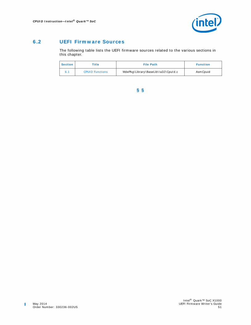
Intel® Quark™ SoC X1000May 2014 UEFI Firmware Writer’s GuideOrder Number: 330236-002US 51
CPUID Instruction—Intel® Quark™ SoC
6.2 UEFI Firmware SourcesThe following table lists the UEFI firmware sources related to the various sections in this chapter.
§ §
Section Title File Path Function
6.1 CPUID Functions MdePkg\Library\BaseLib\Ia32\CpuId.c AsmCpuid

Intel® Quark™ SoC—Model Specific Registers
Intel® Quark™ SoC X1000UEFI Firmware Writer’s Guide May 201452 Order Number: 330236-002US
7.0 Model Specific Registers
Quark SoC supports a subset of Model Specific Registers (MSRs). These MSRs and the supported bits are listed in Table 21.
UEFI firmware must ensure IA32_MISC_ENABLE[22]=0 so that all CPUID functions are reported.
7.1 UEFI Firmware SourcesThe following table lists the UEFI firmware sources related to the various sections in this chapter.
§ §
Table 21. Model Specific Registers
Name Address Feature Bit definition
IA32_TSC 0x10 Time Stamp CounterThis is a 64-bit counter that increments with the core clock frequency.
IA32_MISC_ENABLE 0x1A0 PAE/XD
[22]=Limit CPUID[34]=XD DisableAll other bits are reserved. Writing of 1'b1 to reserved bits causes #GP(0) Fault.
IA32_EFER 0xC000_0080 PAE/XD
[11] - NXE - Execute Disable bit Enable.All other bits are reserved. Writing of 1'b1 to reserved bits causes #GP(0) Fault.
Section Title File Path Function
7.0Model
Specific Registers
IA32FamilyCpuBasePkg\CpuMpDxe\LimitCpuIdValue.c MaxCpuidLimitReg
QuarkSocPkg\Override\MdePkg\Library\BaseLib\ReadMsr64.c AsmReadMsr64
QuarkSocPkg\Override\MdePkg\Library\BaseLib\WriteMsr64.c AsmWriteMsr64
QuarkSocPkg\Override\MdePkg\Library\BaseLib\QuarkMsr.c TranslateMsrIndex
MdePkg\Library\BaseLib\Ia32\ReadTsc.cQuarkSocPkg\Override\MdePkg\Library\BaseLib\Ia32\GccInline.c AsmReadTsc

Intel® Quark™ SoC X1000May 2014 UEFI Firmware Writer’s GuideOrder Number: 330236-002US 53
System Management Mode (SMM)—Intel® Quark™ SoC
8.0 System Management Mode (SMM)
System Management Mode (SMM) is a high priority mode of the Quark SoC that is entered when the Quark SoC acknowledges a System Management Interrupt (SMI). When the Quark SoC enters SMM it writes the current state of the Quark SoC (the Quark SoC’s context) to memory and begins executing specialized UEFI firmware code. When entering SMM the Quark SoC is in a mode similar to real-address mode except there are no privilege levels or address mapping. The main benefit of SMM is that it offers a distinct and easily isolated processor environment that operates transparently to the operating system or executive and software applications. SMM has proven valuable as a mechanism for working around various system issues and also for power management handling. However, if not used correctly, SMM has the ability to cause unexpected system behavior, poor system performance and even crash/hang the operating system.
The Quark SoC introduces new capabilities and requirements for SMM. This chapter discusses UEFI firmware changes required to supported SMM.
For a detailed overview of SMM, refer to the Intel® 64 and IA-32 Architectures Software Developer’s Manual, Volume 3A: System Programming Guide, Part 1.
8.1 Initializing SMMDuring the boot process, the bootstrap processor (BSP) is responsible for:
• Configuring the chipset controls (see SMM Control in Table 12) for the SMM region.• Copying the runtime SMM handler to the TSEG.• Copying the SMM relocation handler to 30000h + 8000h.• Invoking an SMI IPI (Inter Processor Interrupt, see Section 16.0) to self to execute
the SMM relocation handler.• Resume execution of the boot process.
Since the BSP initialized the chipset and installed the runtime SMM handler, the application processors (APs) must:
• Send an SMI IPI to self to execute the SMM relocation handler. This first SMI will cause the Quark SoC to vector to 30000h + 8000h.
• Resume execution of the multiprocessor initialization.
8.1.1 Responsibilities of the SMM Relocation Handler
For each logical processor, the first SMI it receives after a reset will cause the processor to vector to 30000h + 8000h. This is the default SMBASE for all Intel processors. UEFI firmware is responsible for relocating this default SMBASE to be located in TSEG memory space. Each logical processor must be assigned a unique SMBASE in TSEG. Thus, UEFI firmware installs the SMM Relocation Handler at this default SMBASE. The SMM relocation handler is responsible for:
— Assigning each processor a unique SMBASE. The SMBASE is only configurable while in SMM and must be written to the SMBASE register which is

Intel® Quark™ SoC—System Management Mode (SMM)
Intel® Quark™ SoC X1000UEFI Firmware Writer’s Guide May 201454 Order Number: 330236-002US
part of the processor context saved when the SMI was acknowledged. The SMBASE register during this first SMI is located at memory address 30000h + (8000h + 7EF8h). Subsequent SMIs will cause the processor to vector to the new SMM entry point which is SMBASE + 8000h. The minimum distance between adjacent SMBASE assignments is 200h (512) bytes. The Quark SoC SMBASE must be aligned on a 32KB boundary.
— Configuring the System Management Mode Range Registers (SMRR). The SMRR maps the cacheability of the runtime SMM handler. The runtime handler must be located in TSEG. The SMRRs enhance SMM by making the SMM memory cacheable upon acknowledging an SMI. The SMRR is used to define the cacheability type of all of the TSEG. SMRAM base and size must be aligned on a power of 2 boundary. Since TSEG is now cacheable when the processor is writing its context, entry and exit of the runtime SMM handler should be faster. Refer to Section 9.2.1 for additional details.
During the boot process, the UEFI firmware must initialize the SMBASE for each logical processor in the Quark SoC. Each logical processor must be assigned a unique SMBASE aligned on a 32KB boundary. The SMBASE for a logical processor must maintain at least 200h address separation from another logical processor’s SMBASE.
The address selected for SMBASE relocation must not overlap fixed Local APIC range (FEE00000h-FEEFFFFFh).
8.2 SMM Revision IdentifierUpon entering SMM, the UEFI firmware must check the SMMREV_ID register located at SMBASE + 8000h + 7EFCh. The Quark SoC supports a SMMREV_ID of 3_0000h.
8.3 SMM State Save Map The Quark SoC supports 32-bit SMM State Save Map.
Table 22. SMRAM State Save Map (Sheet 1 of 2)
Offset (Added to SMBASE + 8000H) Register Writable?
7FFCH CR0 No
7FF8H CR3 No
7FF4H EFLAGS Yes
7FF0H EIP Yes
7FECH EDI Yes
7FE8H ESI Yes
7FE4H EBP Yes
7FE0H ESP Yes
7FDCH EBX Yes
7FD8H EDX Yes
7FD4H ECX Yes
7FD0H EAX Yes
7FCCH DR6 No
7FC8H DR7 No
† The two most significant bytes are reserved.

Intel® Quark™ SoC X1000May 2014 UEFI Firmware Writer’s GuideOrder Number: 330236-002US 55
System Management Mode (SMM)—Intel® Quark™ SoC
8.4 SMRR Configuration RequirementsConfiguring the SMRR registers only occurs during the first SMI per logical processor where SMM relocation of the SMBASE is accomplished. SMRR configuration is NOT executed with each subsequent SMI.
Note: Configuration of SMRR is discussed in Section 9.2.1. SMRR can only be configured while the processor is in SMM and executing the SMM relocation handler.
7FC4H TR† No
7FC0H Reserved No
7FBCH GS† No
7FB8H FS† No
7FB4H DS† No
7FB0H SS† No
7FACH CS† No
7FA8H ES† No
7FA4H I/O State Field No
7FA0H I/O Memory Address Field No
7F9FH-7F03H Reserved No
7F02H Auto HALT Restart Field (Word) Yes
7F00H I/O Instruction Restart Field (Word) Yes
7EFCH SMM Revision Identifier Field (Doubleword) No
7EF8H SMBASE Field (Doubleword) Yes
7EF7H - 7E00H Reserved No
Table 22. SMRAM State Save Map (Sheet 2 of 2)
Offset (Added to SMBASE + 8000H) Register Writable?
† The two most significant bytes are reserved.

Intel® Quark™ SoC—System Management Mode (SMM)
Intel® Quark™ SoC X1000UEFI Firmware Writer’s Guide May 201456 Order Number: 330236-002US
8.5 UEFI Firmware SourcesThe following table lists the UEFI firmware sources related to the various sections in this chapter.
§ §
Section Title File Path Function
8.1 Initializing SMM
QuarkPlatformPkg\Platform\Pei\PlatformInit\MrcWrapper.c GetMemoryMap
QuarkSocPkg\\QuarkNorthCluster\Library\IntelQNCLib\IntelQNCLib.c QNCGetTSEGMemoryRange
QuarkSocPkg\QuarkNorthCluster\Library\IntelQNCLib\IntelQNCLib.c QNCOpenSmramRegion
QuarkSocPkg\QuarkNorthCluster\Library\IntelQNCLib\IntelQNCLib.c QNCCloseSmramRegion
QuarkSocPkg\QuarkNorthCluster\Library\IntelQNCLib\IntelQNCLib.c QNCLockSmramRegion
IA32FamilyCpuBasePkg\PiSmmCpuDxeSmm\Ia32\SmmInit.asmIA32FamilyCpuBasePkg\PiSmmCpuDxeSmm\Ia32\SmmInit.S SmmStartup
IA32FamilyCpuBasePkg\PiSmmCpuDxeSmm\PiSmmCpuDxeSmm.cSmmRelocateBases
SmmInitHandlerFindSmramInfo
IA32FamilyCpuBasePkg\PiSmmCpuDxeSmm\Ia32\SmiEntry.asmIA32FamilyCpuBasePkg\PiSmmCpuDxeSmm\Ia32\SmiEntry.S _SmiEntryPoint
IA32FamilyCpuBasePkg\PiSmmCpuDxeSmm\MpService.c SmiRendezvous
IA32FamilyCpuBasePkg\PiSmmCpuDxeSmm\SmmFeatures.c
IsSmrrSupportedPentiumInitSmrr
DisableSmrrPentiumEnableSmrr
8.2 SMM Revision Identifier
IntelFrameworkPkg\Include\Protocol\SmmCpuSaveState.h EFI_SMM_CPU_STATE32.SMMRevId
IA32FamilyCpuBasePkg\PiSmmCpuDxeSmm\PiSmmCpuDxeSmm.c SmmReadSaveState
8.3 SMM State Save Map
IntelFrameworkPkg\Include\Protocol\SmmCpuSaveState.h EFI_SMM_CPU_STATE32
IA32FamilyCpuBasePkg\PiSmmCpuDxeSmm\PiSmmCpuDxeSmm.c SmmReadSaveState
8.4SMRR
Configuration Requirements
IA32FamilyCpuBasePkg\PiSmmCpuDxeSmm\SmmFeatures.c SmmInitiFeatures

Intel® Quark™ SoC X1000May 2014 UEFI Firmware Writer’s GuideOrder Number: 330236-002US 57
Cache Control—Intel® Quark™ SoC
9.0 Cache Control
9.1 MTRR ProgrammingQuark SoC does not support MSR MTRRs. Fixed and Variable range MTRRs are accessed via the Message Network Registers (refer to Section 4.4) and not the traditional MSR mechanism. Refer to the [Datasheet] for more details. The following are the Cache types supported by the Quark SoC.
In addition to setting up the decoding of the E0000h and F0000h segments, system firmware should also program the MTRR (Memory Type Range Registers), which are part of the Quark SoC. The following are the suggested MTRR settings for various memory regions.
Note: The programming described in Table 24 assumes a default cache type of UC (default in all modern processors).
Table 23. Supported Cache Types
Cache Type MTRR Encoding Description
UC 00h Un Cached
WT 04h Write Through
WB 06h Write Back
Table 24. Memory Map and MTRR Programming Example
Memory Range Description MTRR Setting
MTRR Encoding MTRR Used for Configuration
0h-9FFFFh 640KB Main memory WB 06 MTRRfix64K_0000 MTRRfix16K_8000
A0000h – AFFFFh 64KB Legacy video frame buffer UC 00 MTRRfix16K_A0000
B0000h – BFFFFh 64KB Legacy video frame buffer UC 00 MTRRfix16K_B0000
C0000h – C7FFFh 32KB Expansion ROM UC 00 MTRRfix4K_C0000
C8000h – CFFFFh 32KB Expansion ROM UC 00 MTRRfix4K_C8000
D0000h – DFFFFh 64KB Expansion ROM UC 00MTRRfix4K_D0000MTRRfix4K_D8000
E0000h – EFFFFh 64KB Extended System Firmware UC 00
MTRRfix4K_E0000MTRRfix4K_E8000
F0000h – FFFFFh 64KB System Firmware UC 00
MTRRfix4K_F0000MTRRfix4K_F8000
1 MB – (2 GB-1 MB) Extended Memory WB 06 Variable MTRR
(2 GB-1 MB) – 2 GBExtended Memory
used as TSEG memory space
UC 00Variable MTRRNote: The TSEG region will be declared as UC in this case.

Intel® Quark™ SoC—Cache Control
Intel® Quark™ SoC X1000UEFI Firmware Writer’s Guide May 201458 Order Number: 330236-002US
Table 24 shows an example of the following configuration.
Sample Configuration:
• 2 GB of Main Memory populated in the system• (2GB-1MB) - 2GB (1 MB of Main Memory being used as TSEG memory space) –
Uncached. TSEG can be cached from within the SMM handler for the base SKU (non-secure) by using the MTRR/SMRR mechanism. The Quark SoC secure SKU always enforces uncached TSEG regardless of MTRR/SMRR setup.
Please refer to the Intel® Architecture Software Developer's Manual in Table 3 for the rules that apply to overlapping variable range MTRRs.
9.2 Processor Implications with Cached SMM HandlerQuark SoC secure SKU always enforces uncached TSEG regardless of MTRR/SMRR setup. This reduces the security threat to TSEG at the cost of system performance.The following sections on cached TSEG apply only to the Quark SoC base SKU (non-secure).
Some platforms run using a cacheable SMM handler. The Quark SoC supports one cacheable SMRAM area: TSEG. TSEG is located at the top of memory starting at (Top of physical memory - TSEG Size).
Top of Memory SMRAM (TSEG) can be used with a write-back (WB) cache policy. However, the specification requires that the TSEG SMRAM space be cached only inside the SMI handler.
9.2.1 System Management Mode Range Register
The System Management Mode Range Register (SMRR) is an enhancement to the Intel® 64 and IA-32 Architectures.
During the SMM relocation phase of the boot, UEFI firmware must detect if the Quark SoC supports SMRRs by examining the SMRR Support bit (IA32_MTRRCAP[11]). If the SMRR Support bit is set to '1', the Quark SoC supports the SMRR. If the SMRR Support bit is cleared to '0', then the Quark SoC does not support the SMRR.
9.2.1.1 UEFI Firmware Steps to Enable and Configure SMRR
Configuring the SMRR registers only occurs during the first SMI where SMM relocation of the SMBASE is accomplished. This sequence of steps is NOT executed with each subsequent SMI.1. The BSP copies the SMI handler to TSEG2. For the BSP and each AP the SMM Relocation Handler is responsible for:
— Setting a new SMBASE equal to the TSEG + a unique entry offset.— Read the IA32_MTRRCAP register and test bit 11 of the IA32_MTRRCAP
register. If bit 11 is set to 1 then the SMRR is supported. If bit 11 is cleared to 0 the SMRR is not supported.
— Configure the SMRR_PHYSBASE using the same physical address as the beginning of the TSEG. Also UEFI firmware must set the cacheability type in SMRR_PHYSBASE[7:0] = 06h for Write-Back (WB).
— Configure the SMRR_PHYSMASK with the size of the SMRAM region in TSEG and set the valid bit (bit 11).
— Resume (RSM)

Intel® Quark™ SoC X1000May 2014 UEFI Firmware Writer’s GuideOrder Number: 330236-002US 59
Cache Control—Intel® Quark™ SoC
While executing in SMM, the memory type of SMRAM is described by the SMRR. When executing outside SMM, if a memory request is made to an address mapped by the SMRR, it will always default to a UC memory access.
To minimize the number of variable MTRRs required to map conventional + low memory, the SMRR may overlap MTRRs. In the case where the SMRR overlaps MTRRs a decode precedence is applied such that the memory type is always defaulted to the operation of the SMRR.
9.3 UEFI Firmware SourcesThe following table lists the UEFI firmware sources related to the various sections in this chapter.
§ §
Figure 3. SMRR Mapping with a Typical Memory Layout
Conventional Memory
Low Memory
SMRAM
PCI Memory Hole
0
1 MB
SMRR_PHYSBASE = ToM – SMM Range Size
Top of Memory (ToM)
4 GB
SMRAM is mapped by the chipset as SMM Range and in the CPU with the SMRR.
SMRRSMMRange
Section Title File Path Function
9.1 MTRR Programming
QuarkSocPkg\Override\MdePkg\Library\BaseLib\\Ia32\ReadMsr64.c AsmReadMsr64
QuarkSocPkg\Override\MdePkg\Library\BaseLib\Ia32\WriteMsr64.c AsmWriteMsr64
QuarkSocPkg\Override\MdePkg\Library\BaseLib\Ia32\QuarkMsr.c TranslateMsrIndex
QuarkSocPkg\Override\UefiCpuPkg\Library\MtrrLib\MtrrLib.c MtrrSetMemoryAttributeMtrrSetAllMtrrs
9.2Processor
Implications with Cached SMM Handler
IA32FamilyCpuBasePkg\PiSmmCpuDxeSmm\SmmFeatures.c SmmInitiFeatures

Intel® Quark™ SoC—Intel® Legacy SPI Controller
Intel® Quark™ SoC X1000UEFI Firmware Writer’s Guide May 201460 Order Number: 330236-002US
10.0 Intel® Legacy SPI Controller
UEFI firmware resides on the SPI flash behind the legacy SPI Host Controller. UEFI firmware uses the Quark SoC legacy SPI Host Controller to perform various legacy SPI flash device operations (erase, program, protect). The SPI Host Interface registers used to achieve this are memory-mapped in the RCRB chipset register space with a base address (SPIBAR) of 3020h and are located within the range of 3020h to 308Fh. Please refer to the [Datasheet] for the register list and definitions.
10.1 Legacy SPI Flash Decode EnableQuark SoC Legacy Bridge (D31:F0) is configured by UEFI firmware to decode the addresses that target the legacy SPI flash. This is achieved by programming the ’BIOS Decode Enable’ register (D31:F0:RD4h).
10.2 Legacy SPI Flash Base AddressUEFI firmware sets the ’Bottom Of System Flash’ field in the ’BIOS Base Address’ register (RCRB+3070h). Commands and memory reads whose address field is less than this value will be blocked from the legacy SPI flash.
EDKII does not program this register allowing the Quark SoC processor to read all Legacy SPI Flash locations.
10.3 Write Protecting SPI Flash RangesUEFI firmware is responsible for selecting the legacy SPI flash ranges that must be protected from malicious writes. This is achieved using the ’Protected BIOS Range’ registers (RCRB+3080h to RCRB+3088h). UEFI firmware sets the ’Protected Range Base’ and ’Protected Range Limit’ fields to the range that must be protected and then sets the ’Write Protection Enable’ bit.
10.4 Opcode/Opcode Type/Prefix Opcode ConfigurationOpcodes required for SPI flash operations must be programmed by the UEFI firmware as part of the legacy SPI Host Controller initialization. This is achieved by programming registers RCRB+3074h to RCRB+3078h. UEFI firmware programs the required opcodes for the legacy SPI flash device(s) supported (refer to SPI flash manufacturers datasheet for the required opcodes).
10.5 Configuration LockdownUEFI firmware sets the ’Configuration Lock-Down’ bit in the ’SPI Status’ register (RCRB+3020h) to prevent alteration of the configuration performed in the previous sections. A reset is required to unlock.

Intel® Quark™ SoC X1000May 2014 UEFI Firmware Writer’s GuideOrder Number: 330236-002US 61
Intel® Legacy SPI Controller—Intel® Quark™ SoC
10.6 Legacy SPI Flash Update ProtectionUEFI firmware may prevent other system agents from updating the legacy SPI flash. It achieves this by configuring the Legacy Bridge to generate an SMI on any attempt to disable the legacy SPI flash Write Protection. The protection bit is not actually changed and the attempt to write to the bit will be trapped by UEFI firmware in the SMI handler, thus effectively keeping SPI writable for SMM IA firmware.
To enable this feature, UEFI firmware first clears the Write Protect Disable bit in the ’BIOS Control’ register (D31:F0:RD8h Bit0=0). Finally, UEFI firmware sets the Lock Enable bit in the ’BIOS Control’ register (D31:F0:RD8h Bit1=1). Once set, this bit can only be cleared by a reset.
The SMI Handler increments a runtime NVRAM UEFI variable each time it traps an SPI Access Violation. On the next boot, the firmware clears this access violation NVRAM UEFI count variable if it is not equal to zero. No security decisions are taken on the value of the count, but it is useful for bootloader and operating system integration testing.
10.7 UEFI Firmware SourcesThe following table lists the UEFI firmware sources related to the various sections in this chapter.
§ §
Section Title File Path Function
10.1 Legacy SPI Flash Decode Enable QuarkPlatformPkg\Platform\Dxe\Setup\QNCRegTable.c PlatformInitQNCRegs
10.2 Legacy SPI Flash Base Address
Not implemented(No current requirement to have an un-readable area of
flash)Not implemented
10.3 Write Protecting SPI Flash Ranges
QuarkPlatformPkg\Platform\DxeSmm\SMIFlashDxe\AccessViolationHandler.c *.*
QuarkNorthCluster\Library\IntelQNCLib\IntelQNCLib.c QncEnableLegacyFlashAccessViolationSmi
10.4Opcode/Opcode Type/
Prefix Opcode Configuration
QuarkPlatformPkg\Platform\SpiFvbServices\FwBlockService.c FvbInitialize
10.5 Configuration Lockdown QuarkPlatformPkg\Library\PlatformHelperLib\PlatformHelperDxe.c PlatformFlashLockConfig
10.6 Legacy SPI Flash Update Protection
QuarkPlatformPkg\Library\PlatformHelperLib\PlatformHelperDxe.c PlatformFlashLockPolicy
QuarkPlatformPkg\Platform\DxeSmm\SMIFlashDxe\AccessViolationHandler.c *.*

Intel® Quark™ SoC—Reset Control
Intel® Quark™ SoC X1000UEFI Firmware Writer’s Guide May 201462 Order Number: 330236-002US
11.0 Reset Control
11.1 Reset Control OverviewThe reset vector starts program execution at physical address FFFFFFF0h.
Hard resets are controlled by the Reset Control register (I/O Address CF9h) This range is always enabled.
11.2 Cold and Warm Reset ControlA Cold reset results in all Quark SoC devices being reset and all registers including sticky registers being reset to their default power on settings.
A Warm reset results in all Quark SoC devices (with the exception of logic in power domains other than S0) being reset and all non-sticky registers being reset to their default power on settings. Thus S3/S5/RTC well logic will not get reset by a Warm reset.
Table 25. RESET CONTROL REGISTER (I/O ADDRESS CF9h)
Bit Range Default & Access Description
7:40b RO
RSV2 (RSV2): Reserved
30b RW
COLD_RST (COLD_RST): This bit causes SLPMODE, and RSTRDY# to be driven low, while SLPRDY# remains high. In response to this, the platform will perform a full power cycle
20b RO
RSV1 (RSV1): Reserved
10b W
WARM_RST (WARM_RST): This bit causes RSTRDY# to be driven low, with SLPMODE high, while SLPRDY# remains high. In response to this, the platform will pulse RESET# low to reset the CPU and all peripherals
00b RO
Reserved.

Intel® Quark™ SoC X1000May 2014 UEFI Firmware Writer’s GuideOrder Number: 330236-002US 63
Reset Control—Intel® Quark™ SoC
11.3 UEFI Firmware SourcesThe following table lists the UEFI firmware sources related to the various sections in this chapter.
§ §
Section Title File Path Function
11.1 Reset Control Overview
QuarkPlatformPkg\Cpu\Sec\ResetVector\Ia32\ResetVec.asm16QuarkPlatformPkg\Cpu\Sec\ResetVector\Ia32\ResetVec.S16
(For Secure SKU, reset vector is in the Rom code and not UEFI firmware)ResetHandler
11.2 Cold and Warm Reset Control QuarkSocPkg\QuarkNorthCluster\Library\ResetSystemLib\ResetSystemLib.c ResetCold
ResetWarm

Intel® Quark™ SoC—PCI IRQ Routing
Intel® Quark™ SoC X1000UEFI Firmware Writer’s Guide May 201464 Order Number: 330236-002US
12.0 PCI IRQ Routing
An OS may have the ability to dynamically route PCI interrupts to interrupt requests (IRQs). Usually in a traditional system BIOS a SETUP option is implemented to decide whether a PnP OS is going to be booted. Firmware must assign IRQs to all PCI devices during power-on self-test (POST) when the PnP OS Option is set to “Absent”. Firmware must assign IRQs only for the boot devices, and not “all PCI devices” when a PnP OS that is IRQ routing capable is “PRESENT”. These interrupts, once chosen, can be moved if the OS finds there is a conflict with the current usage of the interrupt.
To support assignment and reassignment of PCI IRQs, the OS will need to know how the system board has wired each motherboard integrated PCI device and each PCI slot’s interrupt pins to the PCI Interrupt Router’s interrupt pins. This chapter describes the capabilities of the Quark SoC that allow customization of such routings, and how firmware should report this platform-specific information to the OS.
12.1 PCI Interrupt to IRQ RouterThere are 8 PIRQ pins supported named PIRQ[A#:H#], that route PCI interrupts to IRQs of the 8259 PIC. PIRQ[A#:H#] routing is controlled by PIRQ Routing Registers 60h-67h (D31:F0:R60h-R67h). See Figure 4 for details.
The PIRQs are connected to 8 individual IOxAPIC input pins, as shown in Table 26.
Table 26. PIRQ Routing Table
PIRQ# Pin Interrupt Router Register Connected to IOxAPIC Pin
PIRQA# D31:F0:R60h INTIN16
PIRQB# D31:F0:R61h INTIN17
PIRQC# D31:F0:R62h INTIN18
PIRQD# D31:F0:R63h INTIN19
PIRQE# D31:F0:R64h INTIN20
PIRQF# D31:F0:R65h INTIN21
PIRQG# D31:F0:R66h INTIN22
PIRQH# D31:F0:R67h INTIN23

Intel® Quark™ SoC X1000May 2014 UEFI Firmware Writer’s GuideOrder Number: 330236-002US 65
PCI IRQ Routing—Intel® Quark™ SoC
12.2 Interrupt Routing for Internal AgentsThe Quark SoC provides maximum flexibility of interrupt routing for internal agents by allowing platform firmware to configure which PIRQy# line each INTx# pin drives. This allows the platform design to reduce the possibility of interrupt sharing among these agents. Figure 5 shows a logical illustration of this programmable interrupt routing control. It should be noted that INTx pin, when used in the PCI Express* context, represents a virtual wire rather than a physical signal pin (PCI Express* delivers interrupts by in-band messages instead of side-band pins).
The descriptions of the interrupt routing control registers can be found in the [Datasheet]. Note that when a value is programmed into the relevant register field to select the INTx pin for a PCI function, the same value will be mirrored in the read-only Interrupt Pin register (offset 3Dh) in the standard PCI configuration space header of this function.
When using these registers to implement a PCI interrupt routing scheme, it is important to remember the following rules defined in the PCI Specification:
“Any function on a multi-function device can be connected to any of the INTx# lines. The Interrupt Pin register defines which INTx# line the function uses to request an interrupt. If a device implements a single INTx# line, it is called INTA#; if it implements two lines, they are called INTA# and INTB#; and so forth. For a multi-function device, all functions may use the same INTx# line or each may have
Figure 4. PIRQ to IRQ Router
60h
61h
62h
63h
64h
65h
66h
67h
PIRQA#
PIRQB#
PIRQC#
PIRQD#
PIRQE#
PIRQF#
PIRQG#
PIRQH#
8259 PIC
PIRQA#INTIN16
INTIN17
INTIN18
INTIN19
INTIN20
INTIN21
INTIN22
INTIN23
IOAPIC
PIRQB#
PIRQC#
PIRQD#
PIRQE#
PIRQF#
PIRQG#
PIRQH#
Interrupt to CPUIRQ’s
PIRQ Routing Registers Target IRQ#
set by BIOS9
10
5
11
60h
61h
62h
63h
64h
65h
66h
67h
’s
PIRQ to IRQ Router

Intel® Quark™ SoC—PCI IRQ Routing
Intel® Quark™ SoC X1000UEFI Firmware Writer’s Guide May 201466 Order Number: 330236-002US
its own (up to a maximum of four functions) or any combination thereof. A single function can never generate an interrupt request on more than one INTx# line.”
The recommended guidelines for interrupt routing are:1. For a single-function PCI device capable of generating interrupt, use INTA pin.2. For a multi-function device, at least one of the interrupt-capable functions must use
INTA pin.3. Always include entry for INTA pin when reporting device interrupt routing
information of a multi-function device to OS, even though the function using INTA pin may actually be “hidden” by the Function Disable register. (Example: PCI IRQ routing table for all internal PCI devices and PCI slots, MPS table, ACPI _PRT objects, etc).
Agent0 - Quark SoC RMU (refer to Section 4.5) Agent1 - PCIe Root Port Controller (refer to Figure 1)Agent2 - Intel® Quark™ Core (refer to the [Datasheet])Agent3 - Quark SoC PCIe devices (refer to Figure 1)
A firmware developer may choose to change the default interrupt routing scheme to suit their platform configuration. However the default routing is expected to be efficient for most platforms, which are expected to be essentially closed systems. See the Interrupt Routing Configuration section of the [Datasheet] for details on the register programming required to change interrupt routing.
12.3 Interrupt Routing for PCI Express* Root PortsThe two PCI Express* root ports in the Quark SoC, represented as P2P bridges (D23:F0 and D23:F1), merit additional detail due to their complexities.
Figure 5. PCI Interrupt Routing Control
IRQAGENT3(RCBA+3146h)
Dev20(Agent3)
Dev21(Agent3)
IRQAGENT2(RCBA+3144h)
(Agent2)
IRQAGENT0(RCBA+3140h)
(Agent0)
IRQAGENT1(RCBA+3142h)
Dev23(Agent1)
INTA#INTB#
INTC#INTD#
INTA#INTB#
INTC#INTD#
INTA#
INTA#
INTA#INTB#
INTC#INTD#
PIRQA# - PIRQH#

Intel® Quark™ SoC X1000May 2014 UEFI Firmware Writer’s GuideOrder Number: 330236-002US 67
PCI IRQ Routing—Intel® Quark™ SoC
Interrupts generated by the root ports themselves (for example, PME or Hot Plug event interrupts) are governed by the same rules and configuration registers as those for all other internal PCI functions described above. On the other hand, the root ports perform the additional function of forwarding interrupts received from their secondary interfaces to the upstream root complex. In an effort of minimizing the possibility of interrupt sharing, a different interrupt mapping, or “swizzling”, is defined for these root ports when forwarding interrupts upstream on behalf of downstream PCI Express* devices at their secondary interfaces, i.e., at the downstream end of the PCI Express* links. Table 27 defines this interrupt mapping for downstream devices.
The INTx in boldface on the top row in the table are interrupts received from the downstream devices (before the swizzling). The rest of the INTy in the table are interrupts forwarded upward by the root ports (after the swizzling). This swizzling is hard-wired, and is non-programmable by software. As an example, when a downstream device at root port 1 generates INTA#, then the root port will convert this INTA# into INTB# before forwarding it upstream.
Firmware is required to handle this swizzling and report this routing information to the OS in a manner similar to that of a PCI to PCI bridge. Table 28 is an example of PCI IRQ routing table entries for PCI Express* slots behind the root ports.
12.4 Reporting Interrupt Routing to the OSThe PCI interrupt routing schemes for all motherboard and chipset internal devices, PCI expansion slots and PCI Express* slots behind the root ports are platform specific information that needs to be reported to the OS by firmware via the following interfaces:
• ACPI _PRT packages ACPI Specification, in an ACPI environment
• ACPI Multiple APIC Description TableACPI Specification, in an ACPI environment
Table 27. PCI Express* Root Port Interrupt Mapping for Downstream Devices
Port INTA# INTB# INTC# INTD#
0 INTA# INTB# INTC# INTD#
1 INTB# INTC# INTD# INTA#
Table 28. PCI Express* Slot Interrupt Routing Table Example
Field Name Size Port 0 Port 1
PCI Bus Number Byte 0 0
PCI Device Number (in upper five bits) Byte 23 23
Link Value for INTA# Byte PIRQA PIRQB
IRQ Bitmap for INTA# Word 0E38h 0E38h
Link Value for INTB# Byte PIRQB PIRQC
IRQ Bitmap for INTB# Word 0E38h 0E38h
Link Value for INTC# Byte PIRQC PIRQD
IRQ Bitmap for INTC# Word 0E38h 0E38h
Link Value for INTD# Byte PIRQD PIRQA
IRQ Bitmap for INTD# Word 0E38h 0E38h
Slot Number Byte 0 1

Intel® Quark™ SoC—PCI IRQ Routing
Intel® Quark™ SoC X1000UEFI Firmware Writer’s Guide May 201468 Order Number: 330236-002US
Please refer to the above specifications for detailed formats of interrupt routing tables and data structures.
12.4.1 Example PRT Packages for Interrupt Routing
The following is an ASL code example to illustrate interrupt routing on a Intel® Quark™ SoC-based platform, with _PRT packages for PIC mode only:
//-------------------------------------------------------------------------------// INTERRUPT ROUTING _PRT EXAMPLE (PIC MODE)//-------------------------------------------------------------------------------Scope(\_SB) {
Device(PCI0) { // PCI root bridgeName(_HID, EISAID("PNP0A03"))// PnP ID for PCI BusName(_ADR, 0x00000000)Name(_BBN, 0x0000) // Bus number, optional for the Root PCI Bus
Name(_PRT, Package(){
// Device 23 (PCI Express Root Ports)Package(){0x0017FFFF, 0, LNKE, 0 },Package(){0x0017FFFF, 0, LNKF, 0 },Package(){0x0017FFFF, 0, LNKG, 0 },Package(){0x0017FFFF, 0, LNKH, 0 },
}) // end _PRT
Device(PEX0) {Name(_ADR, 0x00170000) // PCI Express Root Port0Name(_PRT, Package(){
// PCI Express Slot1Package(){0x0000FFFF, 0, LNKE, 0 },Package(){0x0000FFFF, 1, LNKF, 0 },Package(){0x0000FFFF, 2, LNKG, 0 },Package(){0x0000FFFF, 3, LNKH, 0 },
})} // end PEX0
Device(PEX1) { Name(_ADR, 0x00170001) // PCI Express Root Port1Name(_PRT, Package(){
// PCI Express SlotPackage(){0x0000FFFF, 0, LNKF, 0 },Package(){0x0000FFFF, 1, LNKG, 0 },Package(){0x0000FFFF, 2, LNKH, 0 },Package(){0x0000FFFF, 3, LNKE, 0 },
})} // end PEX1
} // end PCI0
} // end _SB scope

Intel® Quark™ SoC X1000May 2014 UEFI Firmware Writer’s GuideOrder Number: 330236-002US 69
PCI IRQ Routing—Intel® Quark™ SoC
12.5 UEFI Firmware SourcesThe following table lists the UEFI firmware sources related to the various sections in this chapter.
§ §
Section Title File Path Function
12.1PCI Interrupt
to IRQ Router
QuarkPlatformPkg\Acpi\AcpiTables\Dsdt\\PciIrq.asi *.*
12.2
Interrupt Routing for
Internal Agents
QuarkPlatformPkg\Platform\Dxe\Setup\QNCRegTable.c PlatformInitQNCRegs
12.3
Interrupt Routing for
PCI Express* Root Ports
QuarkPlatformPkg\Acpi\AcpiTables\Dsdt\PciHostBridge.asi Method(_PRT,0,NotSerialized)
QuarkPlatformPkg\Acpi\AcpiTables\Dsdt\PciExpansionPrt.asi Device (PEX0)Device (PEX1)
12.4
Reporting Interrupt Routing to
the OS
QuarkPlatformPkg\Acpi\AcpiTables\Dsdt\PciHostBridge.asi Method(_PRT,0,NotSerialized)
QuarkPlatformPkg\Acpi\AcpiTables\Dsdt\PciExpansionPrt.asi Device (PEX0)Device (PEX1)
QuarkPlatformPkg\Acpi\Dxe\AcpiPlatform\MadtPlatform.c *.*

Intel® Quark™ SoC—PCI Express* Support
Intel® Quark™ SoC X1000UEFI Firmware Writer’s Guide May 201470 Order Number: 330236-002US
13.0 PCI Express* Support
This chapter covers PCI Express* firmware support. The reader is expected to be familiar with PCI Express* Base Specification 2.0 and related terminologies (Endpoints, Root port, Isochrony, ASPM etc.).
The basic assumptions/requirements are: 1. Firmware is able to enumerate and configure all root ports as PCI-PCI bridges in
compliance with PCI-to-PCI Bridge Architecture Specification, v1.2. 2. Firmware handles/reports the PCI interrupt routing schemes for the root ports and
for the secondary buses behind them correctly (refer to Section 12.0 for more information).
13.1 PCI Express* Configuration Space Base AddressThe PCI Express* specification defines a 256 MB block within the memory address space as PCI Express* configuration space addressable through a Bus:Device:Function mapping. The base address of this configuration space is determined by the value programmed in the “Extended Configuration Space” register. This value comes from the PCD gEfiMdePkgTokenSpaceGuid.PcdPciExpressBaseAddress.
Once initialized and enabled by firmware, software can use memory instructions to access the PCI Express* configuration space registers by byte, word or dword, though the access may not cross dword boundaries.
To maintain the compatibility with PCI configuration space, the first 256 bytes (offset 00h through FFh) of the configuration space for a Bus:Device:Function can also be accessed via the I/O index/data register pair at CF8h/CFCh as defined in PCI 2.x specification.
In addition to programming and enabling the PCI Express* EC base address in the EC register (see Table 29), system firmware should program the identical value into Msg Port 00h, Offset 00h.
Table 29. Op Codes 10h/11h, Msg Port 03h, Offset 09h: HECREG – Extended Configuration Space
Bit Range Default & Access Description
31:28 000bRW
Extended Configuration Base Address (EC_BASE): This field describes the upper 4-bits of the 32-bit address range used to access the memory-mapped configuration space. This field must not be set to 0xF
27:1 000000h
RO Reserved (RSV11): Reserved.
0 0bRW
Extended Configuration Space Enable (EC_ENABLE): When set, causes the EC_Base range to be compared to incoming memory accesses. If bits [31:28] of the memory access match the EC_Base value then a posted memory access is treated as a non-posted configuration access.

Intel® Quark™ SoC X1000May 2014 UEFI Firmware Writer’s GuideOrder Number: 330236-002US 71
PCI Express* Support—Intel® Quark™ SoC
The Intel® Quark™ SoC addresses all 256MB starting at PCI Express* EC base address, but the amount of memory mapped space reserved is defined by the PCD gEfiQuarkNcSocIdTokenSpaceGuid.PcdPciExpressSize.
13.1.1 Releasing PCIe Controller from Reset
Quark SoC holds the PCIe controller in reset following a power on. UEFI firmware is responsible for releasing the PCIe controller from reset. The PCIe controller (D23:F0/F1) will not be visible in PCI configuration space while it is held in reset. The following table shows the sequence (in order) to release the PCIe controller from reset.
The PCIe signal PERST# supplied to the PCIe slots is accessed during this procedure. The CPU interface to the PERST# signal is platform dependent.
13.1.2 Bus:Device:Function:Register Offset Translation
The memory-mapped physical address of a given PCI Express* configuration register of a specific bus:device:function can be determined by:
PCI Express* Config Space Base Address + (Bus Number x 100000h) + (Device Number x 8000h) + (Function Number x 1000h) + Register Offset
13.1.3 Register Access Using Capabilities List
PCI Express* configuration registers are defined as a set of capability structures that are linked via Capabilities List pointers. It is recommended that firmware follows the pointers of the Capabilities List when accessing configuration registers of individual capability structures, so that the code will be reusable without change in the case where the offset of the capability structures are changed in future chipsets. Here are the guidelines of accessing standard PCI Express* configuration registers: 1. Locate the starting address of the configuration space section for a given
Bus:Device:Function. 2. Locate the first Capabilities List pointer at offset 34h, or use offset 100h as the
location of the first structure in PCI Express* extended configuration space, and follow the linked pointers until the desired capability structure is found by a matching Capability ID and thus the base address of the capability structure is determined.
3. Add the register offset into the capability structure to the base address found above to read/write the register.
Table 30. PCIe Controller Reset Sequence
Step Register setting Description
1 ASSERT PERST# PCI Express Reset, asserted low
2Msg Port 31h:R36h Bit19=1
PHY common lane resetDelay (1 microsecond)
3 Msg Port 31h:R36h Bit17/Bit20=1PHY Sideband interface reset (bit 17)Controller main reset (bit 20)
4 Delay (80 microseconds) Wait for PLL to lock
5Msg Port 31h:R36h Bit18=1
Controller Sideband interface resetDelay (20 Microseconds)
6 DE-ASSERT PERST#
7 Msg Port 31h:R36h Bit16=1 Controller Primary interface reset

Intel® Quark™ SoC—PCI Express* Support
Intel® Quark™ SoC X1000UEFI Firmware Writer’s Guide May 201472 Order Number: 330236-002US
Section 14.0 includes the sample code of register access using Capabilities List pointers.
13.1.4 Device/Port Type Field of PCI Express* Devices
PCI Express* Specification v2.0 states that extended configuration space capabilities may be implemented on a legacy endpoint, however, those capabilities may be ignored by software.
However, to ensure an important requirement by the same specification, that configuration of advanced features (for example, virtual channel, ASPM, etc) must be consistent between both ends of a PCI Express* link, Intel currently recommends that software should not differentiate PCI Express* Endpoint devices vs. legacy PCI Express* Endpoint devices when it performs configuration for a link.
Device/Port Type field can and should be checked/used when there is a need. (i.e. when software needs to access a register file that only applies to a root port but not to an endpoint device).
13.1.5 Initialize “Slot Implemented” for Root Ports
Firmware must initialize the “Slot Implemented” bit of the PCI Express* Capabilities Register at offset 02h in the PCI Express* Capability Structure of each available and enabled root port based on the platform implementation. Setting this bit to 1 will indicate that the PCI Express* link associated with this port is connected to a slot (as compared to being connected to an integrated device component or being disabled).
13.1.6 Initialize “Physical Slot Number” for Root Ports
Firmware must assign a unique number to the Physical Slot Number field of the Slot Capabilities register at offset 14h of the PCI Express* Capability structure of each available and enabled downstream root port that implements a slot. This number is not visible to existing legacy operating systems, but will be used by a PCI Express*-aware OS to identify the root port slots.
13.1.7 Initialize “Slot Power Limit” for Root Ports
Firmware must initialize the Slot Power Limit Value and Slot Power Limit Scale fields of the Slot Capabilities register structure of the root ports (D23:F0/F1:R54h[16:7]) so that cards or modules attached to the root ports will operate properly within the given limit of power consumption. This initialization should take place before the downstream device is enabled. Table 13 includes the recommended values for this register.
When either the Slot Power Limit Value or Slot Power Limit Scale field is written by software, the root port will send a Set_Slot_Power_Limit message to the downstream device, which will capture this information in the Captured Slot Power Limit Value and Captured Slot Power Limit Scale fields of its Device Capabilities register. This ensures that it does not exceed the imposed limit of slot power consumption.
The slot power consumption and allocation is platform specific. The guidelines are given in Table 31 based on the PCI Express* Card Electromechanical (CEM) Spec.
Table 31. Root Port Slot Power Consumption Guidelines
Form Factor / Slot TypeLink Width
x1
CEM Standard 10W

Intel® Quark™ SoC X1000May 2014 UEFI Firmware Writer’s GuideOrder Number: 330236-002US 73
PCI Express* Support—Intel® Quark™ SoC
13.1.8 Port Configuration Registers
There are several registers located in PCI configuration space for each root port that control the behavior and configuration of the port. The sub-sections in this chapter will refer to these registers for firmware programming information.
Table 32. D23:F0/F1:RD8h: MPC – Miscellaneous Port Configuration
Bits Type Reset Definition
31 R/W 0 Power Management SCI Enable (PMCE): This enables SCI for power management events./
30 R/W 0 Hot Plug SCI Enable (HPCE): This enables SCI for hot plug events.
29 R/W 0 Link Hold Off (LHO): When set, the port will not take any TLP. It is used during loopback mode to fill the downstream queue.
28 R/W 0 Address Translator Enable (ATE): This enables address translation via AT during loopback mode.
27:21 RO 0 Reserved
20:18 R/W 100 Unique Clock Exit Latency: (UCEL) L0s Exit Latency when LCAP.CCC is cleared.
17:15 R/W 010 Common Clock Exit Latency (CCEL): L0s Exit Latency when LCAP.CCC is set.
14:12 RO 0 Reserved
11:08 R/W 0 Address Translator (AT): During loopback, these bits are XORd with bits [31:28] of the receive address when ATE is set.
07:02 RO 0 Reserved
01 R/W 0 Hot Plug SMI Enable (HPME): This enables the port to generate SMI for hot plug events.
00 R/W 0 Power Management SMI Enable (PMME): This enables the port to generate SMI for power management events.
Table 33. D23:F0/F1:RDCh: SMSCS – SMI / SCI Status
Bits Type Reset Definition
31 R/WC 0Power Management SCI Status (PMCS): This is set if the root port PME control logic needs to generate an interrupt and this interrupt has been routed to generate an SCI.
30 R/WC 0Hot Plug SCI Status (HPCS): This is set if the hot plug controller needs to generate an interrupt and this interrupt has been routed to generate an SCI.
29:05 RO 0 Reserved
04 R/WC 0Hot Plug Link Active State Changed SMI Status (HPLAS): This is set when SLSTS.LASC transitions from ‘0’ to ‘1’ and MPC.HPME is set. When set, SMI# is generated.
03:02 RO 0 Reserved
01 R/WC 0Hot Plug Presence Detect SMI Status (HPPDM): This is set when SLSTS.PDC transitions from ‘0’ to ‘1’ and MPC.HPME is set. When set, SMI# is generated.
00 R/WC 0Power Management SMI Status (PMMS): This is set when RSTS.PS transitions from ‘0’ to ‘1’ and MPC.PMME is set. When set, SMI# is generated.

Intel® Quark™ SoC—PCI Express* Support
Intel® Quark™ SoC X1000UEFI Firmware Writer’s Guide May 201474 Order Number: 330236-002US
13.1.9 SCI/SMI Generation
To support power management events on non-PCI Express* aware operating systems, PM events can be routed to generate SCI. To generate SCI, MPC.PMCE must be set. When set, a power management event will cause SMSCS.PMCS to be set.
Additionally, firmware workarounds for power management can be supported by setting MPC.PMME. When this bit is set, power management events will set SMSCS.PMMS, and SMI # will be generated. This bit will be set regardless of whether interrupts or SCI is enabled. The SMI# may occur concurrently with an interrupt or SCI.
13.2 RCRB (Root Complex Register Block)As part of a PCI Express* Root Complex, the Quark SoC implements one RCRB which consists of a memory-mapped configuration register space region. This RCRB contains registers including PCI Express* extended capabilities and other implementation specific registers that apply to the Root Complex.
It should be noted that RCRB space is separate from the standard PCI Express* extended configuration space which employs a Bus:Device:Function number based indexing scheme.
It is assumed that the reader is familiar with PCI Express* specifications and related terminology (such as Root Complex, ASPM, Virtual Channel, etc).
13.3 Root Complex Topology ProgrammingThe topology of PCI Express* Root Complex, i.e., the way Root Complex internal elements (RCRBs, root ports, internal devices) are inter-connected, is specific to each chipset implementation. Each element can be identified by a Component ID and a Port Number.
For PCI Express*-aware software (OS/Driver) to discover and comprehend this topology, Root Complex Topology Capability Structure registers in the configuration space are used. Most of these register fields are Read-Only and are automatically set up by the hardware. However, some fields must be programmed by firmware to complete the topology information. As a reminder, these fields are write-once-read-only, and should be programmed on both cold boot and S3 resume paths.
It should be noted that if the topology is changed, the Link Valid field (Read-Only) for the affected link(s) will return a value of 0 to indicate that the link is invalid (not present).
Recommended values for the root complex topology configuration are specified in Table 13.
13.4 PCI Express* Active State Power Management (ASPM)The PCI Express* root ports in the Quark SoC support the L0s and L1 power management states. This section describes how firmware should enable L0s and L1 entry for an Endpoint attached to a root port.
13.4.1 Root Port L0s Exit Latency Initialization by Firmware
The Quark SoC allows firmware to program the L0s exit latency value which will be reported to software via the Link Capabilities register of each root port. The “Unique Clock Exit Latency” and “Common Clock Exit Latency” fields of the Misc Port

Intel® Quark™ SoC X1000May 2014 UEFI Firmware Writer’s GuideOrder Number: 330236-002US 75
PCI Express* Support—Intel® Quark™ SoC
Configuration register (D23:F0/F1:RD8h) of a root port, once programmed by firmware, will be “mirrored” in the EL0 field of Link Capabilities register of the port based on the value of the Common Clock Configuration bit in that register, and later used by firmware or OS/driver software in the calculation of total exit latency for an Endpoint.
It is recommended that firmware keep the default L0s exit latency values unless required to change them by future versions of this document or its updates.
13.4.2 Calculation of Total L-State Exit Latency
Prior to enabling L-state entry, firmware must calculate the total exit latency along the entire path to make sure that the total exit latency is within the tolerance of the Endpoint device in order to ensure the functionality and performance of the device. The exit latency of a path is the maximum of the exit latencies of the links along the path. For example: An endpoint is connected to a root port. The exit latency of the endpoint is 4-8 µs, while the exit latency of the root port is 2-4 µs. The exit latency of the path is 4-8 µs (use 8 µs to be safe), as the endpoint has longer exit latency than the root port.
13.4.3 Firmware Software Flow for Enabling ASPM
Active state power management can only be enabled on an endpoint link if the exit latency of the link is less than the acceptable exit latency of the endpoint. So, if ASPM is to be enabled for an endpoint connected directly to a root port, the exit latency of the endpoint/root port link (the larger exit latency of the two) must be less than the acceptable exit latency of the endpoint. Firmware can obtain the exit latencies by reading bits 14:12 (L0s) and 17:15 (L1) of the Link Capabilities register in the PCI Express* Capabilities structure. The acceptable exit latencies can be obtained by reading 8:6 (L0s) and 11:9 (L1) of the Device Capabilities register in the PCI Express* Capabilities structure. Please see the PCI Express* specification for details on these registers.
Figure 6. ASPM Calculation Diagram
Root port 0Exit Latency = 2–4us
EndpointExit Latency = 4–8us
Exit Latency = Maximum (2–4us, 4–8us) = 4–8us
The exit latency of 4-8us is arrived at by taking the larger of the two values. Firmware should use 8us, as the exact exit latency cannot be known.

Intel® Quark™ SoC—PCI Express* Support
Intel® Quark™ SoC X1000UEFI Firmware Writer’s Guide May 201476 Order Number: 330236-002US
13.4.4 ASPM vs. Isochrony
If isochronous service is enabled for a device, then the ASPM enabling for links along the isoch path becomes dependent on the isoch device involved. In general, this is a device specific topic, i.e. the software agent enabling isoch should comprehend the isoch latency requirements for the specific device. If the OS enables isoch, then it negotiates that with the driver. If firmware enables isoch, then firmware has to ensure that the path to the device is configured correctly. That is why isoch can only be enabled in firmware for a known device.
13.5 Root Port Error ReportingThe PCI Express* specification defined “Advanced Error Reporting” is not supported by the Quark SoC.
13.5.1 SERR# Generation
SERR# may be generated via two paths – through PCI mechanisms involving bits in the PCI header, or through PCI Express* mechanisms involving bits in the AER-alike structure. These errors are put together to signal SERR# to the platform. The PCI Express* methods for calculating SERR# do not set PSTS.SSE.
For the PCI Express*-based SERRs, the corresponding error enable bits in the AER-alike structure registers for Correctable Error, Uncorrectable-Fatal Error and Uncorrectable-Non-Fatal Error are all disabled by default after reset, so such errors will not be able to generate SERR#. To enable SERR# generation by such errors at root ports, software must program the following registers to enable individual errors:
• Device Control register of the root port PCI Express* Capability structure (D23:F0/F1, Reg 48h[2:0]).
• Root Control register of the root port PCI Express* Capability structure (D23:F0/F1, Reg 5Ch[2:0]).
Refer to PCI Express* Spec 1.0a, Section 6.2.5 for this multi-level control of PCI Express* error signaling.
13.6 PCI Firmware Spec 3.0 SupportPCI Firmware Specification v3.0 expanded the previous version of the spec to include support for the PCI Express* enhanced configuration mechanism, among other things. Firmware must be compliant with this spec in order to support PCI Express*-aware operating systems and PCI Express*-aware option ROMs.
Please refer to the latest specification at PCI SIG’s website at www.pcisig.org.
13.7 ACPI Table and Methods for PCI Express* Support
13.7.1 MCFG Table
MCFG is an ACPI table that is used by platform firmware to communicate the enhanced configuration space mechanism’s memory mapped base address for a PCI Express* platform. The format of MCFG table is shown in Table 34 and the format of the Configuration Space Base Address Allocation Structure is shown in Table 35. Note that since the system only contains a single PCI (default) segment, Segment 0 definition is implied and no additional _SEG objects are required.

Intel® Quark™ SoC X1000May 2014 UEFI Firmware Writer’s GuideOrder Number: 330236-002US 77
PCI Express* Support—Intel® Quark™ SoC
The PCI Segment field denotes the PCI/PCI-X*/PCI Express* Segment field corresponding to the base address field in the hierarchy.
The 64-bit base address field provides the physical base address of the memory-mapped configuration space associated with the PCI Segment. It is the responsibility of the provider of the table to ensure that the base address reported is consistent with the requirements for the hardware implementation. Utilizing the enhanced configuration access method, the Base Address is aligned on 256 MB boundary with bits 27:0 being ‘0’s.
The Start Bus Number and the End Bus Number fields define the range of buses that can be addressed by the region defined by the Base Address field via the Enhanced Configuration Access mechanism.
• The Start Bus Number field MUST be set to 0, but the End Bus Number must be determined by the PCD gEfiQuarkNcSocIdTokenSpaceGuid.PcdPciExpressSize.
• The End Bus Number field MUST be ((gEfiQuarkNcSocIdTokenSpaceGuid.PcdPciExpressSize / SIZE_1MB) - 1).
The memory region referenced by the PCIEXBAR register must use a non-conflicting address range.
The address range referenced by the MCFG table must be reserved and reported by firmware as follows:
• A PnP DevNode with Device ID = “PNP0C02” (motherboard resources). This reserved memory region will then be understood by a non-ACPI OS.
• A _CRS resource descriptor in the scope of a device with _HID = “PNP0C02” and immediately under \_SB scope in ACPI namespace. For example:
Device (\_SB.EXPL){
Name (_HID, EISAID(“PNP0C02”)) //motherboard resources
Method (_CRS ,0){
// Return the resource descriptor for the// memory region referred to by MCFG table
}}
The memory region(s) referenced by the MCFG table must not be reported via the E820h table.
The memory region referenced by the EC register must use a non-conflicting address range. The address range must be reserved and reported using the ACPI _CRS objects.
The table signature ‘MCFG’ is a reserved keyword. Based on the signature and table revision, the OS can then interpret the implementation-specific data within the table. The Table Revision for revision 1.0 of the MCFG table is set to 1.
This table must not include the memory mapped configuration base addresses for hot pluggable PCI segments. Such segments must be described by using the MCBA method in the corresponding ACPI name space object.

Intel® Quark™ SoC—PCI Express* Support
Intel® Quark™ SoC X1000UEFI Firmware Writer’s Guide May 201478 Order Number: 330236-002US
Notes regarding Table 35: • The PCI Segment field denotes the PCI/PCI-X*/PCI Express* Segment field
corresponding to the base address field in the hierarchy. Since the system only contains a single (default) segment, namely, segment 0, no corresponding _SEG object is required.
• The base address field provides the 64-bit physical base address of the memory-mapped configuration space associated with the PCI Segment. It is the
Table 34. MCFG Table Layout
Field Byte Length
Byte Offset Description Values
Header
Signature 4 0‘MCFG’. Signature for the Memory mapped configuration space base address Description Table.
‘MCFG’
Length 4 4
Length, in bytes, of the entire MCFG Description table including the memory mapped configuration space base address allocation structures.
60 (44 for table plus 16 for the single entry)
Revision 1 8 1 1
Checksum 1 9 Entire table must sum to zero. 0
OEM ID 6 10 OEM ID. <OEM ID>
OEM Table ID 8 16 For the MCFG Description Table, the table ID is the manufacture model ID.
<manufacturer model ID>
OEM Revision 4 24 OEM revision of MCFG table for supplied OEM Table ID.
<OEM revision ID for this table>
Creator ID 4 28 Vendor ID of utility that created the table.
<vendor ID of the utility that created
the table>
Creator Revision 4 32 Revision of utility that created the table.
Reserved 8 36 Reserved.
Configuration space base address
allocation structure [n]
--- 44
A list of the Memory mapped configuration base address allocation structures. This list will contain one entry corresponding to each PCI segment present in the platform.
Table 35. Configuration Space Base Address Allocation Structure
Field Byte Length
Byte Offset Description
Base Address 8 0 Base Address for the Enhanced Configuration Access Mechanism
PCI Segment Group Number 2 8
PCI Segment Group Number. Default is 0. For all other PCI Segment Groups, this field value should correspond to the value returned by _SEG object in ACPI name space for the applicable host bridge device.
Start Bus Number 1 10 Start PCI Bus number corresponding to base address specified in the structure.
End Bus Number 1 11 End PCI Bus number corresponding to the base address specified in the structure.
Reserved 4 12 Reserved

Intel® Quark™ SoC X1000May 2014 UEFI Firmware Writer’s GuideOrder Number: 330236-002US 79
PCI Express* Support—Intel® Quark™ SoC
responsibility of the provider of the table to ensure that the base address reported is consistent with the requirements for the hardware implementation. Utilizing the enhanced configuration access method, the Base Address is aligned on 256 MB boundary with bits 27:0 being ‘0’s.
• The Start Bus Number and the End Bus Number fields define the range of buses that can be addressed by the region defined by the Base Address field via the Enhanced Configuration Access mechanism. The Start Bus Number field MUST be set to 0, but the End Bus Number must be determined by the PCD gEfiQuarkNcSocIdTokenSpaceGuid.PcdPciExpressSize. End Bus Number field MUST be ((gEfiQuarkNcSocIdTokenSpaceGuid.PcdPciExpressSize / SIZE_1MB) - 1).
13.7.2 _HID and CID for PCI Host Bridge
Currently, Plug-and play ID (PNP ID) of PNP0A03 is used to indicate host-PCI bridge devices in ACPI name space. This PNP ID is used to describe both PCI/PCI-X* hierarchies.
A new PNP ID of PNP0A08 is defined to indicate PCI Express* as well as PCI-X* Mode2 host bridges to the operating system. The unique ID for these host bridges will allow the host to distinguish a PCI Express*, PCI-X* Mode2 hierarchy in a mixed host-bridge environment and also allow the OS to tune the driver loading process to the capabilities of the underlying I/O hierarchy.
To maintain compatibility with older operating systems that do not recognize the new PNP ID, when PNP0A08 is used to describe a device in the namespace, it is also required to include PNP0A03 as the compatible ID (_CID).
Here is an example ASL code with PNP0A08 usage:
Device(PCI0) // Root PCI Bus {
Name(_HID, EISAID("PNP0A08")) // Indicates PCI Express host bridge// hierarchy
Name(_CID, EISAID("PNP0A03")) // For legacy OS that doesn’t understand// the new HID
. . .} // end PCI0 scope
13.7.3 _OSC() Method
Per the PCI Firmware Spec v3.0, the _OSC() ACPI control method is optional for Intel® Quark™ SoC-based platforms. It provides a two-way handshake mechanism for OS and firmware to advertise/exchange ACPI/PCI Express* support capabilities, so that smooth hand-over of control of certain capabilities can occur between firmware and OS.
The _OSC() method is located under devices whose capabilities can be supported either by firmware or by a PCI Express*-aware OS with built-in native support. For a PCI/PCI-X*/PCI Express* hierarchy, _OSC could be implemented under the host-bridge device or a P2P bridge device. For a PCI Express* hierarchy, _OSC method could be implemented under a host bridge device or a P2P bridge device corresponding to the root port. When present, _OSC is invoked by OSPM prior to evaluating any other object in the device’s scope. This allows the return values from other objects to be predicated on the feature support / capability information conveyed by _OSC. OSPM may evaluate _OSC multiple times to indicate changes in OSPM capability, but this may be precluded by specific device requirements. _OSC enables the platform to configure its ACPI namespace representation and object evaluations to match the capabilities of OSPM. This can allow legacy operating system support for platforms with new features that make use of namespace objects unknown to the legacy operating system. _OSC provides the capability to transition to native operating system support of new features and capabilities when available through dynamic namespace reconfiguration.

Intel® Quark™ SoC—PCI Express* Support
Intel® Quark™ SoC X1000UEFI Firmware Writer’s Guide May 201480 Order Number: 330236-002US
Firmware is allowed to return the capabilities bit(s) cleared when the Query Support flag is True, indicating that firmware is not ready to give up control of certain features. Firmware can also issue a Notify (device, 08h) to inform OSPM to re-evaluate _OSC when the availability of feature control changes.
In general, platforms should support both OSPM taking and relinquishing control of specific feature support via multiple invocations of _OSC but the required behavior may vary on a per device basis.
Arguments:Arg0 (Buffer): UIDArg1 (DWORD): Revision IDArg2 (BYTE): Query Support FlagArg3 (DWORD): CountArg4 (BUFFER): Capabilities DWORDs
UUID: Universal Unique Identifier (16 Byte Buffer) defined as 33db4d5b-1ff7401c-96577441-c03dd766
Revision ID: Capabilities DWORDs format revision. This revision is specific to the UUID.
Query Support Flag: Uses Boolean logic. If True, the _OSC invocation is a query by OSPM and in this case for each bit set in Capabilities DWORDs, _OSC returns bits set for those capabilities for which OSPM may take control and bits cleared for those capabilities for which OSPM may not take control. If False, the _OSC invocation is not a query and any bits set in Capabilities DWORDs indicate capabilities for which OSPM will take control of once _OSC returns.
Count: Number of capabilities DWORDs passed in Arg3
Capabilities DWORDs: Buffer containing the number of DWORDs indicated by Count. The bits in each DWORD convey to the platform the capabilities and features supported by OSPM. Successive revisions of Capabilities DWORDs must be backwards compatible with earlier revisions. Bit ordering cannot be changed. Compatibility DWORDs are device specific and as such are described under specific device definitions. See ACPI Spec section 10, “ACPI-Specific Device Objects” for any _OSC definitions for ACPI devices. Capabilities DWORDs format and behavior rules may also be specified by OEMs and IHVs for custom devices and other interface or device governing bodies for example, the PCI SIG.
Table 36. Capabilities DWORD1 Definition (Sheet 1 of 2)
Bit Description
0 0 = OS does not support PCI_Config Opregion > 100h1 = OS supports PCI_Config Opregion > 100h
1 0 = OS does not support native PCI Express* hot plug1 = OS supports native PCI Express* hot plug
2 0 = OS does not support SHPC hot plug1 = OS supports SHPC hot plug
3 0 = OS does not support native PME1 = OS supports native PME

Intel® Quark™ SoC X1000May 2014 UEFI Firmware Writer’s GuideOrder Number: 330236-002US 81
PCI Express* Support—Intel® Quark™ SoC
Result Code:
Capabilities DWORDs (Buffer) – The platform acknowledges the Capabilities DWORDs by returning a buffer of DWORDs of the same length. Set bits indicate acknowledgement and cleared bits indicate that the platform does not support the capability.
The basic scenario of using _OSC() is:• Firmware provides _OSC() under a device in the ACPI name space as needed.• OS detects the presence of _OSC() during ACPI initialization, and calls _OSC() with
its current capabilities. • Firmware examines the OS capabilities, and returns the capabilities (appropriately
masked) indicating the capabilities that are handed over to exclusive OS control.
Below is an ASL code example of using _OSC() method:
Scope(\_SB) {
Method (_INI) {…}Device(PCI0) { // PCI Root Bus
Name(_ADR,0)Method (_OSC, 5) {
Store (Arg3, Local0) // Local0 = Cap. Dword countMultiply (Local0, 4, Local1) // Local1 = Size of
// buffer in bytesName (BUF1, Buffer (Local1){}) // Create a buffer of
// the right sizeStore (Arg4, BUF1) // Copy input Arg4 into
// local bufferStore (0, Local1) // Local1 = Cap. Dword #
// (0,1,2…)Store (0, Local2) // Local2=ByteIndex into
// Arg4 buffer (0,4,8,…)While (Local0){
Multiply (Local1, 4, Local2) // Local2 = ByteIndex // into Arg4 buffer
CreateDWordField (BUF1, Local2, CAPB) // CAPB is the next Dword
If (Arg2) // Query Flag = True{
// Examine bits in CAPB and process it ...If (LEqual(Local1, 0)) // If the 1st Cap
// Dword{
And (CAPB, 0xfffffffc) // Clear bits in Cap. DWORD as // appropriate
}}
4 0 = OS does not support native PCI Express* AER interrupt1 = OS supports native PCI Express* AER interrupt
5 Reserved
6 0 = OS does not support ASPM 1 = OS Supports ASPM
31:7 Reserved
Table 36. Capabilities DWORD1 Definition (Sheet 2 of 2)
Bit Description

Intel® Quark™ SoC—PCI Express* Support
Intel® Quark™ SoC X1000UEFI Firmware Writer’s Guide May 201482 Order Number: 330236-002US
Else // Query Flag = False{
// Examine bits in CAPB and process it}Increment (Local1)// Local1 = next DWord #Decrement(Local0)// Update loop count
}Return (BUF1)// Return the buffer of Cap DWORDs.
} // end _OSC} // end PCI0
} // end scope _SB
13.8 PCI Express* PME Firmware SupportPCI Express* delivers PME events by way of in-band Transaction Layer PME messages as opposed to the side-band signaling approach used by PCI bus. Additionally, the Root Complex can signal a PME event via an interrupt, allowing software to handle the PME as an interrupt event.
13.8.1 Native PME Software Model
PCI Express*-aware software can enable a mode where the Root Complex signals PME via an OS native interrupt. When configured for native PME support (which requires that legacy GPE-based PME support be disabled), a Root Port receives the PME Message and sets the PME Status bit in its Root Status register. If software has set the PME Interrupt Enable bit in the Root Control register to 1b, the Root Port then generates an interrupt. The software handler for this interrupt can determine which device sent the PME Message by reading the PME Requester ID field in the Root Status register in a Root Port. It dismisses the interrupt by writing a 1b to the PME Status bit in the Root Status register.
The native PME software model is expected to be used by future PCI Express*-aware OS-level software, therefore its implementation details are beyond the scope of this document.
13.8.2 Legacy PME Software Model
Legacy operating systems will not understand this in-band message-based, interrupt-driven mechanism for signaling PME. In the presence of legacy OS system software, the system power management logic in the Root Complex receives the PME Message and informs system software through an implementation specific mechanism.
The Quark SoC has included logic that allows software implementation of PCI Express* PME support using existing GPE-based ACPI model in a legacy OS environment.
13.8.3 Firmware Enabling of PCI Express* PME SCI Generation
The Quark SoC provides an option for software to route PCI Express* PME events to the ACPI General Purpose Event (GPE0) register for the purpose of generating SCI.
Firmware enables SCI generation by PCI Express* PME messages on the root port:• Make sure that PME Interrupt Enable bit of Root Control register of PCI Express*
Capability structure is cleared (=0b).• Program Misc Port Config (MPC) register at PCI configuration space offset D8h as
follows:— Power Management SCI Enable (PMCE, bit31) = 1b— Power Management SMI Enable (PMME, bit0) = 0b

Intel® Quark™ SoC X1000May 2014 UEFI Firmware Writer’s GuideOrder Number: 330236-002US 83
PCI Express* Support—Intel® Quark™ SoC
Note: For normal PME operation under ACPI OS, PME SMI should be disabled.• Ensure GPE0 Register (GPE0BLK + 0h), BIT17(PCIE) is 0 (clear it if not zero).
13.8.4 Handling PCI Express* PME SCI Event
PCI Express* PME events can be handled using the existing GPE model defined by ACPI spec under ACPI OS environment, where firmware plays an important role.
13.8.4.1 General Mechanism and Sequence
The PCIE enable and status bits in the GPE0 registers map PCI Express* PME to an ACPI general purpose event which is signaled by an SCI. ACPI OS and system firmware can handle this event in a co-operative manner as shown in the following sequence. Note that this is an example to illustrate the main control flow. Although Implementations on different systems may vary and may involve more ACPI objects/methods, the basic control flow described here will still apply.
• Firmware programs the chipset registers properly so that a PCI Express* PME event will cause the PCIE bits in GPE0 status register to be set to 1. See previous subsection for details.
• Firmware exposes \_PRW object under the root port devices, indicating the wake capability of the device and the bit location of PCIE events in the GPE0 register. (A conceptual ACPI name space tree is shown in the example ASL code at the end of this chapter.)
• Firmware also provides a \_GPE._L11 method in ASL code as the handler for these events.
• Based on its own power management policy and at a time of its own choosing, ACPI OS enables the PCIE enable bits in GPE0 register. It also programs the standard PCI PM register PMCS of each root port to enable PME generation by the port.
• When a PCI Express* PME event occurs at any one of the root ports or is received from downstream devices, the PCIE status bit(s) in GPE0 register will be set, causing a SCI being generated.
• ACPI OS clears PCIE enable bit(s) in GPE0 register, and then calls the \_GPE._L11 control method provided by firmware which handles this event.
• ACPI OS clears the PME Status bit in the standard PCI PM register PMCSR of the port.
• ACPI OS clears PCIE status bit(s), and re-enables PCIE enable bit(s) in the GPE0 register.
13.8.4.2 Firmware GPE Handler for PME Event
Firmware needs to provide the \_GPE._L11 control method in the ACPI name space as the actual handler for PCI Express* PME SCI event. Once invoked by ACPI OS, this control method should perform the following:
For each root port: 1. Read the Root Status Register (offset 20h of PCI Express* Capability structure) of
the root port. If PME Status bit ==0, go to step 5.2. Clear the PME Status bit by writing a 1b to it.3. Check PME Status bit to see if it is set to 1 again (in case there was another PME
event pending). If yes, go back to step 2.4. Clear the PMCS status bit (offset DCh[31]) by writing a 1b to it.

Intel® Quark™ SoC—PCI Express* Support
Intel® Quark™ SoC X1000UEFI Firmware Writer’s Guide May 201484 Order Number: 330236-002US
5. Perform a “Notify(Device, 02)” to notify OS of the event that occurred at this particular root port location.
6. Go to the next root port and repeat steps 1 through 5, until all root ports are done.
13.8.5 Transition from Legacy to Native PME Software Model
As previously mentioned, a PCI Express*-aware OS will be able to handle PCI Express* PME events using the native, interrupt-driven PME software model. To enable such OS behavior, firmware must provide a proper _OSC control method in the ACPI name space for the transition from legacy to native PME software model.
The basic scenario of using _OSC() for native PME support transition is:• Firmware provides _OSC() under a proper device in the ACPI name space. For the
purpose of native PCI Express* PME support transition, the _OSC can be placed under the system bus scope, i.e., \_SB._OSC().
• OS detects the presence of this _OSC() object during ACPI initialization, and calls the _OSC() with its current capabilities.
• In the _OSC() method, firmware ASL code does the following:
{Examine the input argument “OS capabilities”;If ( “OS supports PCI Express Native PM” flag ==1 ){
Clear the PMCE bit to 0b for all the root ports to route PMEs to nativeinterrupt logic by programming D23:F0/F1:RD8h[31] =0b.
}Return the Capabilities with “OS Supports PCI Express Native PME” flagunchanged, indicating that UEFI firmware is handing over PCI Express PME
support toexclusive OS control.
}
OS examines the value returned by _OSC() method and sees that “OS Supports PCI Express* Native PM” flag stays set; therefore it enables the native PME software model.
13.8.6 WAKE# Support
WAKE# is not supported at the PCIe controller level. Instead, PCIe devices wishing to wake the system must have their WAKE# signal routed to a wake event (see Section 17.5 for details).
Note: The PCIe bus power is not provided by Quark SoC during S3, so PCIe devices must have their own power source for their WAKE# signal.

Intel® Quark™ SoC X1000May 2014 UEFI Firmware Writer’s GuideOrder Number: 330236-002US 85
PCI Express* Support—Intel® Quark™ SoC
13.9 UEFI Firmware SourcesThe following table lists the UEFI firmware sources related to the various sections in this chapter.
§ §
Section Title File Path Function
13.1
PCI Express* Configuration Space Base
Address
QuarkPlatformPkg\Library\QuarkSecLib\Ia32\Flat32.asmQuarkPlatformPkg\Library\QuarkSecLib\Ia32\Flat32.S stackless_EarlyPlatformInit
QuarkSocPkg\QuarkNorthCluster\Library\IntelQNCLib\PciExpress.c QNCRootPortInitPciExpressEarlyInit
QuarkSocPkg\QuarkNorthCluster\Library\IntelQNCLib\IntelQNCLib.c PeiQNCPostMemInit
13.1.1Releasing PCIe Controller from
Reset
QuarkPlatformPkg\Library\PlatformPcieHelperLib\PlatformPcieHelperLib.c PlatformPciExpressEarlyInit
13.2RCRB (Root
Complex Register Block)
QuarkSocPkg\QuarkNorthCluster\Library\IntelQNCLib\IntelQNCLib.c PeiQNCPreMemInit
13.3Root Complex
Topology Programming
QuarkSocPkg\QuarkNorthCluster\Library\IntelQNCLib\PciExpress.c QNCRootPortInit
13.4
PCI Express* Active State
Power Management
(ASPM)
QuarkSocPkg\QuarkNorthCluster\Library\IntelQNCLib\PciExpress.c PcieSetAspmAutoPcieSetAspmManual
13.5 Root Port Error Reporting
QuarkSocPkg\QuarkNorthCluster\Library\IntelQNCLib\PciExpress.c(Note: AER is not supported) QNCRootPortInit
13.7ACPI Table and Methods for PCI
Express* Support
QuarkPlatformPkg\Acpi\AcpiTables\Mcfg\Mcfg.aslc *.*
QuarkPlatformPkg\Acpi\Dxe\AcpiPlatform\AcpiPlatform.c AcpiUpdateTable
QuarkPlatformPkg\Acpi\AcpiTables\Dsdt\Platform.asl Device(PCI0)
13.8 PCI Express* PME Firmware Support
QuarkSocPkg\QuarkNorthCluster\Library\IntelQNCLib\PciExpress.c QNCRootPortInit
QuarkPlatformPkg\Acpi\AcpiTables\Dsdt\Platform.asl Scope(\_GPE)

Intel® Quark™ SoC—Processor Interface
Intel® Quark™ SoC X1000UEFI Firmware Writer’s Guide May 201486 Order Number: 330236-002US
14.0 Processor Interface
14.1 Front Side Bus Interrupt Delivery MechanismThe Quark SoC supports the delivery of interrupts to the processor by using one of the two mechanisms:1. Interrupt delivery by using the INTR/NMI pins on the processor, when the IOxAPIC
is in Virtual Wire Mode A.2. Interrupt delivery from the IOxAPIC by using the interrupt message delivery
mechanism (MSI) when the IOxAPIC is enabled.
14.1.1 Configuration of the IOxAPIC
The only requirement for IOAPIC enabling is to build ACPI tables containing the appropriate IOAPIC entries.
14.1.2 Steps Involved in Delivering the Interrupt
The firmware boot process is as follows:1. Firmware will configure the IOxAPIC for MSI delivery.2. Firmware will build the ACPI APIC tables for the OS.3. Control is passed to the boot strap loader to handle control to the OS.4. OS will switch the interrupt operation from virtual wire mode to symmetric I/O
Mode (IOAPIC usage).5. When the OS switches the mode of interrupt delivery to the IOxAPIC the interrupts
are delivered using the MSI mechanism.
These are the steps involved in the delivering of an MSI:1. The Quark SoC detects that an interrupt event has happened and sets the IRR bit in
the IOAPIC associated with that interrupt2. The Quark SoC automatically flushes all the upstream buffers3. The Quark SoC delivers the interrupt in the form of a 32-bit memory write cycle
with a known format for address and data as defined in Table 37 and Table 38.4. After this 32-bit memory write cycle is received, the write occurs to the Quark SoC.
Table 37. Interrupt Message Address Format (Sheet 1 of 2)
Bits Description
Bits 31:20 FEEh
Bits 19:12 (Destination ID) Same as bits 63:56 of I/O Redirection Table Entry
Bits 11:4 (Reserved) 00h

Intel® Quark™ SoC X1000May 2014 UEFI Firmware Writer’s GuideOrder Number: 330236-002US 87
Processor Interface—Intel® Quark™ SoC
14.2 UEFI Firmware SourcesThe following table lists the UEFI firmware sources related to the various sections in this chapter.
§ §
Bit 3 (Redirect Hint) 0/1
Bit2 (Destination Mode) 0/1 (based on bit 3)
Bits 1:0 00b
Table 38. Interrupt Message Data Format
Bits Description
Bits 31:16 0000h
Bit 15 (Trigger Mode) 0/1 (Edge/Level)
Bit 14 (Delivery Status) 0/1 (De-assert / Assert)
Bits 13:11 00b
Bits 10:8 (Delivery Mode) Same as 10:8 of I/O Redirection Table entry
Bits 7:0 (Vector)
Table 37. Interrupt Message Address Format (Sheet 2 of 2)
Bits Description
Section Title File Path Function
14.1
Front Side Bus
Interrupt Delivery
Mechanism
IA32FamilyCpuBasePkg\CpuArchDxe\Cpu.c CpuProgramVirtualWireMode
QuarkPlatformPkg\Acpi\Dxe\AcpiPlatform\MadtPlatform.c *.*

Intel® Quark™ SoC—NMI Handling
Intel® Quark™ SoC X1000UEFI Firmware Writer’s Guide May 201488 Order Number: 330236-002US
15.0 NMI Handling
15.1 Settings to Generate NMIThe Quark SoC can receive an NMI from the following sources:1. SERR# assertion if configured in the NMI Status and Control Register (I/O port
61h).2. Quark SoC Legacy Bridge (refer to the [Datasheet] for all possible sources of NMI
in the Legacy Bridge).
The NMI Enable bit in the RTC index register (I/O port 70h, bit 7) can be used to mask the NMI signal and disable/enable all NMI sources. This is useful before an NMI handler has been installed.
NMI_EN – NMI Enable RegisterI/O Address: 070hDefault Value: Bit[6:0]=undefined; Bit 7=1Attribute: Write Only
This port is shared with the real-time clock. Do not modify the contents of this register without considering the effects on the state of the other bits.
Besides, I/O Port 74h, when read by software, returns the value last written to RTC index register port 70h[6:0] (Port74h[7] always returns 0).
15.2 Steps for Handling NMIFirmware should execute the minimum steps described below for handling an NMI in Intel® Quark™ SoC-based systems.
15.2.1 Steps for Execution
1. Save the contents of I/O Register CF8h.2. Save the current RTC Index by reading port 74h.3. Disable the NMI generation by writing a “1” to bit 7 in port 70h.4. Clear the PERR# and SERR# status bits in PCI Register Offset 06-07h for all PCI
devices in the system supporting generation of their PERR# and/or SERR#.5. Clear the Primary and Secondary PERR# and SERR# status bits in and all root ports
(Device 23, Functions 0-1).
Table 39. NMI_EN — NMI Enable Register (Shared with RTC Index Register) (I/O)
Bit Description
7 NMI Enable. 1=Disable generation of NMI; 0=Enable generation of NMI.
6:0 Real Time Clock Address. Used by the Real Time Clock to address memory locations. Not used for NMI enabling/disabling.
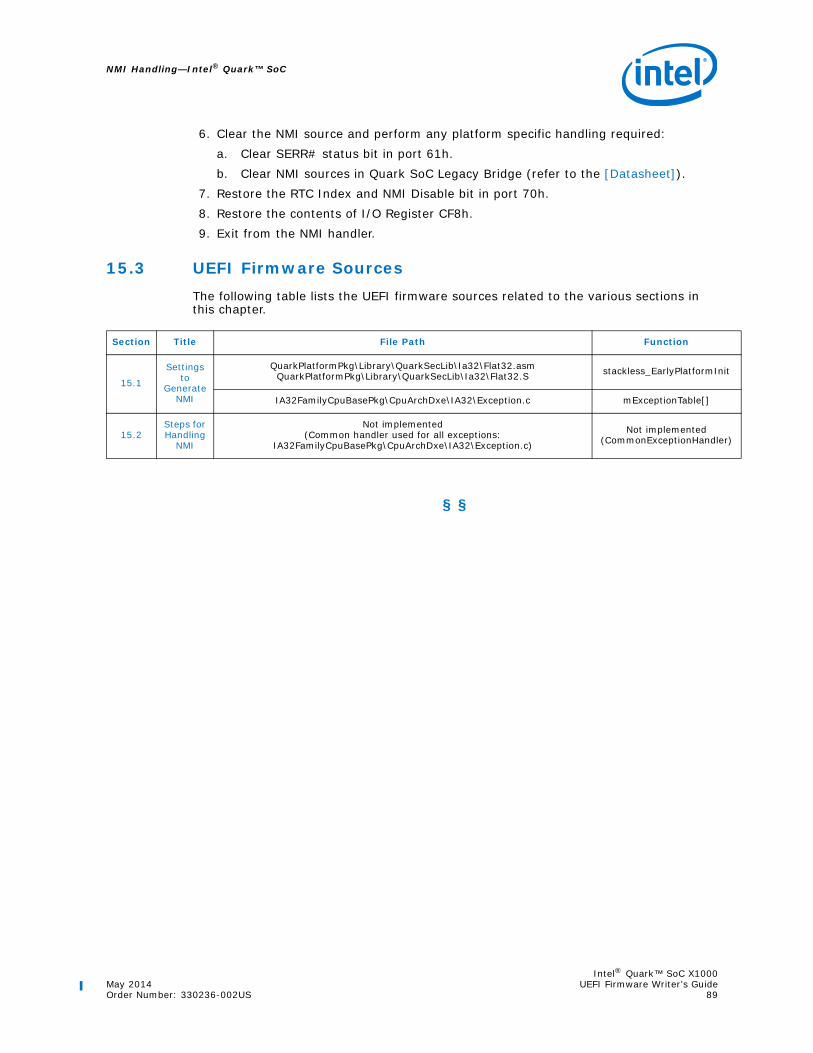
Intel® Quark™ SoC X1000May 2014 UEFI Firmware Writer’s GuideOrder Number: 330236-002US 89
NMI Handling—Intel® Quark™ SoC
6. Clear the NMI source and perform any platform specific handling required:a. Clear SERR# status bit in port 61h.b. Clear NMI sources in Quark SoC Legacy Bridge (refer to the [Datasheet]).
7. Restore the RTC Index and NMI Disable bit in port 70h.8. Restore the contents of I/O Register CF8h.9. Exit from the NMI handler.
15.3 UEFI Firmware SourcesThe following table lists the UEFI firmware sources related to the various sections in this chapter.
§ §
Section Title File Path Function
15.1
Settings to
Generate NMI
QuarkPlatformPkg\Library\QuarkSecLib\Ia32\Flat32.asmQuarkPlatformPkg\Library\QuarkSecLib\Ia32\Flat32.S stackless_EarlyPlatformInit
IA32FamilyCpuBasePkg\CpuArchDxe\IA32\Exception.c mExceptionTable[]
15.2Steps for Handling
NMI
Not implemented(Common handler used for all exceptions:
IA32FamilyCpuBasePkg\CpuArchDxe\IA32\Exception.c)
Not implemented(CommonExceptionHandler)

Intel® Quark™ SoC—SMI Handling
Intel® Quark™ SoC X1000UEFI Firmware Writer’s Guide May 201490 Order Number: 330236-002US
16.0 SMI Handling
The Quark SoC supports several sources of SMI. These include but are not limited to:• Legacy GPIOs• General Purpose Events (GPEs)• Inter Processor Interrupts (IPIs)• Power Management events
Please refer to the [Datasheet] for a full list of all possible sources of SMIs. UEFI firmware must provide support for configuring and handling any source of SMI required (platform specific design).
16.1 SMI on Sleep EnableThe enable SMI on sleep bit (GPE0BASE + 10h[2]) allows firmware to enable generation of an SMI when the operating system writes to the SLP_EN. The SMI on sleep status bit (GPE0BASE + 14h[2]) reflects the source of the SMI as the Sleep SMI.
In the handler for this event, firmware typically initiates workarounds that must be in place before entry into a sleep state. Examples include saving platform specific registers that need to be restored after a WAKE, changing the state of a GPIO, etc.
16.2 Setting the EOS BitSetting the EOS bit (GPE0BASE + 14[31]) will de-assert the SMI# signal and will re-arm SMIs. If there is a pending and enabled SMI status bit, the EOS bit will read back as cleared. In this case, a SMI will occur as soon as the resume instruction is executed.
16.3 SMI Status BitsThe SMI status bits must be cleared by software after the SMI source has been de-asserted. It is up to the SMI handler to de-assert the SMI source and clear the status bits. Status bits that are set for SMI sources can be set even if they are not enabled and do not need to be serviced or cleared. SMI Status bits should be qualified with their respective enables before being serviced. If enabled status bits are not cleared, the EOS bit will remain set.
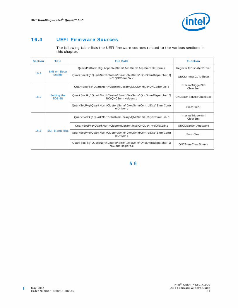
Intel® Quark™ SoC X1000May 2014 UEFI Firmware Writer’s GuideOrder Number: 330236-002US 91
SMI Handling—Intel® Quark™ SoC
16.4 UEFI Firmware SourcesThe following table lists the UEFI firmware sources related to the various sections in this chapter.
§ §
Section Title File Path Function
16.1 SMI on Sleep Enable
QuarkPlatformPkg\Acpi\DxeSmm\AcpiSmm\AcpiSmmPlatform.c RegisterToDispatchDriver
QuarkSocPkg\QuarkNorthCluster\Smm\DxeSmm\QncSmmDispatcher\QNC\QNCSmmSx.c QNCSmmSxGoToSleep
16.2 Setting the EOS Bit
QuarkSocPkg\QuarkNorthCluster\Library\QNCSmmLib\QNCSmmLib.c InternalTriggerSmiClearSmi
QuarkSocPkg\QuarkNorthCluster\Smm\DxeSmm\QncSmmDispatcher\QNC\QNCSmmHelpers.c QNCSmmSetAndCheckEos
QuarkSocPkg\QuarkNorthCluster\Smm\Dxe\SmmControlDxe\SmmControlDriver.c SmmClear
16.3 SMI Status Bits
QuarkSocPkg\QuarkNorthCluster\Library\QNCSmmLib\QNCSmmLib.c InternalTriggerSmiClearSmi
QuarkSocPkg\QuarkNorthCluster\Library\IntelQNCLib\IntelQNCLib.c QNCClearSmiAndWake
QuarkSocPkg\QuarkNorthCluster\Smm\Dxe\SmmControlDxe\SmmControlDriver.c SmmClear
QuarkSocPkg\QuarkNorthCluster\Smm\DxeSmm\QncSmmDispatcher\QNCSmmHelpers.c QNCSmmClearSource

Intel® Quark™ SoC—Power Management
Intel® Quark™ SoC X1000UEFI Firmware Writer’s Guide May 201492 Order Number: 330236-002US
17.0 Power Management
17.1 Power Button OverrideThe power button override is handled by the Quark SoC.
Note: There is no status register to indicate this event.
17.2 Power Failure ConsiderationsFirmware can detect a power failure by reading the DRAMI bit (GPE0BASE + 2Ch[0]). This bit could be set by the memory initialization code and is only cleared on a system power failure. So, if the bit is set the system is in the process of warm booting. If clear, the system is recovering from a power failure.
17.3 Processor ThrottlingQuark SoC does not support processor throttling. Only 100% duty cycle is supported. (P_BLK + 0h).
17.4 C StatesThe core provides support for C0, C1, and C2.
17.4.1 IRQ Break Events for C1 State
The C1 state is entered when the core executes a Halt (HLT) instruction.
IRQs are used as break events from a C1 state. If IRQs as break events must be disabled, firmware should do so using the 8259 mask registers prior to entering the C1 state. Firmware must also ensure that the mask register is enabled for the desired break events.
17.4.2 C2 State Support
C2 state support is available within the CPU. The C2 state is entered via reading the P_LVL2 register (P_BLK + 4h).
17.4.3 Cx State Support Reporting for ACPI OS
ACPI capable operating systems can support the C2 state by using the _CST control method implemented by system firmware. The example given below in Figure 7 assumes P_BLK address of 410h.

Intel® Quark™ SoC X1000May 2014 UEFI Firmware Writer’s GuideOrder Number: 330236-002US 93
Power Management—Intel® Quark™ SoC
17.4.4 Break Events
Break events cause the Quark SoC to transition from C2 back to C0, following the entry steps in reverse order. The break events for exiting from C2 state are:
• Any unmasked interrupt going active• Any internal event that causes an NMI or SMI#• Any internal event that causes INIT# to go active• A pending CPU break event, indicated by PBE#.
17.5 Wake EventsThe following events are capable of generating a wakeup from S4/S5:
• POWER/RESET BUTTON: Note: There is no status register to indicate this wake event.
The following events are capable of generating a wakeup from a suspend state (S3):• POWER/RESET BUTTON:
Note: There is no status register to indicate this wake event.• RTC ALARM: (RTC Enable at PM1BLK + 02h[10])• PCI Express* Devices: (PCI Express* enable at GPE0BASE + 04h[17]). These are
PCIe devices behind the PCIe Root Ports 0/1.• Legacy (resume well) GPIO: (GPIO enable at GPE0BASE + 04h[14] to globally
enable GPIO wake)• External General Purpose Event: (EGPE enable at GPE0BASE + 04h[13] to globally
enable EGPE wake)
UEFI firmware must configure/handle any of the above wake event required in the platform (platform design dependent). Please refer to the [Datasheet] for details of the above registers.
Figure 7. Cx State Support Reporting Through _CST Control Method
Processor (\_SB.CPU), //Processor Name1, //ACPI Processor number0x410,, //PBlk system IO address6 ) //PBlkLen{Method (_CST, 0){
Return ( Package () {3,Package() {ResourceTemplate() {Register(FFixedHW, 0 0 0)}, 1,
1, 1000},Package() {ResourceTemplate() {Register(SystemIO, 8, 0,
0x414)}, 2, 1, 500},})
}

Intel® Quark™ SoC—Power Management
Intel® Quark™ SoC X1000UEFI Firmware Writer’s Guide May 201494 Order Number: 330236-002US
17.6 UEFI Firmware SourcesThe following table lists the UEFI firmware sources related to the various sections in this chapter.
§ §
Section Title File Path Function
17.2 Power Failure Considerations QuarkPlatformPkg\Platform\Pei\PlatformInit\MrcWrapper.c MemoryInit
17.3 Processor Throttling
QuarkPlatformPkg\Acpi\AcpiTables\Cpu0Tst\Cpu0Tst.asl *.*
17.4 C States QuarkPlatformPkg\Acpi\AcpiTables\Cpu0Cst\Cpu0Cst.asl *.*
17.5 Wake Events
QuarkPlatformPkg\Acpi\AcpiTables\Dsdt\Platform.asl Scope(\_GPE)
QuarkSocPkg\QuarkNorthCluster\Library\IntelQNCLib\IntelQNCLib.c
QNCCheckS3AndClearStateQNCCheckPowerOnResetAndClearStat
e
QuarkPlatformPkg\Acpi\DxeSmm\AcpiSmm\AcpiSmmPlatform.c SxSleepEntryCallBack

Intel® Quark™ SoC X1000May 2014 UEFI Firmware Writer’s GuideOrder Number: 330236-002US 95
Suspend Handler Considerations—Intel® Quark™ SoC
18.0 Suspend Handler Considerations
18.1 Power-On Suspend Handling PreparationSuspend handling preparation occurs during initial system boot (that is, for EDKII boot modes BOOT_WITH_FULL_CONFIGURATION and BOOT_WITH_MINIMAL_CONFIGURATION) and is performed by the AcpiSmmPlatform.efi driver, as well as miscellaneous chipset drivers using the S3BootScriptLib library to save register setting they wish to be restored during S3 Resume.
18.2 S3 Entry Steps1. The ACPI operating system performs the steps "Transitioning from the Working to
the Sleeping State" in the ACPI Specification (Table 3).2. Step 1 above results in an SMI been generated and a generic QuarkSocPkg routine
QNCSmmCoreDispatcher being entered.3. QNCSmmCoreDispatcher determines a Sleep SMI has occurred and passes control
to the registered platform sleep handler SxSleepEntryCallBack.4. SxSleepEntryCallBack will:
a. Will save current runtime state of specific chipset registers so that they can be restored on resume (SaveRuntimeScriptTable).
b. Enable wake events, see Section 17.5.c. Assert PCI Express* signal PERST# to put PCIe cards into reset.
5. Control will return to QNCSmmCoreDispatcher which will Initiate Sleep States via SLP_EN Bit (QNCSmmSxGoToSleep, see Section 18.2.1).
18.2.1 Initiating Sleep States via SLP_EN Bit
Before the software sets SLP_EN bit in PM1_CNT register (PM1_BLK+04h[13]), interrupts must be masked and bus master activity must be disabled.
In an ACPI OS environment, the operating system is expected to ensure that this requirement is met.
If firmware sets the SLP_EN bit, it becomes the responsibility of firmware to ensure that the above requirement is met.
18.3 S3 Resume StepsFirmware executes the following generic steps when resuming a system from S3 state (Suspend to RAM).
On a resume from S3 state the Quark SoC starts executing from the reset vector location of FFFF_FFF0h.

Intel® Quark™ SoC—Suspend Handler Considerations
Intel® Quark™ SoC X1000UEFI Firmware Writer’s Guide May 201496 Order Number: 330236-002US
1. Re-program all chipset-specific base address registers, as described in Table 11 and Table 12.
2. Verify the system is waking (PM1_BLK + 00h[15]) and that the system is resuming from S3 state by looking at the SLP_TYP bit field (PM1_BLK + 04h[12:10]). If the system is not resuming from S3 state do not execute any of the steps below.
3. The system firmware will execute the steps for getting the memory functional in the platform and continue with the rest of the steps required for a system-wide resume.
4. Restore the Quark SoC configuration:a. Any SOC configuration perform by Intel® Quark™ SoC PEI stage drivers.b. Relocate the SMM base address to the SMM base that is being used in the
system.c. Initialize the cache. This will involve the restore of the MTRR registers in the
Quark SoC.5. Restore Chipset registers saved using s3BootScriptLib and
SaveRuntimeScriptTable. 6. If the system is resuming back to an ACPI OS the control can be passed to the ACPI
OS waking vector at this step. An ACPI OS may reassign the PCI registers to some other value than what the firmware assigned in step 5. Step 5 is required as a safety step where the PCI devices have a default Base address register value assigned if a problem arises.
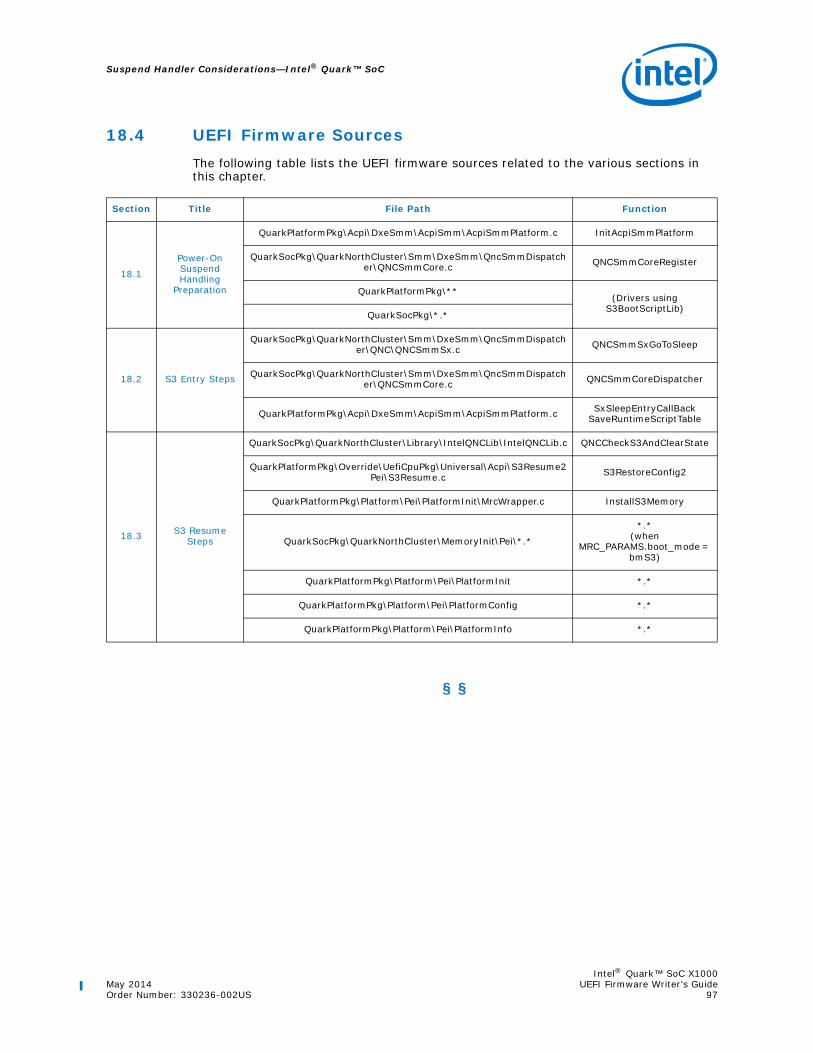
Intel® Quark™ SoC X1000May 2014 UEFI Firmware Writer’s GuideOrder Number: 330236-002US 97
Suspend Handler Considerations—Intel® Quark™ SoC
18.4 UEFI Firmware SourcesThe following table lists the UEFI firmware sources related to the various sections in this chapter.
§ §
Section Title File Path Function
18.1
Power-On Suspend Handling
Preparation
QuarkPlatformPkg\Acpi\DxeSmm\AcpiSmm\AcpiSmmPlatform.c InitAcpiSmmPlatform
QuarkSocPkg\QuarkNorthCluster\Smm\DxeSmm\QncSmmDispatcher\QNCSmmCore.c QNCSmmCoreRegister
QuarkPlatformPkg\**(Drivers using
S3BootScriptLib)QuarkSocPkg\*.*
18.2 S3 Entry Steps
QuarkSocPkg\QuarkNorthCluster\Smm\DxeSmm\QncSmmDispatcher\QNC\QNCSmmSx.c QNCSmmSxGoToSleep
QuarkSocPkg\QuarkNorthCluster\Smm\DxeSmm\QncSmmDispatcher\QNCSmmCore.c QNCSmmCoreDispatcher
QuarkPlatformPkg\Acpi\DxeSmm\AcpiSmm\AcpiSmmPlatform.c SxSleepEntryCallBackSaveRuntimeScriptTable
18.3 S3 Resume Steps
QuarkSocPkg\QuarkNorthCluster\Library\IntelQNCLib\IntelQNCLib.c QNCCheckS3AndClearState
QuarkPlatformPkg\Override\UefiCpuPkg\Universal\Acpi\S3Resume2Pei\S3Resume.c S3RestoreConfig2
QuarkPlatformPkg\Platform\Pei\PlatformInit\MrcWrapper.c InstallS3Memory
QuarkSocPkg\QuarkNorthCluster\MemoryInit\Pei\*.*
*.*(when
MRC_PARAMS.boot_mode = bmS3)
QuarkPlatformPkg\Platform\Pei\PlatformInit *.*
QuarkPlatformPkg\Platform\Pei\PlatformConfig *.*
QuarkPlatformPkg\Platform\Pei\PlatformInfo *.*

Intel® Quark™ SoC—High Performance Event Timer (HPET) Support
Intel® Quark™ SoC X1000UEFI Firmware Writer’s Guide May 201498 Order Number: 330236-002US
19.0 High Performance Event Timer (HPET) Support
19.1 HPET Basic ConfigurationThe address of the HPET register block in the Quark SoC is always mapped to address FED00000h. No programming is required to enable decoding of this region. In all other respects, the operation and programming of the HPET is identical to previous platforms.
UEFI firmware is responsible for reporting the presence of the HPET and the resources it consumes to the OS via ACPI tables.
For additional details, refer to the [Datasheet], in the Legacy Bridge HPET Registers section. Also refer to the ACPI specification for additional details on reporting the HPET to the OS.
19.2 UEFI Firmware SourcesThe following table lists the UEFI firmware sources related to the various sections in this chapter.
§ §
Section Title File Path Function
19.1 HPET Basic Configuration
QuarkPlatformPkg\Acpi\Dxe\AcpiPlatform\AcpiPlatform.c AcpiUpdateTableAcpiPlatformEntryPoint
QuarkPlatformPkg\Acpi\AcpiTables\Dsdt\LpcDev.asi Device(HPET)
QuarkPlatformPkg\Acpi\AcpiTables\Hpet\Hpet.aslc *.*

Intel® Quark™ SoC X1000May 2014 UEFI Firmware Writer’s GuideOrder Number: 330236-002US 99
GPIO Handling—Intel® Quark™ SoC
20.0 GPIO Handling
20.1 Legacy GPIOsThe Quark SoC supports two core well legacy GPIOs and six resume well legacy GPIOs. Each GPIO is capable of input, output, SCI generation, SMI generation, and NMI generation. Also, when configured as inputs, each GPIO can generate an interrupt on the rising and/or the falling edge of the input signal. Resume well GPIOs are also capable of generating WAKE events (refer to Section 17.5).
20.1.1 Legacy GPIO Configuration
The offset and function of the GPIO registers is given below. The GPIOs should be configured to match the associated functionality on the platform.
Note: Two core well and six resume well GPIOs are present in the legacy block. So only bits 1:0 are valid for the core well GPIO registers and 5:0 for resume well GPIO registers.
Note: The offsets given below are from the GPIO Base Address, as programmed in D31:F0:R44h. See Table 11, “Non-Standard IO Base Address Registers” on page 24 for details.
20.1.2 Legacy GPIO Interrupt Handling
If a GPIO is configured to generate an interrupt, in the GPIO interrupt handler software must:1. Check the GPIO status bit in the GPE0 status register (GPE0_BLK base + 0h[14]) if
in a GPE handler and the SMI status register (GPE0_BLK base + 14h[9]) if in the SMI handler.
2. If the GPIO status bit is set, software must determine which GPIO caused the interrupt by reading the core and resume well “Trigger Status” registers.
3. Handle any GPIOs whose associated status bits are set.
Table 40. GPIO Registers Offset and Function
Core Well GPIO Offset Resume Well GPIO Offset Function
0000h 0020h Enable
0004h 0024h I/O Select (0=Output, 1=Input)
0008h 0028h Level
000Ch 002Ch Positive Edge Trigger Enable
0010h 0030h Negative Edge Trigger Enable
0014h 0034h GPE Enable
0018h 0038h SMI Enable
001Ch 003Ch Trigger Status
0040h 0044h NMI Enable

Intel® Quark™ SoC—GPIO Handling
Intel® Quark™ SoC X1000UEFI Firmware Writer’s Guide May 2014100 Order Number: 330236-002US
4. Clear the status bits in the “Trigger Status” register (GPIO Base + 1Ch/3Ch for core/resume well GPIOs).
5. Clear the GPIO GPE or SMI status bit in the GPE0_BLK (GPE0_BLK base + 0h[14] for a GPE or GPE0_BLK base + 14h[9] for an SMI).
20.2 Chipset South Cluster GPIO ControllerThe Quark SoC supports 8 Independently configurable GPIOs, Separate data register and data direction for each GPIO, Interrupt source mode supported for each GPIO, De-bounce logic for interrupt sources and Metastability registers for GPIO read data
20.2.1 South Cluster GPIO Controller Configuration
The GPIO MMIO register are shown below. The GPIOs should be initially configured after PCI Enumeration to match the associated functionality on the platform.
20.3 UEFI Firmware SourcesThe following table lists the UEFI firmware sources related to the various sections in this chapter.
Table 41. South Cluster GPIO Controller MMIO Registers
MMIO Address Function
I2C/GPIO Controller [BAR1] + 00h[7:0]BAR1 Reference: [B:0, D:21, F:2] + 14h
GPIO Port A data bits (GPIO_SWPORTA_DR)
I2C/GPIO Controller [BAR1] + 04h[7:0]BAR1 Reference: [B:0, D:21, F:2] + 14h
GPIO Port A data direction bits (GPIO_SWPORTA_DDR)
I2C/GPIO Controller [BAR1] + 30h[7:0]BAR1 Reference: [B:0, D:21, F:2] + 14h
Interrupt Enable (GPIO_INTEN)
I2C/GPIO Controller [BAR1] + 34h[7:0]BAR1 Reference: [B:0, D:21, F:2] + 14h
Interrupt Mask (GPIO_INTMASK)
I2C/GPIO Controller [BAR1] + 38h[7:0]BAR1 Reference: [B:0, D:21, F:2] + 14h
Interrupt Type (GPIO_INTTYPE_LEVEL)
I2C/GPIO Controller [BAR1] + 3Ch[7:0]BAR1 Reference: [B:0, D:21, F:2] + 14h
Interrupt Polarity (GPIO_INT_POLARITY)
I2C/GPIO Controller [BAR1] + 48h[7:0]BAR1 Reference: [B:0, D:21, F:2] + 14h
Debounce Enable (GPIO_DEBOUNCE)
I2C/GPIO Controller [BAR1] + 60h[0]BAR1 Reference: [B:0, D:21, F:2] + 14h
Synchronization Level (GPIO_LS_SYNC)
Section Title File Path Functions/Tables
20.1.1 Legacy GPIO Configuration
QuarkPlatformPkg\Platform\Pei\PlatformInit\PlatformEarlyInit.cEarlyPlatformGpioInit
EarlyPlatformGpioManipulation
QuarkPlatformPkg\Include\PlatformBoards.h PLATFORM_LEGACY_GPIO_TABLE_DEFINITION

Intel® Quark™ SoC X1000May 2014 UEFI Firmware Writer’s GuideOrder Number: 330236-002US 101
GPIO Handling—Intel® Quark™ SoC
§ §
20.1.2 Legacy GPIO Interrupt Handling
Not implemented(Intel® Quark™ SoC not supporting legacy GPIO interrupts in UEFI
firmware)
Not implemented(Intel® Quark™ SoC not supporting legacy GPIO
interrupts in UEFI firmware)
20.2.1South Cluster
GPIO Controller Configuration
QuarkPlatformPkg\Platform\Dxe\PlatformInit\PlatformConfig.c GpioControllerConfigPlatformResetDevices
QuarkPlatformPkg\Include\PlatformBoards.h PLATFORM_GPIO_CONTROLLER_CONFIG_DEFINITION
Section Title File Path Functions/Tables

Intel® Quark™ SoC—Security Enhancements
Intel® Quark™ SoC X1000UEFI Firmware Writer’s Guide May 2014102 Order Number: 330236-002US
21.0 Security Enhancements
21.1 IntroductionThis chapter is dedicated to describing the enhancements made to the Intel® Quark™ SoC UEFI firmware to make it more robust and resistant to attacks and failures. These enhancements are designed to reduce the risk of a system becoming non-bootable or compromised.
21.1.1 Security Build Options
Some of the following sections have different levels of Security depending on the build options used to generate the firmware images. For details, see [Build Guide].
Security Build Options:• NONE
No security build options specified in EDKII build parameters• -DSECURE_LD
Secure Lockdown build option specified in EDKII build parameters
21.2 Secure BootFor Intel Intel® Quark™ SoC X1000 secure SKU, the hardware implements a root of trust that starts executing code from ROM at the reset vector (0xFFFFFFF0). This ROM code authenticates the Intel® Quark™ SoC UEFI firmware before passing control to it. The ROM code will not launch Intel® Quark™ SoC UEFI firmware if it fails authentication.
Intel® Quark™ SoC UEFI firmware is split into two firmware volumes:• Stage1 Firmware Volume • Stage2 Firmware Volume
The Stage1 Firmware Volume continues the chain of trust by first authenticating the Stage2 Firmware Volume (via a call to the ROM code to perform the authentication) before passing control to it. This chain of trust is continued all the way up to the OS. For a detailed description of the Intel® Quark™ SoC secure boot feature, see [Secure Boot].
There is a security key module stored in flash (see [Secure Boot]). Intel® Quark™ SoC UEFI firmware always validates this key module before it validates Stage2 Firmware volumes and firmware update capsules (see Figure 8). The firmware may or may not also validate the key module for other images (for example, bootloader payload). See the QuarkBootRomLib (Section 21.12) for details.

Intel® Quark™ SoC X1000May 2014 UEFI Firmware Writer’s GuideOrder Number: 330236-002US 103
Security Enhancements—Intel® Quark™ SoC
21.2.1 Secure Boot Simulation on Base SKU Hardware
For base SKU hardware, also called non-secure SKU, the ROM Secure Boot Authentication Functions (see [Secure Boot]) are implemented in the EDKII_BOOTROM_OVERRIDE (see EDKII platform .fdf build file) firmware volume. The simulation routines always return a positive result.
21.3 Isolated Memory Regions (IMRs)Intel® Quark™ SoC hardware provides the capability to configure IMRs to allow/deny access by certain system agents to programmed memory ranges. Thus, an area of memory that is only for use by the host processor can be protected from other DMA agents in the system. Intel® Quark™ SoC UEFI firmware uses IMRs to protect the following sensitive assets during boot:
• PeiMemory: Memory used for Intel® Quark™ SoC UEFI firmware code/data, boottime services code/data, stack, OS loader
• ACPI Memory: Memory that holds ACPI reclaim, runtime services code/data, reserved memory, ACPI NVS memory
• RMU Memory: RMU binary in memory• Legacy S3 Memory: Region of memory below 1MB that hold legacy S3 code• AP Startup Vector Memory: Region of memory that is used for startup code for
multi-processor capable systems• Default SMRAM Memory: Region of memory that SMRAM is mapped to following a
processor reset (typically used to relocate the SMBASE to TSEG).• eSRAM Memory: Memory that the initial Stage1 Firmware Volume is copied into
(from legacy SPI flash) following a system reset.
IMRs that must persist even after OS boot are locked by Intel® Quark™ SoC UEFI firmware. The following table shows when IMRs must be set up and torn down for each of the above memory regions:
Similar to the Intel® Quark™ SoC UEFI firmware, the OS loader/OS must also use IMRs to protect sensitive assets it uses. This involves destroying/re-allocation IMRs that were set up by Intel® Quark™ SoC UEFI firmware but that are no longer required (for example, after the OS call to ’ExitBootServices’, the PeiMemory/AP Startup Vector Memory is available to the OS so it must remove the IMRs that were created for those
Table 42. Create/Destroy/Lock Requirements for IMRs
Memory Region IMR Create IMR Destroy IMR Lock
eSRAM Reset Vector code Stage2 Firmware Volume No
PeiMemory Stage1 Firmware Volume (Normal boot path)
OS (after ExitBootServices and OS loader has transferred control to the OS) No
ACPI Memory Stage1 Firmware Volume (Normal boot path) No Yes
RMU Memory Stage1 Firmware Volume (Normal boot path) Stage2 Firmware Volume No
Legacy S3 Memory
Stage1 Firmware Volume (Normal boot path) No Yes
AP Startup Vector Memory
Stage1 Firmware Volume (Normal boot path) OS (after ExitBootServices) No
Default SMRAM Memory
Stage1 Firmware Volume (Normal boot path) Stage2 Firmware Volume No

Intel® Quark™ SoC—Security Enhancements
Intel® Quark™ SoC X1000UEFI Firmware Writer’s Guide May 2014104 Order Number: 330236-002US
regions). In addition, the OS must be aware that any IMRs locked by Intel® Quark™ SoC UEFI firmware are not available to the OS (ACPI Memory and Legacy S3 Memory IMRs).
Thus, IMR design is done at a system level where Reset Vector Code/Intel® Quark™ SoC UEFI Firmware/OS Loader/OS must all agree on IMR implementation and usage. It is not supported to have IMRs implemented by only some of those components. IMRs are either implemented by all components in the system or none at all. For IMR design details, refer to [Secure Boot].
21.4 Legacy SPI Flash ProtectionFor all boot modes except BOOT_ON_FLASH_UPDATE (no matter what build options was used to build the firmware) Legacy SPI Flash Range Protection is enabled (see Section 21.4.1.1 and Section 21.4.2.1) and the configuration registers (see Section 10.5) of the Legacy SPI Flash controller are locked. This happens early in the PI DXE stage before PCI enumeration when SMM SPI initialization has completed. For BOOT_ON_FLASH_UPDATE boot mode at this point, the Legacy SPI Flash Range Protection is enabled, but the configuration registers are not locked. Later, before flash is programmed for boot mode, BOOT_ON_FLASH_UPDATE Legacy SPI Flash Range Protection is disabled.
Depending on Security Build options used to build the firmware, runtime restrictions of who can update a SPI Legacy Flash area and if a SPI Legacy flash area is writable are applied to legacy SPI Flash.
21.4.1 No Security Build options used to build firmware
21.4.1.1 Legacy SPI Flash Range Protection
The following ranges are protected using SPI range protection registers (see Section 10.3) just before the EDKII Boot manager loads and starts the initial Boot option:
• Platform Data Area. The Base Address and Length of this protected region is defined by the EDKII PCDs PcdPlatformDataBaseAddress and PcdPlatformDataMaxLen. For details, see the Intel® Quark™ SoC X1000 Board Support Package (BSP) Build and Software User Guide [Build Guide].
• Fixed Recovery Stage1 image. The Base Address and Length of this protected region is defined by the EDKII PCDs PcdFlashFvFixedStage1AreaBase and PcdFlashFvFixedStage1AreaSize.
• Boot ROM override image. Located in the last logical area at the end of system flash. See EDKII_BOOTROM_OVERRIDE references in EDKII platform .fdf build file for the size of this area at the end of flash.
21.4.1.2 Legacy SPI Flash Update Protection
All SPI Flash regions not protected by SPI range protection registers (see Section 10.3) are writable by run-time code.
21.4.2 Secure Lock Down build (-DSECURE_LD) used to build firmware
For this build option Intel® Quark™ SoC UEFI firmware (capsule mechanism) is the only mechanism allowed to update/recover the legacy SPI flash. In addition, Intel® Quark™ SoC UEFI firmware is the only module allowed to update the legacy SPI flash

Intel® Quark™ SoC X1000May 2014 UEFI Firmware Writer’s GuideOrder Number: 330236-002US 105
Security Enhancements—Intel® Quark™ SoC
NVRAM area where UEFI EFI_VARIABLE_NON_VOLATILE variables are stored. To enforce this, Intel® Quark™ SoC UEFI firmware implements SPI flash protection as follows.
21.4.2.1 Legacy SPI Flash Range Protection
Intel® Quark™ SoC UEFI firmware write protects all SPI Flash except for the NVRAM area (where runtime UEFI EFI_VARIABLE_NON_VOLATILE variables are stored) just before the EDKII Boot manager loads and starts the initial Boot option. This point in time is after the firmware has determined that capsule update is not required. Write protection is achieved using SPI range protection registers (see Section 10.3).
21.4.2.2 Legacy SPI Flash Update Protection
Intel® Quark™ SoC UEFI firmware is the only module allowed to update the legacy SPI flash NVRAM area where UEFI EFI_VARIABLE_NON_VOLATILE variables are stored. However, the legacy SPI flash NVRAM area cannot be protected as in Section 21.4.2.1 because this area may be updated during Intel® Quark™ SoC UEFI firmware boot and also at runtime (UEFI runtime variable support). To enforce the policy of Intel® Quark™ SoC UEFI firmware being the only module allowed to update this area, the legacy SPI flash controller is configured to generate an SMI on any attempt to write to the legacy SPI flash. This protection mechanism is enabled just after the SMI access violation handler has been registered. Refer to Section 10.6 for the legacy SPI controller registers used to implement this legacy SPI flash update protection mechanism.
The SMI handler will not enable flash writes but instead increments an access violation count variable which is stored as an UEFI NVRAM variable. On every boot, if the handler finds the count is not equal to zero, it will trace the value of the count to the console and clear the count variable. No security decisions are taken on the value of the count, but it is useful for debug during bootloader and operating system integration testing.
21.5 PCIe Option ROMsDepending on Security Build options used to build the firmware, a boot time restriction on loading PCIe Option ROMs is applied.
21.5.1 No Security Build options used to build firmware
All PCIe Option ROM Load requests are allowed.
21.5.2 Secure Lock Down build (-DSECURE_LD) used to build firmware
Intel® Quark™ SoC UEFI firmware will not load PCIe Option ROMs from any plug in PCIe cards. Instead, any option ROMs required will be built into the Intel® Quark™ SoC UEFI firmware image. This is typical for embedded systems where the onboard firmware is capable of initializing any hardware it needs.
21.6 Register LockingCertain Quark SoC registers are responsible for setting up critical system operating features. Once set up, these registers can be locked to prevent malicious changing of their settings to compromise or hang the system. Intel® Quark™ SoC UEFI firmware locks the following critical registers for security (a reset is required to unlock) no matter what build options are used to build the firmware:
• HMBOUND (Op codes 10h/11h: Msg Port 03h: R08h): Determines if a memory access is routed to the MSS or to MMIO. This register is locked after DDR3 initialization is complete when the top of physical memory is known. Refer to

Intel® Quark™ SoC—Security Enhancements
Intel® Quark™ SoC X1000UEFI Firmware Writer’s Guide May 2014106 Order Number: 330236-002US
Section 4.1.• HSMMCTL (Op codes 10h/11h: Msg Port 03h: R04h): Defines where in the address
space SMRAM is located and allows memory reads/writes to this range to be blocked when not in SMM mode. This register is locked after SMM initialization is complete. Refer to Section 4.4.2.
• IMRxL (Op codes 10h/11h: Msg Port 05h: R1x0h [x=0 to 7]): Intel® Quark™ SoC UEFI firmware locks any IMR that must persist through OS boot and beyond. Refer to Section 21.3.
• Thermal Configuration registers. Refer to Table 14.• Legacy SPI Controller configuration registers. Refer to Section 10.5.
21.6.1 Secure Lock Down build (-DSECURE_LD) used to build firmware
Intel® Quark™ SoC UEFI firmware locks the following additional registers if the build option -DSECURE_LD is used to build the firmware.
• Lock Remote Management DMA (Set to 1b Bit0 of Op codes 10h/11h: Msg Port 04h:R72h)
21.7 Redundant ImagesIt is important that corrupt legacy SPI flash images or legacy SPI flash images that fail to authenticate (secure SKU) should not leave the system un-recoverable. Intel® Quark™ SoC UEFI firmware achieves this by providing redundant Stage1 Firmware Volumes as follows:
• Boot Stage1 Firmware Volume Image1 - This is the first Stage1 Firmware Volume• Boot Stage1 Firmware Volume Image2 - This is the redundant Stage1 Firmware
Volume• Fixed Recovery Firmware Volume Image - This is the fixed Recovery Firmware
Volume whose base and length is defined by the fixed EDKII PCDs PcdFlashFvFixedStage1AreaBase and PcdFlashFvFixedStage1AreaSize
The reset vector code (ROM code for secure SKU) will transfer control to the first ’good’ Firmware Volume found from the above list. If both Boot Stage1 Firmware Volumes are ’bad’ then the fixed Recovery Firmware Volume is launched. Only if all Firmware Volumes in the above list are ’bad’ will the system be un-recoverable. To reduce the risk of ending up with all Firmware Volumes corrupt, it is recommended that all Firmware Volumes above should not be updated in the one update. In reality, it is expected that the Fixed Recovery Firmware Volume will rarely need to be updated. The Fixed Recovery Firmware volume just needs to be ’good enough’ to recover the system and updates to it are only expected to address security vulnerabilities.
Failures of Stage2 and subsequent images will result in control being transferred to the Recovery Firmware Volume.
Refer to the [Secure Boot] for detailed description of this redundant images feature.
21.8 Limiting Boot Options
21.8.1 No Security Build options used to build firmware
No boot option limitations are enforced thus allowing the system to boot from all bootable media.

Intel® Quark™ SoC X1000May 2014 UEFI Firmware Writer’s GuideOrder Number: 330236-002US 107
Security Enhancements—Intel® Quark™ SoC
21.8.2 Secure Lock Down build (-DSECURE_LD) used to build firmware
Intel® Quark™ SoC UEFI firmware only supports booting an image (OS bootloader/UEFI application) from a known location in legacy SPI flash. This removes the risk of unknown UEFI applications/drivers being loaded from USB/SD/UEFI shell and causing unexpected system behavior or even compromising the system. For embedded systems, it is expected that the system will always boot from a known image at a known location (unlike personal computers and servers).
Note that the EDKII Boot manager is capable of booting images from other media (USB/SD/UEFI shell), but Intel® Quark™ SoC UEFI firmware restricts the boot manager from booting these images.
21.9 Denial of Service/Compromise Prevention
21.9.1 SMI Pin Blocking
Quark SoC provides the ability to disable the SMI pin, thus preventing the SMI signal reaching the processor. This could result in a denial of service in some cases (preventing the relocation of the SMBASE for example). In other cases, it could also result in the system being compromised. If, for security reasons, SMI trapping of certain events were set up, then this would prevent the UEFI firmware SMI handler from trapping these events and taking the appropriate action.
Intel® Quark™ SoC UEFI firmware makes sure the SMI pin is not masked by explicitly enabling it at the following stages during boot:
• Start of Stage1 Firmware Volume - Early boot code• SMM Exit - Just before executing the ’rsm’ instruction to exit SMM
21.10 Memory Training Engine LockdownAs part of DDR3 memory initialization code, the Intel® Quark™ SoC UEFI firmware makes use of a hardware engine to assist in the training of memory. Once DDR3 memory initialization is complete, Intel® Quark™ SoC UEFI firmware locks the hardware training engine to prevent further training sequences being initiated.
21.11 SMM Security Enhancements
21.11.1 SMRAM Caching
SMRAM caching is always disabled by hardware for the secure SKU regardless of the settings for the MTRRs/SMRR. This is to enhance SMM security due to caching issues. Intel® Quark™ SoC UEFI firmware sets up SMRAM as un-cached for the base SKU (non-secure) also to enhance its security.
As periodic SMIs are not used, SMI’s in general should be very infrequent. Thus, uncached SMRAM is not expected to have a major system performance impact.
21.11.2 SMBASE Relocation Address Selection
The address selected for SMBASE relocation should not overlap fixed Local APIC range (FEE00000h-FEEFFFFFh).
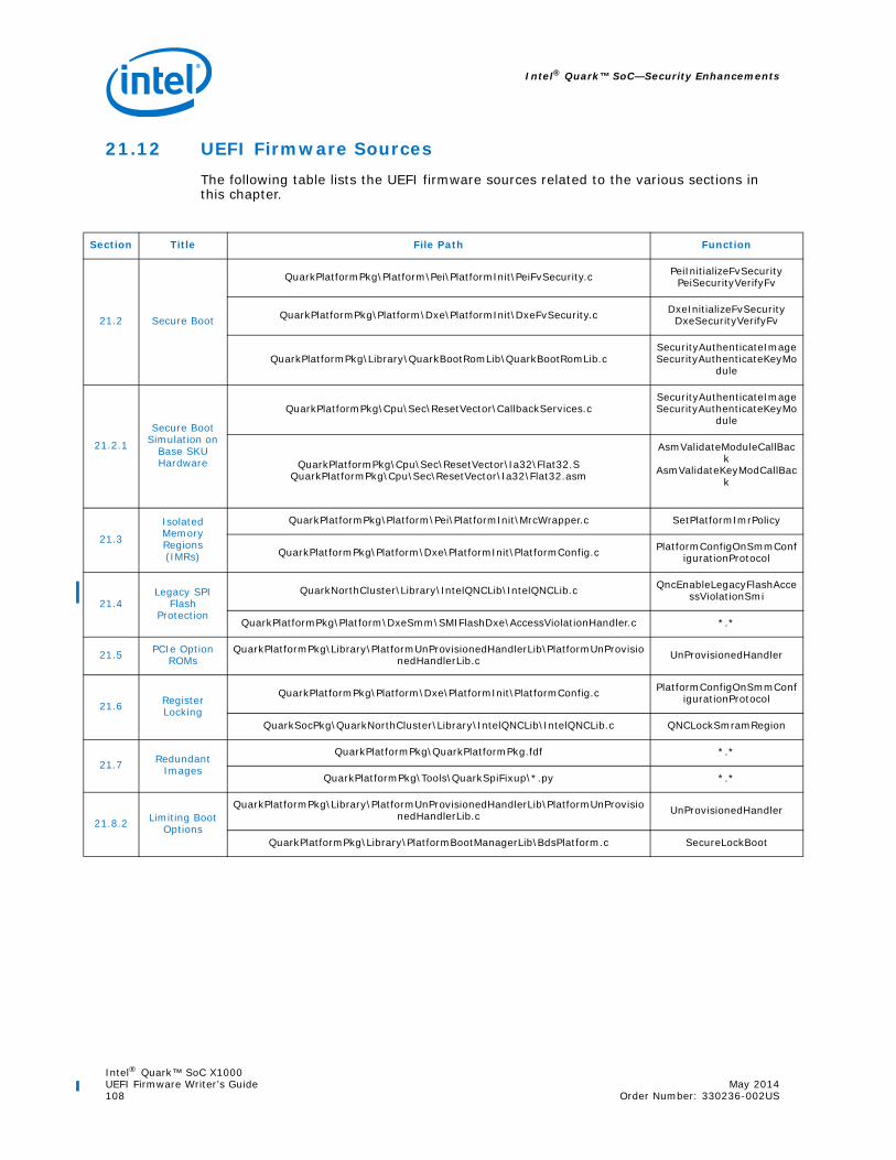
Intel® Quark™ SoC—Security Enhancements
Intel® Quark™ SoC X1000UEFI Firmware Writer’s Guide May 2014108 Order Number: 330236-002US
21.12 UEFI Firmware SourcesThe following table lists the UEFI firmware sources related to the various sections in this chapter.
Section Title File Path Function
21.2 Secure Boot
QuarkPlatformPkg\Platform\Pei\PlatformInit\PeiFvSecurity.c PeiInitializeFvSecurityPeiSecurityVerifyFv
QuarkPlatformPkg\Platform\Dxe\PlatformInit\DxeFvSecurity.c DxeInitializeFvSecurityDxeSecurityVerifyFv
QuarkPlatformPkg\Library\QuarkBootRomLib\QuarkBootRomLib.cSecurityAuthenticateImageSecurityAuthenticateKeyMo
dule
21.2.1
Secure Boot Simulation on
Base SKU Hardware
QuarkPlatformPkg\Cpu\Sec\ResetVector\CallbackServices.cSecurityAuthenticateImageSecurityAuthenticateKeyMo
dule
QuarkPlatformPkg\Cpu\Sec\ResetVector\Ia32\Flat32.SQuarkPlatformPkg\Cpu\Sec\ResetVector\Ia32\Flat32.asm
AsmValidateModuleCallBack
AsmValidateKeyModCallBack
21.3
Isolated Memory Regions (IMRs)
QuarkPlatformPkg\Platform\Pei\PlatformInit\MrcWrapper.c SetPlatformImrPolicy
QuarkPlatformPkg\Platform\Dxe\PlatformInit\PlatformConfig.c PlatformConfigOnSmmConfigurationProtocol
21.4Legacy SPI
Flash Protection
QuarkNorthCluster\Library\IntelQNCLib\IntelQNCLib.c QncEnableLegacyFlashAccessViolationSmi
QuarkPlatformPkg\Platform\DxeSmm\SMIFlashDxe\AccessViolationHandler.c *.*
21.5 PCIe Option ROMs
QuarkPlatformPkg\Library\PlatformUnProvisionedHandlerLib\PlatformUnProvisionedHandlerLib.c UnProvisionedHandler
21.6 Register Locking
QuarkPlatformPkg\Platform\Dxe\PlatformInit\PlatformConfig.c PlatformConfigOnSmmConfigurationProtocol
QuarkSocPkg\QuarkNorthCluster\Library\IntelQNCLib\IntelQNCLib.c QNCLockSmramRegion
21.7 Redundant Images
QuarkPlatformPkg\QuarkPlatformPkg.fdf *.*
QuarkPlatformPkg\Tools\QuarkSpiFixup\*.py *.*
21.8.2 Limiting Boot Options
QuarkPlatformPkg\Library\PlatformUnProvisionedHandlerLib\PlatformUnProvisionedHandlerLib.c UnProvisionedHandler
QuarkPlatformPkg\Library\PlatformBootManagerLib\BdsPlatform.c SecureLockBoot

Intel® Quark™ SoC X1000May 2014 UEFI Firmware Writer’s GuideOrder Number: 330236-002US 109
Security Enhancements—Intel® Quark™ SoC
§ §
21.9
Denial of Service/
Compromise Prevention
QuarkPlatformPkg\Library\SmmCpuPlatformHookLib\SmmCpuPlatformHookLib.c
PlatformSmmExitProcessing
QuarkPlatformPkg\Library\QuarkSecLib\Ia32\Flat32.asm
QuarkPlatformPkg\Library\QuarkSecLib\Ia32\Flat32.Sstackless_EarlyPlatformInit
21.10
Memory Training Engine
Lockdown
QuarkSocPkg\QuarkNorthCluster\MemoryInit\Pei\meminit.c lock_registers
21.11.2
SMBASE Relocation Address Selection
QuarkPlatformPkg\Platform\Pei\PlatformInit\MrcWrapper.c GetMemoryMap
Section Title File Path Function

Intel® Quark™ SoC—Firmware Update
Intel® Quark™ SoC X1000UEFI Firmware Writer’s Guide May 2014110 Order Number: 330236-002US
22.0 Firmware Update
22.1 IntroductionThis chapter describes how the Intel® Quark™ SoC UEFI firmware is updated during system runtime.
In brief, the firmware update involves:• Creating a firmware update capsule. The capsule has multiple images to be placed
at specified locations in the SPI flash (refer to Figure 8 and Section 22.2). The full capsule shown in Figure 8 would be contained in a single .cap file.
• Placing the .cap file in memory and calling the UEFI runtime service UpdateCapsule() with the memory location of the capsule. This is done by a runtime agent either running in an UEFI Shell or operating system.
• Programming the capsule images to flash immediately OR after a warm reset, depending on when UpdateCapsule() is called and the arguments that are passed.
• Calling the UEFI runtime service ResetSystem() if a warm reset is required. This service notices that a capsule is in memory and does an immediate S3 reset so that the capsule is preserved in memory after the reset.
• Processing the capsule and programming the capsule images into SPI flash.• Initiating a cold reset after SPI flash programming is complete to boot with the new
SPI flash images.
UpdateCapsule() is described in Section 7.5.3 of the UEFI Specifications (see Table 3) which allows passing information/capsules to the firmware. The format of the capsule passed to UpdateCapsule() is platform-specific.
Example images placed in capsule (Figure 8) would be PEI Stage1 images, DXE Stage2 Image, and EDKII NVRAM Image. A typical EDKII capsule is comprised of contiguous data starting at the Capsule Header Block. The Security Header Block shown in Figure 8 is Quark-specific. For information on the first Security Header Block shown in Figure 8, refer to sections on Asset Signing and Secure Boot Header Data Structures in [Secure Boot] with further information on signing files in the [Build Guide].
As noted above a reset may be required to update the firmware. Many of the following sub sections describe how the firmware update completes during the firmware boot flow after the reset.
22.1.1 UpdateCapsule() EDKII Module and Platform Module Dependencies
The UpdateCapsule() runtime service is implemented by the core EDKII driver CapsuleRuntimeDxe and depends on a platform implementation of EDKII library classes CapsuleLib to process the capsule it receives.

Intel® Quark™ SoC X1000May 2014 UEFI Firmware Writer’s GuideOrder Number: 330236-002US 111
Firmware Update—Intel® Quark™ SoC
If reset is required, then the following are also required: core EDKII driver ResetSystemRuntimeDxe, platform implementation of the EDKII library class ResetSystemLib, and core EDKII driver CapsulePei. After the reset to complete the firmware update, platform hooks in PEI stage call CapsulePei and in DXE stage they call CapsuleLib.
22.1.2 Intel® Quark™ SoC UEFI firmware update steps in detail:
1. Platform owner creates a capsule for Intel® Quark™ SoC UEFI firmware update (see Section 22.2) in firmware build environment.
2. A UEFI Application or Operating System application running on the target calls the UEFI Runtime service UpdateCapsule() with the capsule (see Section 22.3).
3. UpdateCapsule() will:a. Validate UpdateCapsule() parameters with particular emphasis on the flag
combinations in the flags field of the EFI_CAPSULE_HEADER structure.b. If flag field of EFI_CAPSULE_HEADER indicates no reset is required, then
UpdateCapsule() calls CapsuleLib Library Class entry point ProcessCapsuleImage() to execute Section 22.8 below (Write Capsule to Flash) and then returns to the caller of UpdateCapsule().
c. If flag field of EFI_CAPSULE_HEADER indicates a reset is required, then NVRAM variables are created that correspond to the UpdateCapsule() input parameter ScatterGatherList (see UEFI Specifications Section 7.5.3). UpdateCapsule() may be called multiple times with extra scatter gather lists. The name of the created variable increments each time UpdateCapsule() is called. For example, variables may be named CapsuleUpdateData, CapsuleUpdateData1, CapsuleUpdateData2, etc.
d. If flag field of EFI_CAPSULE_HEADER indicates initiate a reset, then continue from step 4.
4. Initiate Capsule Reset. See Section 22.4.
Figure 8. Intel® Quark™ SoC Firmware Update Capsule
Security Header Block
Capsule Header Block
HINT[0]
Image Data Block
Platform Capsule
Hint Block
HINT[1]
HINT[N-1]
HINT[N]Size = 0
Image[0]
Image[1]
Image[N-1]
Array of Images to be placed in flash. Location in flash for each image specified in corresponding hint structure.
Array of UPDATE_HINT structures
EFI_CAPSULE_HEADER defined in Section 7.5.3 of the UEFI Spec. CapsuleGuid field of this structuredetermines if capsule is supportedby the platform.
Target Addr
Flash Base Address in CPU Address Map to write image
UPDATE_HINT Structure
Description of fields in arrayelements HINT[0] to HINT[N]
Size
Size of data in bytes to write to flash if Size == 0 last Hint and no
corresponding image in Image Data Block
SourceOffset
Offset to Image Data to WriteOffset from Base of Capsule Header Block

Intel® Quark™ SoC—Firmware Update
Intel® Quark™ SoC X1000UEFI Firmware Writer’s Guide May 2014112 Order Number: 330236-002US
5. Set boot mode to BOOT_ON_FLASH_UPDATE. See Section 22.5. 6. PEI stage code builds Capsule Update HOBs. See Section 22.6.7. Delete all variables with name prefix EFI_CAPSULE_VARIABLE_NAME. See
Section 22.7. 8. Build all Capsule HOBs created in PEI stage into contiguous capsule images (see
Section 22.7) and then write each Capsule image to flash (see Section 22.8). 9. Issue cold reset when all capsules have been written to flash when booting in mode
BOOT_ON_FLASH_UPDATE. Note: The Intel® Quark™ SoC UEFI firmware always issues a cold reset even if
the capsules did not update firmware dependent flash areas.10. System cold reboots with flash updated with capsule created in step 1 above.
22.2 Create an Update CapsuleThe Intel® Quark™ SoC UEFI firmware platform package contains the tool CapsuleCreate which builds a .cap file containing three sequential binary blocks shown in Figure 8: Capsule Header Block, Hint Block, and Image Data Block.
To place a security header block at the start of the .cap file created by CapsuleCreate, the platform package SignTool can be used for the Intel® Quark™ SoC base SKU (non-secure). For secure SKU, refer to the signing files section of the [Build Guide].
The SPI Flash Tools described in [Build Guide] use the CapsuleCreate application and Intel® Quark™ SoC signing tools to automatically build .cap capsule files.
22.3 Call UEFI Runtime Service UpdateCapsule()The .cap file created in the last section can be passed to the UEFI UpdateCapsule() runtime service by Operating System agents or UEFI applications. See the [Build Guide], "Programming flash on the board using serial interface" section. The source for the UEFI application used in UEFI Shell option in the [Build Guide] can be found in the Intel® Quark™ SoC UEFI firmware platform package.
If the .cap file cannot be placed in a contiguous memory buffer, then refer to information on the ScatterGatherList parameter of the UpdateCapsule() service in Section 7.5.3 of the UEFI Specification (Table 3, Related Documents). In this case, the flags field of EFI_CAPSULE_HEADER passed to UpdateCapsule() must indicate that a reset is required and the last call to UpdateCapsule() must set an additional flag to initiate a reset to complete the firmware update. Alternatively, UEFI runtime service ResetSystem() can be called to initiate the reset.
Note: The capsule may be split into non-contiguous memory pointed to by the ScatterGatherList. There is a specific Quark SoC requirement that the memory containing the EFI_CAPSULE_HEADER and the Quark SoC Security Header Block must be in the same contiguous memory block.
22.4 Initiate Capsule ResetWhen UpdateCapsule() has finished, capsule variables (EFI_CAPSULE_VARIABLE_NAME) point to capsule memory locations. The capsule reset involves:
• UEFI runtime service ResetSystem() is called with EfiResetWarm parameter [after UpdateCapsule() or from within UpdateCapsule() depending on a flag].
• ResetSystem () sees capsule variables and calls platform implementation of EnterS3WithImmediateWake (EDKII library class ResetSystemLib).

Intel® Quark™ SoC X1000May 2014 UEFI Firmware Writer’s GuideOrder Number: 330236-002US 113
Firmware Update—Intel® Quark™ SoC
• System does an S3 reset which guarantees that memory pointed to by the capsule NVRAM variables are preserved in memory.
22.5 Boot in BOOT_ON_FLASH_UPDATE ModeSetting the boot mode BOOT_ON_FLASH_UPDATE is required to continue the capsule update flow. Pre memory initialization Platform PEI Stage code is responsible for detecting the EDKII boot mode. This code sets the boot mode to BOOT_ON_FLASH_UPDATE if the following conditions are met:1. Section 18.3 Step 2. Verify the system is waking (PM1_BLK + 00h[15]) and that
the system is resuming from S3 state by looking at the SLP_TYP bit field (PM1_BLK + 04h[12:10]). If the system is not resuming from S3 state do not execute any of the steps below.
2. EDKII core PPI service CheckCapsuleUpdate() returns EFI_SUCCESS. CheckCapsuleUpdate() returns EFI_SUCCESS if it find a variable with name EFI_CAPSULE_VARIABLE_NAME in the UEFI variable store.
22.6 Build Capsule Update HOBsPost memory initialization Platform PEI Stage code is responsible for continuing the Capsule Update flow by calling the Core EDII PPI routines CapsuleCoalesce and CreateState to create the Capsule HOBs which are used by the DXE Stage code to program the system flash.
This code also has the added responsibility to create the platform specific Capsule Security Header HOBs, that is, the Security Header prefix placed in the .cap by the signing tools in Section 22.2.
To achieve this task, the platform PEI Stage post memory initialization code must do the following steps:1. Skip PEI memory test so that memory locations referenced by
EFI_CAPSULE_VARIABLE_NAME variables (Section 22.1.2 Step 3.) are not destroyed.
2. Find the largest memory range excluding that given to PEI area to be used by EDKII CapsuleCoalesce.
3. Create platform specific Capsule Security Header Hobs associated with the capsules referenced by EFI_CAPSULE_VARIABLE_NAME variables.
4. Call EDKII CapsuleCoalesce to coalesce the memory locations referenced by the EFI_CAPSULE_VARIABLE_NAME variables into a contiguous buffer of capsules.
5. Protect contiguous capsule buffer returned by CapsuleCoalesce with an IMR (see Section 21.3).
6. Call EDKII CreateState with contiguous buffer returned from CapsuleCoalesce to create the capsule HOBs to be used by the DXE stage to program the system flash.
22.7 Process Capsule Update HOBsPlatform DXE code is responsible for ensuring the Capsule Update flow is completed. It achieves this by doing the following steps:1. Delete all variables with name prefix EFI_CAPSULE_VARIABLE_NAME.2. Find all Capsule HOBs created by PEI Stage which need to be written to flash.3. Write found Capsules (one at a time) to Flash (see Section 22.8).4. Cold Reset system to complete Capsule Update and execute the updated firmware.

Intel® Quark™ SoC—Firmware Update
Intel® Quark™ SoC X1000UEFI Firmware Writer’s Guide May 2014114 Order Number: 330236-002US
If the boot mode is BOOT_ON_FLASH_UPDATE, all of the above steps are executed. Note that step 1 is also done for all other EDKII boot modes.
22.8 Write Capsule to FlashWriting a capsule to Flash can be initiated directly by the UEFI runtime service UpdateCapsule (Section 22.1.2 Step 3) or during boot when capsule HOBs are found and mode equals BOOT_ON_FLASH_UPDATE (Section 22.7 Step 3).
EDKII defines a library class CapsuleLib. The implementation of this library is provided by the platform package. The entry point ProcessCapsuleImage of this library is responsible for writing a capsule to flash.
The Intel® Quark™ SoC UEFI firmware implementation of ProcessCapsuleImage will:1. Verify CapsuleGuid field of the EFI_CAPSULE_HEADER input parameter of
ProcessCapsuleImage is supported by the firmware.2. Do security authenticate of capsule image (see Section 21.2 and its related
firmware sources for more details on the authenticate process). Depending how ProcessCapsuleImage is called, the Quark Security Header is not always before EFI_CAPSULE_HEADER in memory. To handle this, the following sub-steps are executed.a. Call platform service FVB_SECURITY_AUTHENTICATE_IMAGE which is part of
platform FIRMWARE_VOLUME_BLOCK_SECURITY_PROTOCOL with the Capsule image passed into ProcessCapsuleImage.
b. If FVB_SECURITY_AUTHENTICATE_IMAGE fails and a Capsule Security Header HOB is found for the Capsule Image, then build a contiguous buffer containing the Data from the Capsule Security Header HOB followed by the Capsule image passed into ProcessCapsuleImage.
c. Recall FVB_SECURITY_AUTHENTICATE_IMAGE with the contiguous buffer to authenticate the capsule image.
3. Save watchdog configuration and disable watchdog to ensure no watchdog reset trigger during flash programming.
4. Write capsule to flash.5. Restore watchdog configuration.6. Return to caller with particular capsule written to Flash.
22.9 UEFI Firmware SourcesThe following table lists the UEFI firmware sources related to the various sections in this chapter.
Section Title File Path Functions & Types
22.2 Create an Update Capsule
QuarkPlatformPkg\Platform\DxeSmm\SMIFlashDxe\SMIFlashDxe.h UPDATE_HINT
QuarkPlatformPkg\Tools\CapsuleCreate\CapsuleCreate.c main
QuarkPlatformPkg\Tools\SignTool\DummySignTool.c main
MdePkg\Include\Uefi\UefiSpec.h EFI_CAPSULE_HEADER
QuarkPlatformPkg\Library\PlatformCapsuleLib\PlatformCapsuleLib.c SupportCapsuleImage

Intel® Quark™ SoC X1000May 2014 UEFI Firmware Writer’s GuideOrder Number: 330236-002US 115
Firmware Update—Intel® Quark™ SoC
§ §
22.3
Call UEFI Runtime Service
UpdateCapsule()
QuarkPlatformPkg\Applications\CapsuleApp\CapsuleApp.c UefiMain
MdeModulePkg\Universal\CapsuleRuntimeDxe\CapsuleService.c UpdateCapsule
22.4 Initiate Capsule Reset
MdeModulePkg\Universal\ResetSystemRuntimeDxe\ResetSystem.c ResetSystem
QuarkSocPkg\QuarkNorthCluster\Library\ResetSystemLib\ResetSystemLib.c
EnterS3WithImmediateWake
22.5
Boot in BOOT_ON_FLA
SH_UPDATE Mode
QuarkPlatformPkg\Platform\Pei\PlatformInit\BootMode.c UpdateBootMode
QuarkSocPkg\QuarkNorthCluster\Library\IntelQNCLib\IntelQNCLib.c
QNCCheckS3AndClearState
MdeModulePkg\Universal\CapsulePei\UefiCapsule.c CheckCapsuleUpdate
22.6 Build Capsule Update HOBs
QuarkPlatformPkg\Platform\Pei\PlatformInit\MrcWrapper.c InstallEfiMemorySetPlatformImrPolicy
QuarkPlatformPkg\Platform\Pei\PlatformInit\Capsule.c FindCapsuleSecurityHeadersAndBuildHobs
MdeModulePkg\Universal\CapsulePei\UefiCapsule.c CapsuleCoalesceCreateState
22.7 Process Capsule Update HOBs
QuarkPlatformPkg\Library\PlatformBootManagerLib\BdsPlatform.c
PlatformBootManagerAfterConsole
QuarkPlatformPkg\Bds\Library\UefiBootManagerLib\Capsules.c
EfiBootManagerProcessCapsules
22.8 Write Capsule to Flash
QuarkPlatformPkg\Library\PlatformCapsuleLib\PlatformCapsuleLib.c ProcessCapsuleImage
QuarkPlatformPkg\Library\PlatformCapsuleLib\IA32\TrigSmi.S
QuarkPlatformPkg\Library\PlatformCapsuleLib\IA32\TrigSmi.asm
SendCapsuleSmiGetUpdateStatusSmi
QuarkPlatformPkg\Platform\DxeSmm\SMIFlashDxe\SMIFlashDxe.c SMIFlashSMIHandler
QuarkSocPkg\QuarkNorthCluster\Spi\Common\SpiCommon.c SpiProtocolExecute
Section Title File Path Functions & Types

Intel® Quark™ SoC—Firmware Recovery
Intel® Quark™ SoC X1000UEFI Firmware Writer’s Guide May 2014116 Order Number: 330236-002US
23.0 Firmware Recovery
23.1 IntroductionThis chapter describes the recovery process for the Intel® Quark™ SoC UEFI firmware.
Firmware recovery allows the platform firmware to be recovered if the platform will not boot. For example, if power was lost during a normal firmware update, the board would be unbootable.
In brief, firmware recovery is comprised of the following steps:• building a recovery file (see FVMAIN.fv in [Build Guide])• connecting a USB key with this file to the target• booting the target in recovery mode• waiting for the recovery mode firmware to update the target flash using the
FVMAIN.fv file
The recovery FVMAIN.fv image shown in Figure 9 is a file that consists of a signed Intel® Quark™ SoC UEFI firmware Recovery Stage2 DXE image followed by a Intel® Quark™ SoC UEFI firmware capsule image (see Section 22.2 Figure 8).
This mechanism ensures that the capsule needed to recover the platform flash, as well as most of the firmware modules required to boot the platform during the recovery process, are sourced from the USB key.
Figure 9. FVMAIN.fv Recovery Module File Contents
Signed Recovery
Stage2 EDKII DXE
image
Platform Security Header
FV.EDKII_BOOT_STAGE2_RECOVERYin platform EDKII .fdf file
Crucial difference from normal DXE Stage2 is that variable services driver does not
access EDKII flash NVRAM area
Firmware update capsule image

Intel® Quark™ SoC X1000May 2014 UEFI Firmware Writer’s GuideOrder Number: 330236-002US 117
Firmware Recovery—Intel® Quark™ SoC
23.1.1 Trigger Intel® Quark™ SoC UEFI Firmware Recovery
Firmware recovery is triggered if any of the following conditions are met:• Hardware strap has force recovery value when processor comes out of reset. The
Intel® Quark™ SoC X1000 hardware strap condition is when the SPI0_MOSI pin is connected to ground when the processor comes out of reset. Firmware detects this by checking that bit (Opcode 06h Msg Port 31H:R00H[0]) is equal to 0b.
• Software sets the sticky bit (Opcode 06h Msg Port 31H:R51H[9]) to 1b and then does a Warm Reset.
23.1.2 Required Minimum Intact System Flash Areas
Certain flash areas must be intact for firmware recovery to complete. The flash areas are different for secure SKU and base SKU (non-secure). These flash areas must never be part of firmware update and firmware recovery capsules.
23.1.2.1 Intel® Quark™ SoC X1000 Secure SKU
Secure SKU flash areas: • Fixed Recovery Firmware Volume Image. See Section 21.7 Redundant Images.• SVN AREA, see [Secure Boot] manual for details. • Signed Key Module, see [Secure Boot] manual for details.
23.1.2.2 Intel® Quark™ SoC X1000 Base SKU
Base SKU (non-secure) flash areas: • Boot ROM Override firmware volume (Reference in EDKII platform .fdf is
EDKII_BOOTROM_OVERRIDE.) which performs tasks when processor comes out of reset. The final task is to call entry point in the Fixed Recovery Firmware Volume Image.
• Fixed Recovery Firmware Volume Image. See Section 21.7 Redundant Images.• The first 2KB of the RMU binary, see Section 4.5.2 for details.
23.1.3 Constraints on UEFI Executables
• Given (Section 23.1.2) it needs to be emphasized that flash data areas should not be trusted during recovery. Example areas are standard EDKII NVRAM area and platform specific MFH / Platform Data areas (see [Build Guide]).
• Given (Section 21.3 Isolated Memory Regions (IMRs)) the transfer of recovery resources between memory and external media using DMA must ensure that IMR protected areas are not accessed.
23.1.4 Intel® Quark™ SoC UEFI Firmware Recovery Steps
1. Create Recovery file FVMAIN.fv and place in USB Disk, see Section 23.2. Trigger recovery boot (Section 23.1.1) and continue to next step.
2. SoC comes out of reset, detects a force recovery condition is met, and calls Fixed Recovery Firmware Volume Image entry point (see Section 23.3).
3. Set up Platform early PEI stage for firmware recovery (see Section 23.4).

Intel® Quark™ SoC—Firmware Recovery
Intel® Quark™ SoC X1000UEFI Firmware Writer’s Guide May 2014118 Order Number: 330236-002US
4. Inform user of recovery boot and prompt user to take one of the following actions:a. Try normal boot which causes fixed recovery firmware image to issue a cold
reset.b. Continue Recovery Boot flow which continues from step 5 below with EDKII boot
mode set to BOOT_IN_RECOVERY_MODE.5. Initialize platform memory for recovery boot (see Section 23.5).6. Load UEFI DXE image from external media (see Section 23.6).7. Complete HOB setup for recovery boot (see Section 23.7).8. Complete firmware recovery (see Section 23.8).
23.2 Create FVMAIN.fv Recovery ImageSee [Build Guide] for details on how to build FVMAIN.fv.
Note: Even if FVMAIN.fv is being used on an Intel® Quark™ SoC base SKU, it must contain a dummy security header for the DXE Stage2 Recovery Image.
23.3 Call Fixed Recovery Firmware VolumeIf a force recovery condition is detected (see Section 23.1.1), the Intel® Quark™ SoC firmware UEFI Sec Stage code performs the following to call the Fixed Recovery Firmware Volume:
Note: For a secure SKU, the Sec stage code is called from ROM. For a base SKU, the Sec stage code is called from reset vector code in EDKII_BOOTROM_OVERRIDE firmware volume (see the platform .fdf file).1. Copy Fixed Recovery Firmware Volume to eSRAM as soon as processor stack is set
up (taking care not to overwrite itself if already running from eSRAM).2. Find entry point in Fixed Recovery Firmware Volume.3. Call entry point in Fixed Recovery Firmware Volume.
23.4 Platform Early PEI Stage HOB Setup Early HOB setup below is done before memory initialization.
23.4.1 Create EFI_PLATFORM_INFO HOB
The EFI_PLATFORM_INFO HOB is created early in the UEFI PEI Stage.
The following EFI_PLATFORM_INFO HOB fields are crucial for boot and are dependent on data areas in the system flash:
• EFI_PLATFORM_INFO.Type: platform type that has been booted• EFI_PLATFORM_INFO.MemData.MemMrcConfig: configuration values for the
memory reference code (see Section 5.6)
Instead of using system flash data areas, the above fields are set up as follows:1. Ask the user to select the platform type to be recovered using a list of platform
types supported by this Fixed Recovery Firmware Volume.2. The selected type is used to read the platform data file built into the Fixed Recovery
Firmware Volume for this platform type. Each built-in platform data file matches a complete platform data binary file built using [Build Guide].

Intel® Quark™ SoC X1000May 2014 UEFI Firmware Writer’s GuideOrder Number: 330236-002US 119
Firmware Recovery—Intel® Quark™ SoC
3. Update the HOB fields EFI_PLATFORM_INFO.Type and EFI_PLATFORM_INFO.MemData.MemMrcConfig from the selected platform data file in Fixed Recovery Firmware Volume.
23.4.2 Set Up Early PEI Stage EDKII Boot Mode HOB
The platform Fixed Recovery Firmware Volume sets up the boot mode HOB with the EDKII defined value BOOT_IN_RECOVERY_MODE using the EDKII library function PeiServicesSetBootMode.
23.5 Initialize Platform MemoryIf boot mode equals BOOT_IN_RECOVERY_MODE, then memory initialization performs the following recovery-specific steps:1. Call the memory reference code with a parameter to prompt it to do cold boot
initialization. Note: This is done in all cases, no matter how the hardware has been reset.
2. Use default memory type information list to build standard EDKII gEfiMemoryTypeInformationGuid HOB, instead of using NVRAM/Flash variable store.
3. Build HOB to point to the largest memory range (excluding that given to PEI area) to be used by recovery components for transferring recovery resources using DMA. Ensure that IMR violations are not triggered, see Section 21.3.
23.6 Load DXE ImageThe DXE Stage2 image placed at the start of the FVMAIN.fv file created in Section 23.2 is loaded as the EDKII DXE Firmware volume to be executed.
The following steps are performed:1. Platform code installs an instance of a defined EDKII PPI
gEfiPeiRecoveryModulePpiGuid instead of the firmware volume for the DXE stage2 image persisted in flash.
2. The EDKII Core DXE Load component detects that the boot mode is BOOT_IN_RECOVERY_MODE (set in Section 23.4) and calls the platform recovery module PPI (gEfiPeiRecoveryModulePpiGuid) to install DXE firmware volume to be used for the DXE boot stage.
3. The Platform Recovery module discovers and loads the Recovery File FVMAIN.fv from Installed Recovery Devices (EDKII Standard PPI gEfiPeiDeviceRecoveryModulePpiGuid).
4. Any low level media device drivers used during discovery and loading of FVMAIN.fv use the HOB created in Section 23.5 step 3 to ensure DMA transfers do not trigger IMR violations (Section 21.3).
5. On loading of the recovery FVMAIN.fv file, the DXE firmware volume part is installed using the standard EDKII library function PeiServicesInstallFvInfoPpi.

Intel® Quark™ SoC—Firmware Recovery
Intel® Quark™ SoC X1000UEFI Firmware Writer’s Guide May 2014120 Order Number: 330236-002US
23.7 Platform Late PEI Stage HOB Setup
23.7.1 Set Up Capsule HOBs
The capsule file part of FVMAIN.fv Recovery file (see Section 23.2) must be placed in HOBs so that the DXE stage code can program the system flash to complete firmware recovery.
After the platform recovery module (Section 23.6) has installed the DXE firmware volume part of FVMAIN.fv, it creates the Capsule HOBs as follows: 1. Check if FVMAIN.fv Recovery file has capsules.2. Check if capsules are supported by platform.3. Create platform-specific Security Header HOB (data in first block of capsule, see
Figure 8 on page 111).4. Create standard EDKII Capsule HOB using standard EDKII library routine
BuildCvHob (Data from Capsule Header Block, Hint Block, and Image Data Block shown in Figure 8 are put in a contiguous memory buffer).
23.7.2 Set Up Late PEI Stage EDKII Boot Mode HOB
The recovery module (Section 23.6) also changes the boot mode HOB value to BOOT_ON_FLASH_UPDATE so that the DXE stage flash update modules will update flash with the capsule found in Section 23.7.1.
23.8 Complete Platform Firmware RecoveryThe steps to complete firmware recovery are listed in:
• Section 22.7 Process Capsule Update HOBs • Section 22.8 Write Capsule to Flash
Note: Section 22.8 Step 1 has no effect since variable service emulator driver is used in DXE Stage2 recovery image. These variables are not relevant for recovery. Also, the variables are cleared after the system boots due to cold reset at the end of Section 22.7.
The firmware sources for these sections are shown in Section 22.9.
23.9 UEFI Firmware SourcesThe following table lists the UEFI firmware sources related to the various sections in this chapter.
Section Title File Path Functions & Types
23.1.4 Step 4.
Inform user of recovery boot and prompt user to take one of the following actions:
QuarkPlatformPkg\Platform\Pei\PlatformInit\BootMode.c UpdateBootMode
23.2
Create FVMAIN.fv Recovery Image
QuarkPlatformPkg\QuarkPlatformPkg.fdf FV.EDKII_BOOT_STAGE2_RECOVERY
See Section 22.9 for firmware sources for Section 22.2 Create an Update Capsule

Intel® Quark™ SoC X1000May 2014 UEFI Firmware Writer’s GuideOrder Number: 330236-002US 121
Firmware Recovery—Intel® Quark™ SoC
§ §
23.3
Call Fixed Recovery Firmware Volume
QuarkPlatformPkg\Library\QuarkSecLib\Ia32\Flat32.asmQuarkPlatformPkg\Library\QuarkSecLib\Ia32\Flat32.S ProtectedModeEntryPoint
QuarkPlatformPkg\Cpu\Sec\ResetVector\Ia32\Flat32.asmQuarkPlatformPkg\Cpu\Sec\ResetVector\Ia32\Flat32.S ProtectedModeEntryPoint
QuarkPlatformPkg\Library\PlatformSecServicesLib\PlatformSecServicesLib.c
PlatformIsForceRecoveryConditionsMet
PlatformCopyFixedRecoveryImageToSramAndCall
23.4Platform Early PEI Stage HOB
Setup
QuarkPlatformPkg\Platform\Pei\PlatformInfo\PlatformInfo.cPdrGetPlatformInfo
UserSelectPlatformDataFile
QuarkPlatformPkg\Include\Guid\PlatformDataFileNameGuids.h
PDAT_FILE_NAME_TABLE_DEFINITION
QuarkPlatformPkg\Platform\Pei\PlatformInit\BootMode.c UpdateBootMode
23.5Initialize Platform Memory
QuarkPlatformPkg\Platform\Pei\PlatformInit\MrcWrapper.cMemoryInit
InstallEfiMemoryGetPlatformMemorySize
QuarkSocPkg\QuarkNorthCluster\Library\RedirectPeiServicesLib\RedirectPeiServices.c
RedirectMemoryServicesSetPool
23.6 Load DXE Image
QuarkPlatformPkg\Override\MdeModulePkg\Core\DxeIplPeim\DxeLoad.c DxeLoadCore
QuarkPlatformPkg\Platform\Pei\PlatformInit\Generic\Recovery.c PlatformRecoveryModule
QuarkSocPkg\QuarkSouthCluster\Usb\Ohci\Pei\OhcPeim.cRedirectOhciBulkTransferRedirectOhciControlTransf
er
QuarkSocPkg\QuarkSouthCluster\Usb\Ohci\Pei\UsbHcMem.c UsbHcAllocMemBlock
QuarkSocPkg\QuarkNorthCluster\Library\RedirectPeiServicesLib\RedirectPeiServices.c
RedirectMemoryServicesEnable
RedirectMemoryServicesDisable
23.7Platform Late
PEI Stage HOB Setup
QuarkPlatformPkg\Platform\Pei\PlatformInit\Generic\Recovery.c PlatformRecoveryModule
QuarkPlatformPkg\Platform\Pei\PlatformInit\Capsule.c BuildCapsuleSecurityHeaderHob
23.9
Complete Platform Firmware Recovery
See Section 22.9 for firmware sources for Section 22.7 and Section 22.8
Section Title File Path Functions & Types

Intel® Quark™ SoC—Firmware Error Handling
Intel® Quark™ SoC X1000UEFI Firmware Writer’s Guide May 2014122 Order Number: 330236-002US
24.0 Firmware Error Handling
24.1 IntroductionThis chapter describes the error handling implemented in the Intel® Quark™ SoC UEFI firmware.
The Intel® Quark™ SoC UEFI firmware error handling features are:• Report and clear errors detected by the Intel® Quark™ SoC Remote Management
Unit• Reboot in recovery mode if EDKII ASSERT macros are called• Print to console all EDKII debug messages with error level DEBUG_ERROR
24.2 Report and Clear Errors Detected by RMUUpon detecting a double bit ECC error or an access violation, the Intel® Quark™ SoC Remote Management Unit writes to one of the four bits [3:0] in the CFGSTICKY_RW register (see Section 4.11) and then issues a Warm Reset.
The Intel® Quark™ SoC firmware detects this early in boot before memory initialization by interrogating the CFGSTICKY_RW register. The firmware reports which error bits are set and then clears the error bits.
24.3 EDKII ASSERT Reboot to Recovery ModeIf EDKII ASSERT macros are called, the firmware reboots in recovery mode by:
• Ensuring bit 0 is set of core EDKII PCD PcdDebugPropertyMask (Mask constant DEBUG_PROPERTY_DEBUG_ASSERT_ENABLED) for all build options in platform .dsc file.
• Ensuring bit 5 is set of of core EDKII PCD PcdDebugPropertyMask (Mask constant DEBUG_PROPERTY_ASSERT_DEADLOOP_ENABLED) for all build options in platform .dsc file.
• Overriding the core EDKII function CpuDeadLoop(). The override version sets bit [9] of CFGSTICKY_RW register (see Section 4.11) and issues a warm reset (see Section 23.1.1, “Trigger Intel® Quark™ SoC UEFI Firmware Recovery” on page 117).
24.4 Print EDKII DEBUG_ERROR Messages to ConsoleThis is achieved by:
• Ensuring bit 1 is set of core EDKII PCD PcdDebugPropertyMask (Mask constant DEBUG_PROPERTY_DEBUG_PRINT_ENABLED) for all build options in platform .dsc file.
• Ensuring bit 31 is set of core EDKII PCD PcdDebugPrintErrorLevel (Mask constant DEBUG_ERROR) for all build options in platform .dsc file.

Intel® Quark™ SoC X1000May 2014 UEFI Firmware Writer’s GuideOrder Number: 330236-002US 123
Firmware Error Handling—Intel® Quark™ SoC
24.5 UEFI Firmware SourcesThe following table lists the UEFI firmware sources related to the various sections in this chapter.
§ §
Section Title File Path Function
24.2
Report and Clear Errors Detected by
RMU
QuarkPlatformPkg\Platform\Pei\PlatformInit\PlatformEarlyInit.c
CheckForResetDueToErrors
24.3EDKII ASSERT
Reboot to Recovery Mode
QuarkPlatformPkg\QuarkPlatformPkg.dsc PcdDebugPropertyMask
QuarkSocPkg\Override\MdePkg\Library\BaseLib\CpuDeadLoop.c CpuDeadLoop
QuarkPlatformPkg\Library\RecoveryOemHookLib\RecoveryOemHookLib.c OemInitiateRecovery
24.4
Print EDKII DEBUG_ERROR
Messages to Console
QuarkPlatformPkg\QuarkPlatformPkg.dscPcdDebugPropertyMaskPcdDebugPrintErrorLevel

Intel® Quark™ SoC—Additional Programming Items
Intel® Quark™ SoC X1000UEFI Firmware Writer’s Guide May 2014124 Order Number: 330236-002US
25.0 Additional Programming Items
25.1 Cache Line Size ClarificationIn accordance with PCI specification v2.3, firmware should program the number of cache lines, for PCI bus masters with memory write and invalidate, to the number of cache lines in the CPU. On Quark SoC-based systems, the cache line size for a bus master should be set to 16 bytes. The cache line size register, offset 0Ch, of a PCI device with bus master memory write and invalidate capability should initially be set to 04h since it accepts cache line size in terms of DWORDs. In the event a device does not support 16 bytes, it is the responsibility of firmware to arbitrate between all devices implementing this register on the same bus to find the lowest common denominator.
25.2 VGA 16-bit DecodeTo eliminate the potential for I/O conflicts, it is advised to use 16-bit decoding instead of 10-bit decoding when configuring the VGA decode bits in the PCIe* root ports.
The UEFI firmware should set both VGA enable bit (bit 3) and VGA 16-bit decode bit (bit 4) in the Bridge Control Register (3Eh) to positively decode and forward the VGA accesses.
25.3 I2C* Host Controller DXE ProtocolIntel® Quark™ SoC UEFI firmware provides an I2C* DXE boot services driver to enable firmware writers to use the I2C* Controller built into the Intel® Quark™ SoC. The driver uses a temporary memory BAR early in DXE which is then replaced by the permanent memory BAR when PCI/PnP Enumeration is complete.
25.4 UEFI Firmware SourcesThe table below lists the UEFI firmware sources related to the sections in this chapter.
§ §
Section Title File Path Function
25.1 Cache Line Size Clarification
Not implemented(Default of 0 used)
Not implemented(Default of 0 used)
25.2 VGA 16-bit Decode
MdeModulePkg\Bus\Pci\PciBusDxe\PciEnumeratorSupport.c DetermineDeviceAttribute
MdeModulePkg\Bus\Pci\PciBusDxe\PciIo.c PciIoAttributes
25.3I2C* Host
Controller DXE Protocol
QuarkSocPkg\QuarkSouthCluster\Include\Protocol\I2CHc.h *.*
QuarkSocPkg\QuarkSouthCluster\I2C\Dxe\*.* *.*
QuarkSocPkg\QuarkSouthCluster\QuarkSocPkg.dec PcdI2CFastModeEnabledPcdIohI2cMmioBase

Intel® Quark™ SoC X1000May 2014 UEFI Firmware Writer’s GuideOrder Number: 330236-002US 125
Trusted Platform Module (TPM) Support—Intel® Quark™ SoC
26.0 Trusted Platform Module (TPM) Support
26.1 IntroductionThis chapter describes the Trusted Platform Module (TPM) support. Core EDKII SecurityPkg TPM only supports a memory-mapped I/O interface to TPM devices which is not supported by the Intel® Quark™ SoC Legacy Bridge hardware. Intel® Quark™ SoC UEFI firmware provides an override to the core EDKII SecurityPkg software to allow I2C* bus access to TPM devices.
26.1.1 TPM Build Requirements
• Before building firmware, the EDKII Builder must follow the one-time prerequisite steps in CryptoPkg\Library\OpensslLib\Patch-HOWTO.txt
• Intel® Quark™ SoC UEFI firmware must be built with TPM_SUPPORT build option. See [Build Guide] for details.
• Standard EDKII PCD gEfiSecurityPkgTokenSpaceGuid.PcdHideTpmSupport must be FALSE.
• Standard EDKII PCD gEfiSecurityPkgTokenSpaceGuid.PcdHideTpm must be FALSE.• Standard EDKII PCD gEfiSecurityPkgTokenSpaceGuid.PcdTpmPlatformClass must
be 0 to specify TCG platform type of PC client.
26.1.2 EDKII SecurityPkg TPM Supported Features
Intel® Quark™ SoC UEFI firmware provides an override of the SecurityPkg TcgDxe driver which supports Standard TCG Service Protocol as defined in the specification [TCG SPEC BIOS].
26.1.3 EDKII SecurityPkg TPM Unsupported Features
The following features are not supported: • TPM measured boot during UEFI PI and UEFI BDS stages• Memory Map IO access to TPM hardware devices• SecurityPkg TPM drivers in \SecurityPkg\Tcg • SecurityPkg ACPI TPM Device object not supported.• Memory OverWrite Request (MOR) not supported.
26.1.4 Additional TPM Features
The UEFI firmware supports the features below in addition to those in EDKII SecurityPkg TPM:
• Intel® Quark™ SoC UEFI firmware allows I2C* bus access to TPM devices.• Intel® Quark™ SoC UEFI firmware policy ensures that the TPM device is enabled
and activated before UEFI BDS Stage.

Intel® Quark™ SoC—Trusted Platform Module (TPM) Support
Intel® Quark™ SoC X1000UEFI Firmware Writer’s Guide May 2014126 Order Number: 330236-002US
26.2 TcgComm Library OverrideThe Intel® Quark™ SoC UEFI firmware provides an override of the EDKII SecurityPkg SecurityPkg\Library\TpmCommLib. The override version differs from the original SecurityPkg TpmCommLib as described below:
• Provides I2C* bus access to TPM devices. • Updates TpmPresent flag of EFI_GLOBAL_NVS_AREA to TRUE or FALSE to match
the return value of the TisPcPresenceCheck routine.
26.3 TcgDxe Driver OverrideThe Intel® Quark™ SoC UEFI firmware provides an override of the EDKII SecurityPkg SecurityPkg\Tcg\TcgDxe. The override version differs from the original SecurityPkg TcgDxe as described below:
• TPM measured boot features of original SecurityPkg TcgDxe are removed.• Ensures that the TPM device is enabled and activated.
26.4 ACPI TPM Device ObjectIntel® Quark™ SoC UEFI firmware adds a TPM device object to the ACPI Differentiated System Description Table (DSDT). The TPM device object is a minimal implementation compared to the original SecurityPkg TPM Device object.
26.5 UEFI Firmware SourcesThe following table lists the UEFI firmware sources related to the various sections in this chapter.
§ §
Section Title File Path Function
26.2TcgComm
Library Override
QuarkPlatformPkg\Override\SecurityPkg\Library\TpmCommLib *.*
QuarkPlatformPkg\Include\Protocol\GlobalNvsArea.h TpmPresent
26.3 TcgDxe Driver Override QuarkPlatformPkg\Override\SecurityPkg\Tcg\TcgDxe *.*
26.4 ACPI TPM Device Object
QuarkPlatformPkg\Acpi\AcpiTables\Dsdt\Tpm.asi *.*
QuarkPlatformPkg\Include\Protocol\GlobalNvsArea.h TpmPresent