Embed Size (px)
Citation preview

1FEATURES DESCRIPTION
APPLICATIONS
CONTENTS
TYPICAL APPLICATION DIAGRAM
+–Bridge
Rectifier
LINE
INPUT
VOUTEMI Filter
UCC28019
Rload
GND
ICOMP
ISENSE
GATE
VCC
VSENSE
VCOMPVINS
1
2
3
4
8
7
6
5
Auxilary
Supply
UCC28019
SLUS755B–APRIL 2007–REVISED DECEMBER 2007www.ti.com
8-Pin Continuous Conduction Mode (CCM) PFC Controller
• 8-pin Solution Without Sensing Line Voltage The UCC28019 8-pin active Power Factor CorrectionReduces External Components (PFC) controller uses the boost topology operating in
Continuous Conduction Mode (CCM). The controller• Wide-Range Universal AC Input Voltageis suitable for systems in the 100 W to >2 kW range• Fixed 65-kHz Operating Frequency over a wide-range universal ac line input. Startup
• Maximum Duty Cycle of 97% current during under-voltage lockout is less than 200µA. The user can control low power standby mode by• Output Over/Under-Voltage Protectionpulling the VSENSE pin below 0.77 V.• Input Brown-Out ProtectionLow-distortion wave-shaping of the input current• Cycle-by-Cycle Peak Current Limitingusing average current mode control is achieved• Open Loop Detection without input line sensing, reducing the Bill of
• Low-Power User Controlled Standby Mode Materials component count. Simple external networksallow for flexible compensation of the current andvoltage control loops. The switching frequency isinternally fixed and trimmed to better than 5%• CCM Boost Power Factor Correction Poweraccuracy at 25°C. Fast 1.5-A gate peak current drivesConverters in the 100 W to >2 kW Rangethe external switch.• Server and Desktop Power SuppliesNumerous system-level protection features include• Telecom Rectifierspeak current limit, soft over-current detection,• Industrial Electronicsopen-loop detection, input brown-out detection,• Home Electronics output over-voltage protection/under-voltagedetection, a no-power discharge path on VCOMP,and overload protection on ICOMP. Soft-Start limits
• Electrical Characteristics 3 boost current during start-up. A trimmed internalreference provides accurate protection thresholds• Device Information 10and regulation set-point. An internal clamp limits the• Application Information 12gate drive voltage to 12.5 V.• Design Example 23
• Additional References 43
1
Please be aware that an important notice concerning availability, standard warranty, and use in critical applications ofTexas Instruments semiconductor products and disclaimers thereto appears at the end of this data sheet.
PRODUCTION DATA information is current as of publication date. Copyright © 2007, Texas Instruments IncorporatedProducts conform to specifications per the terms of the TexasInstruments standard warranty. Production processing does notnecessarily include testing of all parameters.
www.ti.com
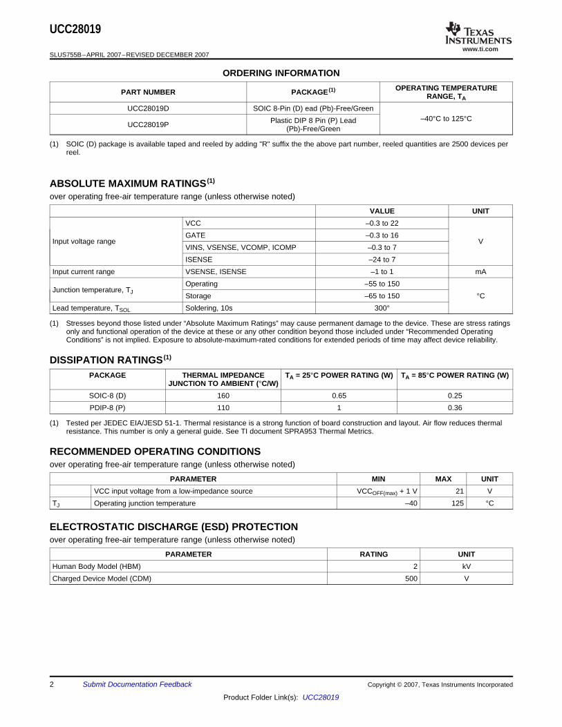
ABSOLUTE MAXIMUM RATINGS (1)
DISSIPATION RATINGS (1)
RECOMMENDED OPERATING CONDITIONS
ELECTROSTATIC DISCHARGE (ESD) PROTECTION
UCC28019
SLUS755B–APRIL 2007–REVISED DECEMBER 2007
ORDERING INFORMATIONOPERATING TEMPERATUREPART NUMBER PACKAGE (1)
RANGE, TA
UCC28019D SOIC 8-Pin (D) ead (Pb)-Free/Green–40°C to 125°CPlastic DIP 8 Pin (P) LeadUCC28019P (Pb)-Free/Green
(1) SOIC (D) package is available taped and reeled by adding "R" suffix the the above part number, reeled quantities are 2500 devices perreel.
over operating free-air temperature range (unless otherwise noted)
VALUE UNITVCC –0.3 to 22GATE –0.3 to 16
Input voltage range VVINS, VSENSE, VCOMP, ICOMP –0.3 to 7ISENSE –24 to 7
Input current range VSENSE, ISENSE –1 to 1 mAOperating –55 to 150
Junction temperature, TJ Storage –65 to 150 °CLead temperature, TSOL Soldering, 10s 300°
(1) Stresses beyond those listed under “Absolute Maximum Ratings” may cause permanent damage to the device. These are stress ratingsonly and functional operation of the device at these or any other condition beyond those included under “Recommended OperatingConditions” is not implied. Exposure to absolute-maximum-rated conditions for extended periods of time may affect device reliability.
PACKAGE THERMAL IMPEDANCE TA = 25°C POWER RATING (W) TA = 85°C POWER RATING (W)JUNCTION TO AMBIENT (°C/W)
SOIC-8 (D) 160 0.65 0.25PDIP-8 (P) 110 1 0.36
(1) Tested per JEDEC EIA/JESD 51-1. Thermal resistance is a strong function of board construction and layout. Air flow reduces thermalresistance. This number is only a general guide. See TI document SPRA953 Thermal Metrics.
over operating free-air temperature range (unless otherwise noted)
PARAMETER MIN MAX UNITVCC input voltage from a low-impedance source VCCOFF(max) + 1 V 21 V
TJ Operating junction temperature –40 125 °C
over operating free-air temperature range (unless otherwise noted)
PARAMETER RATING UNITHuman Body Model (HBM) 2 kVCharged Device Model (CDM) 500 V
2 Submit Documentation Feedback Copyright © 2007, Texas Instruments Incorporated
Product Folder Link(s): UCC28019

www.ti.com
ELECTRICAL CHARACTERISTICS
UCC28019
SLUS755B–APRIL 2007–REVISED DECEMBER 2007
Unless otherwise noted, VCC = 15 VDC, 0.1 µF from VCC to GND, -40°C ≤ TJ = TA ≤ 125°C. All voltages are with respect toGND. Currents are positive into and negative out of the specified terminal.
PARAMETER TEST CONDITIONS MIN TYP MAX UNITVCC Bias SupplyIVCC(start) Pre-start current VCC = VCCON – 0.1 V 25 100 200 µAIVCC(stby) Standby current VSENSE = 0.5 V 1.0 2.1 2.9
mAIVCC(on_load) Operating current VSENSE = 4.5 V, CGATE = 4.7 nF 4 7 10Under Voltage Lockout (UVLO)VCCON Turn on threshold 10.0 10.5 11.0VCCOFF Turn off threshold 9 9.5 10 VUVLO Hysteresis 0.8 1.0 1.2Oscillator
TA = 25°C 61.7 65.0 68.3fSW Switching frequency, kHz
–40°C ≤ TA ≤ 125°C 59 65 71PWM
VCOMP = 0 V, VSENSE = 5 V,DMIN Minimum duty cycle 0%ICOMP = 6.4 VDMAX Maximum duty cycle VSENSE = 4.95 V 94% 97% 99.3%tOFF(min) Minimum off time VSENSE = 3 V, ICOMP = 1 V 100 250 600 nsSystem Protection
ISENSE threshold, soft over currentVSOC -0.66 -0.73 -0.79(SOC) ,ISENSE threshold, peak current LimitVPCL -1.00 -1.08 -1.15 V(PCL) ,VSENSE threshold, open loop ICOMP = 1 V, ISENSE = 0 V,VOLP 0.77 0.82 0.86protection (OLP), VCOMP = 1 VOpen loop protection (OLP) internal VSENSE = 0.5 V 100 250 nApull-down currentVSENSE threshold, outputVUVD 4.63 4.75 4.87under-voltage detection (UVD),VSENSE threshold, outputVOVP ISENSE = -0.2 V 5.12 5.25 5.38over-voltage protection (OVP),
VInput brown-out detection (IBOP)VINSBROWNOUT_th 0.76 0.82 0.88high-to-low thresholdInput brown-out Detection (IBOP)VINSENABLE_th 1.4 1.5 1.6low-to-high threshold
IVINS_0 V VINS bias current VINS = 0 V 0 ±0.1 µAICOMP threshold, external overload 0.6 Vprotection
Copyright © 2007, Texas Instruments Incorporated Submit Documentation Feedback 3
Product Folder Link(s): UCC28019

www.ti.com
UCC28019
SLUS755B–APRIL 2007–REVISED DECEMBER 2007
ELECTRICAL CHARACTERISTICS (continued)Unless otherwise noted, VCC = 15 VDC, 0.1 µF from VCC to GND, -40°C ≤ TJ = TA ≤ 125°C. All voltages are with respect toGND. Currents are positive into and negative out of the specified terminal.
PARAMETER TEST CONDITIONS MIN TYP MAX UNITCurrent Loopgmi Transconductance gain TA = 25°C 0.75 0.95 1.15 mS
Output linear range 50 µAICOMP voltage during OLP VSENSE = 0.5 V 3.7 4.0 4.3 V
Voltage LoopVREF Reference voltage -40°C ≤ TA ≤ 125°C 4.90 5.00 5.10 Vgmv Transconductance gain 31.5 42 52.5 µS
Maximum sink current under normal VSENSE = 6 V, VCOMP = 4 V 21 30 38operationSource current under soft start VSENSE = 4 V, VCOMP = 0 V –21 -30 -38 µA
VSENSE = 4 V, VCOMP = 0 V –100 –170 –250Maximum source current under EDRoperation VSENSE = 4 V, VCOMP = 4 V –60 –100 –140Enhanced dynamic response, VSENSE 4.63 4.75 4.87 Vlow threshold, fallingVSENSE input bias current 1 V ≤ VSENSE ≤ 5 V 100 250 nAVCOMP voltage during OLP VSENSE = 0.5 V, IVCOMP = 0.5 mA 0 0.2 0.4 V
GATE DriverGATE current, peak, sinking (1) CGATE = 4.7 nF 2.0
AGATE current, peak, sourcing (1) CGATE = 4.7 nF –1.5GATE rise time CGATE = 4.7 nF, GATE = 2 V to 8 V 40 60
nsGATE fall time CGATE = 4.7 nF, GATE = 8 V to 2 V 25 40GATE low voltage, no load GATE = 0 A 0 0.05GATE low voltage, sinking GATE = 20 mA 0.3 0.8GATE low voltage, sourcing GATE = -20 mA –0.3 –0.8GATE low voltage, sinking VCC = 5 V, GATE = 5 mA 0.2 0.75 1.2
VGATE low voltage, sinking VCC = 5 V, GATE = 20 mA 0.2 0.9 1.5GATE high voltage VCC = 20 V, CGATE = 4.7 nF 11 12.5 14GATE high voltage VCC = 11 V, CGATE = 4.7 nF 9.5 10.5 11.0
VCC = VCCOFF + 0.2 V,GATE high voltage 8.0 9.0 10.2CGATE = 4.7 nF
(1) Not tested. Characterized by design.
4 Submit Documentation Feedback Copyright © 2007, Texas Instruments Incorporated
Product Folder Link(s): UCC28019

www.ti.com
TYPICAL CHARACTERISTICS
0 5 15
VCC - Bias Supply Voltage - V
0
0.5
1.5
2.5
3.0
4.0
10 20
1.0
2.0
3.5
SUPPLY CURRENT
vs
BIAS SUPPLY VOLTAGE
IVCC
Turn ONIVCC
Turn OFF
VSENSE = VINS = 3V
No Gate Load
I VC
C-
Su
pp
lyC
urr
en
t-
mA
-60 -35 -10 65 115 140
TJ
- Temperature - °C
8.0
9.0
11.0
12.0
15 40 90
10.0
VC
CO
N/V
CC
OF
F-
UV
LO
Th
resh
old
-V
UVLO THRESHOLDS
vs
TEMPERATURE
VCC Turn OFF (VCCOFF
)
VCC Turn ON (VCCON
)
TJ
- Temperature - °C
0
2
4
6
8
10
1
3
5
7
9
I VC
C-
Su
pp
lyC
urr
en
t-
mA
SUPPLY CURRENT
vs
TEMPERATURE
Operating, GATE Load = 4.7 nF
IVCC(on_load)
Standby
IVCC(stby)
-60 -35 -10 65 115 14015 40 90
TJ
- Temperature - °C
0
0.1
0.2
0.3
0.4
0.5
I VC
C(s
tart
)-
Su
pp
lyC
urr
en
t-
mA
SUPPLY CURRENT
vs
TEMPERATURE
Pre-Start
(IVCC(start)
)
VCC = VCCON
- 0.1 V
-60 -35 -10 65 115 14015 40 90
UCC28019
SLUS755B–APRIL 2007–REVISED DECEMBER 2007
Unless otherwise noted, VCC = 15 VDC, 0.1 µF from VCC to GND, TJ = TA = 25°C. All voltages are with respectto GND. Currents are positive into and negative out of the specified terminal.
Figure 1. Figure 2.
Figure 3. Figure 4.
Copyright © 2007, Texas Instruments Incorporated Submit Documentation Feedback 5
Product Folder Link(s): UCC28019

www.ti.com
TJ
- Temperature - °C
55
59
63
67
71
75
f SW
-S
wit
ch
ing
Fre
qu
en
cy
-kH
z
OSCILLATOR FREQUENCY
vs
TEMPERATURE
Switching Frequency
57
61
65
69
73
-60 -35 -10 65 115 14015 40 90 10 16
VCC - Bias Supply Voltage - V
55
59
63
67
71
75
f SW
-S
wit
ch
ing
Fre
qu
en
cy
-kH
z
OSCILLATOR FREQUENCY
vs
BIAS SUPPLY VOLTAGE
57
61
65
69
73
Switching Frequency
20181412
TJ
- Temperature - °C
0
0.4
0.8
1.2
1.6
2.0
gm
i-
Gain
-m
A/V
CURRENT AVERAGING
AMPLIFIER TRANSCONDUCTANCE
vs
TEMPERATURE
Gain
0.2
0.6
1.0
1.4
1.8
-60 -35 -10 65 115 14015 40 90
TJ
- Temperature - °C
30
34
38
42
46
50
gm
v-
Gain
-µ
A/V
VOLTAGE ERROR AMPLIFIER
TRANSCONDUCTANCE
vs
TEMPERATURE
32
36
40
44
48
Gain
-60 -35 -10 65 115 14015 40 90
UCC28019
SLUS755B–APRIL 2007–REVISED DECEMBER 2007
TYPICAL CHARACTERISTICS (continued)
Figure 5. Figure 6.
Figure 7. Figure 8.
6 Submit Documentation Feedback Copyright © 2007, Texas Instruments Incorporated
Product Folder Link(s): UCC28019

www.ti.com
TJ
- Temperature - °C
4.50
5.25
5.50
VO
VP
/V
UV
D-
VS
EN
SE
Th
resh
old
-V
VSENSE THRESHOLD
vs
TEMPERATURE
4.75
5.00
Under-Voltage Protection (VUVD
)
Over-Voltage Protection (VOVP
)
-60 -35 -10 65 115 14015 40 90
TJ
- Temperature - °C
0
0.4
0.8
1.2
1.6
2.0
VO
LP
–V
SE
NS
ET
hre
sh
old
-V
VSENSE THRESHOLD
vs
TEMPERATURE
0.2
0.6
1.0
1.4
1.8
-60 -35 -10 65 115 14015 40 90
Open Loop Protection (VOLP
)
TJ
- Temperature - °C
VS
OC
-IS
EN
SE
Th
resh
old
-V
ISENSE THRESHOLD
vs
TEMPERATURE
Soft Over-Current Protection (SOC)
-60 -35 -10 65 115 14015 40 90
0
-0.2
-0.4
-0.6
-0.8
-1.0
-0.1
-0.3
-0.5
-0.7
-0.9
TJ
- Temperature - °C
0
0.4
0.8
1.2
1.6
2.0
VIN
SE
NA
BL
E_
TH
/V
INS
BR
OU
WN
OU
T_
TH
–V
INS
Th
resh
old
-V
VINS THRESHOLD
vs
TEMPERATURE
0.2
0.6
1.0
1.4
1.8
-60 -35 -10 65 115 14015 40 90
VINS Enable (VINSENABLE_TH
)
Input Brown-Out Protection (VINSBROWNOUT_TH
)
UCC28019
SLUS755B–APRIL 2007–REVISED DECEMBER 2007
TYPICAL CHARACTERISTICS (continued)
Figure 9. Figure 10.
Figure 11. Figure 12.
Copyright © 2007, Texas Instruments Incorporated Submit Documentation Feedback 7
Product Folder Link(s): UCC28019
www.ti.com
TJ
- Temperature - °C
100
200
300
400
500
600
t-
Tim
e-
ns
MINIMUM OFF TIME
vs
TEMPERATURE
tOFF(min)
VSENSE = 3 V
ICOMP = 1 V
105
250
350
450
550
-60 -35 -10 65 115 14015 40 90
TJ
- Temperature - °C
0
10
20
30
40
50
t-
Tim
e-
ns
GATE DRIVE SWITCHING
vs
TEMPERATURE
Fall Time
CGATE
= 4.7 nF
VGATE
= 2 V - 8 V
Rise Time
5
15
25
35
45
-60 -35 -10 65 115 14015 40 90
10 12 16 20
VCC - Bias Supply Voltage - V
0
10
20
30
40
50
18
t-
Tim
e-
ns
GATE DRIVE SWITCHING
vs
BIAS SUPPLY VOLTAGE
Fall Time
CGATE
= 4.7 nF
VGATE
= 2 V - 8 V
Rise Time
5
15
25
35
45
14
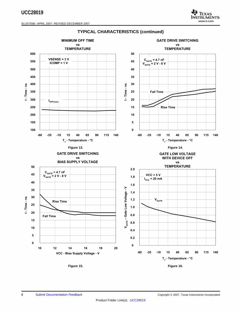
TJ
- Temperature - °C
0
0.4
0.8
1.2
1.6
2.0
VG
AT
E–
Gate
Lo
wV
olt
ag
e-
V
GATE LOW VOLTAGE
WITH DEVICE OFF
vs
TEMPERATURE
0.2
0.6
1.0
1.4
1.8
-60 -35 -10 65 115 14015 40 90
VGATE
VCC = 5 V
IVCC
= 20 mA
UCC28019
SLUS755B–APRIL 2007–REVISED DECEMBER 2007
TYPICAL CHARACTERISTICS (continued)
Figure 13. Figure 14.
Figure 15. Figure 16.
8 Submit Documentation Feedback Copyright © 2007, Texas Instruments Incorporated
Product Folder Link(s): UCC28019
www.ti.com
TJ
- Temperature - °C
4.50
4.75
5.00
5.25
5.50
VR
EF
-R
efe
ren
ce
Vo
lta
ge
-V
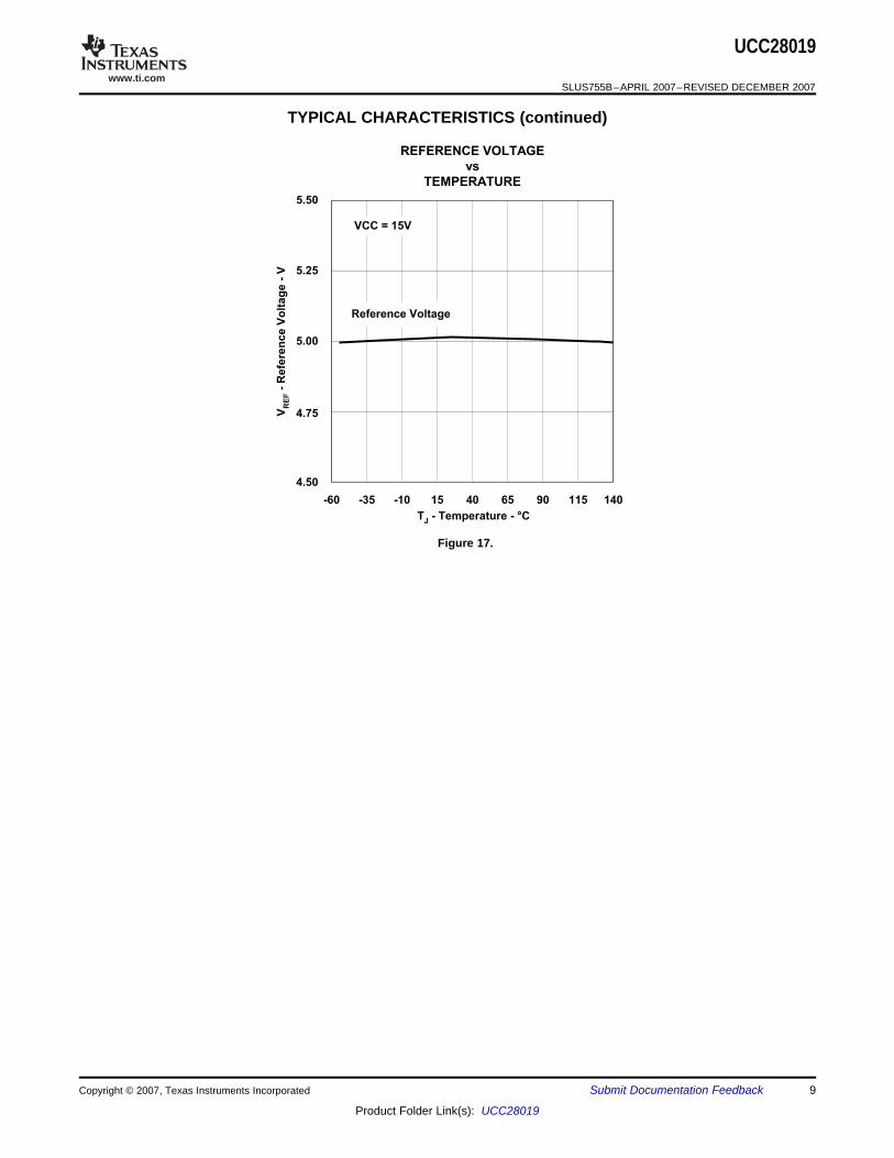
REFERENCE VOLTAGE
vs
TEMPERATURE
Reference Voltage
VCC = 15V
-60 -35 -10 65 115 14015 40 90
UCC28019
SLUS755B–APRIL 2007–REVISED DECEMBER 2007
TYPICAL CHARACTERISTICS (continued)
Figure 17.
Copyright © 2007, Texas Instruments Incorporated Submit Documentation Feedback 9
Product Folder Link(s): UCC28019

www.ti.com
DEVICE INFORMATION
Connection Diagram
GND
ICOMP
ISENSE
GATE
VCC
VSENSE
VCOMPVINS
1
2
3
4
8
7
6
5
Pin Descriptions
UCC28019
SLUS755B–APRIL 2007–REVISED DECEMBER 2007
UCC28019 Top View (SOIC-8, PDIP-8)
Terminal FunctionsTERMINAL
I/O FUNCTIONNAME #
Gate drive: Integrated push-pull gate driver for one or more external power MOSFETs. 2.0-A sink and 1.5-AGATE 8 O source capability. Output voltage is clamped at 12.5 V.GND 1 Ground: Device ground reference.
Current loop compensation: Transconductance current amplifier output. A capacitor connected to GNDICOMP 2 O provides compensation and averaging of the current sense signal in the current control loop. The controller is
disabled if the voltage on ICOMP is less than 0.6 V.Inductor current sense: An input for the voltage across the external current sense resistor, which representsthe instantaneous current through the PFC boost inductor. This voltage is averaged to eliminate the effects of
ISENSE 3 I noise and ripple. Soft Over Current (SOC) limits the average inductor current. Cycle-by-cycle peak currentlimit (PCL) immediately shuts off the GATE drive if the peak-limit voltage is exceeded. Use a 220-Ω resistorbetween this pin and the current sense resistor to limit inrush-surge currents into this pin.Device supply: External bias supply input. Under Voltage Lock Out (UVLO) disables the controller until VCCexceeds a turn-on threshold of 10.5 V. Operation continues until VCC falls below the turn-off (UVLO)VCC 7 threshold of 9.5 V. A ceramic by-pass capacitor of 0.1 µF minimum value should be connected from VCC toGND as close to the device as possible for high frequency filtering of the VCC voltage.Voltage loop compensation: Transconductance voltage error amplifier output. A resistor-capacitor networkconnected from this pin to GND provides compensation. VCOMP is held at GND until VCC, VINS, andVSENSE all exceed their threshold voltages. Once these conditions are satisfied, VCOMP is charged until theVCOMP 5 O VSENSE voltage reaches 95% of its nominal regulation level. When the Enhanced Dynamic Response (EDR)is engaged, additional current is applied to VCOMP to reduce the charge time. EDR additional current isinhibited during soft-start. Soft-start is programmed by the capacitance on this pin.Input ac voltage sense: Input Brown Out Protection (IBOP) detects when the system ac-input voltage isabove a user-defined normal operating level, or below a user-defined “brown-out” level. A filteredresistor-divider network connects from this pin to the rectified-mains node. At startup the controller is disabledVINS 4 I until the VINS voltage exceeds a threshold of 1.5 V, initiating a soft-start. The controller is also disabled ifVINS drops below the brown-out threshold of 0.8 V. Operation will not resume until both VINS and VSENSEvoltages exceed their enable thresholds, initiating another soft-start.Output voltage sense: An external resistor-divider network connected from this pin to the PFC outputvoltage provides feedback sensing for output voltage regulation. A small capacitor from this pin to GND filtershigh-frequency noise. Standby disables the controller and discharges VCOMP when the voltage at VSENSEdrops below the enable threshold of 0.8V. An internal 100nA current source pulls VSENSE to GND forVSENSE 6 I Open-Loop Protection (OLP), including pin disconnection. Output over-voltage protection (OVP) disables theGATE output when VSENSE exceeds 105% of the reference voltage. Enhanced Dynamic Response (EDR)rapidly returns the output voltage to its normal regulation level when a system line or load step causesVSENSE to fall below 95% of the reference voltage.
10 Submit Documentation Feedback Copyright © 2007, Texas Instruments Incorporated
Product Folder Link(s): UCC28019

www.ti.com
+OLP/STANDBY
0.82V
OLP/STANDBY
+
OVERVOLTAGE
5.25VOVP
Input Brown-Out Protection
(IBOP)
+
+
VINENABLE_th
1.5VS Q
QRVIN
BROWNOUT_th0.82V
5V
20k
IBOP
+
VPCL
1.08V
Soft Over Current (SOC)
VSOC
0.73V
Peak Current Limit (PCL)
SOC
40k 40k
+
PCL-1x300ns
Leading Edge
Blanking
UVLO
+
+
VCCON
10.5VSQ
Q RVCC
OFF
9.5VUVLO
RSENSE
COUT
LBST
RISENSEfilter
+–Bridge
Rectifier
CISENSEfilter
LINE
INPUT
DBST
VOUT
CCV2
RCV
CCV1
+gmv
Voltage Error
Amplifier
+gmi
CICOMP
S Q
QR
PWM
Comparator
KPC
(s)
SOC
M2
M1
EMI Filter
ICOMP
VCOMP
CIN
5V
65kHz
Oscillator
RLOAD
CVCC
Auxilary
Supply
Current
Amplifier
3
ISENSE
2
ICOMP
VINS
4
5
VCOMP
6
VSENSE
7
1
VCC
GND
8
GATEGAIN
M1, K
1
EDR
+UNDERVOLTAGE
4.75V
EDR
CVINS
RVINS1
RVINS2
VCC
Gate Driver
UVLO
IBOP
OLP
S Q
QR
OVP
Pre-Drive and
Clamp Circuit
RFB1
RFB2
QBST
10k
RGATE
CVSENSE
+
PWM
RAMP
M2 Min Off Time
+
SSEDR
Fault
Logic
Fault
100µA
4V
FAULT
PCL
Clock
FAULT
4V
UCC28019
SLUS755B–APRIL 2007–REVISED DECEMBER 2007
Figure 18. Block Diagram
Copyright © 2007, Texas Instruments Incorporated Submit Documentation Feedback 11
Product Folder Link(s): UCC28019

www.ti.com
APPLICATION INFORMATION
UCC28019 Operation
UCC28019
SLUS755B–APRIL 2007–REVISED DECEMBER 2007
The UCC28019 is a switch-mode controller used in boost converters for power factor correction operating at afixed frequency in continuous conduction mode. The UCC28019 requires few external components to operate asan active PFC pre-regulator. Its trimmed oscillator provides a nominal fixed switching frequency of 65 kHz,ensuring that both the fundamental and second harmonic components of the conducted-EMI noise spectrum arebelow the EN55022 conducted-band 150-kHz measurement limit.
Its tightly-trimmed internal 5-V reference voltage provides for accurate output voltage regulation over the typicalworld-wide 85 VAC to 265 VAC mains input range from zero to full output load. The usable system load rangesfrom 100 W to 2 kW and may be extended in special situations.
Regulation is accomplished in two loops. The inner current loop shapes the average input current to match thesinusoidal input voltage under continuous inductor current conditions. Under extremely light load conditions,depending on the boost inductor value, the inductor current may go discontinuous but still meet Class-Drequirements of IEC 1000-3-2 despite the higher harmonics. The outer voltage loop regulates the output voltageon VCOMP (dependent upon the line and load conditions) which determines the internal gain parameters formaintaining a low-distortion steady-state input current waveshape.
12 Submit Documentation Feedback Copyright © 2007, Texas Instruments Incorporated
Product Folder Link(s): UCC28019

www.ti.com
Power Supply
VCC
VCCON
10.5V
VCCOFF
9.5VIVCC
IVCC(start)
<200µA
IVCC(stby)
<2.9mA
IVCC(ON)
UVLO Soft-Start UVLORun RunFault/Standby
Controller
State
PWM
StateOFF Ramp Regulated OFF Regulated OFF
Soft-
Start
Ramp
UCC28019
SLUS755B–APRIL 2007–REVISED DECEMBER 2007
The UCC28019 operates from an external bias supply. It is recommended that the device be powered from aregulated auxiliary supply. This device is not intended to be used from a bootstrap bias supply. A bootstrap biassupply is fed from the input high voltage through a resistor with sufficient capacitance on VCC to hold up thevoltage on VCC until current can be supplied from a bias winding on the boost inductor. The minimal hysteresison VCC would require an unreasonable value of hold-up capacitance.
During normal operation, when the output is regulated, current drawn by the device includes the nominal runcurrent plus the current supplied to the gate of the external boost switch. Decoupling of the bias supply must takeswitching current into account in order to keep ripple voltage on VCC to a minimum. A ceramic capacitor with aminimum value of 0.1 µF is recommended from VCC to GND with short, wide traces.
Figure 19. Device Supply States
The device bias operates in several states. During startup, VCC Under-Voltage LockOut (UVLO) sets theminimum operational dc input voltage of the PFC controller. There are two UVLO thresholds. When the UVLOturn-on threshold is exceeded, the controller turns ON. If VCC falls below the UVLO lower turn-off threshold, thecontroller turns OFF. During UVLO, current drawn by the device is minimal. After the device turns on, Soft Start(SS) is initiated and the output is ramped up in a controlled manner to reduce the stress on the externalcomponents and prevents output voltage overshoot. During soft start and after the output is in regulation, thedevice draws its normal run current. If any of several fault conditions is encountered or if the device is put inStandby with an external signal, the device draws a reduced standby current.
Copyright © 2007, Texas Instruments Incorporated Submit Documentation Feedback 13
Product Folder Link(s): UCC28019

www.ti.com
Soft Start
5V
VCOMP
VCOMP
FAULT
gmv
ISS
= -30uA
for VSENSE < 4.75V
during Soft-Start
+
VSENSE
System Protection
Feedback
Voltage
OVP 105% VREF
OLPSoft-Start
(No EDR)OLP
OVP
(No Gate Output)Run
UVD
(EDR on)
Protection
State
100% VREF
OLP/SS 16% VREF
Run
EDR 95% VREF
UCC28019
SLUS755B–APRIL 2007–REVISED DECEMBER 2007
VCOMP, the output of the voltage loop transconductance amplifier, is pulled low during UVLO, IBOP, andOLP(Open-Loop Protection)/STANDBY. After the fault condition is released, soft start controls the rate of rise ofVCOMP in order to obtain a linear control of the increasing duty cycle as a function of time. During soft start aconstant 30 µA of current is sourced into the compensation components causing the voltage on this pin to ramplinearly until the output voltage reaches 85% of its final value. At this point, the sourcing current begins todecrease until the output voltage reaches 95% of its final rated voltage. The soft-start time is controlled by thevoltage error amplifier compensation components selected, and is user-programmable based on desired loopcrossover frequency. Once VOUT exceeds 95% of rate voltage, EDR is no longer inhibited.
Figure 20. Soft Start
System level protection features keep the system in safe operating limits:
Figure 21. Output Protection States
14 Submit Documentation Feedback Copyright © 2007, Texas Instruments Incorporated
Product Folder Link(s): UCC28019
www.ti.com
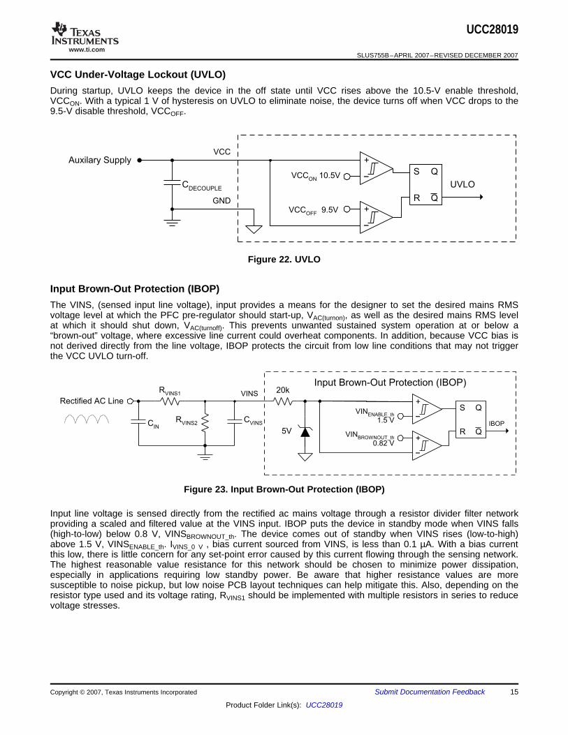
VCC Under-Voltage Lockout (UVLO)
+
+
VCCON
10.5V S Q
QR
CDECOUPLE
VCCAuxilary Supply
GNDVCC
OFF9.5V
UVLO
Input Brown-Out Protection (IBOP)
Input Brown-Out Protection (IBOP)
+
+
VINENABLE_th
1.5 V
S Q
QRVINBROWNOUT_th
0.82 V
CVINS
Rectified AC Line
RVINS1
RVINS2
VINS
5V
20k
IBOPCIN
UCC28019
SLUS755B–APRIL 2007–REVISED DECEMBER 2007
During startup, UVLO keeps the device in the off state until VCC rises above the 10.5-V enable threshold,VCCON. With a typical 1 V of hysteresis on UVLO to eliminate noise, the device turns off when VCC drops to the9.5-V disable threshold, VCCOFF.
Figure 22. UVLO
The VINS, (sensed input line voltage), input provides a means for the designer to set the desired mains RMSvoltage level at which the PFC pre-regulator should start-up, VAC(turnon), as well as the desired mains RMS levelat which it should shut down, VAC(turnoff). This prevents unwanted sustained system operation at or below a“brown-out” voltage, where excessive line current could overheat components. In addition, because VCC bias isnot derived directly from the line voltage, IBOP protects the circuit from low line conditions that may not triggerthe VCC UVLO turn-off.
Figure 23. Input Brown-Out Protection (IBOP)
Input line voltage is sensed directly from the rectified ac mains voltage through a resistor divider filter networkproviding a scaled and filtered value at the VINS input. IBOP puts the device in standby mode when VINS falls(high-to-low) below 0.8 V, VINSBROWNOUT_th. The device comes out of standby when VINS rises (low-to-high)above 1.5 V, VINSENABLE_th. IVINS_0 V , bias current sourced from VINS, is less than 0.1 µA. With a bias currentthis low, there is little concern for any set-point error caused by this current flowing through the sensing network.The highest reasonable value resistance for this network should be chosen to minimize power dissipation,especially in applications requiring low standby power. Be aware that higher resistance values are moresusceptible to noise pickup, but low noise PCB layout techniques can help mitigate this. Also, depending on theresistor type used and its voltage rating, RVINS1 should be implemented with multiple resistors in series to reducevoltage stresses.
Copyright © 2007, Texas Instruments Incorporated Submit Documentation Feedback 15
Product Folder Link(s): UCC28019

www.ti.com
2 1
2
ENABLE _th(max)
VINS VINS
AC( on ) ENABLE _th(max) F _ BRIDGE
VINSR R
V VINS V=
- -
2
1 2
IN _ RMS
VINS
VINS VINS
VP
R R=
+
2
2
1 2
0 9
CVIN _ dschg
VINS
BROWNOUT _th(min)
VINSVINS
IN _ RMS(min)
VINS VINS
tC
VINSR n
R. V ( )
R R
-
=
é ù
ê ú
ê ú
ê ú
ê ú+ë û
l
2
half _ cycles
CVINS _ dschrg
LINE(min)
Nt
f=
UCC28019
SLUS755B–APRIL 2007–REVISED DECEMBER 2007
First, select RVINS1 based on the the highest reasonable resistance value available for typical applications.
Then select RVINS2 based on this value:
Where VF_Bridge is the forward voltage drop across the ac rectifier bridge.
Power dissipated in the resistor network is:
The filter capacitor, CVINS, has two functions. First, to attenuate the voltage ripple to levels between the enableand brown-out thresholds which will prevent the ripple on VINS from falsely triggering IBOP when the converteris operating at low line. Second, CVINS delays the brown-out protection operation for a desired number of linehalf-cycle periods while still having a good response to an actual brown-out event.
The capacitor is chosen so that it will discharge to the VINSBROWNOUT_th level after N number of half line cycles ofdelay to accommodate line dropouts.
Where:
and VIN_RMS(min) is the lowest normal operating RMS input voltage.
16 Submit Documentation Feedback Copyright © 2007, Texas Instruments Incorporated
Product Folder Link(s): UCC28019

www.ti.com
Output Over-Voltage Protection (OVP)
Open Loop Protection/Standby (OLP/Standby)
Output Under-Voltage Detection (UVD) / Enhanced Dynamic Response (EDR)
+OPEN LOOP
PROTECTION/
STANDBY
RFB1
Output Voltage
Standby
OLP/STANDBY
RFB2
+
OVERVOLTAGE
OVP
VSENSE
Optional
+UNDERVOLTAGE UVD4.75V
5.25V
0.82V
UCC28019
SLUS755B–APRIL 2007–REVISED DECEMBER 2007
VOUT(OVP) is the output voltage exceeding 5% of the rated value, causing VSENSE to exceed a 5.25-V threshold(5-V reference voltage + 5%), VOVP. The normal voltage control loop is bypassed and the GATE output isdisabled until VSENSE falls below 5.25 V. For example, VOUT(OVP) is 420 V in a system with a 400-V rated output.
If the output voltage feedback components were to fail and disconnect (open loop) the signal from the VSENSEinput, then it is likely that the voltage error amp would increase the GATE output to maximum duty cycle. Toprevent this, an internal pull-down forces VSENSE low. If the output voltage falls below 16% of its rated voltage,causing VSENSE to fall below 0.8 V, the device is put in Standby, a state where the PWM switching is haltedand the device is still on but draws standby current below 3 mA. This shutdown feature also gives the designerthe option of pulling VSENSE low with an external switch.
During large changes in load, Enhanced Dynamic Response (EDR) acts to speed up the slow response of thelow-bandwidth voltage loop.
Figure 24. Over Voltage Protection, Open Loop Protection/Standby
Copyright © 2007, Texas Instruments Incorporated Submit Documentation Feedback 17
Product Folder Link(s): UCC28019
www.ti.com
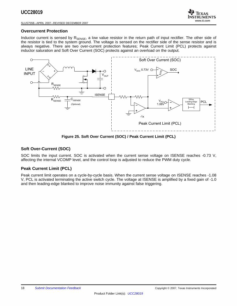
Overcurrent Protection
PCL
+
VPCL
1.08V
ISENSE
Soft Over Current (SOC)
RSENSE
RISENSE
+–
CISENSE
(Optional)
LINE
INPUT VOUT
VSOC
0.73V
Peak Current Limit (PCL)
SOC
+
-1x
300ns
Leading Edge
Blanking
+
Soft Over-Current (SOC)
Peak Current Limit (PCL)
UCC28019
SLUS755B–APRIL 2007–REVISED DECEMBER 2007
Inductor current is sensed by RSENSE, a low value resistor in the return path of input rectifier. The other side ofthe resistor is tied to the system ground. The voltage is sensed on the rectifier side of the sense resistor and isalways negative. There are two over-current protection features; Peak Current Limit (PCL) protects againstinductor saturation and Soft Over Current (SOC) protects against an overload on the output.
Figure 25. Soft Over Current (SOC) / Peak Current Limit (PCL)
SOC limits the input current. SOC is activated when the current sense voltage on ISENSE reaches -0.73 V,affecting the internal VCOMP level, and the control loop is adjusted to reduce the PWM duty cycle.
Peak current limit operates on a cycle-by-cycle basis. When the current sense voltage on ISENSE reaches -1.08V, PCL is activated terminating the active switch cycle. The voltage at ISENSE is amplified by a fixed gain of -1.0and then leading-edge blanked to improve noise immunity against false triggering.
18 Submit Documentation Feedback Copyright © 2007, Texas Instruments Incorporated
Product Folder Link(s): UCC28019

www.ti.com
Current Sense Resistor, RSENSE
1 25
SOC(min)
SENSE
L _ PEAK(max)
VR
. I£
2
RSENSE IN _ RMS (max) SENSEP ( I ) R=
PCLPCL
SENSE
VI
R=
Gate Driver
VCC
VCC
GATEC
OUT
LBST D
BST VOUT
Rectified
AC
GND
RGATE
UVLO
IBOP
OLP
From
PWM
Latch
10kS Q
QR
PCLOVP
Clock Pre-Drive and
Clamp Circuit
QBST
Fault
Logic
UCC28019
SLUS755B–APRIL 2007–REVISED DECEMBER 2007
The current sense resistor, RSENSE, is sized using the minimum threshold value of Soft Over Current (SOC),VSOC(min) = 0.66 V. To avoid triggering this threshold during normal operation, taking into account the gain of theinternal non-linear power limit, resulting in a decreased duty cycle, the resistor is typically sized for an overloadcurrent of 25% more than the peak inductor peak current.
Since RSENSE sees the average input current, worst-case power dissipation occurs at input low line when inputline current is at its maximum. Power dissipated by the sense resistor is:
Peak Current Limit (PCL) protection turns off the output driver when the voltage across the sense resistorreaches the PCL threshold, VPCL. The absolute maximum peak current, IPCL, is given as:
The GATE output is designed with a current-optimized structure to directly drive large values of total MOSFETgate capacitance at high turn-on and turn-off speeds. An internal clamp limits voltage on the MOSFET gate to12.5 V. An external gate drive resistor, RGATE, limits the rise time and dampens ringing caused by parasiticinductances and capacitances of the gate drive circuit thus reducing EMI. The final value of the resistor dependsupon the parasitic elements associated with the layout and other considerations. A 10-kΩ resistor close to thegate of the MOSFET, between the gate and ground, discharges stray gate capacitance and protects againstinadvertent dv/dt-triggered turn-on.
Figure 26. Gate Driver
Copyright © 2007, Texas Instruments Incorporated Submit Documentation Feedback 19
Product Folder Link(s): UCC28019
www.ti.com
Current Loop
ISENSE and ICOMP Functions
Pulse Width Modulator
Control Logic
Voltage Loop
Output Sensing
UCC28019
SLUS755B–APRIL 2007–REVISED DECEMBER 2007
The overall system current loop consists of the current averaging amplifier stage, the pulse width modulator(PWM) stage, the external boost inductor stage, and the external current sensing resistor.
The negative polarity signal from the current sense resistor is buffered and inverted at the ISENSE input. Theinternal positive signal is then averaged by the current amplifier (gmi), whose output is the ICOMP pin. Thevoltage on ICOMP is proportional to the average inductor current. An external capacitor to GND is applied to theICOMP pin for current loop compensation and current ripple filtering. The gain of the averaging amplifier isdetermined by the internal VCOMP voltage. This gain is non-linear to accommodate the world-wide ac-linevoltage range. ICOMP is connected to 4 V internally whenever the device is in a Fault or Standby condition.
The PWM stage compares the ICOMP signal with a periodic ramp to generate a leading-edge-modulated outputsignal which is high whenever the ramp voltage exceeds the ICOMP voltage. The slope of the ramp is defined bya non-linear function of the internal VCOMP voltage.
The PWM output signal always starts low at the beginning of the cycle, triggered by the internal clock. The outputstays low for a minimum off-time, tOFF(min), after which the ramp rises linearly to intersect the ICOMP voltage. Theramp-ICOMP intersection determines tOFF, and hence DOFF. Since DOFF = VIN/VOUT by the boost-topology equation,and since VIN is sinusoidal in wave-shape, and since ICOMP is proportional to the inductor current, it follows thatthe control loop forces the inductor current to follow the input voltage wave-shape to maintain boost regulation.Therefore, the average input current is also sinusoidal in wave-shape.
The output of the PWM comparator stage is conveyed to the GATE drive stage, subject to control by variousprotection functions incorporated into the IC. The GATE output duty-cycle may be as high as 99%, but willalways have a minimum off-time tOFF(min). Normal duty-cycle operation can be interrupted directly by OVP andPCL on a cycle-by-cycle basis. UVLO, IBOP and OLP/Standby also terminate the GATE output pulse, andfurther inhibit output until the SS operation can begin.
The outer control loop of the PFC controller is the voltage loop. This loop consists of the PFC output sensingstage, the voltage error amplifier stage, and the non-linear gain generation.
A resistor-divider network from the PFC output voltage to GND forms the sensing block for the voltage controlloop. The resistor ratio is determined by the desired output voltage and the internal 5-V regulation referencevoltage.
Like the VINS input, the very low bias current at the VSENSE input allows the choice of the highest practicableresistor values for lowest power dissipation and standby current. A small capacitor from VSENSE to GND servesto filter the signal in a high-noise environment. This filter time constant should generally be less than 100 µs.
20 Submit Documentation Feedback Copyright © 2007, Texas Instruments Incorporated
Product Folder Link(s): UCC28019

www.ti.com
Voltage Error Amplifier
Non-linear Gain Generation
UCC28019
SLUS755B–APRIL 2007–REVISED DECEMBER 2007
The transconductance error amplifier (gmv) generates an output current proportional to the difference betweenthe voltage feedback signal at VSENSE and the internal 5-V reference. This output current charges ordischarges the compensation network capacitors on the VCOMP pin to establish the proper VCOMP voltage forthe system operating conditions. Proper selection of the compensation network components leads to a stablePFC pre-regulator over the entire ac-line range and 0-100% load range. The total capacitance also determinesthe rate-of-rise of the VCOMP voltage at soft start, as discussed earlier.
The amplifier output VCOMP is pulled to GND during any Fault or Standby condition to discharge thecompensation capacitors to an initial zero state. Usually, the large capacitor has a series resistor which delayscomplete discharge by their respective time constant (which may be several hundred milliseconds). If VCC biasvoltage is quickly removed after UVLO, the normal discharge transistor on VCOMP loses drive and the largecapacitor could be left with substantial voltage on it, negating the benefit of a subsequent Soft-Start. TheUCC28019 incorporates a parallel discharge path which operates without VCC bias, to further discharge thecompensation network after VCC is removed.
When output voltage perturbations greater than 5% appear at the VSENSE input, the amplifier moves out oflinear operation. On an over-voltage, the OVP function acts directly to shut off the GATE output until VSENSEreturns within 5% of regulation. On an under-voltage, the UVD function invokes EDR which immediatelyincreases the internal VCOMP voltage by 2 V and increases the external VCOMP charging current typically to100 µA to 170 µA. This higher current facilitates faster charging of the compensation capacitors to the newoperating level, improving transient response time.
The voltage at VCOMP is used to set the current amplifier gain and the PWM ramp slope. This voltage isbuffered internally and is then subject to modification by the EDR function and the SOC function, as discussedearlier.
Together the current gain and the PWM slope adjust to the different system operating conditions (set by theac-line voltage and output load level) as VCOMP changes, to provide a low-distortion, high-power-factor inputcurrent wave-shape following that of the input voltage.
Copyright © 2007, Texas Instruments Incorporated Submit Documentation Feedback 21
Product Folder Link(s): UCC28019

www.ti.com
Layout Guidelines
Cut out in
ground plane
Signal
GND
Power
GND
GND
ICOMP
ISENSE
VINS VCOMP
VSENSE
VCC
GATE
UCC28019
SLUS755B–APRIL 2007–REVISED DECEMBER 2007
As with all PWM controllers, the effectiveness of the filter capacitors on the signal pins depends upon theintegrity of the ground return. The pinout of the UCC28019 is ideally suited for separating the high di/dt inducednoise on the power ground from the low current quiet signal ground required for adequate noise immunity. A starpoint ground connection at the GND pin of the device can be achieved with a simple cut out in the ground planeof the printed circuit board. As shown in Figure 27, the capacitors on ISENSE, VINS, VCOMP, and VSENSE(C11, C12, C15, C17, and C16, respectively) must all be returned directly to the quiet portion of the groundplane, indicated by Signal GND, and not the high current return path of the converter, shown as the Power GND.Because the example circuit in Figure 27 uses surface mount components, the ICOMP capacitor, C10, has itsown dedicated return to the GND pin.
Figure 27. Recommended Layout for the UCC28019
22 Submit Documentation Feedback Copyright © 2007, Texas Instruments Incorporated
Product Folder Link(s): UCC28019

www.ti.com
DESIGN EXAMPLE
350-W, Universal Input, 390-VDC Output, PFC Converter
Design Goals
UCC28019
SLUS755B–APRIL 2007–REVISED DECEMBER 2007
This example illustrates the design process and component selection for a continuous conduction mode powerfactor correction boost converter utilizing the UCC28019. The target design is a universal input, 350-W PFCdesigned for an ATX supply application. This design process is directly tied to the UCC28019 Design Calculatorspreadsheet that can be found in the Tools section of the UCC28019 product folder on the Texas Instrumentswebsite.
Table 1. Design Goal ParametersPARAMETER TEST CONDITION MIN TYP MAX UNIT
Input characteristicsInput voltage VIN 85 115 265 VACInput frequency fLINE 47 63 Hz
VAC(on) 75IOUT = 0.9 ABrown out voltage VAC
VAC(off) 65IOUT = 0.9 AOutput characteristics
VOUT85 VAC ≤ VIN ≤ 265 VACOutput voltage 370 390 410 VDC47 Hz ≤ fLINE ≤ 63 Hz0 A ≤ IOUT ≤ 0.9 A85 VAC ≤ VIN ≤ 65VACLine regulation 5%IOUT = 0.440 AVIN = 115 VAC, fLINE = 60 Hz 5%0 A ≤ IOUT ≤ 0.9 A
Load regulationVIN = 230 VAC, fLINE = 50 Hz 5%0 A ≤ IOUT ≤ 0.9 AVRIPPLE(SW)VIN = 115 VAC, fLINE = 60 Hz 3.9IOUT = 0.9 AHigh frequency output voltage
ripple VRIPPLE(SW)VIN = 230 VAC , fLINE = 50 Hz 3.9IOUT = 0.9 A
VppVRIPPLE(f_LINE)VIN = 115 VAC, fLINE = 60 Hz, 19.5IOUT = 0.9 ALine frequency output voltage
ripple VRIPPLE(f_LINE)VIN = 230 VAC, fLINE = 50 Hz 19.5IOUT = 0.9 AIOUT
Output load current 85 VAC ≤ VIN ≤ 265 VAC 0.9 A47 Hz ≤ fLINE ≤ 63 Hz
Output power POUT 350 WOutput over voltage protection VOUT(OVP) 410
VOutput under voltage protection VOUT(UVP) 370
Copyright © 2007, Texas Instruments Incorporated Submit Documentation Feedback 23
Product Folder Link(s): UCC28019

www.ti.com
UCC28019
SLUS755B–APRIL 2007–REVISED DECEMBER 2007
Table 1. Design Goal Parameters (continued)PARAMETER TEST CONDITION MIN TYP MAX UNIT
Control loop characteristicsSwitching frequency fSW, TJ = 25°C 61.7 65 68.3 kHz
f(CO)Control loop bandwidth 10 HzVIN = 162 VDC, IOUT = 0.45 APhase margin VIN = 162 VDC, IOUT = 0.45 A 70 degrees
PFPower factor 0.99VIN = 115 VAC, IOUT = 0.9 ATHDVIN = 115 VAC, fLINE = 60 Hz 4.13% 10%IOUT = 0.9 A
Total harmonic distortionTHDVIN = 230 VAC, fLINE = 50 Hz 6.67% 10%IOUT = 0.9 Aη
Full load efficiency VIN = 115 VAC, fLINE = 60 Hz, 0.92IOUT = 0.9 A
Ambient temperature TAMB 50 °C
24 Submit Documentation Feedback Copyright © 2007, Texas Instruments Incorporated
Product Folder Link(s): UCC28019

www.ti.com
+
+
UCC28019
SLUS755B–APRIL 2007–REVISED DECEMBER 2007
The following procedure refers to the schematic shown in Figure 28.
Figure 28. Design Example Schematic
Copyright © 2007, Texas Instruments Incorporated Submit Documentation Feedback 25
Product Folder Link(s): UCC28019

www.ti.com
Current Calculations
OUT (max)
OUT (max)
OUT
PI
V=
3500 9
390OUT (max)
WI . A
V= @
OUT (max)
IN _ RMS(max)
IN(min)
PI
V PFh
=
3504 52
0 92 85 0 99IN _ RMS(max)
WI . A
. V .= =
´ ´
2IN _ PEAK(max) IN _ RMS(max)I I=
2 4 52 6 39IN _ PEAK(max)I . A . A= ´ =
2 IN _ PEAK(max)
IN _ AVG(max)
II
p
=
2 6 394 07IN _ AVG(max)
. AI . A
p
´
= =
Bridge Rectifier
2BRIDGE F _ BRIDGE IN _ AVG(max)P V I=
2 0 95 4 07 7 73BRIDGEP . V . A . W= ´ ´ =
UCC28019
SLUS755B–APRIL 2007–REVISED DECEMBER 2007
First, determine the maximum average output current, IOUT(max):
The maximum input RMS line current, IIN_RMS(max), is calculated using the parameters from Table 1 and theefficiency and power factor initial assumptions:
Based upon the calculated RMS value, the maximum peak input current, IIN_PEAK(max), and the maximum averageinput current, IIN_AVG(max), assuming the waveform is sinusoidal, can be determined.
Assuming a forward voltage drop, VF_BRIDGE, of 0.95 V across the rectifier diodes, BR1, the power loss in theinput bridge, PBRIDGE, can be calculated:
26 Submit Documentation Feedback Copyright © 2007, Texas Instruments Incorporated
Product Folder Link(s): UCC28019

www.ti.com
Input Capacitor
RIPPLE RIPPLE IN _ PEAK(max)I I I= D
0 2RIPPLEI .D =
0 2 6 39 1 28RIPPLEI . . A . A= ´ =
IN _ RIPPLE(max) RIPPLE _ IN IN _ RECTIFIED(min)V V V= D
0 06RIPPLE _ INV .D =
2IN _ RECTIFIED INV V=
2 85 120 2IN _ RECTIFIED(min)V V . V= ´ =
0 06 120 2 7 21IN _ RIPPLE(max)V . . V . V= ´ =
8
RIPPLE
IN
SW IN _ RIPPLE(max)
IC
f V=
1 280 341
8 65 7 21IN
. AC . F
kHz . Vm= =
´ ´
UCC28019
SLUS755B–APRIL 2007–REVISED DECEMBER 2007
Note that the UCC28019 is a continuous conduction mode controller and as such the inductor ripple currentshould be sized accordingly. Allowing an inductor ripple current, IRIPPLE, of 20% and a high frequency voltageripple factor, VRIPPLE_IN, of 6%, the maximum input capacitor value, CIN, is calculated by first determining the inputripple current, IRIPPLE, and the input voltage ripple, VIN_RIPPLE(max):
The value for the input x-capacitor can now be calculated:
Copyright © 2007, Texas Instruments Incorporated Submit Documentation Feedback 27
Product Folder Link(s): UCC28019

www.ti.com
Boost Inductor
2
RIPPLEL _ PEAK(max) IN _ PEAK(max)
II I= +
1 286 39 7 03
2L _ PEAK(max)
. AI . A . A= + =
1OUTBST (min)
SW ( typ ) RIPPLE
V D( D )L
f I
-
³
390 0 5 1 0 51 17
65 1 28BST (min)
V . ( . )L . mH
kHz . A
´ -³ ³
´
OUT IN _ RECTIFIED(min)
(max)
OUT
V VDUTY
V
-
=
2 85 120IN _ RECTIFIED(min)V V V= ´ =
390 1200 692
390(max)
V VDUTY .
V
-
= =
Boost Diode
1250 5DIODE F _ C OUT (max) SW ( typ ) OUT RRP V I . f V Q= +
1251 5F _ CV . V=
0RRQ nC=
1 5 0 897 0 5 65 390 0 1 35DIODEP . V . A . kHz V nC . W= ´ + ´ ´ ´ =
UCC28019
SLUS755B–APRIL 2007–REVISED DECEMBER 2007
The boost inductor, LBST, is selected after determining the maximum inductor peak current, IL_PEAK(max):
The minimum value of the boost inductor is calculated based upon a worst case duty cycle of 0.5:
The actual value of the boost inductor that will be used is 1.25 mH.
The maximum duty cycle, DUTY(max), can be calculated and will occur at the minimum input voltage:
The diode losses are estimated based upon the forward voltage drop, VF, at 125°C and the reverse recoverycharge, QRR, of the diode. Using a silicone carbide diode, although more expensive, will essentially eliminate thereverse recovery losses:
28 Submit Documentation Feedback Copyright © 2007, Texas Instruments Incorporated
Product Folder Link(s): UCC28019
www.ti.com
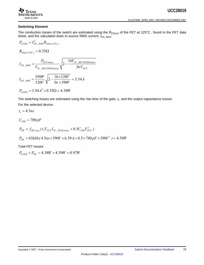
Switching Element
2
125COND DS _ RMS DSon( C )P I R=
1250 35DSon( C )R .= W
162
3
OUT (max) IN _ RECTIFIED(min)
DS _ RMS
IN _ RECTIFIED(min) OUT
P VI
V Vp= -
350 16 1202 3 54
120 3 390DS _ RMS
W VI . A
V Vp
´= - =
´
23 54 0 35 4 38CONDP . A . . W= ´ W =
4 5rt . ns=
780OSSC pF=
20 5SW SW ( typ ) r OUT IN _ PEAK(max) OSS OUTP f ( t V I . C V )= +
265 4 5 390 6 39 0 5 780 390 4 59SWP kHz( . ns V . A . pF V ) . W= ´ ´ + ´ ´ =
4 38 4 59 8 97COND SWP P . W . W . W+ = + =
UCC28019
SLUS755B–APRIL 2007–REVISED DECEMBER 2007
The conduction losses of the switch are estimated using the RDS(on) of the FET at 125°C , found in the FET datasheet, and the calculated drain to source RMS current, IDS_RMS:
The switching losses are estimated using the rise time of the gate, tr, and the output capacitance losses.
For the selected device:
Total FET losses:
Copyright © 2007, Texas Instruments Incorporated Submit Documentation Feedback 29
Product Folder Link(s): UCC28019

www.ti.com
Sense Resistor
1 25
SOCSENSE
L _ PEAK(max)
VR
I .=
´
0 660 075
7 03 1 25SENSE
. VR .
. A .= = W
´
0 067SENSER .= W
SENSERMSINRsense RIP 2
(max)_=
24 52 0 067 1 36RsenseP ( . A ) . . W= ´ W =
PCLPCL
SENSE
VI
R=
1 1517 16
0 067PCL
. VI . A
.= =
W
UCC28019
SLUS755B–APRIL 2007–REVISED DECEMBER 2007
To accommodate the gain of the internal non-linear power limit, RSENSE, is sized such that it will trigger the softover-current at 25% higher than the maximum peak inductor current using the minimum SOC threshold, VSOC, ofISENSE.
Using a parallel combination of available standard value resistors, the sense resistor is chosen.
The power dissipated across the sense resistor, PRsense, must be calculated:
The peak current limit, PCL, protection feature will be triggered when current through the sense resistor results inthe voltage across RSENSE to be equal to the VPCL threshold. For a worst case analysis, the maximum VPCLthreshold is used:
To protect the device from inrush current, a standard 220-Ω resistor, RISENSE, is placed in series with the ISENSEpin. A 1000-pF capacitor is placed close to the device to improve noise immunity on the ISENSE pin.
30 Submit Documentation Feedback Copyright © 2007, Texas Instruments Incorporated
Product Folder Link(s): UCC28019

www.ti.com
Output Capacitor
2 2
2 OUT HOLDUPOUT (min)
OUT OUT _ HOLDUP(min)
P tC
V V³
-
2 2
2 350 21 28240
390 300OUT (min)
W . msC F
V Vm
´ ´³ ³
-
0 05OUT _ RIPPLE( pp ) OUTV . V<
0 05 390 19 5OUT _ RIPPLE( pp ) PPV . V . V< ´ <
2
OUTOUT _ RIPPLE( pp )
LINE(min) OUT
IV
( f )Cp=
0 911 26
2 47 270OUT _ RIPPLE( pp )
. AV . V
( Hz ) Fp m= =
´ ´
2
2
OUT (max)
Cout _ fline
II =
2
0 90 635
2Cout _ fline
. AI . A= =
161 5
3
OUTCout _ HF OUT (max)
IN _ RECTIFIED(min)
VI I .
Vp= -
16 3900 9 1 5 1 8
3 120Cout _ HF
VI . A . . A
Vp
´= - =
´
2 2
2Cout _ RMS( total ) Cout _ fline Cout _ HFI I I= +
2 20 635 1 8 1 9Cout _ RMS( total )I . A . A . A= + =
UCC28019
SLUS755B–APRIL 2007–REVISED DECEMBER 2007
The output capacitor, COUT, is sized to meet holdup requirements of the converter. Assuming the downstreamconverters require the output of the PFC stage to never fall below 300 V, VOUT_HOLDUP(min), during one line cycle,tHOLDUP = 1/fLINE(min), the minimum calculated value for the capacitor is:
It is advisable to de-rate this capacitor value by 20%; the actual capacitor used is 270 µF.
Setting the maximum peak-to-peak output ripple voltage to be less than 5% of the output voltage will ensure thatthe ripple voltage will not trigger the output over-voltage or output under-voltage protection features of thecontroller. The maximum peak-to-peak ripple voltage, occurring at twice the line frequency, and the ripple currentof the output capacitor are calculated:
The required ripple current rating at twice the line frequency is equal to:
There will also be a high frequency ripple current through the output capacitor:
The total ripple current in the output capacitor is the combination of both and the output capacitor must beselected accordingly:
Copyright © 2007, Texas Instruments Incorporated Submit Documentation Feedback 31
Product Folder Link(s): UCC28019
www.ti.com
Output Voltage Set Point
1
2
REF FBFB
OUT REF
V RR
V V=
-
2
5 113 04
390 5FB
V MR . k
V V
´ W= = W
-
1 2
2
FB FBOUT ( OVP ) OVP
FB
R RV VSENSE
R
æ ö+
=ç ÷
è ø
1 135 25 410 7
13OUT ( OVP )
M kV . V . V
k
W + Wæ ö= ´ =ç ÷
Wè ø
1 2
2
FB FBOUT ( UVD ) UVD
FB
R RV VSENSE
R
æ ö+
=ç ÷
è ø
1 134 75 371 6
13OUT ( UVD )
M kV . V . V
k
W + Wæ ö= ´ =ç ÷
Wè ø
UCC28019
SLUS755B–APRIL 2007–REVISED DECEMBER 2007
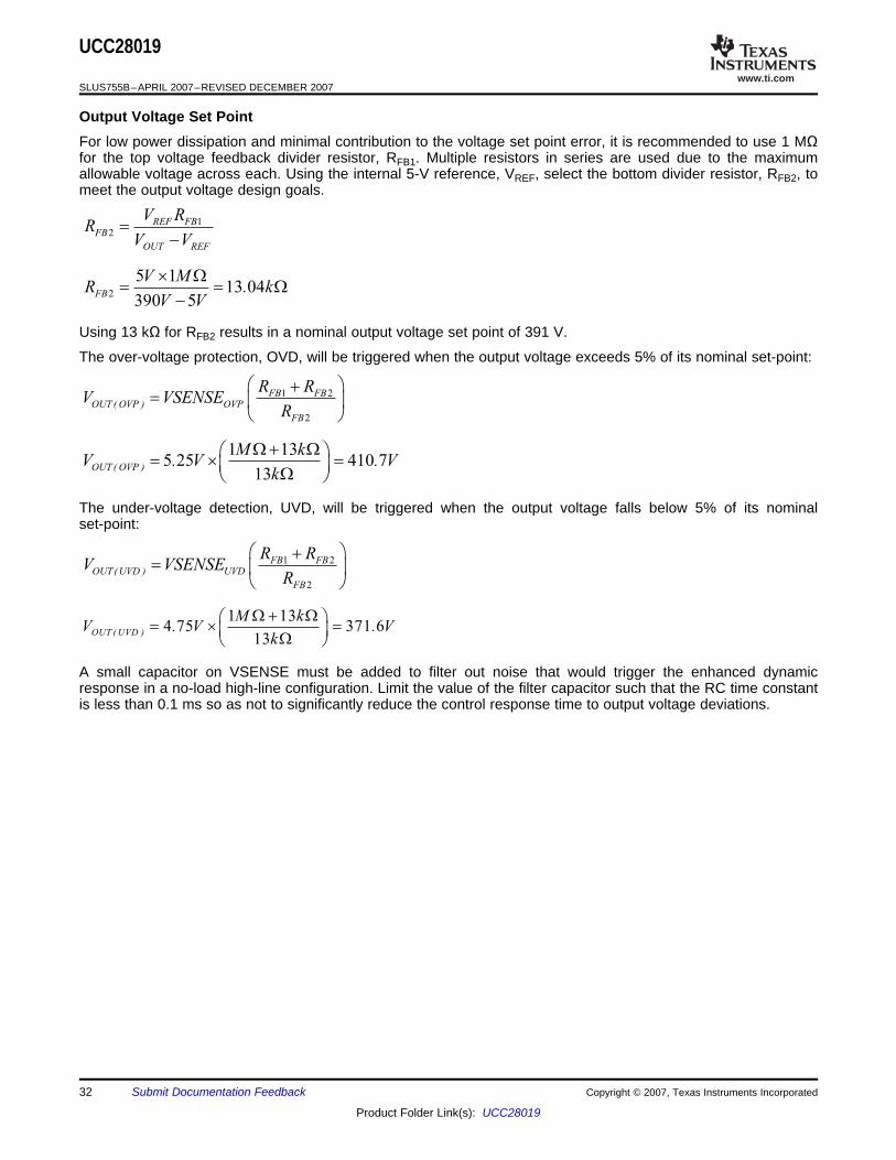
For low power dissipation and minimal contribution to the voltage set point error, it is recommended to use 1 MΩfor the top voltage feedback divider resistor, RFB1. Multiple resistors in series are used due to the maximumallowable voltage across each. Using the internal 5-V reference, VREF, select the bottom divider resistor, RFB2, tomeet the output voltage design goals.
Using 13 kΩ for RFB2 results in a nominal output voltage set point of 391 V.
The over-voltage protection, OVD, will be triggered when the output voltage exceeds 5% of its nominal set-point:
The under-voltage detection, UVD, will be triggered when the output voltage falls below 5% of its nominalset-point:
A small capacitor on VSENSE must be added to filter out noise that would trigger the enhanced dynamicresponse in a no-load high-line configuration. Limit the value of the filter capacitor such that the RC time constantis less than 0.1 ms so as not to significantly reduce the control response time to output voltage deviations.
32 Submit Documentation Feedback Copyright © 2007, Texas Instruments Incorporated
Product Folder Link(s): UCC28019

www.ti.com
Loop Compensation
2
1
1 2 2 2
OUT (max) OUT SENSE
IN _ RMS FQ
I V R KM M
V Kh=
1
FQ
SW ( typ )
Kf
=
115 385
65FQK . s
kHzm= =
17K =
2
1 2 2 2
0 9 390 0 067 70 372
0 92 115 15 385
. A V . VM M .
. V . s sm m
´ ´ W´= =
´ ´
VCOMP - V
0
0.4
0.8
1.2
1.6
2.0
M1M
2
M1M
2
vs
VCOMP
0.2
0.6
1.0
1.4
1.8
0 1 2 5 73 4 6
UCC28019
SLUS755B–APRIL 2007–REVISED DECEMBER 2007
The selection of compensation components, for both the current loop and the voltage loop, is made easier byusing the UCC28019 Design Calculator spreadsheet that can be found in the Tools section of the UCC28019product folder on the Texas Instruments website. The current loop is compensated first by determining theproduct of the internal loop variables, M1M2, using the internal controller constants K1 and KFQ:
The VCOMP operating point is found on Figure 29. The Design Calculator spreadsheet enables the user toiteratively select the appropriate VCOMP value.
Figure 29. M1M2 vs. VCOMP
For the given M1M2 of 0.372 V/µs, the VCOMP, approximately equal to 4, as shown in Figure 29.
Copyright © 2007, Texas Instruments Incorporated Submit Documentation Feedback 33
Product Folder Link(s): UCC28019

www.ti.com
1
0 2
0 064
if : VCOMP
then : M .
< <
=
1
2 3
0 139 0 214
if : VCOMP
then : M . VCOMP .
£ <
= ´ -
1
3 5 5
0 279 0 632
if : VCOMP .
then : M . VCOMP .
£ <
= ´ -
1
5 5 7
0 903
if : . VCOMP
then : M .
£ <
=
1
4
0 279 4 0 632 0 484
VCOMP
M . . .
=
= ´ - =
2
0 1 5
0
if : VCOMP .
Vthen : M
sm
< <
=
2
2
1 5 5 6
0 1223 1 5
if : . VCOMP .
Vthen : M . (VCOMP . )
sm
£ <
= ´ -
2
5 6 7
2 056
if : . VCOMP
Vthen : M .
sm
£ <
=
2
2
4
0 1223 4 1 5 0 764
VCOMP
V VM . ( . ) .
s sm m
=
= ´ - =
UCC28019
SLUS755B–APRIL 2007–REVISED DECEMBER 2007
The individual loop factors, M1 which is the current loop gain factor, and M2 which is the voltage loop PWM rampslope, are calculated using the following conditions:
The M1 current loop gain factor:
The M2 PWM ramp slope:
34 Submit Documentation Feedback Copyright © 2007, Texas Instruments Incorporated
Product Folder Link(s): UCC28019

www.ti.com
1 20 484 0 764 0 37
V VM M . . .
s sm m´ = ´ =
1 20 37 0 372
V V. M M .
s sm m@ =
2
3
0 3
0 0510 0 1543 0 1167
if : VCOMP
then : M . VCOMP . VCOMP .
< <
= ´ - ´ -
2
3
3 7
0 1026 0 3596 0 3085
if : VCOMP
then : M . VCOMP . VCOMP .
£ <
= ´ - ´ +
2
3
4
0 1026 4 0 3596 4 0 3085 0 512
VCOMP
M . . . .
=
= ´ - ´ + =
1
12
ICOMP
IAVG
gmiMC
K fp=
0 95 0 4841100
7 2 9 5ICOMP
. mS .C pF
. kHzp
´= =
´ ´ ´
UCC28019
SLUS755B–APRIL 2007–REVISED DECEMBER 2007
Verify that the product of the individual gain factors is approximately equal to the M1M2 factor determined above,if not, reselect VCOMP and recalculate M1M2.
The non-linear gain variable, M3, can now be calculated:
The frequency of the current averaging pole, fIAVG, is chosen to be at 9.5 kHz. The required capacitor on ICOMP,CICOMP, for this is determined using the transconductance gain, gmi, of the internal current amplifier:
Copyright © 2007, Texas Instruments Incorporated Submit Documentation Feedback 35
Product Folder Link(s): UCC28019

www.ti.com
1
2
11 2
1
1SENSE OUTCL
ICOMPFQ BST
K R VG ( f )
s( f ) K CK M M Ls( f )
gmiM
= ´
+
( )20CLdB CLG ( f ) log G ( f )=
1*104
qG
CL(f
)f - Hz
-100
-60
-20
20
60
100
GC
Ld
B(f
)
CURRENT AVERAGING CIRCUIT
-80
-40
0
40
80
10 100 1*103 1*1061*105
-180
-160
-140
-120
-100
-80
Gain
Phase
UCC28019
SLUS755B–APRIL 2007–REVISED DECEMBER 2007
The transfer function of the current loop can be plotted:
Figure 30. Bode Plot of the Current Averaging Circuit.
36 Submit Documentation Feedback Copyright © 2007, Texas Instruments Incorporated
Product Folder Link(s): UCC28019

www.ti.com
UCC28019
SLUS755B–APRIL 2007–REVISED DECEMBER 2007
The open loop of the voltage transfer function, GVL(f) contains the product of the voltage feedback gain, GFB, andthe gain from the pulse width modulator to the power stage, GPWM_PS, which includes the pulse width modulatorto power stage pole, fPWM_PS. The plotted result is shown in Figure 31.
Copyright © 2007, Texas Instruments Incorporated Submit Documentation Feedback 37
Product Folder Link(s): UCC28019

www.ti.com
2
1 2
FBFB
FB FB
RG
R R=
+
130 013
1 13FB
kG .
M k
W
= =
W + W
3
1
2
1 2
1
2
PWM _ PS
SENSE OUT OUT
FQ IN( typ )
fK R V C
K M M Vp
=
3
2
11 589
7 0 067 390 2702
15 385 0 484 0 764 115
PWM _ PSf . Hz. V F
V. s . . V
s
mp
mm
= =´ W´ ´
´ ´ ´
3
1 21
12
OUT
PWM _ PS
PWM _ PS
M V
M M sG ( f )
s( f )
f
m
p
´=
+
VL FB PWM _ PSG ( f ) G G ( f )=
( )20VLdB VLG ( f ) log G ( f )=
1*104
qG
VL(f
)
f - Hz
-60
20
GV
Ld
B(f
)
OPEN LOOP VOLTAGE TRANSFER
FUNCTION
-40
-20
0
10 100 1*103
-100
-80
-60
-40
-20
0
10.10.01
Gain
Phase
UCC28019
SLUS755B–APRIL 2007–REVISED DECEMBER 2007
Figure 31. Bode Plot of the Open Loop Voltage Transfer Function
38 Submit Documentation Feedback Copyright © 2007, Texas Instruments Incorporated
Product Folder Link(s): UCC28019

www.ti.com
1
2ZERO
VCOMP VCOMP
fR Cp
=
1
2
POLEVCOMP VCOMP VCOMP _ P
VCOMP VCOMP _ P
fR C C
C Cp
=
+
( )
1
1
VCOMP VCOMPEA
VCOMP VCOMP VCOMP _ P
VCOMP VCOMP _ P
VCOMP VCOMP _ P
s( f )R CG ( f ) gmv
R C CC C s( f ) s( f )
C C
é ù
ê ú
ê ú+
=ê ú
é ùæ öê ú
+ +ê úç ÷ê úç ÷
+ê úè øë ûë û
10Vf Hz=
2010 2G ( f )VLdB
V
PWM _ PS
VCOMP
V
fgmv
fC
fp
=
´
0 709
20
1042
1 5893 88
10 2 10. dBVCOMP
HzS
. HzC . FHz
m
m
p
´
= =
´ ´ ´
1
2VCOMP
ZERO VCOMP
Rf Cp
=
130 36
2 1 589 3 3VCOMPR . k
. Hz . Fp m= = W
´ ´ ´
2 1
VCOMPVCOMP _ P
POLE VCOMP VCOMP
CC
f R Cp=
-
3 30 258
2 20 33 3 3 1VCOMP _ P
. FC . F
Hz k . F
mm
p m= =
´ ´ ´ W´ -
UCC28019
SLUS755B–APRIL 2007–REVISED DECEMBER 2007
The voltage error amplifier is compensated with a zero, fZERO, at the fPWM_PS pole and a pole, fPOLE, placed at 20Hz to reject high frequency noise and roll off the gain amplitude. The overall voltage loop crossover, fV, is desiredto be at 10 Hz. The compensation components of the voltage error amplifier are selected accordingly.
From Figure 31, and the Design Calculator spreadsheet, the open loop gain of the voltage transfer function at 10Hz is approximately 0.709 dB. Estimating that the parallel capacitor, CVCOMP_P, is much smaller than the seriescapacitor, CVCOMP, the unity gain will be at fV, and the zero will be at fPWM_PS, the series compensation capacitoris determined:
A 3.3-µF capacitor is used for CVCOMP.
A 33-kΩ resistor is used for RVCOMP.
A 0.22-µF capacitor is used for CVCOMP_P.
Copyright © 2007, Texas Instruments Incorporated Submit Documentation Feedback 39
Product Folder Link(s): UCC28019

www.ti.com
VL _total FB PWM _ PS EAG ( f ) G ( f )G ( f )G ( f )=
( )20VL _totaldB VL _totalG ( f ) log G ( f )=
1*104
f - Hz
-150
100
GV
L_
tota
ldB(f
)
CLOSED LOOP VOLTAGE TRANSFER
FUNCTION
-50
0
50
10 100 1*103
0
20
40
60
80
100
10.10.01
-100
qG
VL
_to
tal(f)
Gain
Phase
UCC28019
SLUS755B–APRIL 2007–REVISED DECEMBER 2007
The total closed loop transfer function, GVL_total, contains the combined stages and is plotted in Figure 32.
Figure 32. Closed Loop Voltage Bode Plot
40 Submit Documentation Feedback Copyright © 2007, Texas Instruments Incorporated
Product Folder Link(s): UCC28019

www.ti.com
Brown Out Protection
0150VINS VINS _ VI I= ´
150 0 1 15VINSI . A Am m= ´ =
75AC( on )V V=
65AC ( off )V V=
1
2 AC( on ) F _ BRIDGE ENABLE _th(max)
VINS
VINS
V V VINSR
I
´ - -=
1
2 75 0 95 1 66 9
15VINS
V . V . VR . M
Am
´ - -= = W
1
2
2
ENABLE _th(max) VINS
VINS
AC( on ) ENABLE _th(max) F _ BRIDGE
VINS RR
V VINS V
´=
´ - -
2
1 6 6 5100
2 75 1 6 0 95VINS
. V . MR k
V . V . V
´ W= = W
´ - -
UCC28019
SLUS755B–APRIL 2007–REVISED DECEMBER 2007
Select the top divider resistor into the VINS pin so as not to contribute excessive power loss. The extremely lowbias current into VINS means the value of RVINS1 could be hundreds of megaohms. For practical purposes, avalue less than 10 MΩ is usually chosen. Assuming approximately 150 times the input bias current through theresistor dividers will result in an RVINS1 that is less than 10 MΩ , so as to not contribute excessive noise, and stillmaintain minimal power loss. The brown out protection will turn off the gate drive when the input falls below theuser programmable minimum voltage, VAC(off), and turn on when the input rises above VAC(on).
A 6.5-M resistance is chosen.
Copyright © 2007, Texas Instruments Incorporated Submit Documentation Feedback 41
Product Folder Link(s): UCC28019

www.ti.com
2
HALF _ CYCLES
CVINS _ dischrg
LINE(min)
Nt
f=
´
2 525 6
2 47CVINS _ dischrg
.t . ms
Hz= =
´
2
2
1 2
0 9
CVINS _ dischrg
VINS
BROWNOUT _th(min)
VINS
VINSIN _ RMS(min)
VINS VINS
tC
VINSR ln
R. V
R R
-=
é ù
ê ú
ê ú´ê úæ ö
´ ´ê úç ÷+ê úè øë û
25 60 63
0 76100
1000 9 85
6 5 100
VINS
. msC . F
. Vk ln
k. V
. M k
m-
= =é ù
ê ú
ê úW´Wæ öê ú
´ ´ç ÷ê úW + Wè øë û
UCC28019
SLUS755B–APRIL 2007–REVISED DECEMBER 2007
The capacitor on VINS, CVINS, is selected so that it's discharge time is greater than the output capacitor hold uptime. COUT was chosen to meet one-cycle hold-up time so CVINS will be chosen to meet 2.5 half-line cycles.
42 Submit Documentation Feedback Copyright © 2007, Texas Instruments Incorporated
Product Folder Link(s): UCC28019

www.ti.com
REFERENCES
RELATED PRODUCTS
UCC28019
SLUS755B–APRIL 2007–REVISED DECEMBER 2007
These references, additional design tools, and links to additional references, including design software andmodels may be found on the web at http://www.power.ti.com under Technical Documents.
Evaluation Module, 350-W Universal Input, 390-VDC Output PFC Converter, Texas Instruments Literature No.SLUA272
Design Spreadsheet, UCC28019 Design Calculator, Texas Instruments
The following parts have characteristics similar to the UCC28019 and may be of interest.
Related ProductsDEVICE DESCRIPTION
UCC3817/18 Full-Feature PFC ControllerUC2853A 8-Pin CCM PFC Controller
Copyright © 2007, Texas Instruments Incorporated Submit Documentation Feedback 43
Product Folder Link(s): UCC28019

TAPE AND REEL INFORMATION
*All dimensions are nominal
Device PackageType
PackageDrawing
Pins SPQ ReelDiameter
(mm)
ReelWidth
W1 (mm)
A0 (mm) B0 (mm) K0 (mm) P1(mm)
W(mm)
Pin1Quadrant
UCC28019DR SOIC D 8 2500 330.0 12.4 6.4 5.2 2.1 8.0 12.0 Q1
PACKAGE MATERIALS INFORMATION
www.ti.com 19-Mar-2008
Pack Materials-Page 1

*All dimensions are nominal
Device Package Type Package Drawing Pins SPQ Length (mm) Width (mm) Height (mm)
UCC28019DR SOIC D 8 2500 340.5 338.1 20.6
PACKAGE MATERIALS INFORMATION
www.ti.com 19-Mar-2008
Pack Materials-Page 2


IMPORTANT NOTICE
Texas Instruments Incorporated and its subsidiaries (TI) reserve the right to make corrections, enhancements, improvements and otherchanges to its semiconductor products and services per JESD46, latest issue, and to discontinue any product or service per JESD48, latestissue. Buyers should obtain the latest relevant information before placing orders and should verify that such information is current andcomplete. All semiconductor products (also referred to herein as “components”) are sold subject to TI’s terms and conditions of salesupplied at the time of order acknowledgment.
TI warrants performance of its components to the specifications applicable at the time of sale, in accordance with the warranty in TI’s termsand conditions of sale of semiconductor products. Testing and other quality control techniques are used to the extent TI deems necessaryto support this warranty. Except where mandated by applicable law, testing of all parameters of each component is not necessarilyperformed.
TI assumes no liability for applications assistance or the design of Buyers’ products. Buyers are responsible for their products andapplications using TI components. To minimize the risks associated with Buyers’ products and applications, Buyers should provideadequate design and operating safeguards.
TI does not warrant or represent that any license, either express or implied, is granted under any patent right, copyright, mask work right, orother intellectual property right relating to any combination, machine, or process in which TI components or services are used. Informationpublished by TI regarding third-party products or services does not constitute a license to use such products or services or a warranty orendorsement thereof. Use of such information may require a license from a third party under the patents or other intellectual property of thethird party, or a license from TI under the patents or other intellectual property of TI.
Reproduction of significant portions of TI information in TI data books or data sheets is permissible only if reproduction is without alterationand is accompanied by all associated warranties, conditions, limitations, and notices. TI is not responsible or liable for such altereddocumentation. Information of third parties may be subject to additional restrictions.
Resale of TI components or services with statements different from or beyond the parameters stated by TI for that component or servicevoids all express and any implied warranties for the associated TI component or service and is an unfair and deceptive business practice.TI is not responsible or liable for any such statements.
Buyer acknowledges and agrees that it is solely responsible for compliance with all legal, regulatory and safety-related requirementsconcerning its products, and any use of TI components in its applications, notwithstanding any applications-related information or supportthat may be provided by TI. Buyer represents and agrees that it has all the necessary expertise to create and implement safeguards whichanticipate dangerous consequences of failures, monitor failures and their consequences, lessen the likelihood of failures that might causeharm and take appropriate remedial actions. Buyer will fully indemnify TI and its representatives against any damages arising out of the useof any TI components in safety-critical applications.
In some cases, TI components may be promoted specifically to facilitate safety-related applications. With such components, TI’s goal is tohelp enable customers to design and create their own end-product solutions that meet applicable functional safety standards andrequirements. Nonetheless, such components are subject to these terms.
No TI components are authorized for use in FDA Class III (or similar life-critical medical equipment) unless authorized officers of the partieshave executed a special agreement specifically governing such use.
Only those TI components which TI has specifically designated as military grade or “enhanced plastic” are designed and intended for use inmilitary/aerospace applications or environments. Buyer acknowledges and agrees that any military or aerospace use of TI componentswhich have not been so designated is solely at the Buyer's risk, and that Buyer is solely responsible for compliance with all legal andregulatory requirements in connection with such use.
TI has specifically designated certain components which meet ISO/TS16949 requirements, mainly for automotive use. Components whichhave not been so designated are neither designed nor intended for automotive use; and TI will not be responsible for any failure of suchcomponents to meet such requirements.
Products Applications
Audio www.ti.com/audio Automotive and Transportation www.ti.com/automotive
Amplifiers amplifier.ti.com Communications and Telecom www.ti.com/communications
Data Converters dataconverter.ti.com Computers and Peripherals www.ti.com/computers
DLP® Products www.dlp.com Consumer Electronics www.ti.com/consumer-apps
DSP dsp.ti.com Energy and Lighting www.ti.com/energy
Clocks and Timers www.ti.com/clocks Industrial www.ti.com/industrial
Interface interface.ti.com Medical www.ti.com/medical
Logic logic.ti.com Security www.ti.com/security
Power Mgmt power.ti.com Space, Avionics and Defense www.ti.com/space-avionics-defense
Microcontrollers microcontroller.ti.com Video and Imaging www.ti.com/video
RFID www.ti-rfid.com
OMAP Applications Processors www.ti.com/omap TI E2E Community e2e.ti.com
Wireless Connectivity www.ti.com/wirelessconnectivity
Mailing Address: Texas Instruments, Post Office Box 655303, Dallas, Texas 75265Copyright © 2012, Texas Instruments Incorporated