Embed Size (px)
Citation preview
1
2
3
6
5
4
VDD
IN-
IN+
VREF
OUTH
OUTL
UCC27611
R1
R2
Q1
IN+
D1
C1
+
VOUT
VSOURCE
L1
C3
VREF4.5 V to 18 V
Non-Inverting Input Inverting Input
C2
VDD
1
2
3
6
5
4
VDD
IN-
IN+
VREF
OUTH
OUTL
UCC27611
R1
R2
Q1
VREF
D1
C1
+
VOUT
VSOURCE
L1
C3
VREF4.5 V to 18 V
C2
VDD
IN-
7
GND
7
GND
Product
Folder
Order
Now
Technical
Documents
Tools &
Software
Support &Community
An IMPORTANT NOTICE at the end of this data sheet addresses availability, warranty, changes, use in safety-critical applications,intellectual property matters and other important disclaimers. PRODUCTION DATA.
UCC27611SLUSBA5F –DECEMBER 2012–REVISED MARCH 2018
UCC27611 5-V, 4-A to 6-A Low Side GaN Driver
1
1 Features1• Enhancement Mode Gallium Nitride FETs
(eGANFETs)• 4-V to 18-V Single Supply Range VDD Range• Drive Voltage VREF Regulated to 5 V• 4-A Peak Source and 6-A Peak Sink Drive
Current• 1-Ω and 0.35-Ω Pullup and Pulldown Resistance
(Maximize High Slew-Rate dV and dt Immunity)• Split Output Configuration (Allows Turnon and
Turnoff Optimization for Individual FETs)• Fast Propagation Delays (14-ns Typical)• Fast Rise and Fall Times (9-ns and 5-ns Typical)• TTL and CMOS Compatible Inputs (Independent
of Supply Voltage Allow Easy Interface-to-Digitaland Analog Controllers)
• Dual-Input Design Offering Drive Flexibility (BothInverting and Noninverting Configurations)
• Output Held Low When Inputs Are Floating• VDD Under Voltage Lockout (UVLO)• Optimized Pinout Compatible With eGANFET
Footprint for Easy Layout• 2.00 mm × 2.00 mm SON-6 Package With
Exposed Thermal and Ground Pad, (MinimizedParasitic Inductances to Reduce Gate Ringing)
• Operating Temperature Range of –40°C to 140°C
2 Applications• Switch-Mode Power Supplies• DC-to-DC Converters• Synchronous Rectification• Solar Inverters, Motor Control, UPS• Envelope Tracking Power Supplies
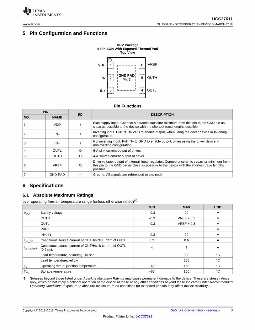
3 DescriptionThe UCC27611 is a single-channel, high-speed, gatedriver optimized for 5-V drive, specifically addressingenhancement mode GaN FETs. The drive voltageVREF is precisely controlled by internal linearregulator to 5 V. The UCC27611 offers asymmetricalrail-to-rail peak current drive capability with 4-Asource and 6-A sink. Split output configuration allowsindividual turnon and turnoff time optimizationdepending on FET. Package and pinout withminimum parasitic inductances reduce the rise andfall time and limit the ringing. Additionally, the shortpropagation delay with minimized tolerances andvariations allows efficient operation at highfrequencies. The 1-Ω and 0.35-Ω resistance boostsimmunity to hard switching with high slew rate dV anddt.
The independence from VDD input signal thresholdsensure TTL and CMOS low-voltage logiccompatibility. For safety reason, when the input pinsare in a floating condition, the internal input pullupand pulldown resistors hold the output LOW. Internalcircuitry on VREF pin provides an undervoltagelockout function that holds output LOW until VREFsupply voltage is within operating range. UCC27611is offered in a small 2.00 mm × 2.00 mm SON-6package (DRV) with exposed thermal and ground padthat improves the package power-handling capability.The UCC27611 operates over wide temperaturerange from –40°C to 140°C.
Device Information(1)
PART NUMBER PACKAGE BODY SIZE (NOM)UCC27611 SON (6) 2.00 mm × 2.00 mm
(1) For all available packages, see the orderable addendum atthe end of the datasheet.
Typical Application Diagram
2
UCC27611SLUSBA5F –DECEMBER 2012–REVISED MARCH 2018 www.ti.com
Product Folder Links: UCC27611
Submit Documentation Feedback Copyright © 2012–2018, Texas Instruments Incorporated
Table of Contents1 Features .................................................................. 12 Applications ........................................................... 13 Description ............................................................. 14 Revision History..................................................... 25 Pin Configuration and Functions ......................... 36 Specifications......................................................... 3
6.1 Absolute Maximum Ratings ...................................... 36.2 ESD Ratings.............................................................. 46.3 Recommended Operating Conditions....................... 46.4 Thermal Information .................................................. 46.5 Electrical Characteristics........................................... 56.6 Switching Characteristics .......................................... 56.7 Typical Characteristics .............................................. 7
7 Detailed Description .............................................. 87.1 Overview ................................................................... 87.2 Functional Block Diagram ......................................... 87.3 Feature Description................................................... 8
7.4 Device Functional Modes........................................ 118 Application and Implementation ........................ 12
8.1 Application Information............................................ 128.2 Typical Application ................................................. 13
9 Power Supply Recommendations ...................... 1810 Layout................................................................... 20
10.1 Layout Guidelines ................................................. 2010.2 Layout Example .................................................... 20
11 Device and Documentation Support ................. 2111.1 Documentation Support ........................................ 2111.2 Receiving Notification of Documentation Updates 2111.3 Community Resources.......................................... 2111.4 Trademarks ........................................................... 2111.5 Electrostatic Discharge Caution............................ 2111.6 Glossary ................................................................ 21
12 Mechanical, Packaging, and OrderableInformation ........................................................... 21
4 Revision HistoryNOTE: Page numbers for previous revisions may differ from page numbers in the current version.
Changes from Revision E (February 2018) to Revision F Page
• Changed Power Up (Noninverting Drive) graphic ................................................................................................................. 9• Changed Power Up (Inverting Drive) graphic......................................................................................................................... 9
Changes from Revision D (October 2017) to Revision E Page
• Changed title ......................................................................................................................................................................... 1
Changes from Revision C (December 2015) to Revision D Page
• Changed title ......................................................................................................................................................................... 1
Changes from Revision B (May 2013) to Revision C Page
• Added ESD Ratings table, Feature Description section, Device Functional Modes, Application and Implementationsection, Power Supply Recommendations section, Layout section, Device and Documentation Support section, andMechanical, Packaging, and Orderable Information section .................................................................................................. 1
Changes from Revision A (December 2012) to Revision B Page
• Added Electrical Characteristics Inputs (IN+, IN–) section values ......................................................................................... 5
4
5
61
2
3
VDD
IN+
VREF
GND PAD
Pin 7IN-
OUTL
OUTH
3
UCC27611www.ti.com SLUSBA5F –DECEMBER 2012–REVISED MARCH 2018
Product Folder Links: UCC27611
Submit Documentation FeedbackCopyright © 2012–2018, Texas Instruments Incorporated
5 Pin Configuration and Functions
DRV Package6-Pin SON With Exposed Thermal Pad
Top View
Pin FunctionsPIN
I/O DESCRIPTIONNO. NAME
1 VDD I Bias supply input. Connect a ceramic capacitor minimum from this pin to the GND pin asclose as possible to the device with the shortest trace lengths possible.
2 IN– I Inverting input. Pull IN+ to VDD to enable output, when using the driver device in Invertingconfiguration.
3 IN+ I Noninverting input. Pull IN– to GND to enable output, when using the driver device innoninverting configuration.
4 OUTL O 6-A sink current output of driver.5 OUTH O 4-A source current output of driver.
6 VREF ODrive voltage, output of internal linear regulator. Connect a ceramic capacitor minimum fromthis pin to the GND pin as close as possible to the device with the shortest trace lengthspossible.
7 GND PAD — Ground. All signals are referenced to this node.
(1) Stresses beyond those listed under Absolute Maximum Ratings may cause permanent damage to the device. These are stress ratingsonly, which do not imply functional operation of the device at these or any other conditions beyond those indicated under RecommendedOperating Conditions. Exposure to absolute-maximum-rated conditions for extended periods may affect device reliability.
6 Specifications
6.1 Absolute Maximum Ratingsover operating free-air temperature range (unless otherwise noted) (1)
MIN MAX UNITVDD Supply voltage –0.3 20 V
OUTH –0.3 VREF + 0.3 VOUTL –0.3 VREF + 0.3 VVREF 6 VIN+, IN– –0.3 20 V
Iout_DC Continuous source current of OUTH/sink current of OUTL 0.3 0.6 A
Iout_pulsedContinuous source current of OUTH/sink current of OUTL(0.5 µs), 4 6 A
Lead temperature, soldering, 10 sec. 300 °CLead temperature, reflow 260 °C
TJ Operating virtual junction temperature –40 150 °CTstg Storage temperature –65 150 °C
4
UCC27611SLUSBA5F –DECEMBER 2012–REVISED MARCH 2018 www.ti.com
Product Folder Links: UCC27611
Submit Documentation Feedback Copyright © 2012–2018, Texas Instruments Incorporated
(1) JEDEC document JEP155 states that 500-V HBM allows safe manufacturing with a standard ESD control process.(2) JEDEC document JEP157 states that 250-V CDM allows safe manufacturing with a standard ESD control process.
6.2 ESD RatingsVALUE UNIT
V(ESD) Electrostatic dischargeHuman-body model (HBM), per ANSI/ESDA/JEDEC JS-001 (1) ±2000
VCharged-device model (CDM), per JEDEC specification JESD22-C101 (2) ±500
6.3 Recommended Operating Conditionsover operating free-air temperature range (unless otherwise noted)
MIN NOM MAX UNITVDD Supply voltage 4 12 18 VIN Input voltage 0 18 V
IN+, IN– resistance 100 kΩTJ Operating junction temperature –40 140 °C
(1) For more information about traditional and new thermal metrics, see the Semiconductor and IC Package Thermal Metrics applicationreport.
6.4 Thermal Information
THERMAL METRIC (1)UCC27611
UNITDRV (SON)6 PINS
RθJA Junction-to-ambient thermal resistance 80.3 °C/WRθJC(top) Junction-to-case (top) thermal resistance 11.9 °C/WRθJB Junction-to-board thermal resistance 49.7 °C/WψJT Junction-to-top characterization parameter 5.5 °C/WψJB Junction-to-board characterization parameter 50.1 °C/WRθJC(bot) Junction-to-case (bottom) thermal resistance 18.8 °C/W
5
UCC27611www.ti.com SLUSBA5F –DECEMBER 2012–REVISED MARCH 2018
Product Folder Links: UCC27611
Submit Documentation FeedbackCopyright © 2012–2018, Texas Instruments Incorporated
(1) Device operational with output switching.(2) Ensured by design, not tested in production.
6.5 Electrical CharacteristicsVDD = 12 V, TA = TJ = –40 °C to 140 °C, 2-µF capacitor from VDD to GND and from VREF to GND. Currents are positiveinto, negative out of the specified terminal. OUTH and OUTL are tied together. (unless otherwise noted) (1)
PARAMETER TEST CONDITIONS MIN TYP MAX UNITBIAS CURRENT
IDD(off) Start-up currentVDD = 3, IN+ = VDD,IN– = GND 100 180
μAIN+ = GND, IN– = VDD 75 160
UNDER VOLTAGE LOCKOUT (UVLO)VDD(on) Supply start threshold 3.55 3.8 4.15 V
VDD(off)Minimum operating voltage after supplystart 3.3 3.55 3.9 V
VDD_H Supply voltage hysteresis 0.25 VINPUTS (IN+, IN–)
VIN_L Input signal low threshold Output high for IN– pin,Output Low for IN+ pin 0.9 1.1 1.3 V
VIN_H Input signal high threshold Output high for IN+ pin,Output low for IN– pin 1.85 2.05 2.25 V
VIN_HYS Input signal hysteresis 0.7 0.95 1.2 VVREF
VREF VREF regulator output 4.75 5 5.15 VVREF_line VREF line regulation VDD from 6 V to 18 V 0.05 VVREF_load VREF load regulation IR from 0 mA to 50 mA 0.075 VISCC Short circuit current –90 –75 –60 mAOUTPUTS (OUTH/OUTL AND OUT)
ISRC/SNKSource peak current (OUTH) / sink peakcurrent (OUTL) (2) CLOAD = 0.22 µF, FSW = 1 kHz, (2) –4/+6 A
VOH OUTH high voltage IOUTH = –10 mA VDD–0.05 V
VOL OUTL low voltage IOUTL = 10 mA 0.02 V
ROH OUTH pullup resistance
TA = 25 °C,IOUT = –25 mA to –50 mA 1
ΩTA = –40 °C to 140 °C,IOUT = –50 mA 2
ROL OUTH pulldown resistance
TA = 25 °C,IOUT = 25 mA to 50 mA 0.35
ΩTA = –40°C to 140°C,IOUT = 50 mA 1.5
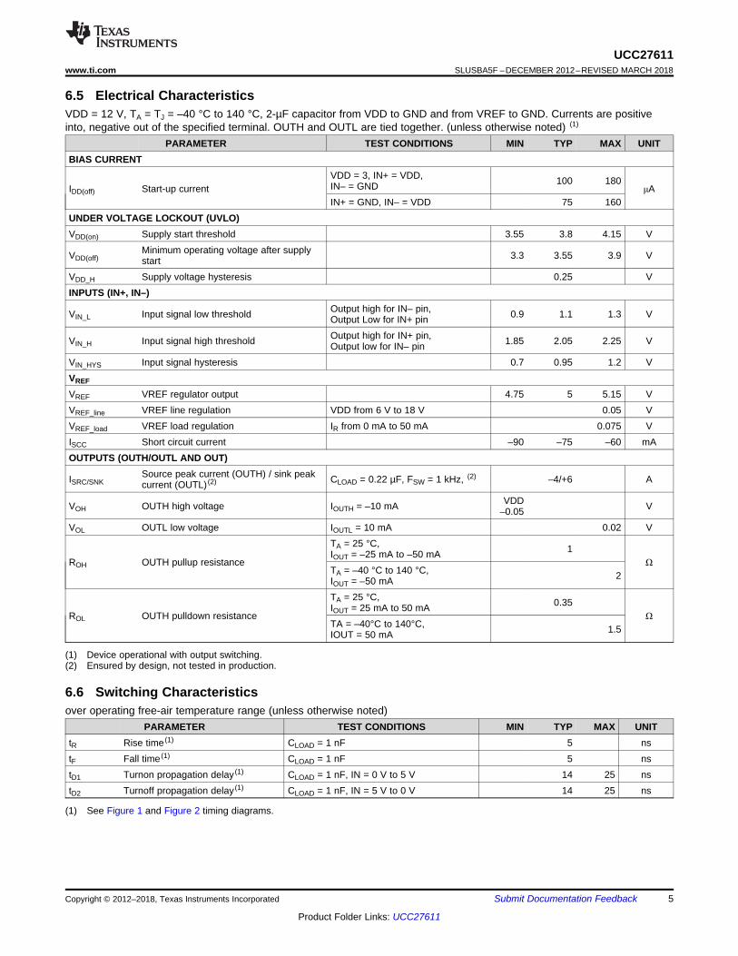
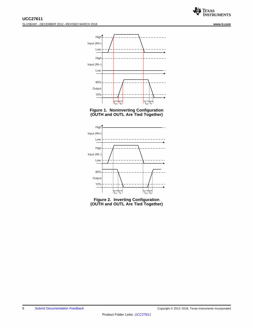
(1) See Figure 1 and Figure 2 timing diagrams.
6.6 Switching Characteristicsover operating free-air temperature range (unless otherwise noted)
PARAMETER TEST CONDITIONS MIN TYP MAX UNITtR Rise time (1) CLOAD = 1 nF 5 nstF Fall time (1) CLOAD = 1 nF 5 nstD1 Turnon propagation delay (1) CLOAD = 1 nF, IN = 0 V to 5 V 14 25 nstD2 Turnoff propagation delay (1) CLOAD = 1 nF, IN = 5 V to 0 V 14 25 ns
Output
90%
10%
Input (IN–)
High
Low
Input (IN+)
High
Low
tD1 tF tD2 tR
Output
90%
10%
Input (IN–)
High
Low
Input (IN+)
High
Low
tD1 tR tD2 tF
6
UCC27611SLUSBA5F –DECEMBER 2012–REVISED MARCH 2018 www.ti.com
Product Folder Links: UCC27611
Submit Documentation Feedback Copyright © 2012–2018, Texas Instruments Incorporated
Figure 1. Noninverting Configuration(OUTH and OUTL Are Tied Together)
Figure 2. Inverting Configuration(OUTH and OUTL Are Tied Together)
5
5.2
5.4
5.6
5.8
6
−50 0 50 100 150
Temperature (°C)
Ris
eT
ime
(n
s)
VDD = 12 V
CLoad = 1.8nF
G001
5
5.2
5.4
5.6
5.8
6
−50 0 50 100 150
Temperature (°C)
Fa
llT
ime
(n
s)
VDD = 12 V
CLoad = 1.8nF
G001
10
12
14
16
18
20
−50 0 50 100 150
Temperature (°C)
IN−
Pro
pa
ga
tio
n D
ela
y (
ns)
Turn−On
Turn−Off
VDD = 12 V
G001
0.2
0.3
0.4
−50 0 50 100 150
Temperature (°C)
UV
LO
Hyste
rsis
(V
)
UVLO Hysterisis
G001
4.8
4.9
5
−50 0 50 100 150
Temperature (°C)
VR
EF
(V
)
G001
8
10
12
14
16
18
−50 0 50 100 150
Temperature (°C)
IN+
Pro
pa
ga
tio
n D
ela
y (
ns)
Turn−On
Turn−Off
VDD = 12 V
G001
7
UCC27611www.ti.com SLUSBA5F –DECEMBER 2012–REVISED MARCH 2018
Product Folder Links: UCC27611
Submit Documentation FeedbackCopyright © 2012–2018, Texas Instruments Incorporated
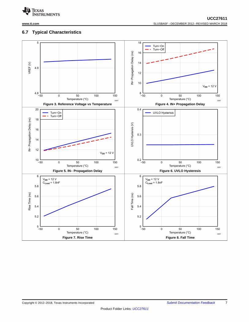
6.7 Typical Characteristics
Figure 3. Reference Voltage vs Temperature Figure 4. IN+ Propagation Delay
Figure 5. IN– Propagation Delay Figure 6. UVLO Hysteresis
Figure 7. Rise Time Figure 8. Fall Time
VDD UVLO
VDDVREF VREF
VDD
3
2
1
7
4
5
6
VREF
LDO
IN-
IN+
VREF
OUTH
OUTL
GND
8
UCC27611SLUSBA5F –DECEMBER 2012–REVISED MARCH 2018 www.ti.com
Product Folder Links: UCC27611
Submit Documentation Feedback Copyright © 2012–2018, Texas Instruments Incorporated
7 Detailed Description
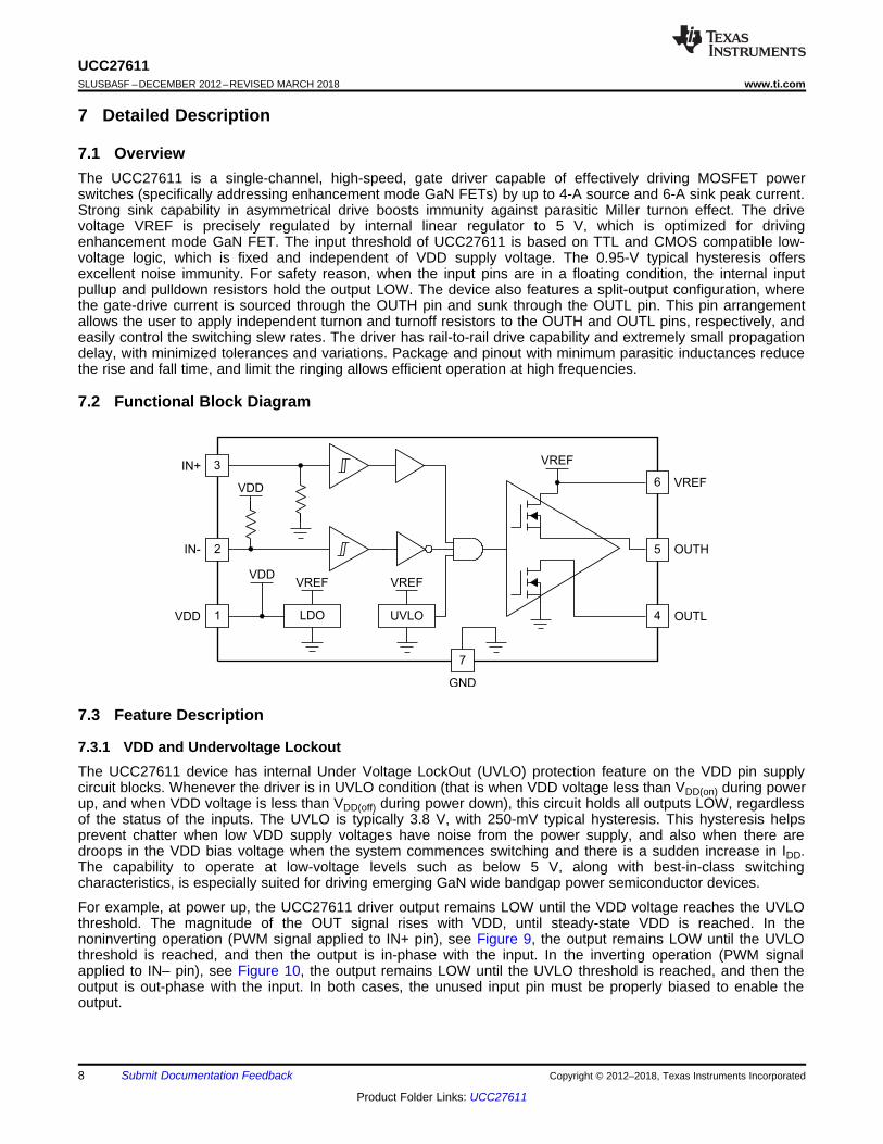
7.1 OverviewThe UCC27611 is a single-channel, high-speed, gate driver capable of effectively driving MOSFET powerswitches (specifically addressing enhancement mode GaN FETs) by up to 4-A source and 6-A sink peak current.Strong sink capability in asymmetrical drive boosts immunity against parasitic Miller turnon effect. The drivevoltage VREF is precisely regulated by internal linear regulator to 5 V, which is optimized for drivingenhancement mode GaN FET. The input threshold of UCC27611 is based on TTL and CMOS compatible low-voltage logic, which is fixed and independent of VDD supply voltage. The 0.95-V typical hysteresis offersexcellent noise immunity. For safety reason, when the input pins are in a floating condition, the internal inputpullup and pulldown resistors hold the output LOW. The device also features a split-output configuration, wherethe gate-drive current is sourced through the OUTH pin and sunk through the OUTL pin. This pin arrangementallows the user to apply independent turnon and turnoff resistors to the OUTH and OUTL pins, respectively, andeasily control the switching slew rates. The driver has rail-to-rail drive capability and extremely small propagationdelay, with minimized tolerances and variations. Package and pinout with minimum parasitic inductances reducethe rise and fall time, and limit the ringing allows efficient operation at high frequencies.
7.2 Functional Block Diagram
7.3 Feature Description
7.3.1 VDD and Undervoltage LockoutThe UCC27611 device has internal Under Voltage LockOut (UVLO) protection feature on the VDD pin supplycircuit blocks. Whenever the driver is in UVLO condition (that is when VDD voltage less than VDD(on) during powerup, and when VDD voltage is less than VDD(off) during power down), this circuit holds all outputs LOW, regardlessof the status of the inputs. The UVLO is typically 3.8 V, with 250-mV typical hysteresis. This hysteresis helpsprevent chatter when low VDD supply voltages have noise from the power supply, and also when there aredroops in the VDD bias voltage when the system commences switching and there is a sudden increase in IDD.The capability to operate at low-voltage levels such as below 5 V, along with best-in-class switchingcharacteristics, is especially suited for driving emerging GaN wide bandgap power semiconductor devices.
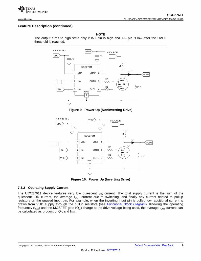
For example, at power up, the UCC27611 driver output remains LOW until the VDD voltage reaches the UVLOthreshold. The magnitude of the OUT signal rises with VDD, until steady-state VDD is reached. In thenoninverting operation (PWM signal applied to IN+ pin), see Figure 9, the output remains LOW until the UVLOthreshold is reached, and then the output is in-phase with the input. In the inverting operation (PWM signalapplied to IN– pin), see Figure 10, the output remains LOW until the UVLO threshold is reached, and then theoutput is out-phase with the input. In both cases, the unused input pin must be properly biased to enable theoutput.
1
2
3
6
5
4
VDD
IN-
IN+
VREF
OUTH
OUTL
UCC27611
R1
R2
Q1
VREF
D1
C1
+
VOUT
VSOURCE
L1
C3
VREF4.5 V to 18 V
C2
VDD
IN-
7
GND
1
2
3
6
5
4
VDD
IN-
IN+
VREF
OUTH
OUTL
UCC27611
R1
R2
Q1
IN+
D1
C1
+
VOUT
VSOURCE
L1
C3
VREF4.5 V to 18 V
C2
VDD
7
GND
9
UCC27611www.ti.com SLUSBA5F –DECEMBER 2012–REVISED MARCH 2018
Product Folder Links: UCC27611
Submit Documentation FeedbackCopyright © 2012–2018, Texas Instruments Incorporated
Feature Description (continued)
NOTEThe output turns to high state only if IN+ pin is high and IN– pin is low after the UVLOthreshold is reached.
Figure 9. Power Up (Noninverting Drive)
Figure 10. Power Up (Inverting Drive)
7.3.2 Operating Supply CurrentThe UCC27611 device features very low quiescent IDD current. The total supply current is the sum of thequiescent IDD current, the average IOUT current due to switching, and finally any current related to pullupresistors on the unused input pin. For example, when the inverting input pin is pulled low, additional current isdrawn from VDD supply through the pullup resistors (see Functional Block Diagram). Knowing the operatingfrequency (fSW) and the MOSFET gate (QG) charge at the drive voltage being used, the average IOUT current canbe calculated as product of QG and fSW.

VREF
ROH
ROL
Gate
Voltage
Boost
Narrow Pulse at
each Turn On
Anti Shoot -
Through
Circuitry
Input Signal
RNMOS, Pull Up
OUTL
OUTH
10
UCC27611SLUSBA5F –DECEMBER 2012–REVISED MARCH 2018 www.ti.com
Product Folder Links: UCC27611
Submit Documentation Feedback Copyright © 2012–2018, Texas Instruments Incorporated
Feature Description (continued)7.3.3 Input StageThe input pins of the UCC27611 device is based on a TTL and CMOS compatible input threshold logic that isindependent of the VDD supply voltage. With typical high threshold = 2.05 V and typical low threshold = 1.1 V,the logic level thresholds can be conveniently driven with PWM control signals derived from 3.3-V and 5-V digitalpower controllers. Wider hysteresis (typical 1 V) offers enhanced noise immunity compared to traditional TTLlogic implementations, where the hysteresis is typically less than 0.5 V. These devices also feature tight controlof the input pin threshold voltage levels, which eases system design considerations, and ensures stableoperation across temperature. The very low input capacitance on these pins reduces loading, and increasesswitching speed.
The device features an important safety function wherein, whenever any of the input pins are in a floatingcondition, the output of the respective channel is held in the low state. This is achieved using VDD pullupresistors on all the inverting inputs (IN– pin), or GND pulldown resistors on all the noninverting input pins (IN+pin)(see Functional Block Diagram).
The device also features a dual input configuration, with two input pins available to control the state of the output.The user has the flexibility to drive the device using either a noninverting input pin (IN+), or an inverting input pin(IN–). The state of the output pin is dependent on the bias of both the IN+ and IN– pins. See Table 1 input andoutput logic truth table, and the Figure 12 for additional clarification.
7.3.4 Enable FunctionAn enable and disable function can be easily implemented in the UCC27611 device using the unused input pin.When IN+ is pulled down to GND, or IN– is pulled down to VDD, the output is disabled. Thus, IN+ pin can beused like an enable pin that is based on active high logic, while IN– can be used like an enable pin that is basedon active low logic.
7.3.5 Output StageThe output stage of the UCC27611 device is illustrated in Figure 11. OUTH and OUTL are externally connectedand pinned out as OUTH and OUTL pins. The UCC27611 device features a unique architecture on the outputstage, which delivers the highest peak source current when it is most needed during the Miller plateau region ofthe power switch turnon transition (when the power switch drain and collector voltage experiences dV and dt).The device output stage features a hybrid pullup structure using a parallel arrangement of N-channel and P-channel MOSFET devices. By turning on the N-channel MOSFET, during a narrow instant when the outputchanges state from low to high, the gate-driver device is able to deliver a brief boost in the peak-sourcing current,enabling fast turnon.
Figure 11. UCC27611 Device Gate Driver Output Structure
11
UCC27611www.ti.com SLUSBA5F –DECEMBER 2012–REVISED MARCH 2018
Product Folder Links: UCC27611
Submit Documentation FeedbackCopyright © 2012–2018, Texas Instruments Incorporated
Feature Description (continued)The ROH parameter (see Electrical Characteristics) is a DC measurement, and it is representative of the on-resistance of the P-channel device only, because the N-channel device is turned on only during output change ofstate from low to high. Thus, the effective resistance of the hybrid pullup stage is much lower than what isrepresented by ROH parameter. The pulldown structure is composed of a N-channel MOSFET only. The ROLparameter (see Electrical Characteristics), which is also a DC measurement, is representative of true impedanceof the pulldown stage in the device.
The driver output voltage swings between VDD and GND, providing rail-to-rail operation thanks to the MOSoutput stage that delivers very low dropout. The presence of the MOSFET body diodes also offers lowimpedance to switching overshoots and undershoots. This means that in many cases, external Schottky diodeclamps may be eliminated. The outputs of these drivers are designed to withstand 500-mA reverse currentwithout either damage to the device, or logic malfunction.
7.3.6 Low Propagation DelaysThe UCC27611 driver device feature best-in-class input-to-output propagation delay of 14 ns (typical) at VDD =12 V. This promises the lowest level of pulse transmission distortion available from industry standard gate-driverdevices for high-frequency switching applications. There is very little variation of the propagation delay withtemperature and supply voltage as well, offering typically less than 20-ns propagation delays across the entirerange of application conditions.
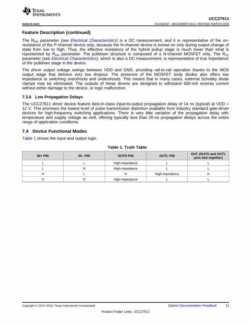
7.4 Device Functional ModesTable 1 shows the input and output logic.
Table 1. Truth Table
IN+ PIN IN– PIN OUTH PIN OUTL PIN OUT (OUTH and OUTLpins tied together)
L L High-impedance L LL H High-impedance L LH L H High-impedance HH H High-impedance L L
12
UCC27611SLUSBA5F –DECEMBER 2012–REVISED MARCH 2018 www.ti.com
Product Folder Links: UCC27611
Submit Documentation Feedback Copyright © 2012–2018, Texas Instruments Incorporated
8 Application and Implementation
NOTEInformation in the following applications sections is not part of the TI componentspecification, and TI does not warrant its accuracy or completeness. TI’s customers areresponsible for determining suitability of components for their purposes. Customers mustvalidate and test their design implementation to confirm system functionality.
8.1 Application InformationHigh-current gate-driver devices are required in switching power applications for a variety of reasons. To effectthe fast switching of power devices, and reduce associated switching-power losses, a powerful gate-driver deviceemploys between the PWM output of control devices and the gates of the power semiconductor devices. Further,gate-driver devices are indispensable when it is not feasible for the PWM controller device to directly drive thegates of the switching devices. With the advent of digital power, this situation is often encountered because thePWM signal from the digital controller is often a 3.3-V logic signal that is not capable of effectively turning on apower switch. A level-shifting circuitry is required to boost the 3.3-V signal to the gate-drive voltage to fully turn-on the power device and minimize conduction losses. Traditional buffer-drive circuits based on NPN/PNP bipolartransistors in a totem-pole arrangement, as emitter-follower configurations, prove inadequate with digital powerbecause the traditional buffer-drive circuits lack level-shifting capability. Gate-driver devices effectively combineboth the level-shifting and buffer-drive functions. Gate-driver devices also find other needs such as minimizingthe effect of high-frequency switching noise by locating the high-current driver physically close to the powerswitch, driving gate-drive transformers and controlling floating power-device gates, reducing power dissipationand thermal stress in controller devices by moving gate-charge power losses into the controller.

1
2
3
6
5
4
VDD
IN-
IN+
VREF
OUTH
OUTL
UCC27611
R1
R2
Q1
IN+
D1
C1
+
VOUT
VSOURCE
L1
C3
VREF4.5 V to 18 V
C2
VDD
7
GND
1
2
3
6
5
4
VDD
IN-
IN+
VREF
OUTH
OUTL
UCC27611
R1
R2
Q1
VREF
D1
C1
+
VOUT
VSOURCE
L1
C3
VREF4.5 V to 18 V
C2
VDD
IN-
7
GND
13
UCC27611www.ti.com SLUSBA5F –DECEMBER 2012–REVISED MARCH 2018
Product Folder Links: UCC27611
Submit Documentation FeedbackCopyright © 2012–2018, Texas Instruments Incorporated
8.2 Typical Application
Figure 12. UCC27611 Driving Enhancement Mode GaN FET in Boost Configuration
8.2.1 Design RequirementsThe requirements of gate-driver for driving enhancement mode GaN FET are listed as below:• The headroom between the recommended gate-drive voltage and the absolute maximum rating of GaN
transistor is generally marginal. It is critical to drive the GaN FET by an accurate gate-drive supply voltage• The turnon threshold of the GaN transistor is generally much lower than that of silicon MOSFETs, the risk of
Miller turnon and shoot-through becomes a concern for the higher-voltage devices. Low pulldown impedanceis necessary to boost the immunity of Miller turnon
• With enhancement mode GaN transistors, the need for minimizing pulldown impedance means that additionpulldown gate resistor and antiparallel diode connection is not recommended. Split the gate pullup andpulldown connections and allow the insertion of external pullup resistance for EMI and voltage-overshootcontrol is needed
• At high switching speeds, the impact of the gate-drive interconnection impedance becomes important, low-inductance packages with good thermal capability is required for gate driver
14
UCC27611SLUSBA5F –DECEMBER 2012–REVISED MARCH 2018 www.ti.com
Product Folder Links: UCC27611
Submit Documentation Feedback Copyright © 2012–2018, Texas Instruments Incorporated
Typical Application (continued)8.2.2 Detailed Design Procedure
8.2.2.1 Gate Drive Supply VoltageThe drive voltage for GaN FETs must be tightly regulated, that’s why a linear regulator is integrated inUCC27611 to providing well-regulated 5-V voltage (VREF). Depending on layout and noise generated by thepower stage, the parasitic inductance in conjunction with the Miller capacitance of the FET can cause excessiveringing on the gate drive waveform resulting in peaks higher that the regulated VREF drive voltage. With enoughenergy present, the potential exists to charge the VREF decoupling capacitor higher than the 6-V maximumallowed on a Gallium Nitride transistor. To prevent this from happening, the driver must be close to its own FETto avoid excessive ringing during fast switching transitions, and external gate resistor RGH connected to OUTHpin of driver must be used to limit the turnon speed.
8.2.2.2 Input ConfigurationThe UCC27611 offers both inverting (IN–) and noninverting (IN+) inputs to satisfy requirements for inverting andnoninverting gate drive in a single device type. The design must specify what type of input-to-output configurationmust be used. If turning on the power MOSFET when the input signal is in high state is preferred, then a devicecapable of the noninverting configuration must be selected. If turning off the power MOSFET when the inputsignal is in high state is preferred, then a device capable of the inverting configuration must be chosen. Once aninput pin has been chosen for PWM drive, the other input pin (the unused input pin) must be properly biased toenable the output. The unused input pin cannot remain in a floating condition, because whenever any input pin isleft in a floating condition, the output is disabled for safety purposes. Alternatively, the unused input pin caneffectively be used to implement an enable and disable function, as explained below.• To drive the device in a noninverting configuration, apply the PWM control input signal to IN+ pin. In this
case, the unused input pin, IN–, must be biased low (tied to GND) to enable the output. Alternately, the IN–pin can be used to implement the enable and disable function using an external logic signal. OUT is disabledwhen IN– is biased high and OUT is enabled when IN– is biased low
• To drive the device in an inverting configuration, apply the PWM control input signal to IN– pin. In this case,the unused input pin, IN+, must be biased high (For example, tied to VDD) to enable the output. Alternately,the IN+ pin can be used to implement the enable and disable function using an external logic signal. OUT isdisabled when IN+ is biased low and OUT is enabled when IN+ is biased high
NOTEThe output pin can be driven into a high state only when IN+ pin is biased high and IN–input is biased low. See Device Functional Modes for information on device functionality.
The input stage of the driver must preferably be driven by a signal with a short rise or fall time. Take carewhenever the driver is used with slowly varying input signals, especially in situations where the device is locatedin a mechanical socket, or PCB layout is not optimal. High dI/dt current from the driver output coupled with boardlayout parasitic can cause ground bounce. Because the device features just one GND pin, which may bereferenced to the power ground, this may modify the differential voltage between input pins and GND and triggeran unintended change of output state. Because of fast 13-ns propagation delay, this can ultimately result in high-frequency oscillations, which increase power dissipation and pose risk of damage. In the worst case, when aslow input signal is used and PCB layout is not optimal, it may be necessary to add a small capacitor betweeninput pin and ground very close to the driver device. This helps to convert the differential mode noise withrespect to the input logic circuitry into common mode noise and avoid unintended change of output state.
DISS DC SWP P P= +
Gate Driver
ROL
RG
CGD
CGS
COSS
VDS VIN
ISNK
VIN
VTH
ON OFF
Miller Turn -On Spike in V GS
VDS of
MOSFET
VGS of
MOSFET
15
UCC27611www.ti.com SLUSBA5F –DECEMBER 2012–REVISED MARCH 2018
Product Folder Links: UCC27611
Submit Documentation FeedbackCopyright © 2012–2018, Texas Instruments Incorporated
Typical Application (continued)8.2.2.3 Output ConfigurationGenerally, the switching speed of the power switch during turnon and turnoff must be as fast as possible tominimize switching power losses. The gate driver device must be able to provide the required peak current forachieving the targeted switching speeds for the targeted power MOSFET. In practical designs, the parasitic traceinductance in the gate drive circuit of the PCB has a definitive role to play on the power MOSFET switchingspeed. The effect of this trace inductance is to limit the dI/dt of the output current pulse of the gate driver.Because of this, the desired switching speed may not be realized, even when theoretical calculations indicate thegate driver can achieve the targeted switching speed. Thus, placing the gate driver device very close to thepower MOSFET and designing a tight gate drive-loop with minimal PCB trace inductance is important to realizethe full peak-current capability of the gate driver.
The UCC27611 is capable of delivering 4-A source, 6-A sink (asymmetrical drive) at VDD = 12 V. Strong sinkcapability in asymmetrical drive results in a very low pulldown impedance in the driver output stage which boostsimmunity against parasitic, Miller turnon (C × dV/dt turnon) effect, especially where low gate-charge MOSFETs oremerging wide band-gap GaN power switches are used.
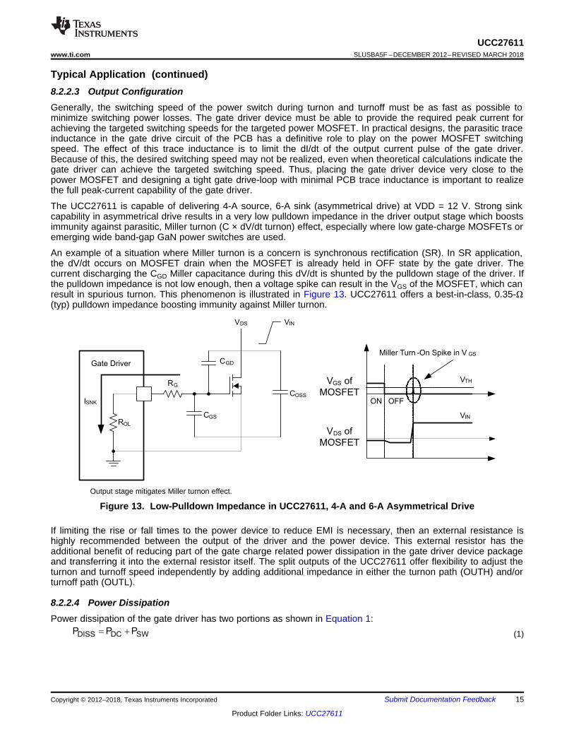
An example of a situation where Miller turnon is a concern is synchronous rectification (SR). In SR application,the dV/dt occurs on MOSFET drain when the MOSFET is already held in OFF state by the gate driver. Thecurrent discharging the CGD Miller capacitance during this dV/dt is shunted by the pulldown stage of the driver. Ifthe pulldown impedance is not low enough, then a voltage spike can result in the VGS of the MOSFET, which canresult in spurious turnon. This phenomenon is illustrated in Figure 13. UCC27611 offers a best-in-class, 0.35-Ω(typ) pulldown impedance boosting immunity against Miller turnon.
Output stage mitigates Miller turnon effect.
Figure 13. Low-Pulldown Impedance in UCC27611, 4-A and 6-A Asymmetrical Drive
If limiting the rise or fall times to the power device to reduce EMI is necessary, then an external resistance ishighly recommended between the output of the driver and the power device. This external resistor has theadditional benefit of reducing part of the gate charge related power dissipation in the gate driver device packageand transferring it into the external resistor itself. The split outputs of the UCC27611 offer flexibility to adjust theturnon and turnoff speed independently by adding additional impedance in either the turnon path (OUTH) and/orturnoff path (OUTL).
8.2.2.4 Power DissipationPower dissipation of the gate driver has two portions as shown in Equation 1:
(1)
ON OFFSW G REF SW
ON GH OFF GL
R RP Q V f
R R R R
æ ö= ´ ´ +ç ÷
+ +è ø
2G LOAD REF SW G REF SWP C V f Q V f= ´ ´ = ´ ´
2G LOAD REF SWP C V f= ´ ´
2G LOAD REF
1E C V
2= ´ ´
16
UCC27611SLUSBA5F –DECEMBER 2012–REVISED MARCH 2018 www.ti.com
Product Folder Links: UCC27611
Submit Documentation Feedback Copyright © 2012–2018, Texas Instruments Incorporated
Typical Application (continued)The DC portion of the power dissipation is PDC = IQ × VDD where IQ is the quiescent current for the driver. Thequiescent current is the current consumed by the device to bias all internal circuits such as input stage, referencevoltage, logic circuits, protections, and so forth and also any current associated with switching of internal deviceswhen the driver output changes state (such as charging and discharging of parasitic capacitances, parasiticshoot-through and so forth). The UCC27611 device features very low quiescent currents (see ElectricalCharacteristics) and contains internal logic to eliminate any shoot-through in the output driver stage. Thus, theeffect of the PDC on the total power dissipation within the gate driver can be safely assumed to be negligible.
The power dissipated in the gate-driver package during switching (PSW) depends on the following factors:• Gate charge required of the power device (usually a function of the drive voltage VG, which is very close to
input bias supply voltage VREF due to low VOH dropout)• Switching frequency• Use of external gate resistors
When a driver device is tested with a discrete, capacitive load it is a fairly simple matter to calculate the powerthat is required from the bias supply. The energy that must be transferred from the bias supply to charge thecapacitor is given by Equation 2:
where• CLOAD is load capacitor of driver. (2)
There is an equal amount of energy dissipated when the capacitor is charged. This leads to a total power lossgiven by Equation 3.
where• fSW is the switching frequency. (3)
The switching load presented by a power MOSFET and IGBT can be converted to an equivalent capacitance byexamining the gate charge required to switch the device. This gate charge includes the effects of the inputcapacitance plus the added charge needed to swing the drain voltage of the power device as it switches betweenthe ON and OFF states. Most manufacturers provide specifications of typical and maximum gate charge, in nC,to switch the device under specified conditions. Using the gate charge QG, one can determine the power thatmust be dissipated when charging a capacitor. This is done by using the equation, QG = CLOAD × VREF, to provideEquation 4 for power:
(4)
This power PG is dissipated in the resistive elements of the circuit when the MOSFET or IGBT is being turned onor off. Half of the total power is dissipated when the load capacitor is charged during turnon, and the other half isdissipated when the load capacitor is discharged during turnoff. When no external gate resistor is employedbetween the driver and MOSFET and IGBT, this power is completely dissipated inside the driver package. Withthe use of external gate-drive resistors, the power dissipation is shared between the internal resistance of driverand external gate resistor in accordance to the ratio of the resistances (more power dissipated in the higherresistance component). Based on this simplified analysis, the driver power dissipation during switching iscalculated as Equation 5:
where• ROFF = ROL and RON = 2.7 × ROL (effective resistance of pullup structure).• RGH and RGL is external gate resistors connect to the OUTH and OUTL pins respective. (5)
17
UCC27611www.ti.com SLUSBA5F –DECEMBER 2012–REVISED MARCH 2018
Product Folder Links: UCC27611
Submit Documentation FeedbackCopyright © 2012–2018, Texas Instruments Incorporated
Typical Application (continued)8.2.2.5 Thermal ConsiderationsThe useful range of a driver is greatly affected by the drive power requirements of the load and the thermalcharacteristics of the package. In order for a gate driver to be useful over a particular temperature range, thepackage must allow for the efficient removal of the heat produced while keeping the junction temperature withinrated limits. The thermal metrics for the driver package is summarized in the Thermal Information of thedatasheet. The θJA metric must be used for comparison of power dissipation between different packages. The ψJTand ψJB metrics must be used when estimating the die temperature during actual application measurements. Fordetailed information regarding the thermal information table, please see the Application Note from TexasInstruments entitled, Semiconductor and IC Package Thermal Metrics IC Package Thermal Metrics (SPRA953).
The UCC27611 device includes a 6-pin DRV package with exposed thermal pad. The exposed thermal pad inDRV package provides designers with an ability to create an excellent heat removal sub-system from the vicinityof the device, thus helping to maintain a lower junction temperature. This pad must be soldered to the copper onthe printed circuit board directly underneath the device package. Then a printed circuit-board designed withthermal lands and thermal vias completes a very efficient heat removal subsystem. In such a design, the heat isextracted from the semiconductor junction through the thermal pad, which is then efficiently conducted away fromthe location of the device on the PCB through the thermal network. This helps to maintain a lower boardtemperature near the vicinity of the device leading to an overall lower device junction temperature.
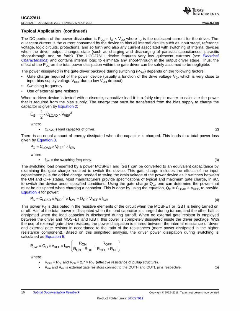
8.2.3 Application Curves
Figure 14. Output Rising(Ch1 = IN+, Ch2 = OUTPUT)
Figure 15. Output Falling(Ch1 = IN+, Ch2 = OUTPUT)
1
2
3
6
5
4
VDD
IN-
IN+
VREF
OUTH
OUTL
UCC27611
7
GND
Q1
18
UCC27611SLUSBA5F –DECEMBER 2012–REVISED MARCH 2018 www.ti.com
Product Folder Links: UCC27611
Submit Documentation Feedback Copyright © 2012–2018, Texas Instruments Incorporated
9 Power Supply RecommendationsThe bias supply voltage range for which the device is rated to operate is from 4 V to 18 V. The lower end of thisrange is governed by the internal under voltage-lockout (UVLO) protection feature on the VDD pin supply circuitblocks. Whenever the driver is in UVLO condition when the VDD pin voltage is below the VDD(on) supply startthreshold, this feature holds the output low, regardless of the status of the inputs. The upper end of this range isdriven by the 20-V absolute maximum voltage rating of the VDD pin of the device (which is a stress rating).Keeping a 2-V margin to allow for transient voltage spikes, the maximum recommended voltage for the VDD pinis 18V.
The UVLO protection feature also involves a hysteresis function. This means that when the VDD pin bias voltagehas exceeded the threshold voltage and device begins to operate, and if the voltage drops, then the devicecontinues to deliver normal functionality unless the voltage drop exceeds the hysteresis specification VDD(off).Therefore, ensuring that, while operating at or near the 4-V range, the voltage ripple on the auxiliary powersupply output is smaller than the hysteresis specification of the device is important to avoid triggering deviceshutdown.
During system shutdown, the device operation continues until the VDD pin voltage has dropped below thethreshold VDD(off) which must be accounted for while evaluating system shutdown timing design requirements.Likewise, at system startup, the device does not begin operation until the VDD pin voltage has exceeded abovethe VDD(on) threshold.
Because the driver draws current from the VDD pin to bias all internal circuits, for the best high-speed circuitperformance, two VDD bypass capacitors are recommended to prevent noise problems. The use of surfacemount components is highly recommended. A 0.1-μF ceramic capacitor must be located as close as possible tothe VDD to GND pins of the gate driver. In addition, a larger capacitor (such as 1-μF) with relatively low ESRmust be connected in parallel and close proximity to help deliver the high-current peaks required by the load. Theparallel combination of capacitors must present a low impedance characteristic for the expected current levelsand switching frequencies in the application.
The UCC27611 integrate a LDO to provide well-regulated voltage (VREF) to driving GaN FET. The charge forsource current pulses delivered by the OUTH pin is supplied through the VREF pin. As a result, every time acurrent is sourced out of the OUTH pin a corresponding current pulse is delivered into the device through theVREF pin. Thus ensuring that a local bypass capacitor is provided between the VREF and GND pins and locatedas close to the device as possible for the purpose of decoupling is important. A low ESR, ceramic surface mountcapacitor is necessary.
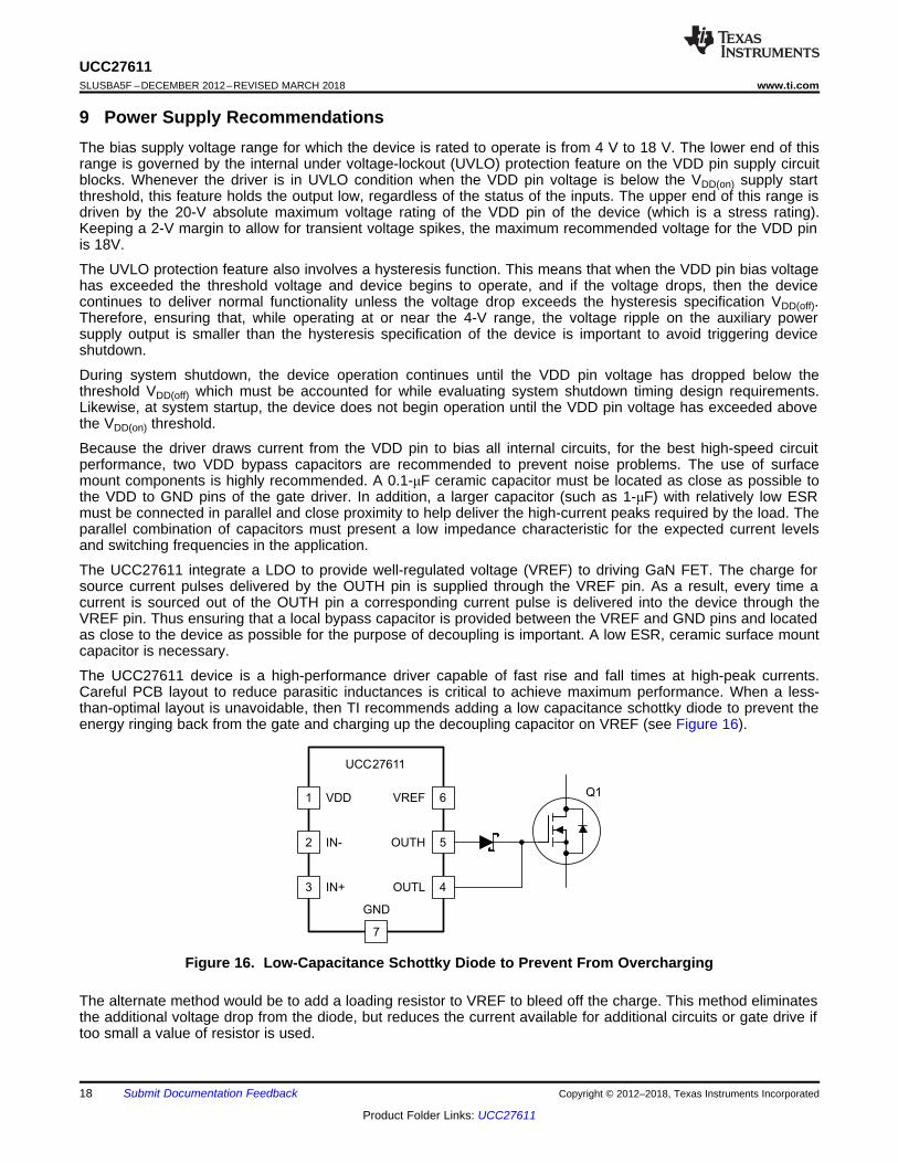
The UCC27611 device is a high-performance driver capable of fast rise and fall times at high-peak currents.Careful PCB layout to reduce parasitic inductances is critical to achieve maximum performance. When a less-than-optimal layout is unavoidable, then TI recommends adding a low capacitance schottky diode to prevent theenergy ringing back from the gate and charging up the decoupling capacitor on VREF (see Figure 16).
Figure 16. Low-Capacitance Schottky Diode to Prevent From Overcharging
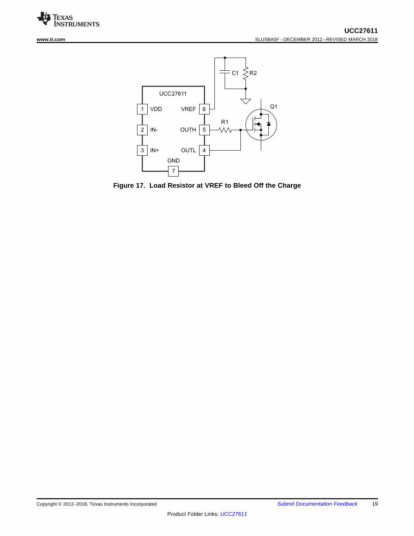
The alternate method would be to add a loading resistor to VREF to bleed off the charge. This method eliminatesthe additional voltage drop from the diode, but reduces the current available for additional circuits or gate drive iftoo small a value of resistor is used.
1
2
3
6
5
4
VDD
IN-
IN+
VREF
OUTH
OUTL
UCC27611
7
GND
Q1
R1
C1 R2
19
UCC27611www.ti.com SLUSBA5F –DECEMBER 2012–REVISED MARCH 2018
Product Folder Links: UCC27611
Submit Documentation FeedbackCopyright © 2012–2018, Texas Instruments Incorporated
Figure 17. Load Resistor at VREF to Bleed Off the Charge
GaN
G
VD
D IN±
IN+
CC
R
VR
EF
OU
TH
OU
TL
D S D S D S D S D
1 2 3
6 5 4
Substrate
GN
D P
AD
20
UCC27611SLUSBA5F –DECEMBER 2012–REVISED MARCH 2018 www.ti.com
Product Folder Links: UCC27611
Submit Documentation Feedback Copyright © 2012–2018, Texas Instruments Incorporated
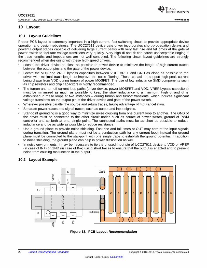
10 Layout
10.1 Layout GuidelinesProper PCB layout is extremely important in a high-current, fast-switching circuit to provide appropriate deviceoperation and design robustness. The UCC27611 device gate driver incorporates short-propagation delays andpowerful output stages capable of delivering large current peaks with very fast rise and fall times at the gate ofpower switch to facilitate voltage transitions very quickly. Very high di and dt can cause unacceptable ringing ifthe trace lengths and impedances are not well controlled. The following circuit layout guidelines are stronglyrecommended when designing with these high-speed drivers.• Locate the driver device as close as possible to power device to minimize the length of high-current traces
between the output pins and the gate of the power device.• Locate the VDD and VREF bypass capacitors between VDD, VREF and GND as close as possible to the
driver with minimal trace length to improve the noise filtering. These capacitors support high-peak currentbeing drawn from VDD during turnon of power MOSFET. The use of low inductance SMD components suchas chip resistors and chip capacitors is highly recommended.
• The turnon and turnoff current loop paths (driver device, power MOSFET and VDD, VREF bypass capacitors)must be minimized as much as possible to keep the stray inductance to a minimum. High dI and dt isestablished in these loops at two instances – during turnon and turnoff transients, which induces significantvoltage transients on the output pin of the driver device and gate of the power switch.
• Wherever possible parallel the source and return traces, taking advantage of flux cancellation.• Separate power traces and signal traces, such as output and input signals.• Star-point grounding is a good way to minimize noise coupling from one current loop to another. The GND of
the driver must be connected to the other circuit nodes such as source of power switch, ground of PWMcontroller and so forth at one, single point. The connected paths must be as short as possible to reduceinductance and be as wide as possible to reduce resistance.
• Use a ground plane to provide noise shielding. Fast rise and fall times at OUT may corrupt the input signalsduring transition. The ground plane must not be a conduction path for any current loop. Instead the groundplane must be connected to the star-point with one single trace to establish the ground potential. In additionto noise shielding, the ground plane can help in power dissipation as well.
• In noisy environments, it may be necessary to tie the unused Input pin of UCC27611 device to VDD or VREF(in case of IN+) or GND (in case of IN–) using short traces to ensure that the output is enabled and to preventnoise from causing malfunction in the output.
10.2 Layout Example
Figure 18. PCB Layout Recommendation
21
UCC27611www.ti.com SLUSBA5F –DECEMBER 2012–REVISED MARCH 2018
Product Folder Links: UCC27611
Submit Documentation FeedbackCopyright © 2012–2018, Texas Instruments Incorporated
11 Device and Documentation Support
11.1 Documentation Support
11.1.1 Related DocumentationFor related documentation see the following:• Semiconductor and IC Package Thermal Metrics (SPRA953)• Using the UCC27611OLEVM-203 (SLUUA64)
11.2 Receiving Notification of Documentation UpdatesTo receive notification of documentation updates, navigate to the device product folder on ti.com. In the upperright corner, click on Alert me to register and receive a weekly digest of any product information that haschanged. For change details, review the revision history included in any revised document.
11.3 Community ResourcesThe following links connect to TI community resources. Linked contents are provided "AS IS" by the respectivecontributors. They do not constitute TI specifications and do not necessarily reflect TI's views; see TI's Terms ofUse.
TI E2E™ Online Community TI's Engineer-to-Engineer (E2E) Community. Created to foster collaborationamong engineers. At e2e.ti.com, you can ask questions, share knowledge, explore ideas and helpsolve problems with fellow engineers.
Design Support TI's Design Support Quickly find helpful E2E forums along with design support tools andcontact information for technical support.
11.4 TrademarksE2E is a trademark of Texas Instruments.All other trademarks are the property of their respective owners.
11.5 Electrostatic Discharge CautionThese devices have limited built-in ESD protection. The leads should be shorted together or the device placed in conductive foamduring storage or handling to prevent electrostatic damage to the MOS gates.
11.6 GlossarySLYZ022 — TI Glossary.
This glossary lists and explains terms, acronyms, and definitions.
12 Mechanical, Packaging, and Orderable InformationThe following pages include mechanical, packaging, and orderable information. This information is the mostcurrent data available for the designated devices. This data is subject to change without notice and revision ofthis document. For browser-based versions of this data sheet, refer to the left-hand navigation.
PACKAGE OPTION ADDENDUM
www.ti.com 9-Mar-2018
Addendum-Page 1
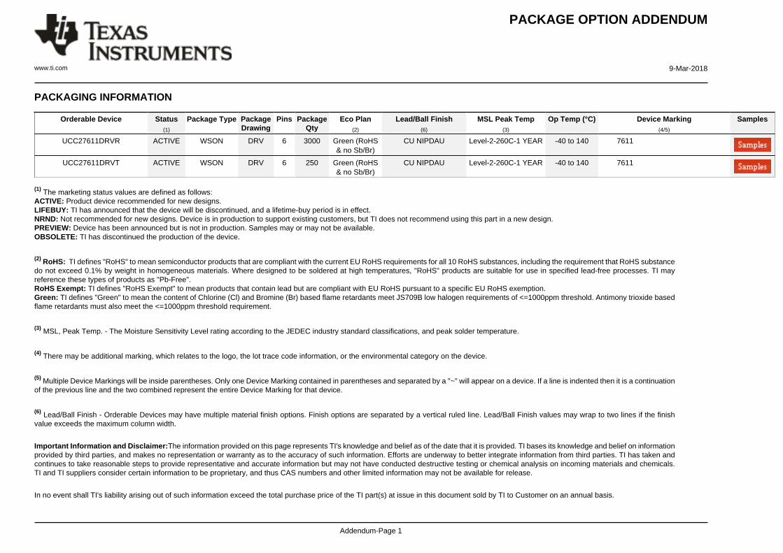
PACKAGING INFORMATION
Orderable Device Status(1)
Package Type PackageDrawing
Pins PackageQty
Eco Plan(2)
Lead/Ball Finish(6)
MSL Peak Temp(3)
Op Temp (°C) Device Marking(4/5)
Samples
UCC27611DRVR ACTIVE WSON DRV 6 3000 Green (RoHS& no Sb/Br)
CU NIPDAU Level-2-260C-1 YEAR -40 to 140 7611
UCC27611DRVT ACTIVE WSON DRV 6 250 Green (RoHS& no Sb/Br)
CU NIPDAU Level-2-260C-1 YEAR -40 to 140 7611
(1) The marketing status values are defined as follows:ACTIVE: Product device recommended for new designs.LIFEBUY: TI has announced that the device will be discontinued, and a lifetime-buy period is in effect.NRND: Not recommended for new designs. Device is in production to support existing customers, but TI does not recommend using this part in a new design.PREVIEW: Device has been announced but is not in production. Samples may or may not be available.OBSOLETE: TI has discontinued the production of the device.
(2) RoHS: TI defines "RoHS" to mean semiconductor products that are compliant with the current EU RoHS requirements for all 10 RoHS substances, including the requirement that RoHS substancedo not exceed 0.1% by weight in homogeneous materials. Where designed to be soldered at high temperatures, "RoHS" products are suitable for use in specified lead-free processes. TI mayreference these types of products as "Pb-Free".RoHS Exempt: TI defines "RoHS Exempt" to mean products that contain lead but are compliant with EU RoHS pursuant to a specific EU RoHS exemption.Green: TI defines "Green" to mean the content of Chlorine (Cl) and Bromine (Br) based flame retardants meet JS709B low halogen requirements of <=1000ppm threshold. Antimony trioxide basedflame retardants must also meet the <=1000ppm threshold requirement.
(3) MSL, Peak Temp. - The Moisture Sensitivity Level rating according to the JEDEC industry standard classifications, and peak solder temperature.
(4) There may be additional marking, which relates to the logo, the lot trace code information, or the environmental category on the device.
(5) Multiple Device Markings will be inside parentheses. Only one Device Marking contained in parentheses and separated by a "~" will appear on a device. If a line is indented then it is a continuationof the previous line and the two combined represent the entire Device Marking for that device.
(6) Lead/Ball Finish - Orderable Devices may have multiple material finish options. Finish options are separated by a vertical ruled line. Lead/Ball Finish values may wrap to two lines if the finishvalue exceeds the maximum column width.
Important Information and Disclaimer:The information provided on this page represents TI's knowledge and belief as of the date that it is provided. TI bases its knowledge and belief on informationprovided by third parties, and makes no representation or warranty as to the accuracy of such information. Efforts are underway to better integrate information from third parties. TI has taken andcontinues to take reasonable steps to provide representative and accurate information but may not have conducted destructive testing or chemical analysis on incoming materials and chemicals.TI and TI suppliers consider certain information to be proprietary, and thus CAS numbers and other limited information may not be available for release.
In no event shall TI's liability arising out of such information exceed the total purchase price of the TI part(s) at issue in this document sold by TI to Customer on an annual basis.
PACKAGE OPTION ADDENDUM
www.ti.com 9-Mar-2018
Addendum-Page 2
TAPE AND REEL INFORMATION
*All dimensions are nominal
Device PackageType
PackageDrawing
Pins SPQ ReelDiameter
(mm)
ReelWidth
W1 (mm)
A0(mm)
B0(mm)
K0(mm)
P1(mm)
W(mm)
Pin1Quadrant
UCC27611DRVR WSON DRV 6 3000 180.0 8.4 2.3 2.3 1.15 4.0 8.0 Q2
UCC27611DRVT WSON DRV 6 250 180.0 8.4 2.3 2.3 1.15 4.0 8.0 Q2
PACKAGE MATERIALS INFORMATION
www.ti.com 9-Mar-2018
Pack Materials-Page 1
*All dimensions are nominal
Device Package Type Package Drawing Pins SPQ Length (mm) Width (mm) Height (mm)
UCC27611DRVR WSON DRV 6 3000 210.0 185.0 35.0
UCC27611DRVT WSON DRV 6 250 210.0 185.0 35.0
PACKAGE MATERIALS INFORMATION
www.ti.com 9-Mar-2018
Pack Materials-Page 2
GENERIC PACKAGE VIEW
Images above are just a representation of the package family, actual package may vary.Refer to the product data sheet for package details.
DRV 6 WSON - 0.8 mm max heightPLASTIC SMALL OUTLINE - NO LEAD
4206925/F
www.ti.com
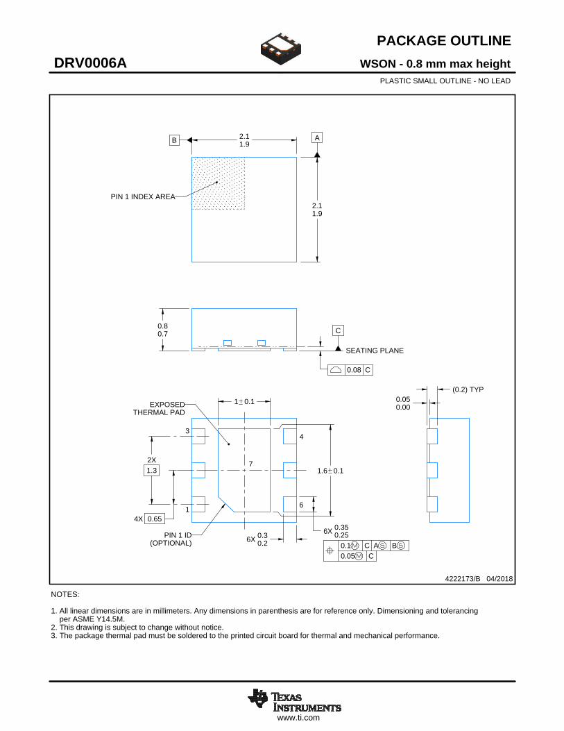
PACKAGE OUTLINE
C
6X 0.350.25
1.6 0.1
6X 0.30.2
2X1.3
1 0.1
4X 0.65
0.80.7
0.050.00
B 2.11.9
A
2.11.9
(0.2) TYP
WSON - 0.8 mm max heightDRV0006APLASTIC SMALL OUTLINE - NO LEAD
4222173/B 04/2018
PIN 1 INDEX AREA
SEATING PLANE
0.08 C
1
34
6
(OPTIONAL)PIN 1 ID
0.1 C A B0.05 C
THERMAL PADEXPOSED
7
NOTES: 1. All linear dimensions are in millimeters. Any dimensions in parenthesis are for reference only. Dimensioning and tolerancing per ASME Y14.5M. 2. This drawing is subject to change without notice. 3. The package thermal pad must be soldered to the printed circuit board for thermal and mechanical performance.
SCALE 5.500
www.ti.com
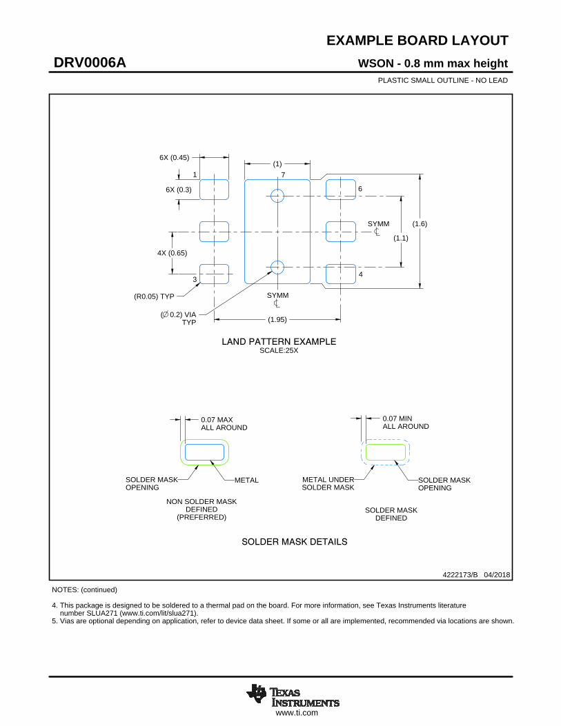
EXAMPLE BOARD LAYOUT
0.07 MINALL AROUND
0.07 MAXALL AROUND
(1)
4X (0.65)
(1.95)
6X (0.3)
6X (0.45)
(1.6)
(R0.05) TYP
( 0.2) VIATYP
(1.1)
WSON - 0.8 mm max heightDRV0006APLASTIC SMALL OUTLINE - NO LEAD
4222173/B 04/2018
SYMM
1
34
6
SYMM
LAND PATTERN EXAMPLESCALE:25X
7
NOTES: (continued) 4. This package is designed to be soldered to a thermal pad on the board. For more information, see Texas Instruments literature number SLUA271 (www.ti.com/lit/slua271).5. Vias are optional depending on application, refer to device data sheet. If some or all are implemented, recommended via locations are shown.
SOLDER MASKOPENINGSOLDER MASK
METAL UNDER
SOLDER MASKDEFINED
METALSOLDER MASKOPENING
SOLDER MASK DETAILS
NON SOLDER MASKDEFINED
(PREFERRED)
www.ti.com
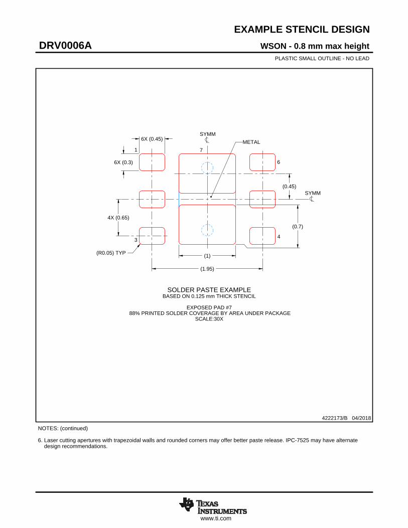
EXAMPLE STENCIL DESIGN
6X (0.3)
6X (0.45)
4X (0.65)
(0.7)
(1)
(1.95)
(R0.05) TYP
(0.45)
WSON - 0.8 mm max heightDRV0006APLASTIC SMALL OUTLINE - NO LEAD
4222173/B 04/2018
NOTES: (continued) 6. Laser cutting apertures with trapezoidal walls and rounded corners may offer better paste release. IPC-7525 may have alternate design recommendations.
SOLDER PASTE EXAMPLEBASED ON 0.125 mm THICK STENCIL
EXPOSED PAD #7
88% PRINTED SOLDER COVERAGE BY AREA UNDER PACKAGESCALE:30X
SYMM
1
3 4
6
SYMM
METAL7
IMPORTANT NOTICE
Texas Instruments Incorporated (TI) reserves the right to make corrections, enhancements, improvements and other changes to itssemiconductor products and services per JESD46, latest issue, and to discontinue any product or service per JESD48, latest issue. Buyersshould obtain the latest relevant information before placing orders and should verify that such information is current and complete.TI’s published terms of sale for semiconductor products (http://www.ti.com/sc/docs/stdterms.htm) apply to the sale of packaged integratedcircuit products that TI has qualified and released to market. Additional terms may apply to the use or sale of other types of TI products andservices.Reproduction of significant portions of TI information in TI data sheets is permissible only if reproduction is without alteration and isaccompanied by all associated warranties, conditions, limitations, and notices. TI is not responsible or liable for such reproduceddocumentation. Information of third parties may be subject to additional restrictions. Resale of TI products or services with statementsdifferent from or beyond the parameters stated by TI for that product or service voids all express and any implied warranties for theassociated TI product or service and is an unfair and deceptive business practice. TI is not responsible or liable for any such statements.Buyers and others who are developing systems that incorporate TI products (collectively, “Designers”) understand and agree that Designersremain responsible for using their independent analysis, evaluation and judgment in designing their applications and that Designers havefull and exclusive responsibility to assure the safety of Designers' applications and compliance of their applications (and of all TI productsused in or for Designers’ applications) with all applicable regulations, laws and other applicable requirements. Designer represents that, withrespect to their applications, Designer has all the necessary expertise to create and implement safeguards that (1) anticipate dangerousconsequences of failures, (2) monitor failures and their consequences, and (3) lessen the likelihood of failures that might cause harm andtake appropriate actions. Designer agrees that prior to using or distributing any applications that include TI products, Designer willthoroughly test such applications and the functionality of such TI products as used in such applications.TI’s provision of technical, application or other design advice, quality characterization, reliability data or other services or information,including, but not limited to, reference designs and materials relating to evaluation modules, (collectively, “TI Resources”) are intended toassist designers who are developing applications that incorporate TI products; by downloading, accessing or using TI Resources in anyway, Designer (individually or, if Designer is acting on behalf of a company, Designer’s company) agrees to use any particular TI Resourcesolely for this purpose and subject to the terms of this Notice.TI’s provision of TI Resources does not expand or otherwise alter TI’s applicable published warranties or warranty disclaimers for TIproducts, and no additional obligations or liabilities arise from TI providing such TI Resources. TI reserves the right to make corrections,enhancements, improvements and other changes to its TI Resources. TI has not conducted any testing other than that specificallydescribed in the published documentation for a particular TI Resource.Designer is authorized to use, copy and modify any individual TI Resource only in connection with the development of applications thatinclude the TI product(s) identified in such TI Resource. NO OTHER LICENSE, EXPRESS OR IMPLIED, BY ESTOPPEL OR OTHERWISETO ANY OTHER TI INTELLECTUAL PROPERTY RIGHT, AND NO LICENSE TO ANY TECHNOLOGY OR INTELLECTUAL PROPERTYRIGHT OF TI OR ANY THIRD PARTY IS GRANTED HEREIN, including but not limited to any patent right, copyright, mask work right, orother intellectual property right relating to any combination, machine, or process in which TI products or services are used. Informationregarding or referencing third-party products or services does not constitute a license to use such products or services, or a warranty orendorsement thereof. Use of TI Resources may require a license from a third party under the patents or other intellectual property of thethird party, or a license from TI under the patents or other intellectual property of TI.TI RESOURCES ARE PROVIDED “AS IS” AND WITH ALL FAULTS. TI DISCLAIMS ALL OTHER WARRANTIES ORREPRESENTATIONS, EXPRESS OR IMPLIED, REGARDING RESOURCES OR USE THEREOF, INCLUDING BUT NOT LIMITED TOACCURACY OR COMPLETENESS, TITLE, ANY EPIDEMIC FAILURE WARRANTY AND ANY IMPLIED WARRANTIES OFMERCHANTABILITY, FITNESS FOR A PARTICULAR PURPOSE, AND NON-INFRINGEMENT OF ANY THIRD PARTY INTELLECTUALPROPERTY RIGHTS. TI SHALL NOT BE LIABLE FOR AND SHALL NOT DEFEND OR INDEMNIFY DESIGNER AGAINST ANY CLAIM,INCLUDING BUT NOT LIMITED TO ANY INFRINGEMENT CLAIM THAT RELATES TO OR IS BASED ON ANY COMBINATION OFPRODUCTS EVEN IF DESCRIBED IN TI RESOURCES OR OTHERWISE. IN NO EVENT SHALL TI BE LIABLE FOR ANY ACTUAL,DIRECT, SPECIAL, COLLATERAL, INDIRECT, PUNITIVE, INCIDENTAL, CONSEQUENTIAL OR EXEMPLARY DAMAGES INCONNECTION WITH OR ARISING OUT OF TI RESOURCES OR USE THEREOF, AND REGARDLESS OF WHETHER TI HAS BEENADVISED OF THE POSSIBILITY OF SUCH DAMAGES.Unless TI has explicitly designated an individual product as meeting the requirements of a particular industry standard (e.g., ISO/TS 16949and ISO 26262), TI is not responsible for any failure to meet such industry standard requirements.Where TI specifically promotes products as facilitating functional safety or as compliant with industry functional safety standards, suchproducts are intended to help enable customers to design and create their own applications that meet applicable functional safety standardsand requirements. Using products in an application does not by itself establish any safety features in the application. Designers mustensure compliance with safety-related requirements and standards applicable to their applications. Designer may not use any TI products inlife-critical medical equipment unless authorized officers of the parties have executed a special contract specifically governing such use.Life-critical medical equipment is medical equipment where failure of such equipment would cause serious bodily injury or death (e.g., lifesupport, pacemakers, defibrillators, heart pumps, neurostimulators, and implantables). Such equipment includes, without limitation, allmedical devices identified by the U.S. Food and Drug Administration as Class III devices and equivalent classifications outside the U.S.TI may expressly designate certain products as completing a particular qualification (e.g., Q100, Military Grade, or Enhanced Product).Designers agree that it has the necessary expertise to select the product with the appropriate qualification designation for their applicationsand that proper product selection is at Designers’ own risk. Designers are solely responsible for compliance with all legal and regulatoryrequirements in connection with such selection.Designer will fully indemnify TI and its representatives against any damages, costs, losses, and/or liabilities arising out of Designer’s non-compliance with the terms and provisions of this Notice.
Mailing Address: Texas Instruments, Post Office Box 655303, Dallas, Texas 75265Copyright © 2018, Texas Instruments Incorporated