Embed Size (px)
Citation preview
1
E-BeamLithography
Ivor Brodie and Julius Muray”The Physics of Micro/Nano-Fabrication”
2
• Spot size <100 Å as compared to photolithography (5000 Å).• High speed and precision of e-beam deflection and modulation.• Good control over the energy and dose delivered to resist.
E-Beam Lithography:Some Pros and Cons
• Either scanning the beam by controlling its deflection from a computer (sequential exposure) or electron imaging through a special mask (parallel exposure).• Exposure in the spot takes ~10-7 s, but there are ~1010 spots that are typically required → high speed is important.• 1010 spots requires also a precision of ~1ppm along each of the axis → strict demands on DA converters, max areas of up to 1 mm2 can be exposed by direct beam deflection.• Also, a mechanical table is used to move the beam along larger distances.
(Then, alignment is made for each table position, either by checking for registration marks, or use laser interferometers to precisely measure the table movement.)
2
3
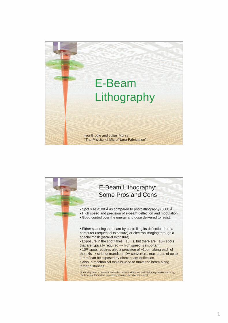
Types of E-Beam MachinesScanning systems
Single beamsystem
Multiple beamsystem
Vector Raster Vector Raster
Hybrid systems
Shaped beam Character projection
Parallel exposuresystems
Photocathodeprojection
e-Imageprojection
Fly’s eye lensprojection
• pattern information is stored in masks• high throughput• less expensive
• pattern information in computer’s memory• distortion-, and proximity corrections are needed• expensive but flexible
Two distinct uses of e-beam lithography:1. direct exposure of resist for device fabrication2. mask fabrication for subsequent optical lithography
4
Raster- vs Vector Control
• The raster-scan systems meticulously cover the area of pattern, switching the e-beam on and off as required by the patterns shape
• The vector-control systems deflect the beam to follow paths dictated by the pattern. “Go to that address and do exposure there”.
Analogy:
Compare the bitmap- and vector formats for digital-image files ( i.e. “*.bmp” vs “*.eps”)
3
5
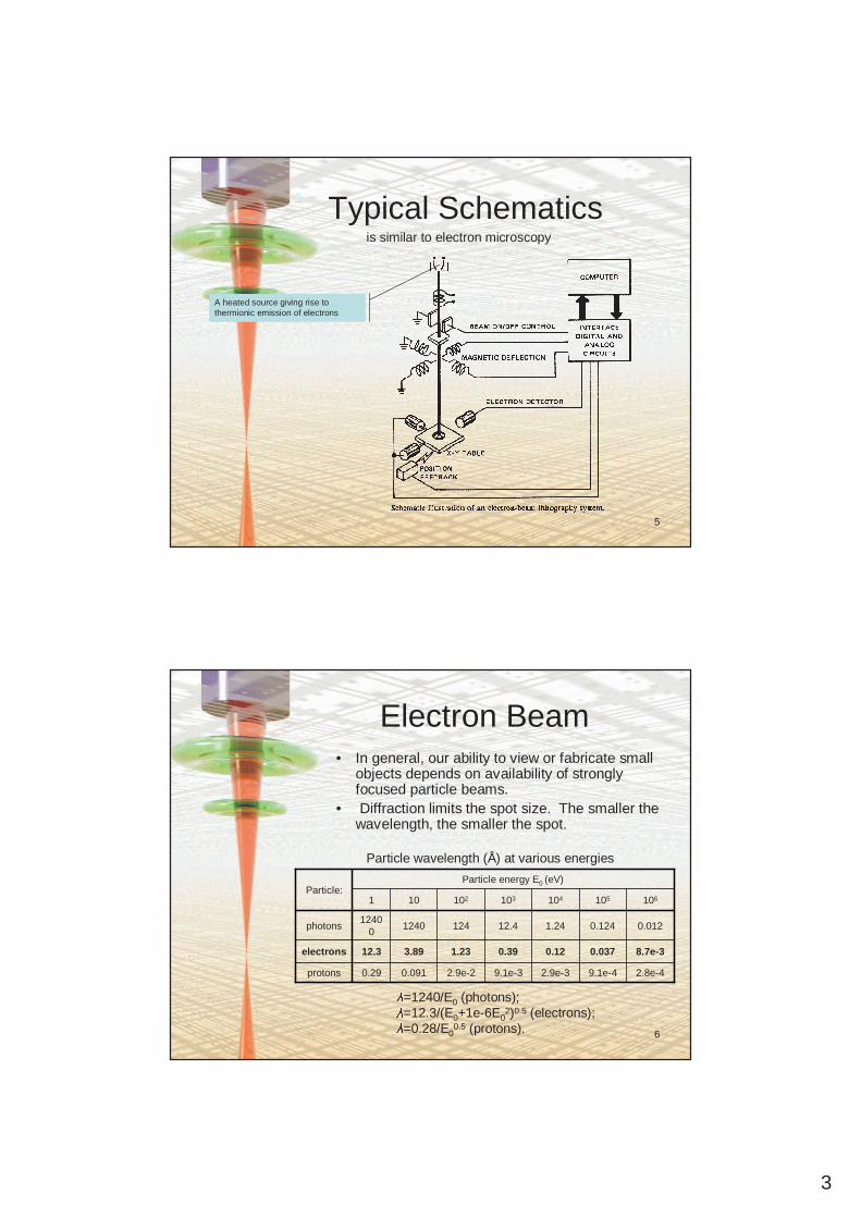
Typical Schematics
A heated source giving rise to thermionic emission of electrons
is similar to electron microscopy
6
Electron Beam• In general, our ability to view or fabricate small
objects depends on availability of strongly focused particle beams.
• Diffraction limits the spot size. The smaller the wavelength, the smaller the spot.
Particle energy E0 (eV)Particle:
2.9e-3
0.12
1.24
104
9.1e-4
0.037
0.124
105
2.8e-4
8.7e-3
0.012
106
9.1e-32.9e-20.0910.29protons
0.391.233.8912.3electrons
12.412412401240
0photons
103102101 λ=1240/E0 (photons); λ=12.3/(E0+1e-6E0
2)0.5 (electrons); λ=0.28/E0
0.5 (protons).
Particle wavelength (Å) at various energies
4
7
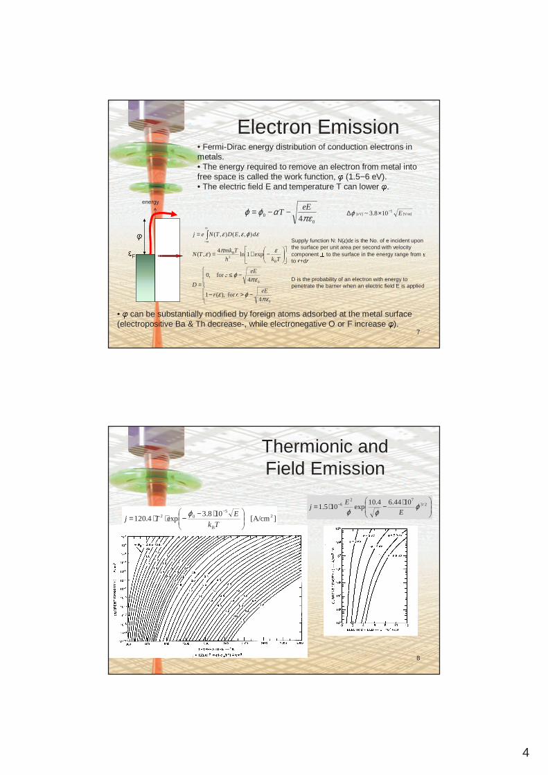
Electron Emission• Fermi-Dirac energy distribution of conduction electrons in metals.• The energy required to remove an electron from metal into free space is called the work function, φ (1.5−6 eV).• The electric field E and temperature T can lower φ .
00 4 επ
αϕϕ eET −−= [V/m]
5[eV] 108.3~ E−×∆ϕ
• φ can be substantially modified by foreign atoms adsorbed at the metal surface (electropositive Ba & Th decrease-, while electronegative O or F increase φ ).
energyεF
φ
−>−
−≤=
−+=
= ∫∞
∞−
0
0
B3
B
4for ),(1
4for ,0
exp1ln4
),(
),,(),(
επϕε
επϕ
επε
εϕεε
eEεr
eEεD
Tkh
TkmTN
dEDTNejSupply function N: N(ε )dε is the No. of e incident upon the surface per unit area per second with velocity component ┴ to the surface in the energy range from εto ε +dεD is the probability of an electron with energy to penetrate the barrier when an electric field E is applied
8
Thermionic and Field Emission
⋅−⋅= − 2/372
6 1044.64.10exp105.1 ϕ
ϕϕ E
Ej
][A/cm108.3
exp4.120 2
B
502
⋅−−⋅⋅=−
Tk
ETj
ϕ

5
9
Cathodes
Cathode Requirements
• The uniformity of emission over the cathode surface• The current density required from the cathode• The energy distribution of the emitted electrons• The current fluctuations as a function of time• The evaporation of material from the cathode surface• The ability of the cathode to operate in a given environment• The lifetime of the cathode under given operating conditions
10
Practical Cathodes• Thermionic cathodes:thoriated tungsten (1700◦ C & 3 A/cm2); WC+ThO2
→ W + Th + CO2 (→ bad vacuum)
lanthanum hexaborid;oxide coated (750 C & 0.5 A/cm2); Ni coated by Sr-O, Ba-O, Ca-O; can be poisoned
tungsten sponge filled with Ba/Ca aluminate (1100 C & 5 A/cm2)
• Field-Emission cathodes (best but most expensive):- emission occurs in ”lobes” because of crystal facets present at the surface- emission can be unstable.
6
11
e-Beam Characteristics
Assumptions: • e-beams are circular;• emitted e have Maxwell velocity distribution, both axially and radially;• object and image are related by the Helmholtz-Lagrange relation;• space-charge forces are neglected.
The brightness is the e-currentper unit solid angle
kT
eVj
πβ =max
j is the current density at the cathode;V is the acceleration energy;T is the cathode temperature.
12
E-Guns: Self-bias
http://jan.ucc.nau.edu/~wittke/Microprobe/Column-ElectronGun.html
A bias resistor allows the gun to be self-regulating. Any increase of the emission current causes a larger voltage drop across the bias resistor and a larger negative voltage is applied to the Wehnelt, reducing the current. As the emission increases, so does the voltage difference between Wehnelt and filament, causing the emission to saturate. Proper bias voltage also optimizes the electron beam brightness.
7
13
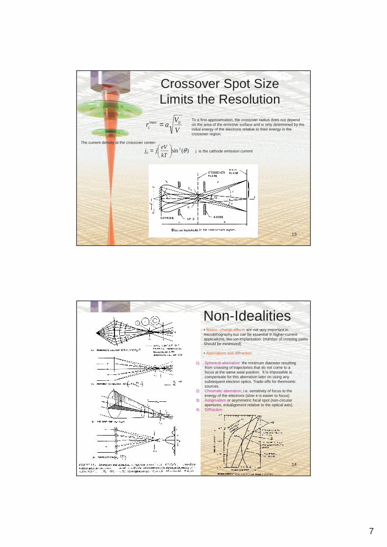
Crossover Spot SizeLimits the Resolution
V
Varc
0max =
)(sin20 θ
=kT
eVjj
To a first approximation, the crossover radius does not depend on the area of the emissive surface and is only determined by the initial energy of the electrons relative to their energy in the crossover region.
The current density at the crossover center:
j is the cathode emission current
14
Non-Idealities• Space –charge effects are not very important in microlithography but can be essential in higher-current applications, like ion-implantation. (number of crossing pathsShould be minimized)
• Aberrations and diffraction
1) Spherical aberration: the minimum diameter resulting from crossing of trajectories that do not come to a focus at the same axial position. It is impossible to compensate for this aberration later on using any subsequent electron optics. Trade-offs for thermionic sources.
2) Chromatic aberration, i.e. sensitivity of focus to the energy of the electrons (slow e is easier to focus)
3) Astigmatism or asymmetric focal spot (non-circular apertures, misalignment relative to the optical axis).
4) Diffraction
8
15
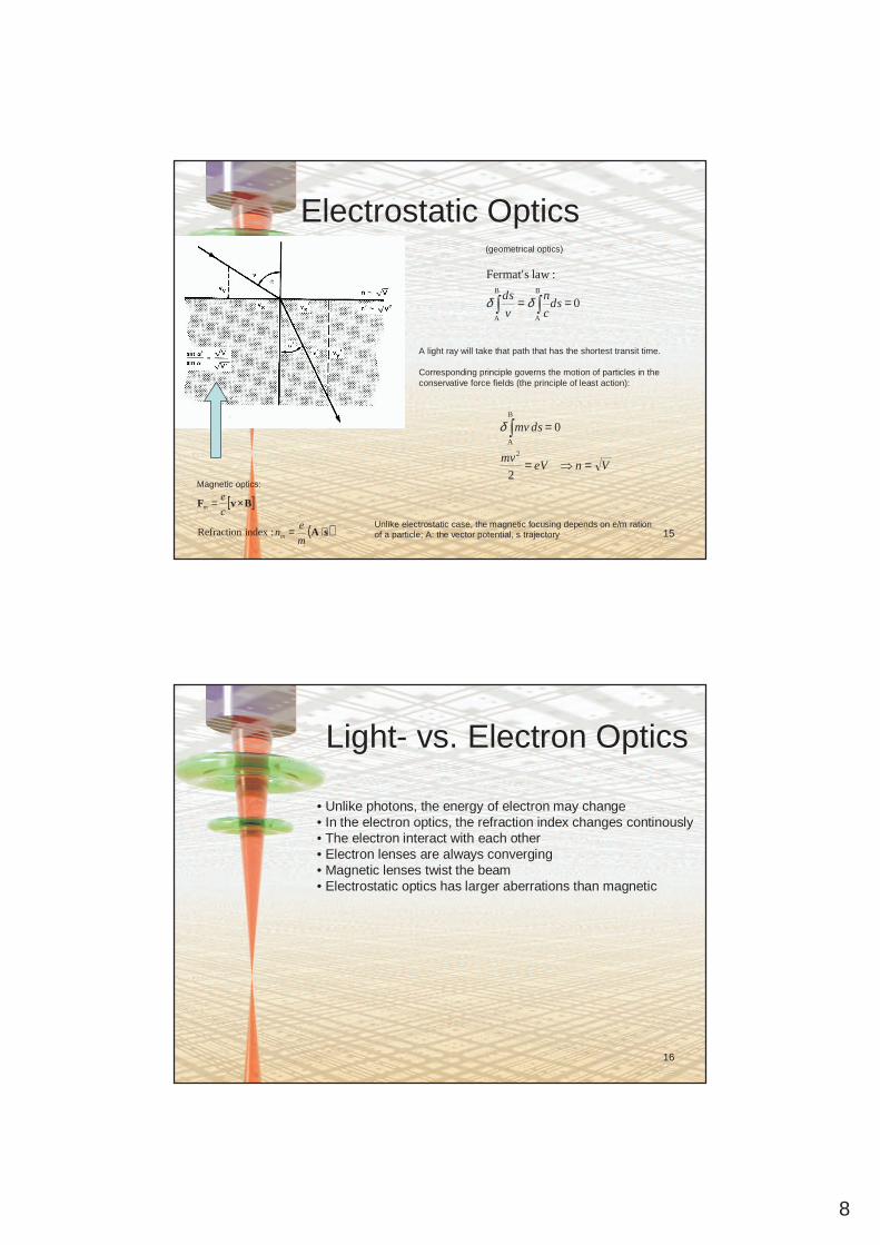
Electrostatic Optics
dsc
n
v
ds∫∫ =B
A
B
A
:law sFermat'
δδ
0
:law sFermat'B
A
B
A
== ∫∫ dsc
n
v
ds δδ
VneVmv
dsmv
=⇒=
=∫
2
0
2
B
A
δ
(geometrical optics)
A light ray will take that path that has the shortest transit time.
Corresponding principle governs the motion of particles in the conservative force fields (the principle of least action):
[ ]
( )sA
BvF
⋅=
×=
m
en
c
e
m
m
:index RefractionUnlike electrostatic case, the magnetic focusing depends on e/m ration of a particle; A: the vector potential, s trajectory
Magnetic optics:
16
Light- vs. Electron Optics
• Unlike photons, the energy of electron may change• In the electron optics, the refraction index changes continously• The electron interact with each other• Electron lenses are always converging• Magnetic lenses twist the beam • Electrostatic optics has larger aberrations than magnetic
9
17
Electron Optics
1) Axially symmetric lenses where trajectories are || to fieldLongitudinal systems : focusing by small perp. Component2) Transverse systems (field perp. to the beam) more effective
dzBV
me
f ∫=2
1
208
/1
2
1
12
1631
−=V
VV
df
2
1
12
8
31
−=V
VV
df
18
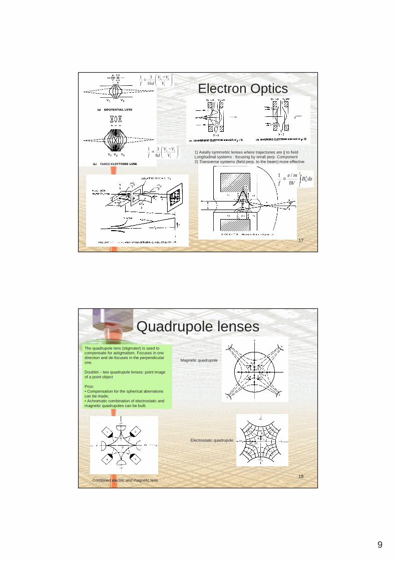
Quadrupole lenses
Magnetic quadrupole
Electrostatic quadrupole
The quadrupole lens (stigmator) is used to compensate for astigmatism. Focuses in one direction and de-focuses in the perpendicular one.
Doublet – two quadrupole lenses: point image of a point object
Pros:• Compensation for the spherical aberrations can be made;• Achromatic combination of electrostatic and magnetic quadrupoles can be built.
Combined electric and magnetic lens
10
19
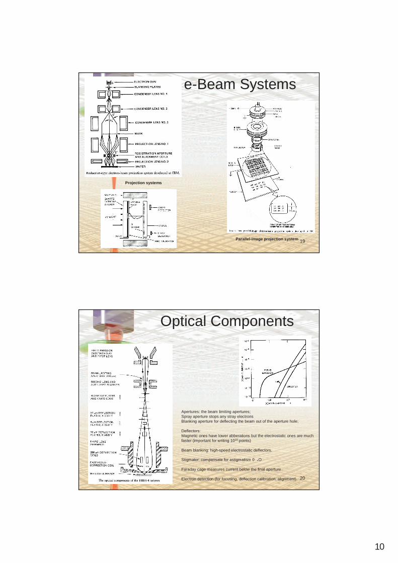
e-Beam Systems
Projection systems
Parallel-image projection system
20
Optical Components
Apertures: the beam limiting apertures;Spray aperture stops any stray electronsBlanking aperture for deflecting the beam out of the aperture hole;
Deflectors:Magnetic ones have lower abberations but the electrostatic ones are much faster (important for writing 1010 points)
Beam blanking: high-speed electrostatic deflectors.
Stigmator: compensate for astigmatism 0→ O
Faraday cage measures current below the final aperture
Electron detection (for focusing, deflection calibration, alignment).
11
21
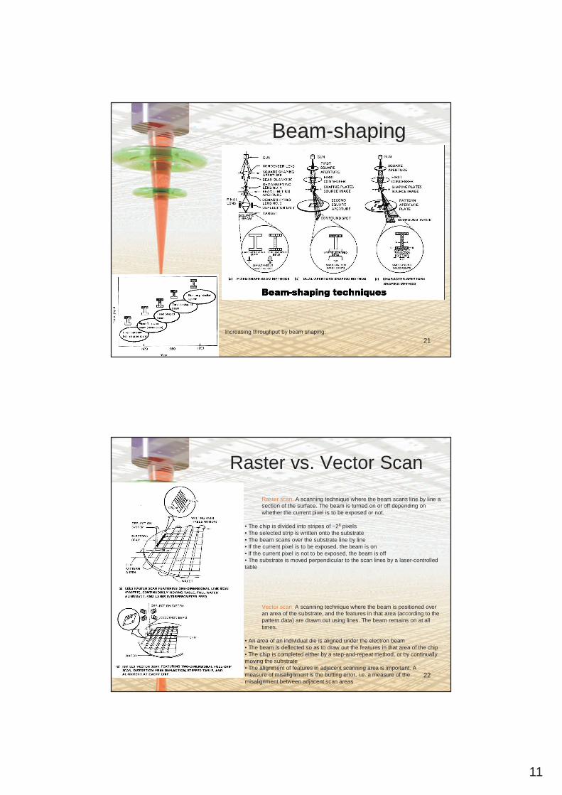
Beam-shaping
Increasing throughput by beam shaping:
22
Raster vs. Vector Scan
Raster scan. A scanning technique where the beam scans line by line a section of the surface. The beam is turned on or off depending on whether the current pixel is to be exposed or not.
• The chip is divided into stripes of ~28 pixels • The selected strip is written onto the substrate • The beam scans over the substrate line by line • If the current pixel is to be exposed, the beam is on • If the current pixel is not to be exposed, the beam is off • The substrate is moved perpendicular to the scan lines by a laser-controlled table
Vector scan. A scanning technique where the beam is positioned over an area of the substrate, and the features in that area (according to the pattern data) are drawn out using lines. The beam remains on at all times.
• An area of an individual die is aligned under the electron beam• The beam is deflected so as to draw out the features in that area of the chip • The chip is completed either by a step-and-repeat method, or by continually moving the substrate • The alignment of features in adjacent scanning area is important. A measure of misalignment is the butting error, i.e. a measure of the misalignment between adjacent scan areas
12
23
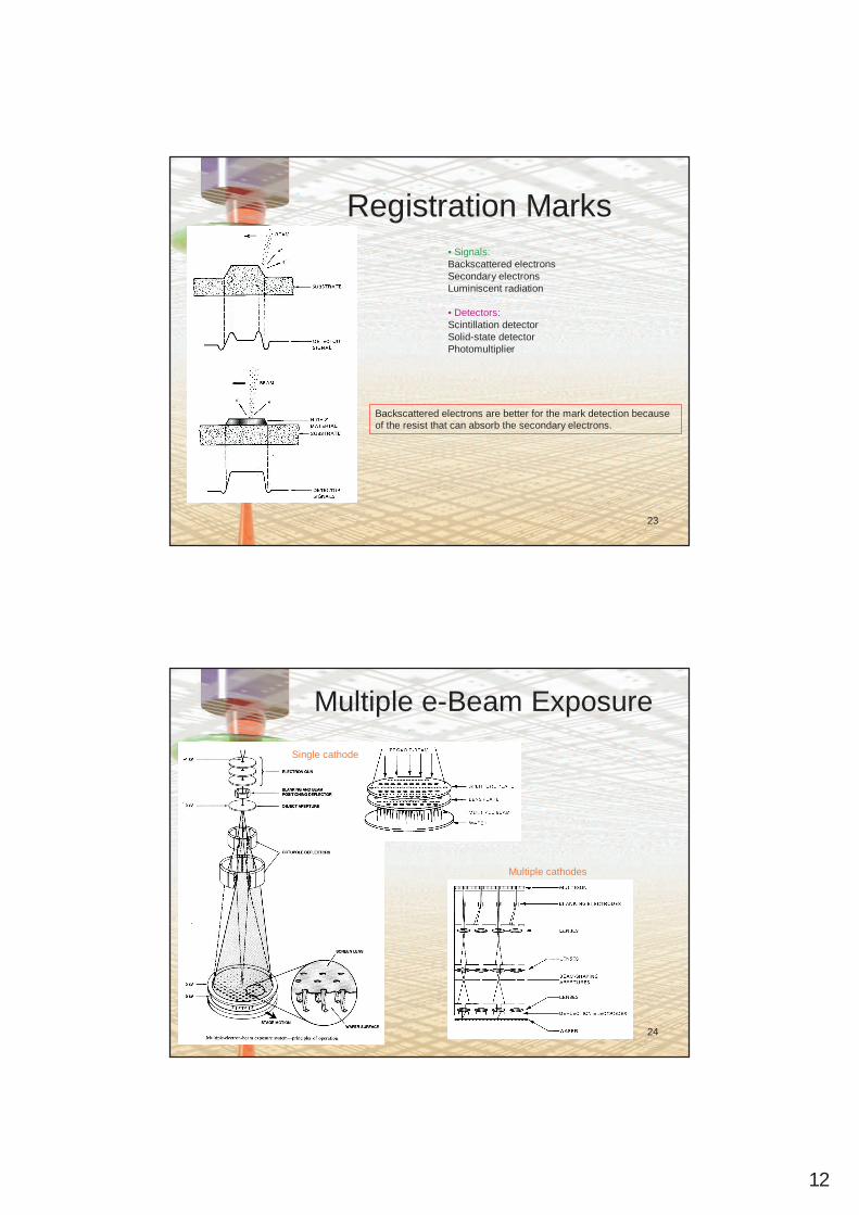
Registration Marks• Signals:Backscattered electronsSecondary electronsLuminiscent radiation
• Detectors:Scintillation detectorSolid-state detectorPhotomultiplier
Backscattered electrons are better for the mark detection because of the resist that can absorb the secondary electrons.
24
Multiple e-Beam Exposure
Single cathode
Multiple cathodes
13
25
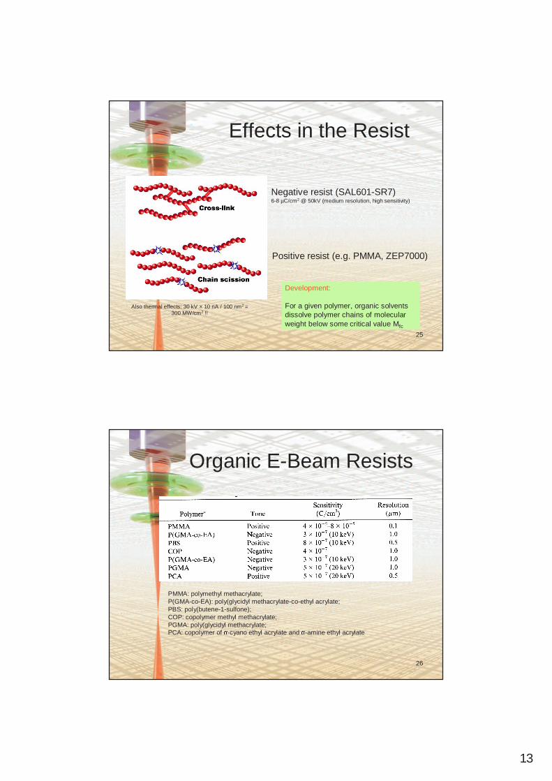
Effects in the Resist
Negative resist (SAL601-SR7)6-8 µC/cm2 @ 50kV (medium resolution, high sensitivity)
Positive resist (e.g. PMMA, ZEP7000)
Also thermal effects: 30 kV × 10 nA / 100 nm2 = 300 MW/cm2 !!
Development:
For a given polymer, organic solvents dissolve polymer chains of molecular weight below some critical value Mfc
26
Organic E-Beam Resists
PMMA: polymethyl methacrylate;P(GMA-co-EA): poly(glycidyl methacrylate-co-ethyl acrylate;PBS: poly(butene-1-sulfone);COP: copolymer methyl methacrylate;PGMA: poly(glycidyl methacrylate;PCA: copolymer of α -cyano ethyl acrylate and α -amine ethyl acrylate
14
27
High-Res. Positive Inorganic Resists
Self-development of metal halides by e-beam
28
Sensitivity
Contrast γ =|log(D0/Dm|-1 (negative resists)
D0 is the dose required to polymerize 100% of thickness;Dm is the minimum dose required for any detectable polymerized layer to form
15
29
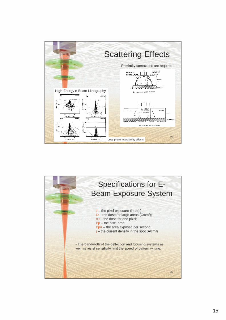
Scattering EffectsProximity corrections are required
High-Energy e-Beam Lithography
Less prone to proximity effects
30
Specifications for E-Beam Exposure Systemτ – the pixel exposure time (s);
D – the dose for large areas (C/cm2);fD – the dose for one pixel;l2p – the pixel area;l2p/τ – the area exposed per second;j – the current density in the spot (A/cm2)
• The bandwidth of the deflection and focusing systems as well as resist sensitivity limit the speed of pattern writing: