Embed Size (px)
Citation preview
1. Product profile
1.1 General description
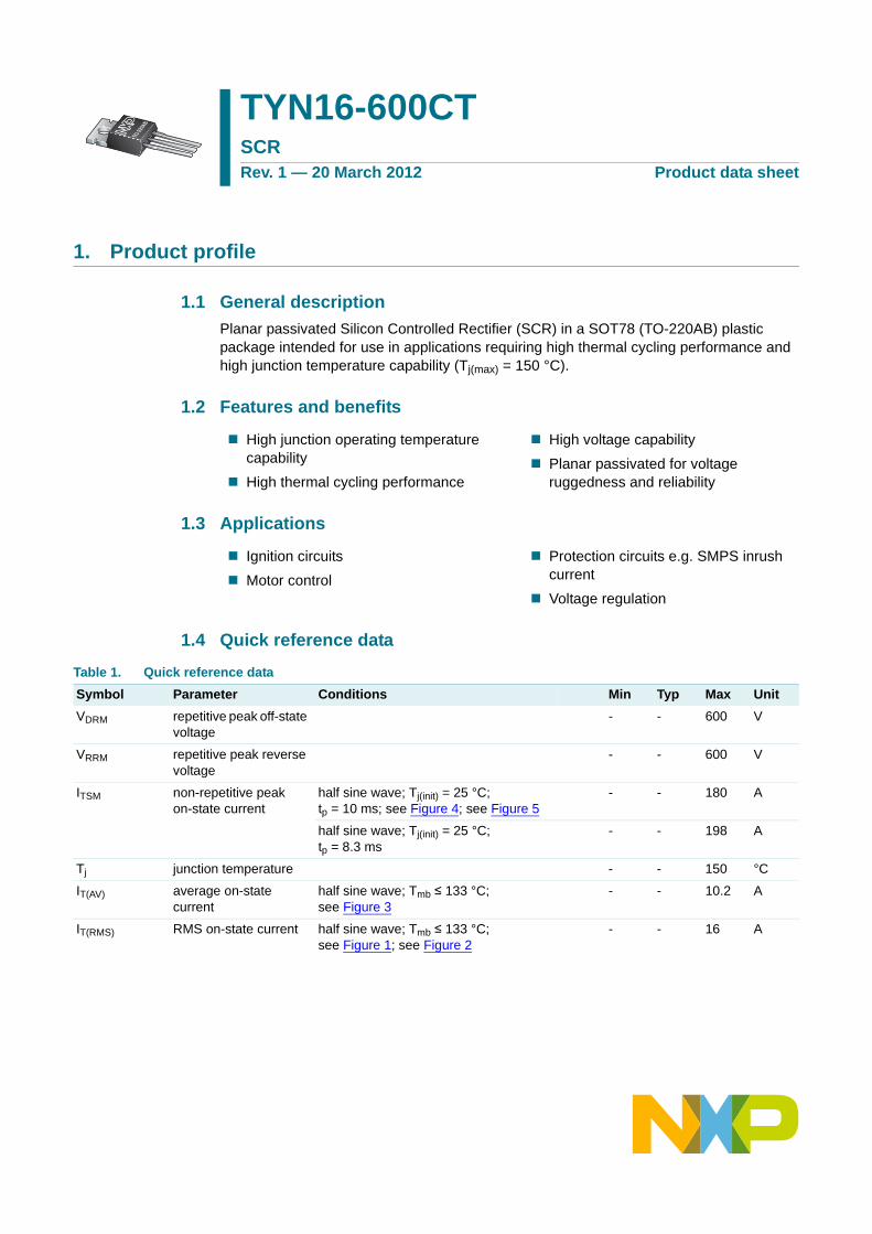
Planar passivated Silicon Controlled Rectifier (SCR) in a SOT78 (TO-220AB) plastic package intended for use in applications requiring high thermal cycling performance and high junction temperature capability (Tj(max) = 150 °C).
1.2 Features and benefits
High junction operating temperature capability
High thermal cycling performance
High voltage capability
Planar passivated for voltage ruggedness and reliability
1.3 Applications
Ignition circuits
Motor control
Protection circuits e.g. SMPS inrush current
Voltage regulation
1.4 Quick reference data
TYN16-600CTSCRRev. 1 — 20 March 2012 Product data sheet
TO-22
0AB
Table 1. Quick reference data
Symbol Parameter Conditions Min Typ Max Unit
VDRM repetitive peak off-state voltage
- - 600 V
VRRM repetitive peak reverse voltage
- - 600 V
ITSM non-repetitive peak on-state current
half sine wave; Tj(init) = 25 °C; tp = 10 ms; see Figure 4; see Figure 5
- - 180 A
half sine wave; Tj(init) = 25 °C; tp = 8.3 ms
- - 198 A
Tj junction temperature - - 150 °C
IT(AV) average on-state current
half sine wave; Tmb ≤ 133 °C;see Figure 3
- - 10.2 A
IT(RMS) RMS on-state current half sine wave; Tmb ≤ 133 °C;see Figure 1; see Figure 2
- - 16 A
NXP Semiconductors TYN16-600CTSCR
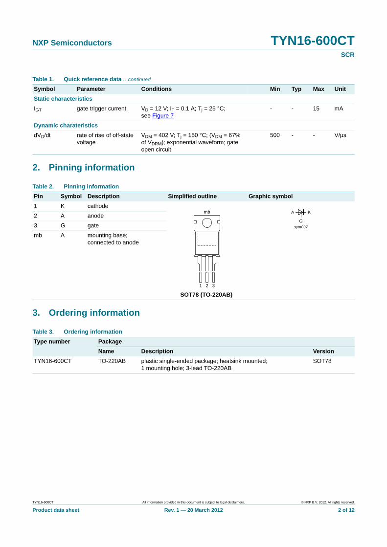
2. Pinning information
3. Ordering information
Static characteristics
IGT gate trigger current VD = 12 V; IT = 0.1 A; Tj = 25 °C;see Figure 7
- - 15 mA
Dynamic charateristics
dVD/dt rate of rise of off-state voltage
VDM = 402 V; Tj = 150 °C; (VDM = 67% of VDRM); exponential waveform; gate open circuit
500 - - V/µs
Table 1. Quick reference data …continued
Symbol Parameter Conditions Min Typ Max Unit
Table 2. Pinning information
Pin Symbol Description Simplified outline Graphic symbol
1 K cathode
SOT78 (TO-220AB)
2 A anode
3 G gate
mb A mounting base; connected to anode
1 2
mb
3
sym037
A K
G
Table 3. Ordering information
Type number Package
Name Description Version
TYN16-600CT TO-220AB plastic single-ended package; heatsink mounted; 1 mounting hole; 3-lead TO-220AB
SOT78
TYN16-600CT All information provided in this document is subject to legal disclaimers. © NXP B.V. 2012. All rights reserved.
Product data sheet Rev. 1 — 20 March 2012 2 of 12
NXP Semiconductors TYN16-600CTSCR
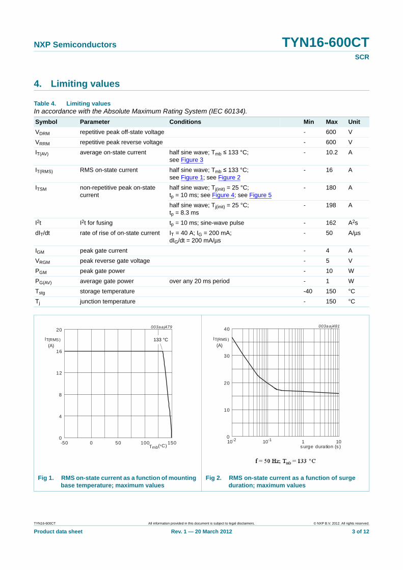
4. Limiting values
Table 4. Limiting valuesIn accordance with the Absolute Maximum Rating System (IEC 60134).
Symbol Parameter Conditions Min Max Unit
VDRM repetitive peak off-state voltage - 600 V
VRRM repetitive peak reverse voltage - 600 V
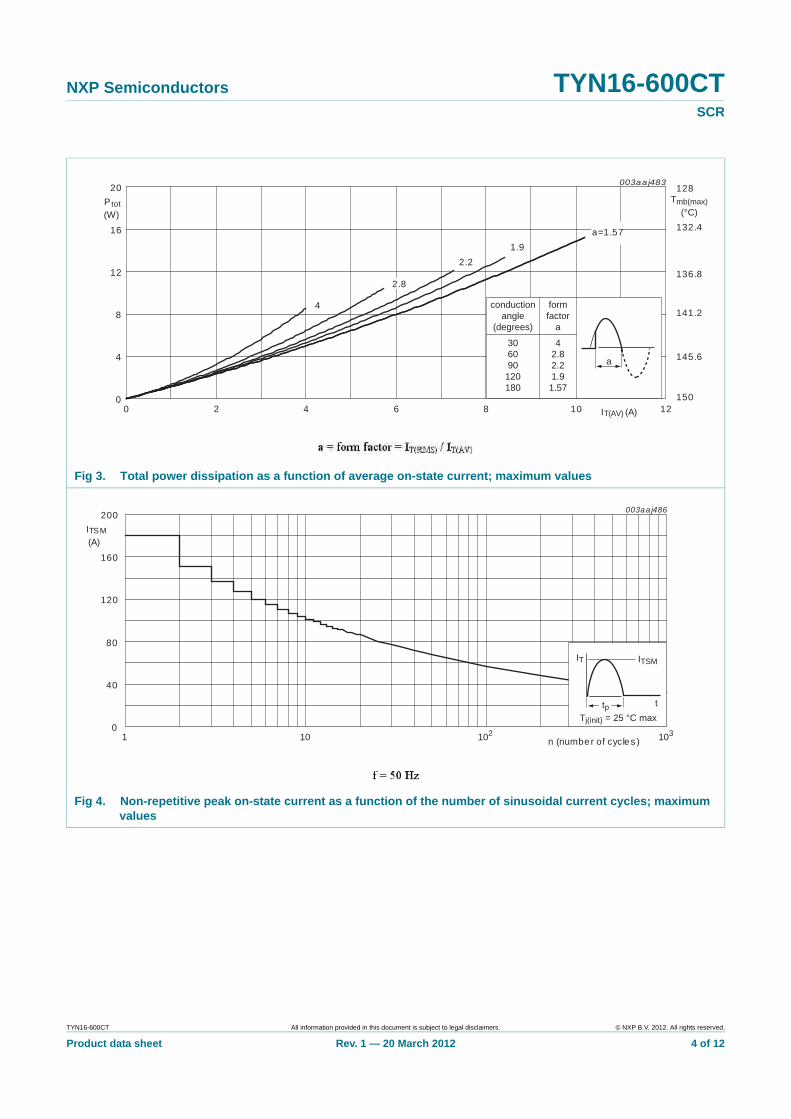
IT(AV) average on-state current half sine wave; Tmb ≤ 133 °C;see Figure 3
- 10.2 A
IT(RMS) RMS on-state current half sine wave; Tmb ≤ 133 °C;see Figure 1; see Figure 2
- 16 A
ITSM non-repetitive peak on-state current
half sine wave; Tj(init) = 25 °C; tp = 10 ms; see Figure 4; see Figure 5
- 180 A
half sine wave; Tj(init) = 25 °C; tp = 8.3 ms
- 198 A
I2t I2t for fusing tp = 10 ms; sine-wave pulse - 162 A2s
dIT/dt rate of rise of on-state current IT = 40 A; IG = 200 mA; dIG/dt = 200 mA/µs
- 50 A/µs
IGM peak gate current - 4 A
VRGM peak reverse gate voltage - 5 V
PGM peak gate power - 10 W
PG(AV) average gate power over any 20 ms period - 1 W
Tstg storage temperature -40 150 °C
Tj junction temperature - 150 °C
Fig 1. RMS on-state current as a function of mounting base temperature; maximum values
Fig 2. RMS on-state current as a function of surge duration; maximum values
003aa j479
0
4
8
12
16
20
-50 0 50 100 150Tmb (°C)
IT(RMS)(A)
133 °C
003aa j481
0
10
20
30
40
10-2 10-1 1 10surge duration (s )
IT(RMS)(A)
TYN16-600CT All information provided in this document is subject to legal disclaimers. © NXP B.V. 2012. All rights reserved.
Product data sheet Rev. 1 — 20 March 2012 3 of 12
NXP Semiconductors TYN16-600CTSCR
Fig 3. Total power dissipation as a function of average on-state current; maximum values
Fig 4. Non-repetitive peak on-state current as a function of the number of sinusoidal current cycles; maximum values
003aa j483
0
4
8
12
16
20
0 2 4 6 8 10 12IT(AV) (A)
Ptot(W)
a=1.571.9
2.2
2.8
4
150
141.2
136.8
128Tmb(max)
(°C)
145.6
132.4
conductionangle
(degrees)
formfactor
a
306090120180
42.82.21.91.57
a
003aa j486
0
40
80
120
160
200
1 10 102 103n (number of cycles )
ITSM(A)
tpTj(init) = 25 °C max
IT ITSM
t
TYN16-600CT All information provided in this document is subject to legal disclaimers. © NXP B.V. 2012. All rights reserved.
Product data sheet Rev. 1 — 20 March 2012 4 of 12
NXP Semiconductors TYN16-600CTSCR
5. Thermal characteristics
Fig 5. Non-repetitive peak on-state current as a function of pulse width for sinusoidal currents; maximum values
003aa j485
10
102
103
10-5 10-4 10-3 10-2tp (s )
ITSM(A)
tpTj(init) = 25 °C max
IT ITSM
t
(1)
Table 5. Thermal characteristics
Symbol Parameter Conditions Min Typ Max Unit
Rth(j-mb) thermal resistance from junction to mounting base
see Figure 6 - - 1.1 K/W
Rth(j-a) thermal resistance from junction to ambient
in free air - 60 - K/W
Fig 6. Transient thermal impedance from junction to mounting base as a function of pulse width
10-1
10-2
1
10
Zth(j-mb)(K/W)
10-3
tp (s)10-5 1 1010-110-210-4 10-3
tp
tp
T
P
t
Td =
003aaj448
TYN16-600CT All information provided in this document is subject to legal disclaimers. © NXP B.V. 2012. All rights reserved.
Product data sheet Rev. 1 — 20 March 2012 5 of 12
NXP Semiconductors TYN16-600CTSCR
6. Characteristics
Table 6. Characteristics
Symbol Parameter Conditions Min Typ Max Unit
Static characteristics
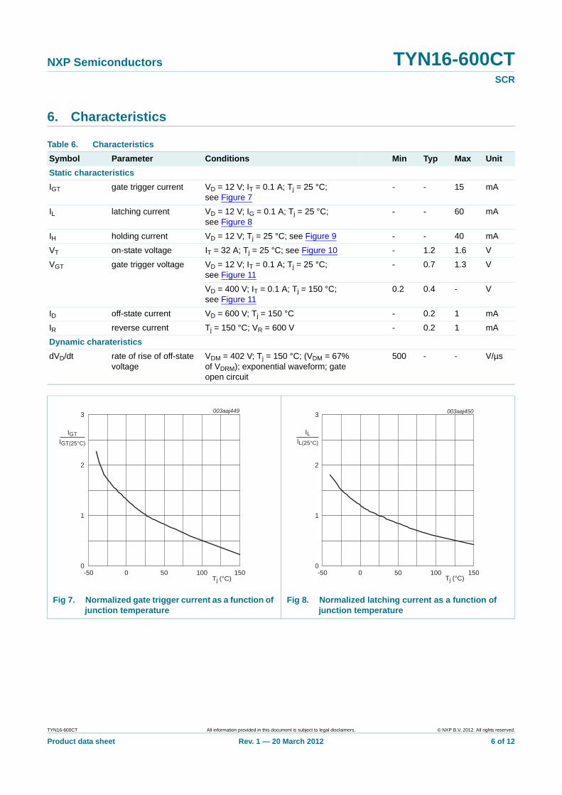
IGT gate trigger current VD = 12 V; IT = 0.1 A; Tj = 25 °C;see Figure 7
- - 15 mA
IL latching current VD = 12 V; IG = 0.1 A; Tj = 25 °C;see Figure 8
- - 60 mA
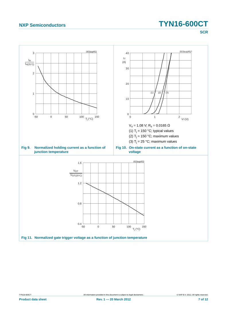
IH holding current VD = 12 V; Tj = 25 °C; see Figure 9 - - 40 mA
VT on-state voltage IT = 32 A; Tj = 25 °C; see Figure 10 - 1.2 1.6 V
VGT gate trigger voltage VD = 12 V; IT = 0.1 A; Tj = 25 °C;see Figure 11
- 0.7 1.3 V
VD = 400 V; IT = 0.1 A; Tj = 150 °C;see Figure 11
0.2 0.4 - V
ID off-state current VD = 600 V; Tj = 150 °C - 0.2 1 mA
IR reverse current Tj = 150 °C; VR = 600 V - 0.2 1 mA
Dynamic charateristics
dVD/dt rate of rise of off-state voltage
VDM = 402 V; Tj = 150 °C; (VDM = 67% of VDRM); exponential waveform; gate open circuit
500 - - V/µs
Fig 7. Normalized gate trigger current as a function of junction temperature
Fig 8. Normalized latching current as a function of junction temperature
Tj (°C)-50 1501000 50
003aaj449
1
2
3
0
IGTIGT(25°C)
Tj (°C)-50 1501000 50
003aaj450
1
2
3
0
ILIL(25°C)
TYN16-600CT All information provided in this document is subject to legal disclaimers. © NXP B.V. 2012. All rights reserved.
Product data sheet Rev. 1 — 20 March 2012 6 of 12
NXP Semiconductors TYN16-600CTSCR
Vo = 1.08 V; Rs = 0.0165 Ω
(1) Tj = 150 °C; typical values
(2) Tj = 150 °C; maximum values
(3) Tj = 25 °C; maximum values
Fig 9. Normalized holding current as a function of junction temperature
Fig 10. On-state current as a function of on-state voltage
Fig 11. Normalized gate trigger voltage as a function of junction temperature
Tj (°C)-50 1501000 50
003aaj451
1
2
3
IHIH(25°C)
0
003aa j452
0
10
20
30
40
0 1 2VT (V)
IT (A)
(1) (2) (3)
Tj (°C)-50 1501000 50
003aaj453
0.8
1.2
1.6
0.4
VGT VGT(25°C)
TYN16-600CT All information provided in this document is subject to legal disclaimers. © NXP B.V. 2012. All rights reserved.
Product data sheet Rev. 1 — 20 March 2012 7 of 12
NXP Semiconductors TYN16-600CTSCR
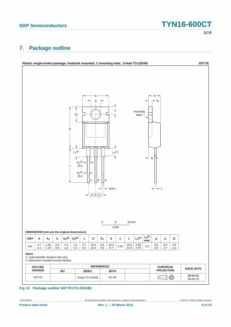
7. Package outline
Fig 12. Package outline SOT78 (TO-220AB)
REFERENCESOUTLINEVERSION
EUROPEANPROJECTION
ISSUE DATEIEC JEDEC JEITA
SOT78 SC-463-lead TO-220AB
SOT78
08-04-2308-06-13
Notes1. Lead shoulder designs may vary.2. Dimension includes excess dambar.
UNIT A
mm 4.74.1
1.401.25
0.90.6
0.70.4
16.015.2
6.65.9
10.39.7
15.012.8
3.302.79
3.83.5
A1
DIMENSIONS (mm are the original dimensions)
Plastic single-ended package; heatsink mounted; 1 mounting hole; 3-lead TO-220AB
0 5 10 mm
scale
b b1(2)
1.61.0
c D
1.31.0
b2(2) D1 E e
2.54
L L1(1) L2(1)
max.
3.0
p q
3.02.7
Q
2.62.2
D
D1
q
p
L
1 2 3
L1(1)
b1(2)
(3×)
b2(2)
(2×)
e e
b(3×)
AE
A1
c
Q
L2(1)
mountingbase
TYN16-600CT All information provided in this document is subject to legal disclaimers. © NXP B.V. 2012. All rights reserved.
Product data sheet Rev. 1 — 20 March 2012 8 of 12
NXP Semiconductors TYN16-600CTSCR
8. Revision history
Table 7. Revision history
Document ID Release date Data sheet status Change notice Supersedes
TYN16-600CT v.1 20120320 Product data sheet - -
TYN16-600CT All information provided in this document is subject to legal disclaimers. © NXP B.V. 2012. All rights reserved.
Product data sheet Rev. 1 — 20 March 2012 9 of 12
NXP Semiconductors TYN16-600CTSCR
9. Legal information
9.1 Data sheet status
[1] Please consult the most recently issued document before initiating or completing a design.
[2] The term 'short data sheet' is explained in section "Definitions".
[3] The product status of device(s) described in this document may have changed since this document was published and may differ in case of multiple devices. The latest product status information is available on the Internet at URLhttp://www.nxp.com.
9.2 DefinitionsPreview — The document is a preview version only. The document is still subject to formal approval, which may result in modifications or additions. NXP Semiconductors does not give any representations or warranties as to the accuracy or completeness of information included herein and shall have no liability for the consequences of use of such information.
Draft — The document is a draft version only. The content is still under internal review and subject to formal approval, which may result in modifications or additions. NXP Semiconductors does not give any representations or warranties as to the accuracy or completeness of information included herein and shall have no liability for the consequences of use of such information.
Short data sheet — A short data sheet is an extract from a full data sheet with the same product type number(s) and title. A short data sheet is intended for quick reference only and should not be relied upon to contain detailed and full information. For detailed and full information see the relevant full data sheet, which is available on request via the local NXP Semiconductors sales office. In case of any inconsistency or conflict with the short data sheet, the full data sheet shall prevail.
Product specification — The information and data provided in a Product data sheet shall define the specification of the product as agreed between NXP Semiconductors and its customer, unless NXP Semiconductors and customer have explicitly agreed otherwise in writing. In no event however, shall an agreement be valid in which the NXP Semiconductors product is deemed to offer functions and qualities beyond those described in the Product data sheet.
9.3 DisclaimersLimited warranty and liability — Information in this document is believed to be accurate and reliable. However, NXP Semiconductors does not give any representations or warranties, expressed or implied, as to the accuracy or completeness of such information and shall have no liability for the consequences of use of such information. NXP Semiconductors takes no responsibility for the content in this document if provided by an information source outside of NXP Semiconductors.
In no event shall NXP Semiconductors be liable for any indirect, incidental, punitive, special or consequential damages (including - without limitation - lost profits, lost savings, business interruption, costs related to the removal or replacement of any products or rework charges) whether or not such damages are based on tort (including negligence), warranty, breach of contract or any other legal theory.
Notwithstanding any damages that customer might incur for any reason whatsoever, NXP Semiconductors’ aggregate and cumulative liability towards customer for the products described herein shall be limited in accordance with theTerms and conditions of commercial sale of NXP Semiconductors.
Right to make changes — NXP Semiconductors reserves the right to make changes to information published in this document, including without limitation specifications and product descriptions, at any time and without notice. This document supersedes and replaces all information supplied prior to the publication hereof.
Suitability for use — NXP Semiconductors products are not designed, authorized or warranted to be suitable for use in life support, life-critical or safety-critical systems or equipment, nor in applications where failure or malfunction of an NXP Semiconductors product can reasonably be expected to result in personal injury, death or severe property or environmental damage. NXP Semiconductors and its suppliers accept no liability for inclusion and/or use of NXP Semiconductors products in such equipment or applications and therefore such inclusion and/or use is at the customer’s own risk.
Quick reference data — The Quick reference data is an extract of the product data given in the Limiting values and Characteristics sections of this document, and as such is not complete, exhaustive or legally binding.
Applications — Applications that are described herein for any of these products are for illustrative purposes only. NXP Semiconductors makes no representation or warranty that such applications will be suitable for the specified use without further testing or modification.
Customers are responsible for the design and operation of their applications and products using NXP Semiconductors products, and NXP Semiconductors accepts no liability for any assistance with applications or customer product design. It is customer’s sole responsibility to determine whether the NXP Semiconductors product is suitable and fit for the customer’s applications and products planned, as well as for the planned application and use of customer’s third party customer(s). Customers should provide appropriate design and operating safeguards to minimize the risks associated with their applications and products.
NXP Semiconductors does not accept any liability related to any default, damage, costs or problem which is based on any weakness or default in the customer’s applications or products, or the application or use by customer’s third party customer(s). Customer is responsible for doing all necessary testing for the customer’s applications and products using NXP Semiconductors products in order to avoid a default of the applications and the products or of the application or use by customer’s third party customer(s). NXP does not accept any liability in this respect.
Limiting values — Stress above one or more limiting values (as defined in the Absolute Maximum Ratings System of IEC 60134) will cause permanent damage to the device. Limiting values are stress ratings only and (proper) operation of the device at these or any other conditions above those given in the Recommended operating conditions section (if present) or the Characteristics sections of this document is not warranted. Constant or repeated exposure to limiting values will permanently and irreversibly affect the quality and reliability of the device.
Document status[1] [2] Product status[3] Definition
Objective [short] data sheet Development This document contains data from the objective specification for product development.
Preliminary [short] data sheet Qualification This document contains data from the preliminary specification.
Product [short] data sheet Production This document contains the product specification.
TYN16-600CT All information provided in this document is subject to legal disclaimers. © NXP B.V. 2012. All rights reserved.
Product data sheet Rev. 1 — 20 March 2012 10 of 12
NXP Semiconductors TYN16-600CTSCR
Terms and conditions of commercial sale — NXP Semiconductors products are sold subject to the general terms and conditions of commercial sale, as published athttp://www.nxp.com/profile/terms, unless otherwise agreed in a valid written individual agreement. In case an individual agreement is concluded only the terms and conditions of the respective agreement shall apply. NXP Semiconductors hereby expressly objects to applying the customer’s general terms and conditions with regard to the purchase of NXP Semiconductors products by customer.
No offer to sell or license — Nothing in this document may be interpreted or construed as an offer to sell products that is open for acceptance or the grant, conveyance or implication of any license under any copyrights, patents or other industrial or intellectual property rights.
Export control — This document as well as the item(s) described herein may be subject to export control regulations. Export might require a prior authorization from competent authorities.
Non-automotive qualified products — Unless this data sheet expressly states that this specific NXP Semiconductors product is automotive qualified, the product is not suitable for automotive use. It is neither qualified nor tested in accordance with automotive testing or application requirements. NXP Semiconductors accepts no liability for inclusion and/or use of non-automotive qualified products in automotive equipment or applications.
In the event that customer uses the product for design-in and use in automotive applications to automotive specifications and standards, customer (a) shall use the product without NXP Semiconductors’ warranty of the
product for such automotive applications, use and specifications, and (b) whenever customer uses the product for automotive applications beyond NXP Semiconductors’ specifications such use shall be solely at customer’s own risk, and (c) customer fully indemnifies NXP Semiconductors for any liability, damages or failed product claims resulting from customer design and use of the product for automotive applications beyond NXP Semiconductors’ standard warranty and NXP Semiconductors’ product specifications.
Translations — A non-English (translated) version of a document is for reference only. The English version shall prevail in case of any discrepancy between the translated and English versions.
9.4 TrademarksNotice: All referenced brands, product names, service names and trademarks are the property of their respective owners.
Adelante,Bitport,Bitsound,CoolFlux,CoReUse,DESFire,EZ-HV,FabKey,GreenChip,HiPerSmart,HITAG,I²C-bus logo,ICODE,I-CODE,ITEC,Labelution,MIFARE,MIFARE Plus,MIFARE Ultralight,MoReUse,QLPAK,Silicon Tuner,SiliconMAX,SmartXA,STARplug,TOPFET,TrenchMOS,TriMedia andUCODE — are trademarks of NXP B.V.
HD Radio andHD Radio logo — are trademarks of iBiquity Digital Corporation.
10. Contact information
For more information, please visit:http://www.nxp.com
For sales office addresses, please send an email to:[email protected]
TYN16-600CT All information provided in this document is subject to legal disclaimers. © NXP B.V. 2012. All rights reserved.
Product data sheet Rev. 1 — 20 March 2012 11 of 12
NXP Semiconductors TYN16-600CTSCR
11. Contents
1 Product profile . . . . . . . . . . . . . . . . . . . . . . . . . . .11.1 General description . . . . . . . . . . . . . . . . . . . . . .11.2 Features and benefits . . . . . . . . . . . . . . . . . . . . .11.3 Applications . . . . . . . . . . . . . . . . . . . . . . . . . . . .11.4 Quick reference data . . . . . . . . . . . . . . . . . . . . .1
2 Pinning information. . . . . . . . . . . . . . . . . . . . . . .2
3 Ordering information. . . . . . . . . . . . . . . . . . . . . .2
4 Limiting values. . . . . . . . . . . . . . . . . . . . . . . . . . .3
5 Thermal characteristics . . . . . . . . . . . . . . . . . . .5
6 Characteristics. . . . . . . . . . . . . . . . . . . . . . . . . . .6
7 Package outline . . . . . . . . . . . . . . . . . . . . . . . . . .8
8 Revision history. . . . . . . . . . . . . . . . . . . . . . . . . .9
9 Legal information. . . . . . . . . . . . . . . . . . . . . . . .109.1 Data sheet status . . . . . . . . . . . . . . . . . . . . . . .109.2 Definitions. . . . . . . . . . . . . . . . . . . . . . . . . . . . .109.3 Disclaimers . . . . . . . . . . . . . . . . . . . . . . . . . . . .109.4 Trademarks. . . . . . . . . . . . . . . . . . . . . . . . . . . . 11
10 Contact information. . . . . . . . . . . . . . . . . . . . . . 11
© NXP B.V. 2012. All rights reserved.
For more information, please visit: http://www.nxp.comFor sales office addresses, please send an email to: [email protected]
Date of release: 20 March 2012
Document identifier: TYN16-600CT
Please be aware that important notices concerning this document and the product(s)described herein, have been included in section ‘Legal information’.