Embed Size (px)
DESCRIPTION
jj
Citation preview

78 The PCB Magazine • March 2014
Fe
at
ur
e
by Alun Morganisola group europe
Developments in Glass Yarns and Fabric Constructions
Glass fibres are nothing new; the ancient Egyptians reportedly drew coarse fibres from heat softened glass. Modern usage, however, began in the 1930s with the founding of the Owens-Corning Fiberglas Corporation and the granting in 1938 of a patent covering their commercial manufacturing process.
Fibres exhibit markedly different properties to those of their bulk parent materials. Glass fi-bres can exhibit tensile strengths up to 5 GPa, which is around 100x higher than that of bulk glass, the difference being attributable to the reduction of the effect of surface defects, the control of which remains an important perfor-mance parameter.
The use of woven glass fibres in PCB sub-strates dates back to the 1960s where they were used as a high performance replacement for pa-per reinforcements. Woven glass fibre provided an ideal reinforcement to complement the prop-erties of epoxy resin systems which were being
rapidly deployed in electronics by adding high tensile strength and dimensional stability to the composite material forming the substrate.
Glass fibres brought not only the properties of high tensile strength and dimensional stabil-ity but also high thermal resistance, good chem-ical resistance, insensitivity to moisture and of course that of being a good electrical insulator.
The process of glass fibre production re-mained largely unchanged over 50 years, how-ever there have been a number of recent impor-tant developments that have enabled substrates made with woven glass fabrics to adapt to the changing requirements of circuit design. In particular changes have been necessary to ac-commodate microvia technology requirements, improving CAF (conductive anodic filamenta-tion) requirements and very importantly to extending the usable frequency range of glass reinforced substrates.
To understand the developments it is use-ful to review the process by which woven glass fabrics are made. The process begins with a glass formulation which is tailored for a particular application. Glass is formulated mainly of sili-

80 The PCB Magazine • March 2014
con dioxide (Silica, SiO2), to which varying pro-portions of principally metal oxides are added (Table 1).
Glass fibre reinforcements are named ac-cording to the properties imparted by these for-mulations, the letter designation being taken from a characteristic property: E-glass is electri-cal grade and has a low alkali content. It exhibits excellent electrical insulation and low moisture absorption. E-glass accounts for the majority of glass fibre production used for reinforcement. D-glass has a low dielectric constant (Dk), how-ever its mechanical properties are not so good as E- or S-glass. C-glass is chemical glass, having very high chemical resistance and S-glass is a high-strength glass having a much higher ten-sile strength than that of E-glass. This list is not exhaustive and there have been recent variants having similar properties to D-glass which will be discussed later.
The glass formulation is melted in a fur-nace and the molten glass is then mechanically drawn into single filaments through small holes in a platinum/rhodium alloy bushing. The fila-ments are next gathered into bundles called strands and are then coiled onto bobbins to form a yarn (Figure 1). During the strand form-ing process a size is applied in order to protect the glass surface to avoid the formation of de-fects that would weaken the fibres.
The individual filaments for PCB substrate use are commonly between 5 and 9 microns in diameter and are gathered together into stands of between 204 and 408 filaments to form a yarn, see Table 2. It is interesting to note that 1 square foot of 0.062” glass fibre reinforced PCB laminate contains over 500 miles of individual glass filaments. The yarns have individual des-ignations, shown in Figure 2.
table 1: glass composition—main ingredients, by weight%.
Figure 1: glass yarn production.
DEVELOPMENTS IN GLASS YARNS AND FABRIC CONSTRUCTIONS continues

March 2014 • The PCB Magazine 81
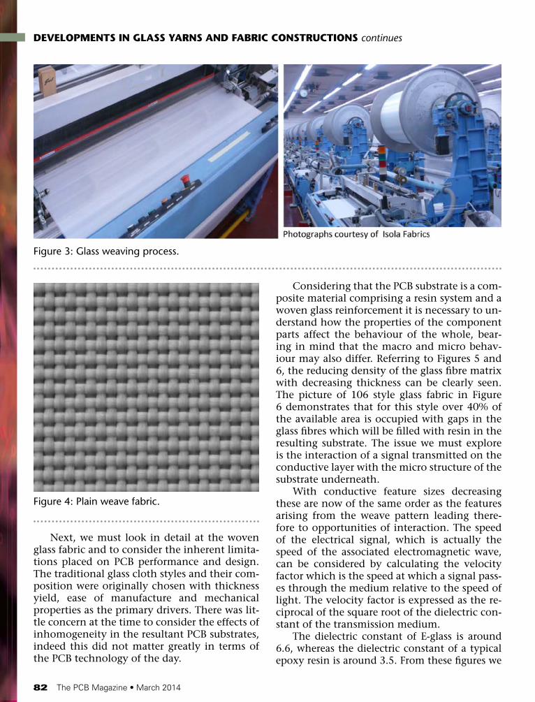
The first part of the weaving process is called warping, which is the operation through which the yarn on the bobbins is transferred to section beams at the required spacing to form the warp threads which run in the machine direction and are up to 3 kilometres in length. Depend-ing on the total number of threads required for a given type of glass weave (style), several sec-tional beams are produced and consolidated in a group called a set which is the input for the slashing process where additional size is added to protect the fibres from breakage through the weaving process.
Once the loom beam is installed on the weaving loom, fabric is formed by interlacing filling yarns (picks, weft threads) orthogonal to warp threads (ends) (Figure 3); the most com-mon interlacing of fill and warp ends (weave
pattern) is plain weave although others such as basket, twill and satin are available. The woven fabric is wound onto a roll for subsequent heat cleaning to remove the size and then onto fin-ishing operations.
In order to provide maximum adhesion of the fabric to the various resins matrices, a coupling agent (finish) is applied to the fabric by impregnating in a “finish bath”; additionally proprietary fibre spreading treatments can also be applied at this stage. The resultant plain weave fabric is shown in Figure 4.
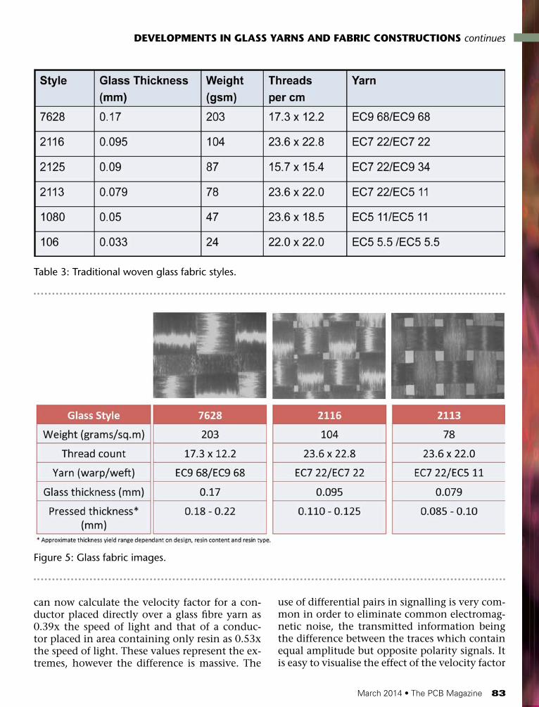
Different yarns are combined in different combinations to weave the variety of “styles” that are subsequently used for PCB substrate production. Table 3 shows the composition of the traditional styles available.
table 2: glass yarn common types.
Figure 2: glass yarn designation.
DEVELOPMENTS IN GLASS YARNS AND FABRIC CONSTRUCTIONS continues
82 The PCB Magazine • March 2014
Next, we must look in detail at the woven glass fabric and to consider the inherent limita-tions placed on PCB performance and design. The traditional glass cloth styles and their com-position were originally chosen with thickness yield, ease of manufacture and mechanical properties as the primary drivers. There was lit-tle concern at the time to consider the effects of inhomogeneity in the resultant PCB substrates, indeed this did not matter greatly in terms of the PCB technology of the day.
Considering that the PCB substrate is a com-posite material comprising a resin system and a woven glass reinforcement it is necessary to un-derstand how the properties of the component parts affect the behaviour of the whole, bear-ing in mind that the macro and micro behav-iour may also differ. Referring to Figures 5 and 6, the reducing density of the glass fibre matrix with decreasing thickness can be clearly seen. The picture of 106 style glass fabric in Figure 6 demonstrates that for this style over 40% of the available area is occupied with gaps in the glass fibres which will be filled with resin in the resulting substrate. The issue we must explore is the interaction of a signal transmitted on the conductive layer with the micro structure of the substrate underneath.
With conductive feature sizes decreasing these are now of the same order as the features arising from the weave pattern leading there-fore to opportunities of interaction. The speed of the electrical signal, which is actually the speed of the associated electromagnetic wave, can be considered by calculating the velocity factor which is the speed at which a signal pass-es through the medium relative to the speed of light. The velocity factor is expressed as the re-ciprocal of the square root of the dielectric con-stant of the transmission medium.
The dielectric constant of E-glass is around 6.6, whereas the dielectric constant of a typical epoxy resin is around 3.5. From these figures we
Figure 3: glass weaving process.
Figure 4: plain weave fabric.
DEVELOPMENTS IN GLASS YARNS AND FABRIC CONSTRUCTIONS continues
March 2014 • The PCB Magazine 83
can now calculate the velocity factor for a con-ductor placed directly over a glass fibre yarn as 0.39x the speed of light and that of a conduc-tor placed in area containing only resin as 0.53x the speed of light. These values represent the ex-tremes, however the difference is massive. The
use of differential pairs in signalling is very com-mon in order to eliminate common electromag-netic noise, the transmitted information being the difference between the traces which contain equal amplitude but opposite polarity signals. It is easy to visualise the effect of the velocity factor
table 3: traditional woven glass fabric styles.
Figure 5: glass fabric images.
DEVELOPMENTS IN GLASS YARNS AND FABRIC CONSTRUCTIONS continues

84 The PCB Magazine • March 2014
differences explained above on differential pairs; Figure 7 show a differential pair marked “A” and “B”, the “A” trace runs directly over a glass fibre, whereas trace “B” runs over a resin rich area. The
consequent signal velocities mean that these two traces cannot behave as intended as the resultant signals will arrive at their destination skewed, or out of sync. Figure 8 shows the signal from a
Figure 6: glass fabric images.
Figure 7: micro dk effect on differential pair.
DEVELOPMENTS IN GLASS YARNS AND FABRIC CONSTRUCTIONS continues

86 The PCB Magazine • March 2014
Figure 8: eye pattern of perfectly aligned differential pair.
Figure 9: eye pattern with 80 pico second skew.
DEVELOPMENTS IN GLASS YARNS AND FABRIC CONSTRUCTIONS continues

March 2014 • The PCB Magazine 87
perfectly aligned differential pair, Figure 9 shows the effect of only 80ps of skew to the signal, the reader can see that the eye is almost completely closed leading to a loss of signal integrity.
Early efforts to mitigate this effect relied on rotating the circuitry relative to the weave pat-tern in order to provide an equal path constitu-tion for both parts of the differential pair. How-ever this proved to be an expensive solution as it resulted in large amounts of material wastage in panelisation inefficiency.
There are a number of techniques directly related to the glass fabric that can be used to mitigate and even completely eliminate this effect. The first relies on altering the glass fab-ric construction in order to close up the gaps between the glass yarns. The effect is to pres-ent the conductor with a more homogeneous substrate over which to pass thus minimising the micro Dk effects described above. In recent years a number of traditional glass cloth styles have been substituted by a “square weave” al-ternative. The square weave alternative adds ad-ditional glass yarns and balances up the warp and weft directions so that they have the same, or nearly the same, thread count in the warp and weft direction. Table 4 shows the construc-tion of some popular square weave glass cloth styles.
There are further techniques that effec-tively spread the glass fibres out so that they
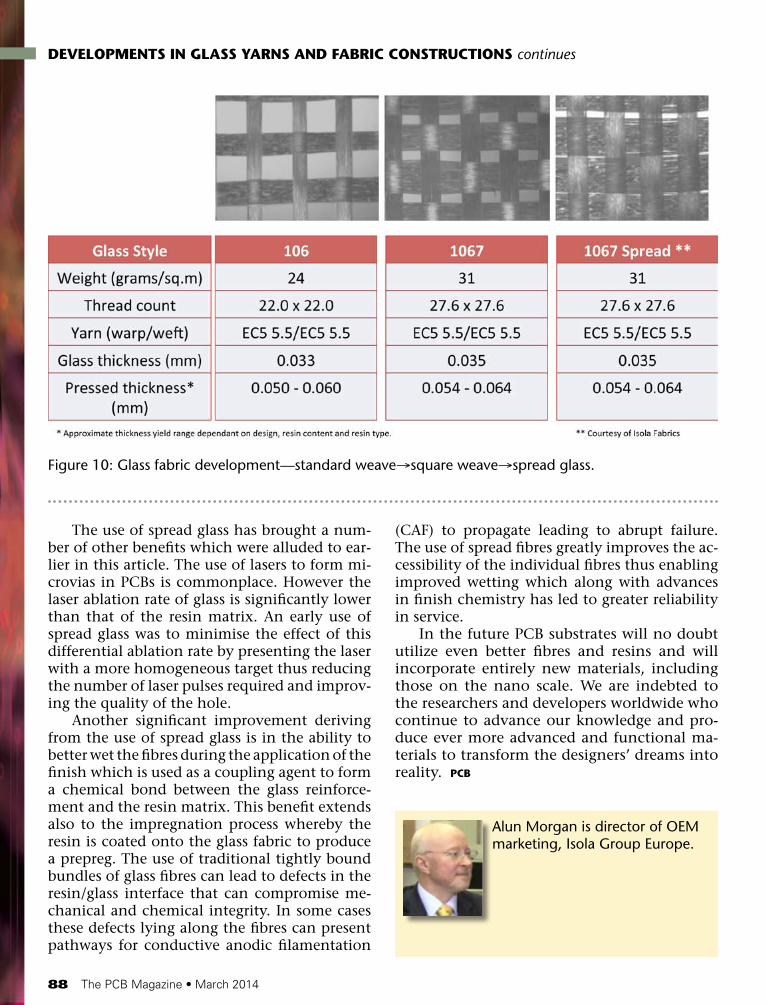
lay flatter and no longer remain in tightly twisted threads thus distributing the avail-able fibres into the gaps between the threads. A number of methods have been employed in recent years to produce this effect; some rely on a change to the yarn production and weaving process, some to an additional post weaving process and some to a combination of techniques. Figure 10 shows photomicro-graphs of standard 106 style glass, the square weave version 1067 and finally a spread glass version of 1067. The reader can clearly see how the large gaps in the standard 106 glass fabric have been all but eliminated in the spread glass version.
There is now also a novel solution by which skew can be all but eliminated. Isola’s newly developed GigaSync™ product offers laminates and prepregs with engineered glass weaves hav-ing the same dielectric constant as the resin sys-tem. Matching the Dk of both component parts of the composite substrate means the elimina-tion of the skew effect as the micro composi-tion of the substrate can no longer introduce variability to the signal path. This applies to all combinations of glass styles used in a stack-up as the resin content no longer has an influence on the dielectric constant thus simplifying the electrical design. This innovation is an enabler to achieve data transmission rates of 100 Gbps and beyond.
table 4: selected square-weave woven glass fabrics.
DEVELOPMENTS IN GLASS YARNS AND FABRIC CONSTRUCTIONS continues
88 The PCB Magazine • March 2014
The use of spread glass has brought a num-ber of other benefits which were alluded to ear-lier in this article. The use of lasers to form mi-crovias in PCBs is commonplace. However the laser ablation rate of glass is significantly lower than that of the resin matrix. An early use of spread glass was to minimise the effect of this differential ablation rate by presenting the laser with a more homogeneous target thus reducing the number of laser pulses required and improv-ing the quality of the hole.
Another significant improvement deriving from the use of spread glass is in the ability to better wet the fibres during the application of the finish which is used as a coupling agent to form a chemical bond between the glass reinforce-ment and the resin matrix. This benefit extends also to the impregnation process whereby the resin is coated onto the glass fabric to produce a prepreg. The use of traditional tightly bound bundles of glass fibres can lead to defects in the resin/glass interface that can compromise me-chanical and chemical integrity. In some cases these defects lying along the fibres can present pathways for conductive anodic filamentation
(CAF) to propagate leading to abrupt failure. The use of spread fibres greatly improves the ac-cessibility of the individual fibres thus enabling improved wetting which along with advances in finish chemistry has led to greater reliability in service.
In the future PCB substrates will no doubt utilize even better fibres and resins and will incorporate entirely new materials, including those on the nano scale. We are indebted to the researchers and developers worldwide who continue to advance our knowledge and pro-duce ever more advanced and functional ma-terials to transform the designers’ dreams into reality. PCB
Figure 10: glass fabric development—standard weave→square weave→spread glass.
alun morgan is director of oem marketing, isola group europe.
DEVELOPMENTS IN GLASS YARNS AND FABRIC CONSTRUCTIONS continues