Embed Size (px)
Citation preview
FOR MESSRS : DATE : Jun. 10th ,2019
CUSTOMER’S ACCEPTANCE SPECIFICATIONS
TX17D01VM2CAA
Contents
No. ITEM SHEET No. PAGE
1 COVER 7B64PS 2701-TX17D01VM2CAA-7 1-1/1
2 RECORD OF REVISION 7B64PS 2702-TX17D01VM2CAA-7 2-1/3~3/3
3 GENERAL DATA 7B64PS 2703-TX17D01VM2CAA-7 3-1/1
4 ABSOLUTE MAXIMUM RATINGS 7B64PS 2704-TX17D01VM2CAA-7 4-1/1
5 ELECTRICAL CHARACTERISTICS 7B64PS 2705-TX17D01VM2CAA-7 5-1/1
6 OPTICAL CHARACTERISTICS 7B64PS 2706-TX17D01VM2CAA-7 6-1/2~2/2
7 BLOCK DIAGRAME 7B64PS 2707-TX17D01VM2CAA-7 7-1/1
8 RELIABILITY TESTS 7B64PS 2708-TX17D01VM2CAA-7 8-1/1
9 LCD INTERFACE 7B64PS 2709-TX17D01VM2CAA-7 9-1/7~7/7
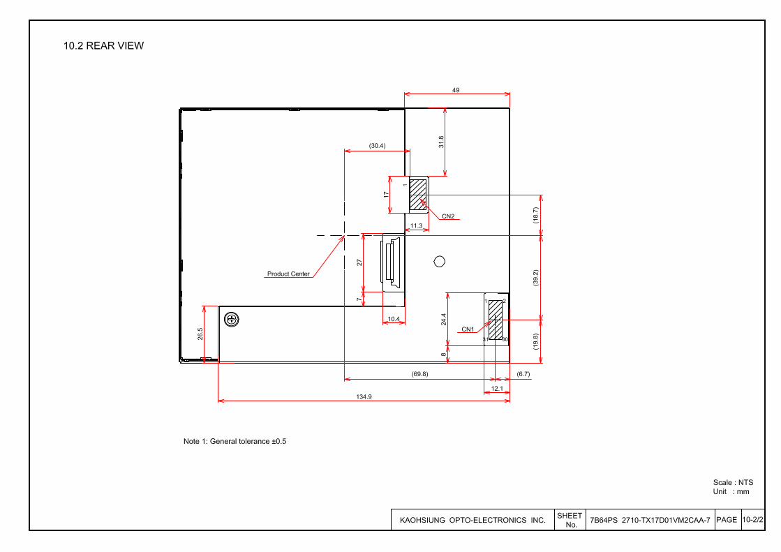
10 OUTLINE DIMENSIONS 7B64PS 2710-TX17D01VM2CAA-7 10-1/2~2/2
11 APPEARANCE STANDARD 7B64PS 2711-TX17D01VM2CAA-7 11-1/3~3/3
12 PRECAUTIONS 7B64PS 2712-TX17D01VM2CAA-7 12-1/2~2/2
13 DESIGNATION OF LOT MARK 7B64PS 2713-TX17D01VM2CAA-7 13-1/1
ACCEPTED BY: PROPOSED BY:
KAOHSIUNG OPTO-ELECTRONICS INC. SHEETNO. 7B64PS 2701-TX17D01VM2CAA-7 PAGE 1-1/1
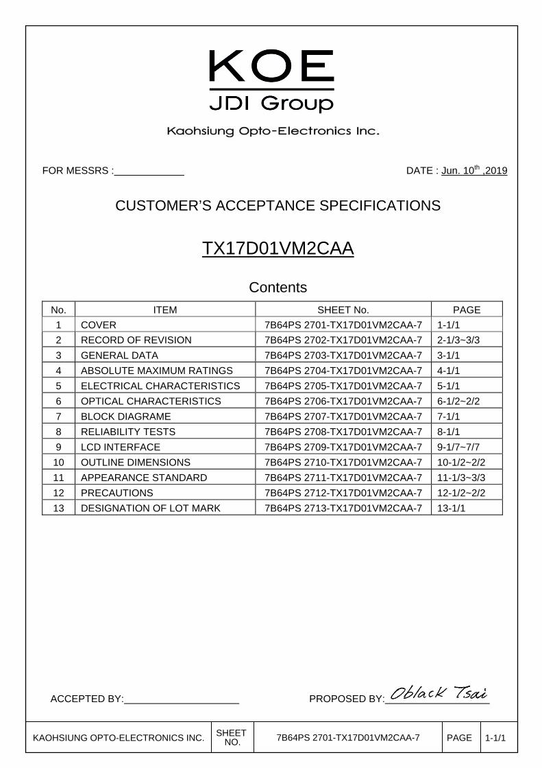
2. RECORD OF REVISION
DATE SHEET No. SUMMARY Jun.26,’09 7B64PS 2703 –
TX17D01VM2CAA-2
Page 3 - 1/1
3.1 DISPLAY FEATURES
Revised :
Power Consumption : 0.42 W for LCD → 0.47 W for LCD
7B64PS 2705 –
TX17D01VM2CAA-2
Page 5 - 1/1
5.1 LCD CHARACTERISTICS
Revised
Item Min. Typ. Max.
Power Supply Current 100 125 150
↓
Item Min. Typ. Max.
Power Supply Current 116 145 174
7B64PS 2710 –
TX17D01VM2CAA-2
Page 10 - 2/2
10.2 BACK SIDE
All Sheet Revised.
Feb.11,’10 7B64PS 2703 –
TX17D01VM2CAA-3
Page 3 - 1/1
3.1 DISPLAY FEATURES
Revised :
Power Consumption : 0.47 W for LCD → 0.36 W for LCD
7B64PS 2705 –
TX17D01VM2CAA-3
Page 5 - 1/1
5.1 LCD CHARACTERISTICS
Revised :
Item Min. Typ. Max.
Power Supply Current 116 145 174
Vsync Frequency 54 60 66
↓
Item Min. Typ. Max.
Power Supply Current - 110 135
Vsync Frequency - 60 66
Added : Note 3
7B64PS 2708 –
TX17D01VM2CAA-3
Page 8 - 1/1
8. RELIABILITY
Revised :
Test Item Condition
Vibration 3) 3G
↓
Test Item Condition
Vibration 3) 2G
Deleted :
Test Item Condition
ESD 5) 3)
Added : Note 4
KAOHSIUNG OPTO-ELECTRONICS INC. SHEET
NO. 7B64PS 2702-TX17D01VM2CAA-7 PAGE 2-1/3
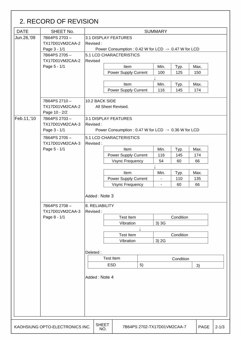
DATE SHEET No. SUMMARY May 01,’12 All pages Company name changed:
KAOHSIUNG HITACHI ELECTRONICS CO.,LTD.
KAOHSIUNG OPTO-ELECTRONICS INC. 7B64PS-2704- TX17D01VM2CAA-4 Page 4-1/1
4. ABSOLUTE MAXIMUM RATINGS Revised : Note2.
Jun. 08,’12 7B64PS-2703- TX17D01VM2CAA-5 Page 3-1/1
3.1 DISPLAY FEATURES
Revised :
Power Consumption : 0.36 W for LCD → 0.48 W for LCD
7B64PS-2705- TX17D01VM2CAA-5 Page 5-1/1
5.1 LCD CHARACTERISTICS
Revised :
Item Typ. Max.
Power Supply Current 110 135
↓
Item Typ. Max.
Power Supply Current 144 172
7B64PS-2713- TX17D01VM2CAA-5 Page 13-1/1
13. DESIGNATION of LOT MARK
Added : REV.No ITEM REMARKS
- - -
A DC/DC converter changed PCN 0850
Revised :
↓
Aug.29,’17 7B64PS-2713-
TX17D01VM2CAA-6 Page 13-1/1
13. DESIGNATION of LOT MARK
Added : REV.No ITEM REMARKS
B LCD source changed PCN 0976
KAOHSIUNG OPTO-ELECTRONICS INC. SHEET
NO. 7B64PS 2702-TX17D01VM2CAA-7 PAGE 2-2/3
TX17D01VM2CAA 9044T (5D) 005373
REV:
KOE MADE IN TAIWAN
TX17D01VM2CAA 9044T (5E) 005373
REV: A
KOE MADE IN TAIWAN
→
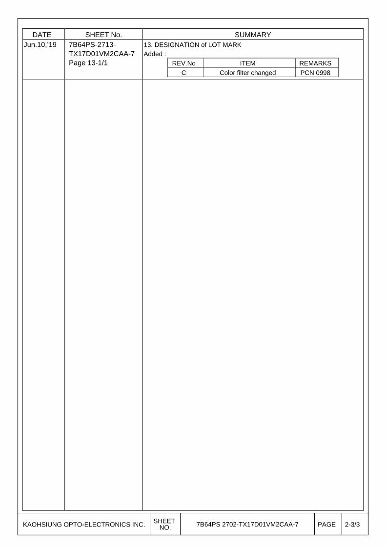
DATE SHEET No. SUMMARY Jun.10,’19 7B64PS-2713-
TX17D01VM2CAA-7 Page 13-1/1
13. DESIGNATION of LOT MARK
Added : REV.No ITEM REMARKS
C Color filter changed PCN 0998
KAOHSIUNG OPTO-ELECTRONICS INC. SHEET
NO. 7B64PS 2702-TX17D01VM2CAA-7 PAGE 2-3/3
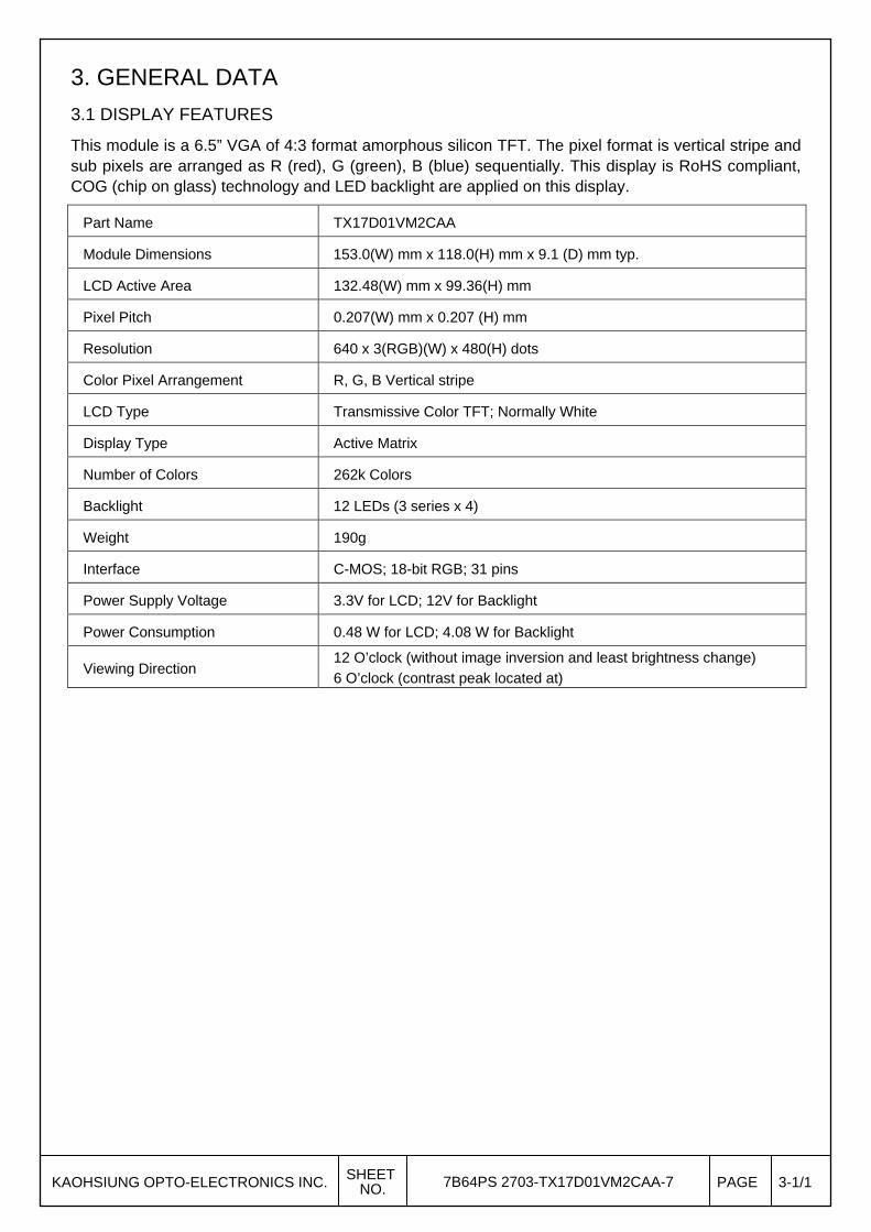
3. GENERAL DATA
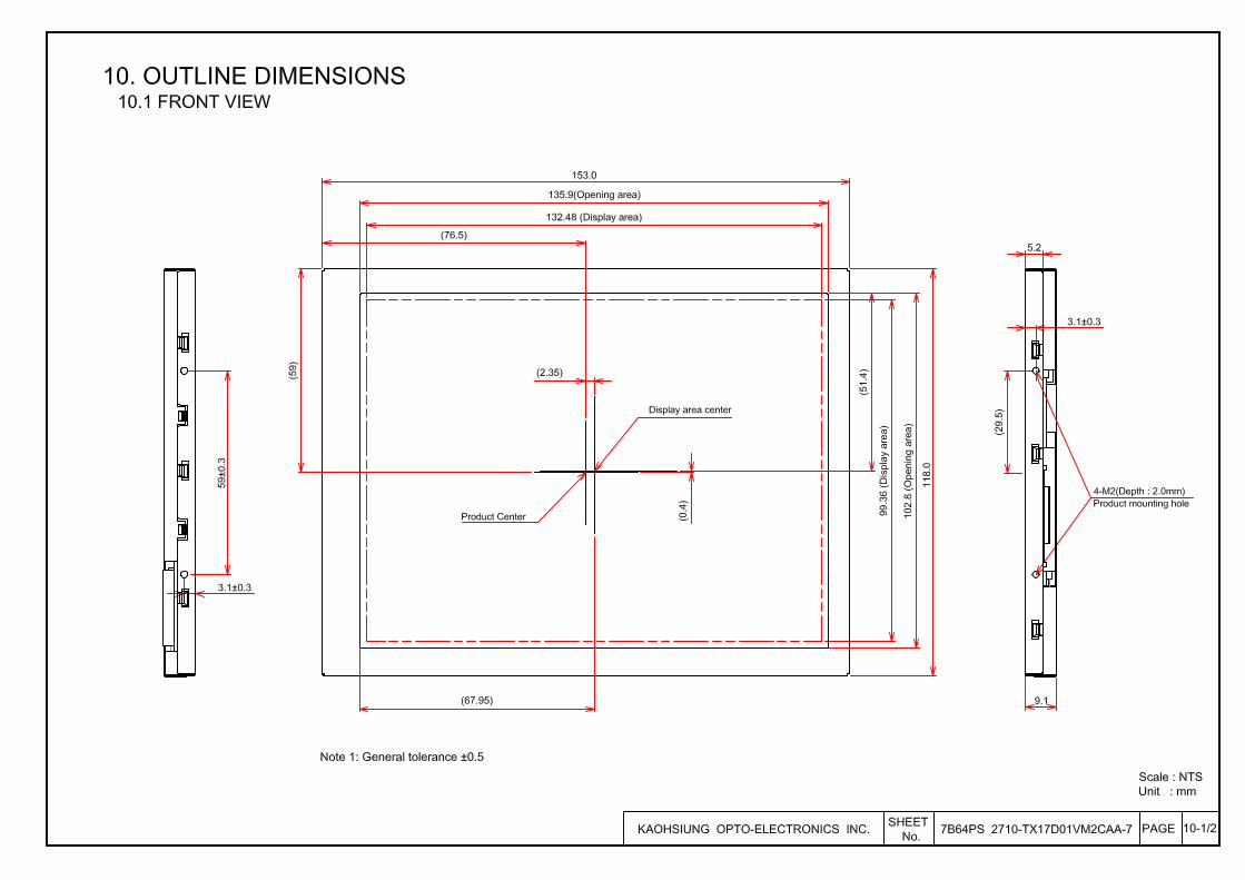
3.1 DISPLAY FEATURES
This module is a 6.5” VGA of 4:3 format amorphous silicon TFT. The pixel format is vertical stripe and sub pixels are arranged as R (red), G (green), B (blue) sequentially. This display is RoHS compliant, COG (chip on glass) technology and LED backlight are applied on this display.
Part Name TX17D01VM2CAA
Module Dimensions 153.0(W) mm x 118.0(H) mm x 9.1 (D) mm typ.
LCD Active Area 132.48(W) mm x 99.36(H) mm
Pixel Pitch 0.207(W) mm x 0.207 (H) mm
Resolution 640 x 3(RGB)(W) x 480(H) dots
Color Pixel Arrangement R, G, B Vertical stripe
LCD Type Transmissive Color TFT; Normally White
Display Type Active Matrix
Number of Colors 262k Colors
Backlight 12 LEDs (3 series x 4)
Weight 190g
Interface C-MOS; 18-bit RGB; 31 pins
Power Supply Voltage 3.3V for LCD; 12V for Backlight
Power Consumption 0.48 W for LCD; 4.08 W for Backlight
Viewing Direction 12 O’clock (without image inversion and least brightness change)
6 O’clock (contrast peak located at)
KAOHSIUNG OPTO-ELECTRONICS INC. SHEETNO. 7B64PS 2703-TX17D01VM2CAA-7 PAGE 3-1/1
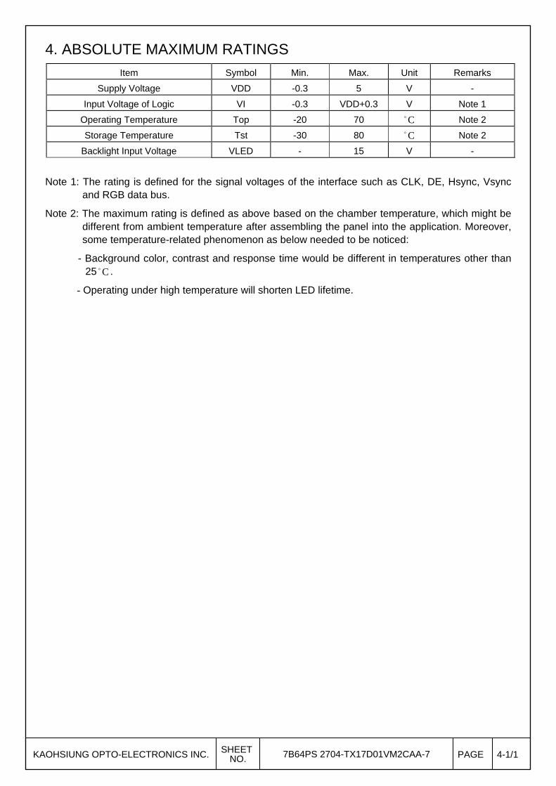
4. ABSOLUTE MAXIMUM RATINGS
Item Symbol Min. Max. Unit Remarks
Supply Voltage VDD -0.3 5 V -
Input Voltage of Logic VI -0.3 VDD+0.3 V Note 1
Operating Temperature Top -20 70 C Note 2
Storage Temperature Tst -30 80 C Note 2
Backlight Input Voltage VLED - 15 V -
Note 1: The rating is defined for the signal voltages of the interface such as CLK, DE, Hsync, Vsync and RGB data bus.
Note 2: The maximum rating is defined as above based on the chamber temperature, which might be different from ambient temperature after assembling the panel into the application. Moreover, some temperature-related phenomenon as below needed to be noticed:
- Background color, contrast and response time would be different in temperatures other than 25 C .
- Operating under high temperature will shorten LED lifetime.
KAOHSIUNG OPTO-ELECTRONICS INC. SHEETNO. 7B64PS 2704-TX17D01VM2CAA-7 PAGE 4-1/1
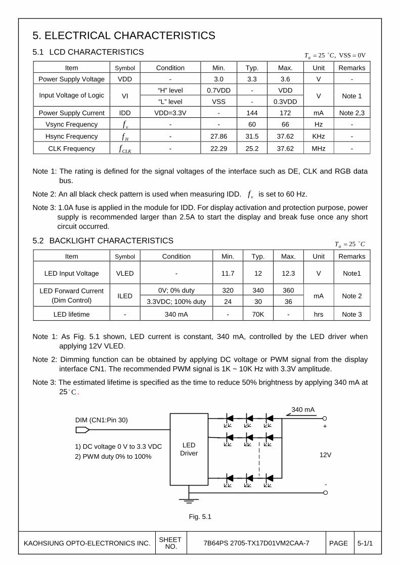
5. ELECTRICAL CHARACTERISTICS
5.1 LCD CHARACTERISTICS
Item Symbol Condition Min. Typ. Max. Unit Remarks
Power Supply Voltage VDD - 3.0 3.3 3.6 V -
Input Voltage of Logic VI “H” level 0.7VDD - VDD
V Note 1 “L” level VSS - 0.3VDD
Power Supply Current IDD VDD=3.3V - 144 172 mA Note 2,3
Vsync Frequency vf - - 60 66 Hz -
Hsync Frequency Hf - 27.86 31.5 37.62 KHz -
CLK Frequency CLKf - 22.29 25.2 37.62 MHz -
Note 1: The rating is defined for the signal voltages of the interface such as DE, CLK and RGB data bus.
Note 2: An all black check pattern is used when measuring IDD. vf is set to 60 Hz.
Note 3: 1.0A fuse is applied in the module for IDD. For display activation and protection purpose, power supply is recommended larger than 2.5A to start the display and break fuse once any short circuit occurred.
5.2 BACKLIGHT CHARACTERISTICS
Item Symbol Condition Min. Typ. Max. Unit Remarks
LED Input Voltage VLED - 11.7 12 12.3 V Note1
LED Forward Current
(Dim Control) ILED
0V; 0% duty 320 340 360 mA Note 2
3.3VDC; 100% duty 24 30 36
LED lifetime - 340 mA - 70K - hrs Note 3
Note 1: As Fig. 5.1 shown, LED current is constant, 340 mA, controlled by the LED driver when applying 12V VLED.
Note 2: Dimming function can be obtained by applying DC voltage or PWM signal from the display interface CN1. The recommended PWM signal is 1K ~ 10K Hz with 3.3V amplitude.
Note 3: The estimated lifetime is specified as the time to reduce 50% brightness by applying 340 mA at 25 C .
LEDDriver
DIM (CN1:Pin 30)+
-
12V
340 mA
1) DC voltage 0 V to 3.3 VDC
2) PWM duty 0% to 100%
Fig. 5.1
0VVSS ,25 CTa
CTa25
KAOHSIUNG OPTO-ELECTRONICS INC. SHEETNO. 7B64PS 2705-TX17D01VM2CAA-7 PAGE 5-1/1
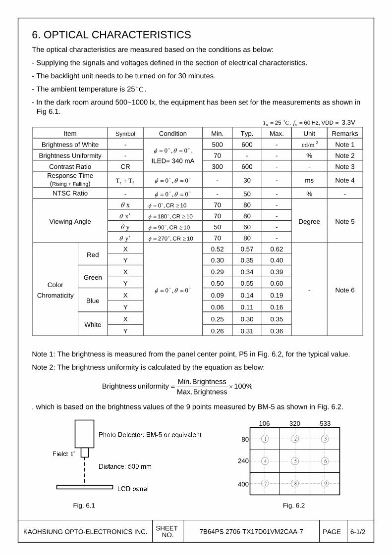
6. OPTICAL CHARACTERISTICS The optical characteristics are measured based on the conditions as below:
- Supplying the signals and voltages defined in the section of electrical characteristics.
- The backlight unit needs to be turned on for 30 minutes.
- The ambient temperature is 25 C .
- In the dark room around 500~1000 lx, the equipment has been set for the measurements as shown in Fig 6.1.
3.3V
Item Symbol Condition Min. Typ. Max. Unit Remarks
Brightness of White - 0 ,0 ,
ILED= 340 mA
500 600 - 2cd/m Note 1
Brightness Uniformity - 70 - - % Note 2
Contrast Ratio CR 300 600 - - Note 3 Response Time (Rising + Falling) fr T T 0 ,0 - 30 - ms Note 4
NTSC Ratio - 0 ,0 - 50 - % -
Viewing Angle
x 10 CR ,0 70 80 -
Degree Note 5 x 10 CR ,180 70 80 -
y 10 CR ,90 50 60 -
y 10 CR ,270 70 80 -
Color
Chromaticity
Red X
0 ,0
0.52 0.57 0.62
- Note 6
Y 0.30 0.35 0.40
Green X 0.29 0.34 0.39
Y 0.50 0.55 0.60
Blue X 0.09 0.14 0.19
Y 0.06 0.11 0.16
White X 0.25 0.30 0.35
Y 0.26 0.31 0.36
Note 1: The brightness is measured from the panel center point, P5 in Fig. 6.2, for the typical value.
Note 2: The brightness uniformity is calculated by the equation as below:
100% Brightness Max.
Brightness Min.uniformity Brightness
, which is based on the brightness values of the 9 points measured by BM-5 as shown in Fig. 6.2.
1
106 320 533
80
240
400
1 2 3
4 5 6
7 8 9
Fig. 6.1 Fig. 6.2
VDDHz, 60 25 va fCT ,
KAOHSIUNG OPTO-ELECTRONICS INC. SHEETNO. 7B64PS 2706-TX17D01VM2CAA-7 PAGE 6-1/2
Note 3: The Contrast Ratio is measured from the center point of the panel, P5, and defined as the following equation:
100% x Black of Brightness
Whiteof Brightness CR
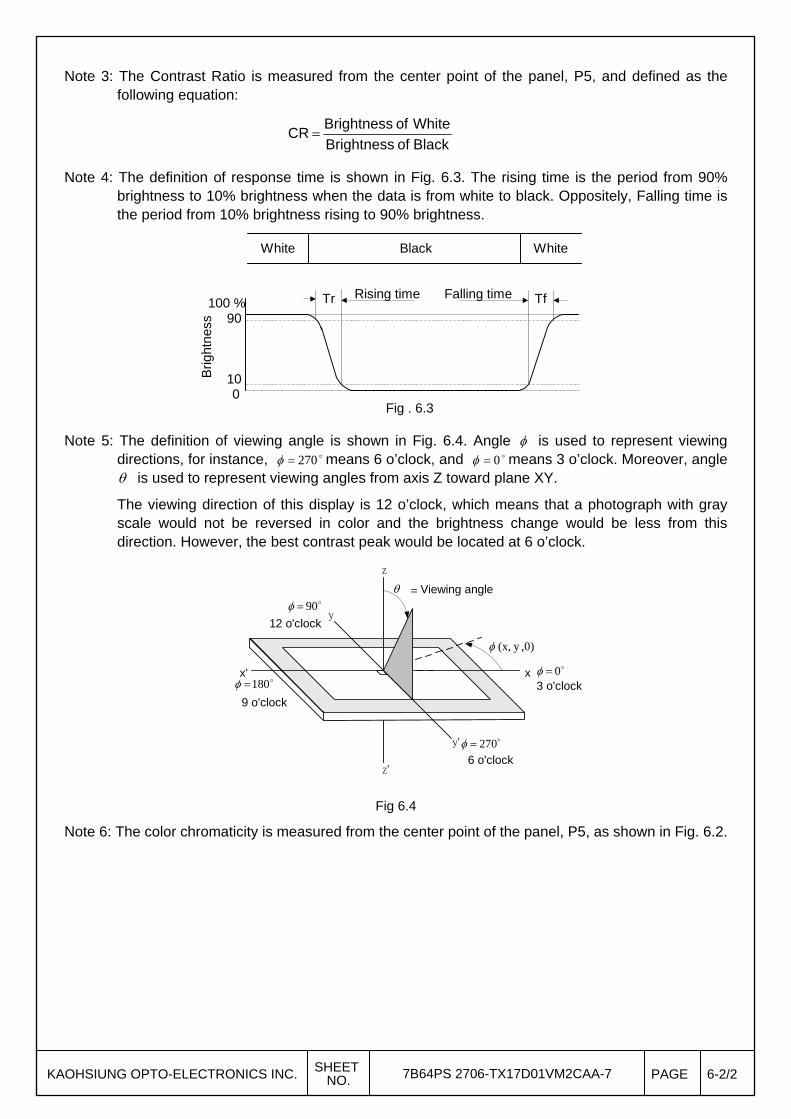
Note 4: The definition of response time is shown in Fig. 6.3. The rising time is the period from 90% brightness to 10% brightness when the data is from white to black. Oppositely, Falling time is the period from 10% brightness rising to 90% brightness.
WhiteWhite Black
010
90100 %
Brig
htne
ss
Tr TfRising time Falling time
Fig . 6.3
Note 5: The definition of viewing angle is shown in Fig. 6.4. Angle is used to represent viewing directions, for instance, 270 means 6 o’clock, and 0 means 3 o’clock. Moreover, angle is used to represent viewing angles from axis Z toward plane XY.
The viewing direction of this display is 12 o’clock, which means that a photograph with gray scale would not be reversed in color and the brightness change would be less from this direction. However, the best contrast peak would be located at 6 o’clock.
3 o'clockxx'
y
y'
z
z'
,0)y (x,
0
90
180
270 6 o'clock
12 o'clock
9 o'clock
= Viewing angle
Fig 6.4
Note 6: The color chromaticity is measured from the center point of the panel, P5, as shown in Fig. 6.2.
KAOHSIUNG OPTO-ELECTRONICS INC. SHEETNO. 7B64PS 2706-TX17D01VM2CAA-7 PAGE 6-2/2
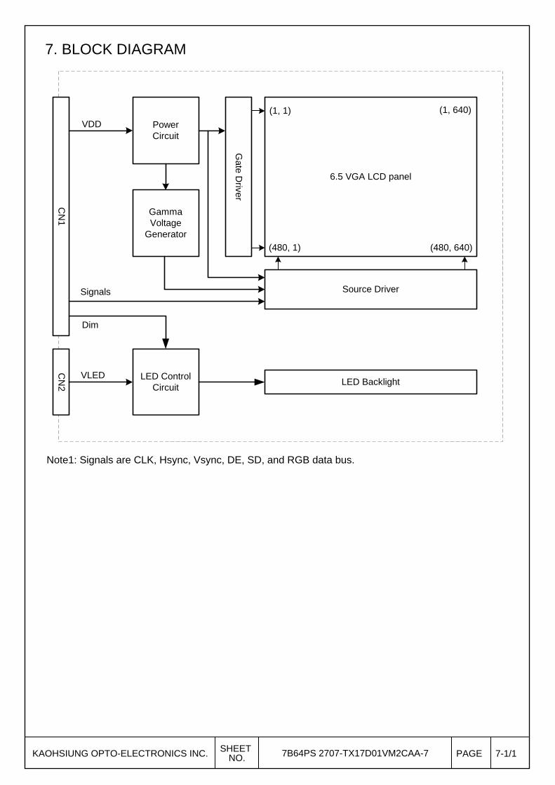
7. BLOCK DIAGRAM
6.5 VGA LCD panel
Source Driver
Gate D
river
CN
1C
N2
LED ControlCircuit
PowerCircuit
GammaVoltage
Generator
VDD
(480, 1) (480, 640)
(1, 640)
LED Backlight
Signals
Dim
VLED
(1, 1)
Note1: Signals are CLK, Hsync, Vsync, DE, SD, and RGB data bus.
KAOHSIUNG OPTO-ELECTRONICS INC. SHEETNO. 7B64PS 2707-TX17D01VM2CAA-7 PAGE 7-1/1
8. RELIABILITY TESTS
Test Item Condition
High Temperature 1) Operating
2) 70 C 240 hrs
Low Temperature 1) Operating
2) -20 C 240 hrs
High Temperature 1) Storage
2) 80 C 240 hrs
Low Temperature 1) Storage
2) -30 C 240 hrs
Heat Cycle 1) Operating
2) –20 C ~70 C
3) 3hrs~1hr~3hrs 240 hrs
Thermal Shock 1) Non-Operating
2) -35 C 85 C
3) 0.5 hr0.5 hr 240 hrs
High Temperature &
Humidity
1) Operating
2) 40 C & 85%RH
3) Without condensation
(Note3)
240 hrs
Vibration
1) Non-Operating
2) 20~200 Hz
3) 2G
4) X, Y, and Z directions
1 hr for each direction
Mechanical Shock
1) Non-Operating
2) 10 ms
3) 50G
4) Y X, and Z directions
Once for each direction
ESD
1) Operating
2) Tip: 200 pF, 250
3) Air discharge for glass: 8KV
4) Contact discharge for metal frame: 8KV
1) Glass: 9 points 2) Metal frame: 8 points(Note4)
Note 1: Display functionalities are inspected under the conditions defined in the specification after the reliability tests.
Note 2: The display is not guaranteed for use in corrosive gas environments.
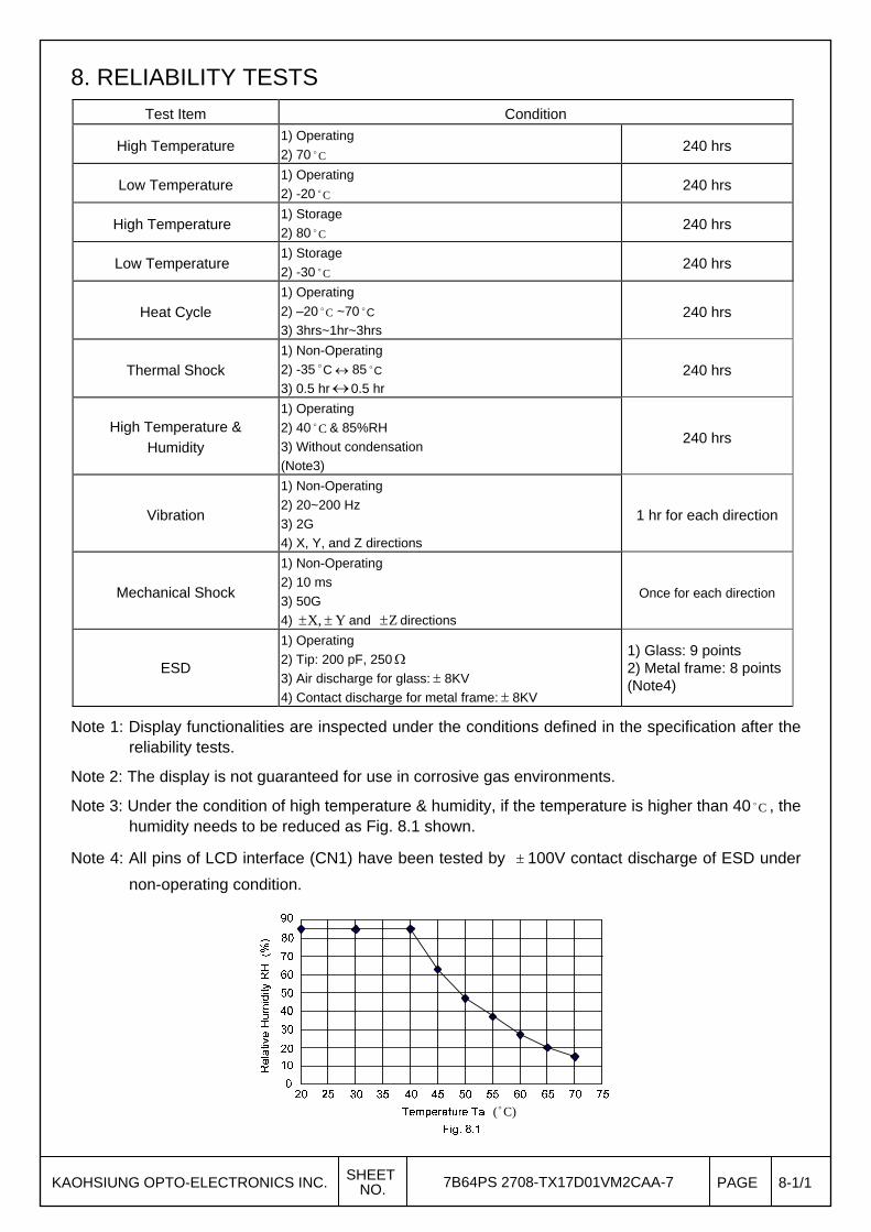
Note 3: Under the condition of high temperature & humidity, if the temperature is higher than 40 C , the humidity needs to be reduced as Fig. 8.1 shown.
Note 4: All pins of LCD interface (CN1) have been tested by 100V contact discharge of ESD under
non-operating condition.
C)(
KAOHSIUNG OPTO-ELECTRONICS INC. SHEET
NO. 7B64PS 2708-TX17D01VM2CAA-7 PAGE 8-1/1
9. LCD INTERFACE
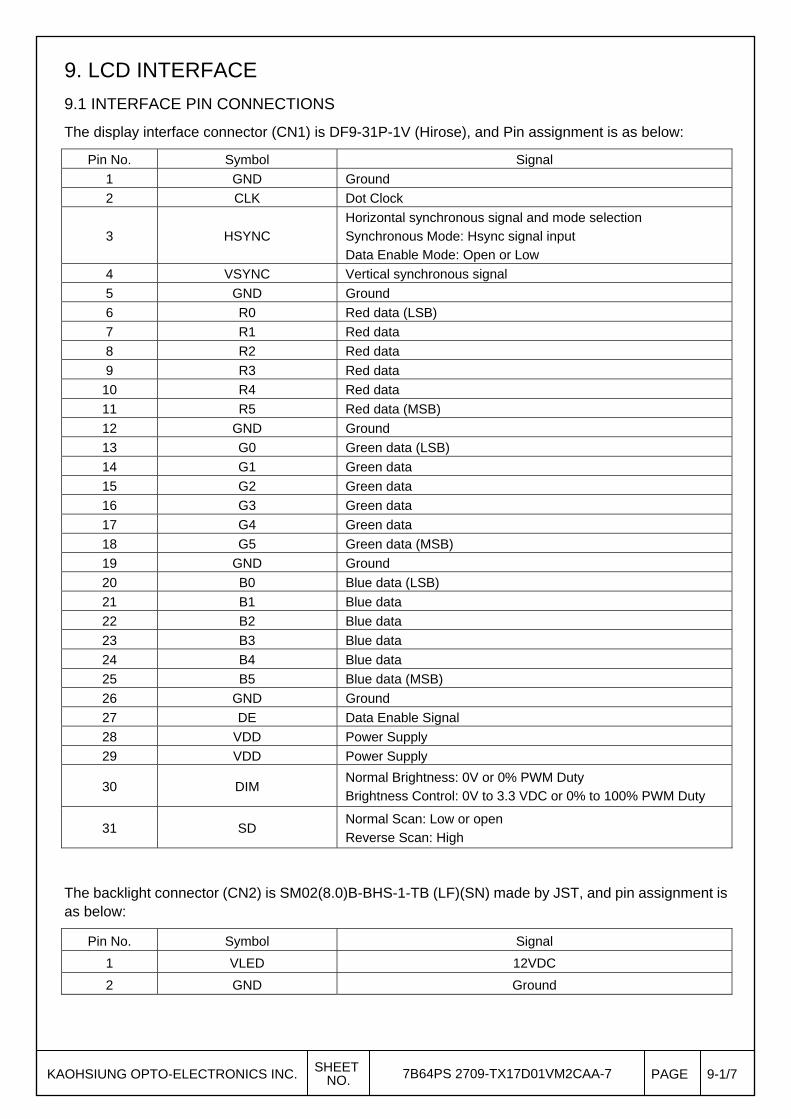
9.1 INTERFACE PIN CONNECTIONS
The display interface connector (CN1) is DF9-31P-1V (Hirose), and Pin assignment is as below:
Pin No. Symbol Signal
1 GND Ground
2 CLK Dot Clock
3 HSYNC
Horizontal synchronous signal and mode selection
Synchronous Mode: Hsync signal input
Data Enable Mode: Open or Low
4 VSYNC Vertical synchronous signal
5 GND Ground
6 R0 Red data (LSB)
7 R1 Red data
8 R2 Red data
9 R3 Red data
10 R4 Red data
11 R5 Red data (MSB)
12 GND Ground
13 G0 Green data (LSB)
14 G1 Green data
15 G2 Green data
16 G3 Green data
17 G4 Green data
18 G5 Green data (MSB)
19 GND Ground
20 B0 Blue data (LSB)
21 B1 Blue data
22 B2 Blue data
23 B3 Blue data
24 B4 Blue data
25 B5 Blue data (MSB)
26 GND Ground
27 DE Data Enable Signal
28 VDD Power Supply
29 VDD Power Supply
30 DIM Normal Brightness: 0V or 0% PWM Duty
Brightness Control: 0V to 3.3 VDC or 0% to 100% PWM Duty
31 SD Normal Scan: Low or open
Reverse Scan: High
The backlight connector (CN2) is SM02(8.0)B-BHS-1-TB (LF)(SN) made by JST, and pin assignment is as below:
Pin No. Symbol Signal
1 VLED 12VDC
2 GND Ground
KAOHSIUNG OPTO-ELECTRONICS INC. SHEETNO. 7B64PS 2709-TX17D01VM2CAA-7 PAGE 9-1/7
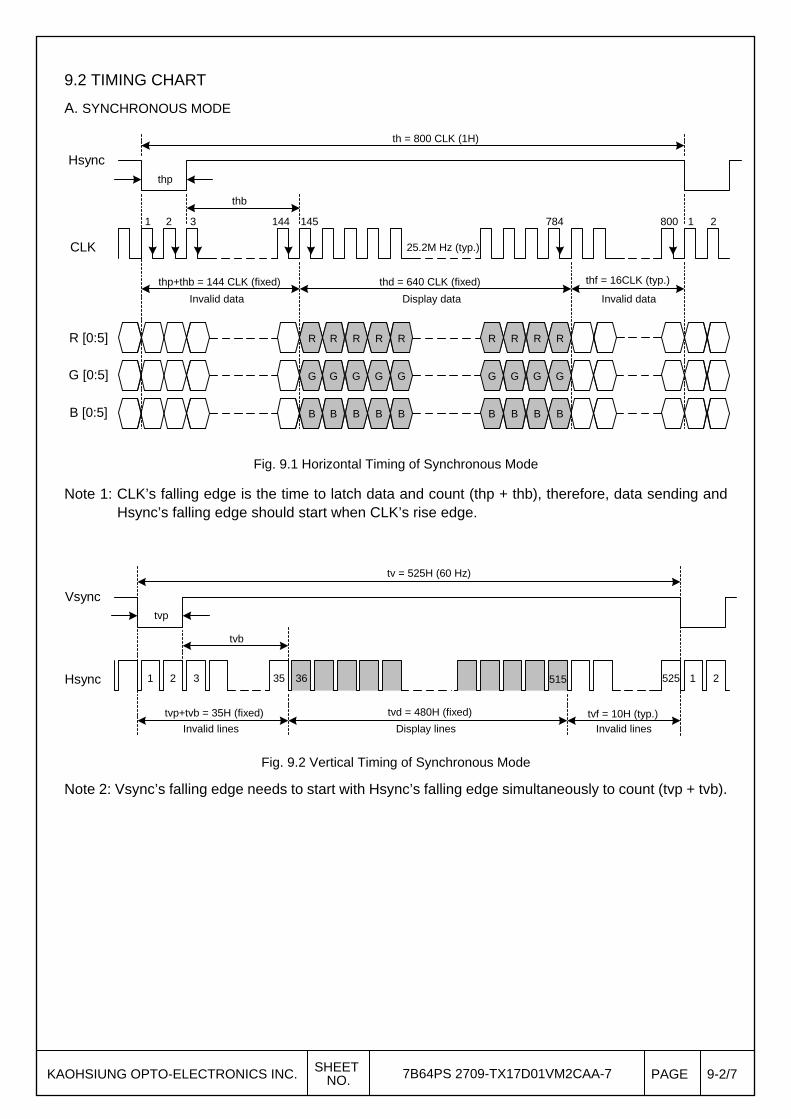
9.2 TIMING CHART
A. SYNCHRONOUS MODE
Hsyncthp
th = 800 CLK (1H)
1 2 3 144
R R R R R R R R R
thb
thp+thb = 144 CLK (fixed) thd = 640 CLK (fixed) thf = 16CLK (typ.)
784 800
Display data
1 2
CLK
G G G G G G G G G
B B B B B B B B B
145
R [0:5]
G [0:5]
B [0:5]
Invalid data Invalid data
25.2M Hz (typ.)
Fig. 9.1 Horizontal Timing of Synchronous Mode
Note 1: CLK’s falling edge is the time to latch data and count (thp + thb), therefore, data sending and Hsync’s falling edge should start when CLK’s rise edge.
1 2 3 35 515 1 2525
tvp+tvb = 35H (fixed) tvd = 480H (fixed) tvf = 10H (typ.)
tvp
tvb
tv = 525H (60 Hz)
Vsync
Hsync
Display lines
36
Invalid lines Invalid lines
Fig. 9.2 Vertical Timing of Synchronous Mode
Note 2: Vsync’s falling edge needs to start with Hsync’s falling edge simultaneously to count (tvp + tvb).
KAOHSIUNG OPTO-ELECTRONICS INC. SHEETNO. 7B64PS 2709-TX17D01VM2CAA-7 PAGE 9-2/7
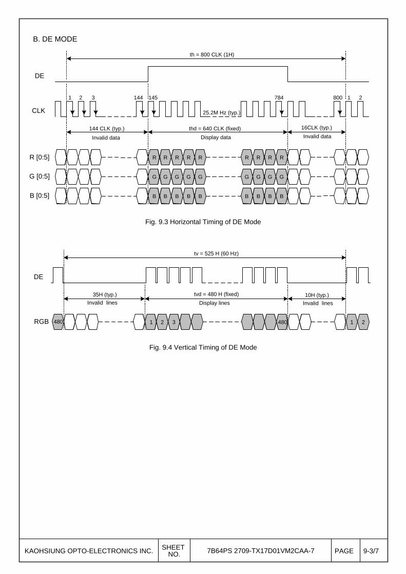
B. DE MODE
DE
th = 800 CLK (1H)
1 2 3 144
R R R R R R R R R
144 CLK (typ.) thd = 640 CLK (fixed) 16CLK (typ.)
784 800
Display data
1 2
CLK
G G G G G G G G G
B B B B B B B B B
145
R [0:5]
G [0:5]
B [0:5]
Invalid data Invalid data
25.2M Hz (typ.)
Fig. 9.3 Horizontal Timing of DE Mode
DE
1 2 3 480
35H (typ.) tvd = 480 H (fixed) 10H (typ.)
Display lines
1 2480
tv = 525 H (60 Hz)
RGB
Invalid lines Invalid lines
Fig. 9.4 Vertical Timing of DE Mode
KAOHSIUNG OPTO-ELECTRONICS INC. SHEETNO. 7B64PS 2709-TX17D01VM2CAA-7 PAGE 9-3/7
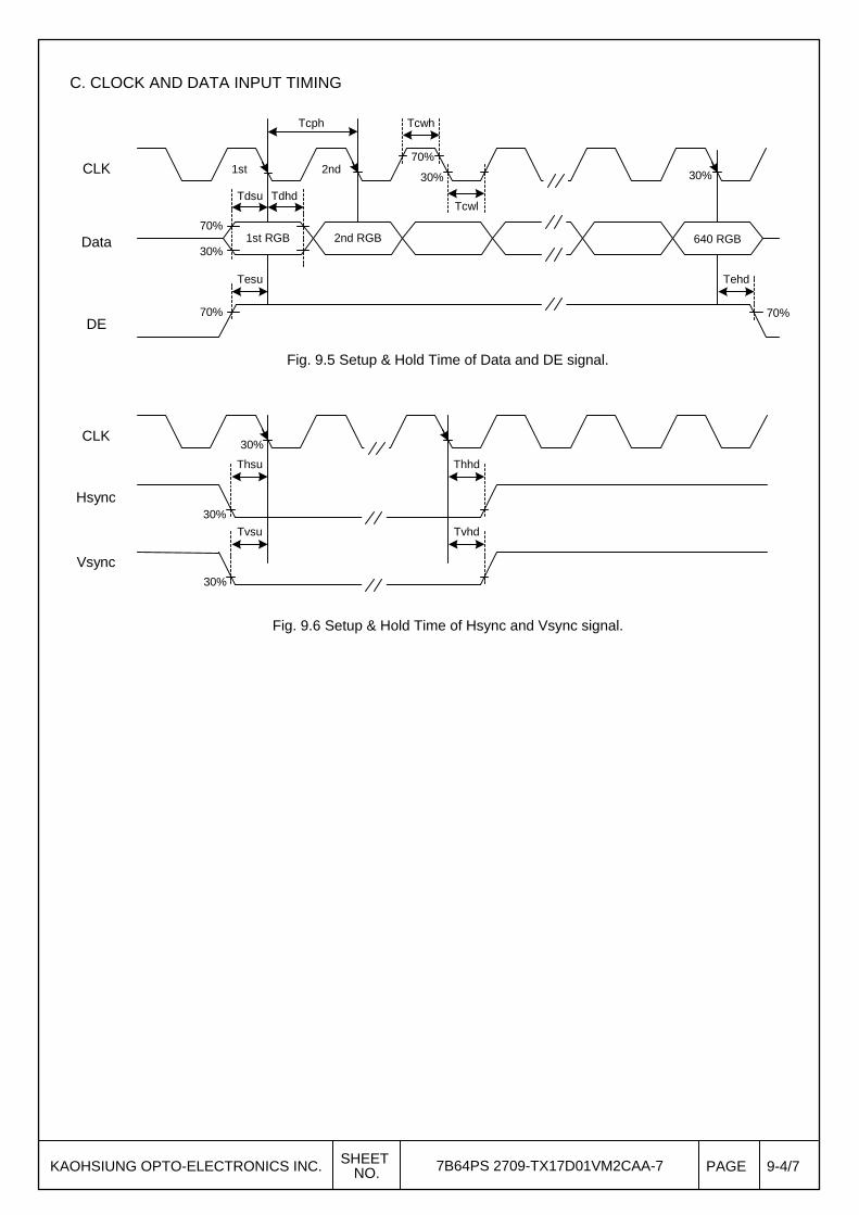
C. CLOCK AND DATA INPUT TIMING
CLK
70%
30%
Tdsu Tdhd
Tcph
1st RGB 2nd RGB
1st 2nd70%
30%
Tcwh
Tcwl
Last Data
30%
70%70%
Tesu Tehd
640 RGBData
DE
Fig. 9.5 Setup & Hold Time of Data and DE signal.
CLK
Thsu Thhd
Tvsu Tvhd
Hsync
Vsync
30%
30%
30%
Fig. 9.6 Setup & Hold Time of Hsync and Vsync signal.
KAOHSIUNG OPTO-ELECTRONICS INC. SHEETNO. 7B64PS 2709-TX17D01VM2CAA-7 PAGE 9-4/7
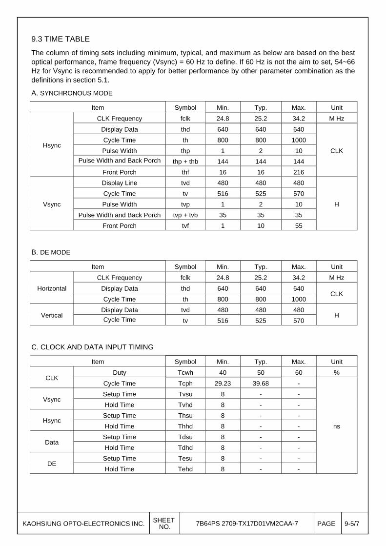
9.3 TIME TABLE
The column of timing sets including minimum, typical, and maximum as below are based on the best optical performance, frame frequency (Vsync) = 60 Hz to define. If 60 Hz is not the aim to set, 54~66 Hz for Vsync is recommended to apply for better performance by other parameter combination as the definitions in section 5.1.
A. SYNCHRONOUS MODE
Item Symbol Min. Typ. Max. Unit
Hsync
CLK Frequency fclk 24.8 25.2 34.2 M Hz
Display Data thd 640 640 640
CLK
Cycle Time th 800 800 1000
Pulse Width thp 1 2 10
Pulse Width and Back Porch thp + thb 144 144 144
Front Porch thf 16 16 216
Vsync
Display Line tvd 480 480 480
H
Cycle Time tv 516 525 570
Pulse Width tvp 1 2 10
Pulse Width and Back Porch tvp + tvb 35 35 35
Front Porch tvf 1 10 55
B. DE MODE
Item Symbol Min. Typ. Max. Unit
Horizontal
CLK Frequency fclk 24.8 25.2 34.2 M Hz
Display Data thd 640 640 640 CLK
Cycle Time th 800 800 1000
Vertical Display Data tvd 480 480 480
H Cycle Time tv 516 525 570
C. CLOCK AND DATA INPUT TIMING
Item Symbol Min. Typ. Max. Unit
CLK Duty Tcwh 40 50 60 %
Cycle Time Tcph 29.23 39.68 -
ns
Vsync Setup Time Tvsu 8 - -
Hold Time Tvhd 8 - -
Hsync Setup Time Thsu 8 - -
Hold Time Thhd 8 - -
Data Setup Time Tdsu 8 - -
Hold Time Tdhd 8 - -
DE Setup Time Tesu 8 - -
Hold Time Tehd 8 - -
KAOHSIUNG OPTO-ELECTRONICS INC. SHEETNO. 7B64PS 2709-TX17D01VM2CAA-7 PAGE 9-5/7
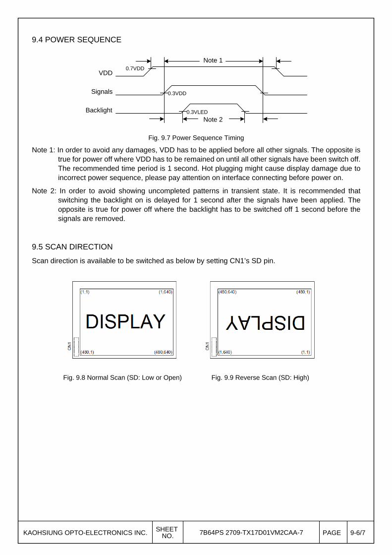
9.4 POWER SEQUENCE
Note 1
Note 2
0.7VDD
0.3VDD
0.3VLED
VDD
Signals
Backlight
Fig. 9.7 Power Sequence Timing
Note 1: In order to avoid any damages, VDD has to be applied before all other signals. The opposite is true for power off where VDD has to be remained on until all other signals have been switch off. The recommended time period is 1 second. Hot plugging might cause display damage due to incorrect power sequence, please pay attention on interface connecting before power on.
Note 2: In order to avoid showing uncompleted patterns in transient state. It is recommended that switching the backlight on is delayed for 1 second after the signals have been applied. The opposite is true for power off where the backlight has to be switched off 1 second before the signals are removed.
9.5 SCAN DIRECTION
Scan direction is available to be switched as below by setting CN1’s SD pin.
Fig. 9.8 Normal Scan (SD: Low or Open) Fig. 9.9 Reverse Scan (SD: High)
KAOHSIUNG OPTO-ELECTRONICS INC. SHEETNO. 7B64PS 2709-TX17D01VM2CAA-7 PAGE 9-6/7
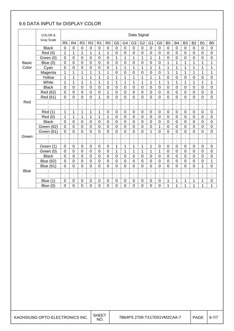
9.6 DATA INPUT for DISPLAY COLOR
COLOR &
Gray Scale Data Signal
R5 R4 R3 R2 R1 R0 G5 G4 G3 G2 G1 G0 B5 B4 B3 B2 B1 B0
Basic Color
Black 0 0 0 0 0 0 0 0 0 0 0 0 0 0 0 0 0 0 Red (0) 1 1 1 1 1 1 0 0 0 0 0 0 0 0 0 0 0 0
Green (0) 0 0 0 0 0 0 1 1 1 1 1 1 0 0 0 0 0 0 Blue (0) 0 0 0 0 0 0 0 0 0 0 0 0 1 1 1 1 1 1
Cyan 0 0 0 0 0 0 1 1 1 1 1 1 1 1 1 1 1 1 Magenta 1 1 1 1 1 1 0 0 0 0 0 0 1 1 1 1 1 1 Yellow 1 1 1 1 1 1 1 1 1 1 1 1 0 0 0 0 0 0 White 1 1 1 1 1 1 1 1 1 1 1 1 1 1 1 1 1 1
Red
Black 0 0 0 0 0 0 0 0 0 0 0 0 0 0 0 0 0 0 Red (62) 0 0 0 0 0 1 0 0 0 0 0 0 0 0 0 0 0 0 Red (61) 0 0 0 0 1 0 0 0 0 0 0 0 0 0 0 0 0 0
: : : : : : : : : : : : : : : : : : : : : : : : : : : : : : : : : : : : : :
Red (1) 1 1 1 1 1 0 0 0 0 0 0 0 0 0 0 0 0 0 Red (0) 1 1 1 1 1 1 0 0 0 0 0 0 0 0 0 0 0 0
Green
Black 0 0 0 0 0 0 0 0 0 0 0 0 0 0 0 0 0 0 Green (62) 0 0 0 0 0 0 0 0 0 0 0 1 0 0 0 0 0 0 Green (61) 0 0 0 0 0 0 0 0 0 0 1 0 0 0 0 0 0 0
: : : : : : : : : : : : : : : : : : : : : : : : : : : : : : : : : : : : : :
Green (1) 0 0 0 0 0 0 1 1 1 1 1 0 0 0 0 0 0 0 Green (0) 0 0 0 0 0 0 1 1 1 1 1 1 0 0 0 0 0 0
Blue
Black 0 0 0 0 0 0 0 0 0 0 0 0 0 0 0 0 0 0 Blue (62) 0 0 0 0 0 0 0 0 0 0 0 0 0 0 0 0 0 1 Blue (61) 0 0 0 0 0 0 0 0 0 0 0 0 0 0 0 0 1 0
: : : : : : : : : : : : : : : : : : : : : : : : : : : : : : : : : : : : : :
Blue (1) 0 0 0 0 0 0 0 0 0 0 0 0 1 1 1 1 1 0 Blue (0) 0 0 0 0 0 0 0 0 0 0 0 0 1 1 1 1 1 1
KAOHSIUNG OPTO-ELECTRONICS INC. SHEETNO. 7B64PS 2709-TX17D01VM2CAA-7 PAGE 9-7/7
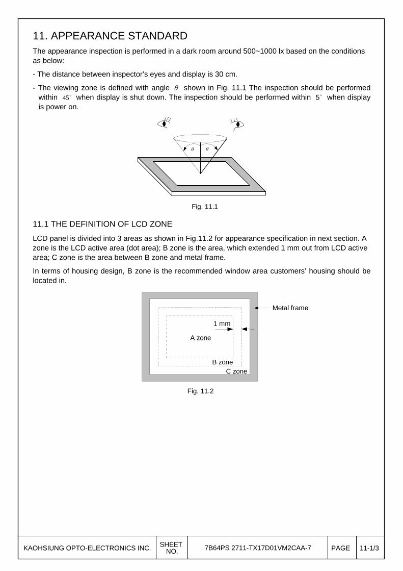
11. APPEARANCE STANDARD The appearance inspection is performed in a dark room around 500~1000 lx based on the conditions as below:
- The distance between inspector’s eyes and display is 30 cm.
- The viewing zone is defined with angle shown in Fig. 11.1 The inspection should be performed within 45 when display is shut down. The inspection should be performed within 5 when display is power on.
Fig. 11.1
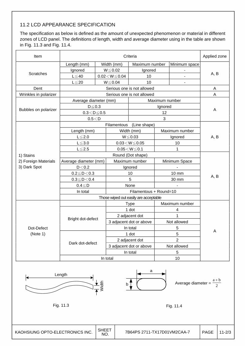
11.1 THE DEFINITION OF LCD ZONE
LCD panel is divided into 3 areas as shown in Fig.11.2 for appearance specification in next section. A zone is the LCD active area (dot area); B zone is the area, which extended 1 mm out from LCD active area; C zone is the area between B zone and metal frame.
In terms of housing design, B zone is the recommended window area customers’ housing should be located in.
Fig. 11.2
A zone
B zoneC zone
Metal frame
1 mm
KAOHSIUNG OPTO-ELECTRONICS INC. SHEETNO. 7B64PS 2711-TX17D01VM2CAA-7 PAGE 11-1/3
11.2 LCD APPEARANCE SPECIFICATION
The specification as below is defined as the amount of unexpected phenomenon or material in different zones of LCD panel. The definitions of length, width and average diameter using in the table are shown in Fig. 11.3 and Fig. 11.4.
Item Criteria Applied zone
Scratches
Length (mm) Width (mm) Maximum number Minimum space
A, B Ignored W≦0.02 Ignored -
L≦40 0.02<W≦0.04 10 -
L≦20 W≦0.04 10 -
Dent Serious one is not allowed A
Wrinkles in polarizer Serious one is not allowed A
Bubbles on polarizer
Average diameter (mm) Maximum number
A D≦0.3 Ignored
0.3<D≦0.5 12
0.5<D 3
1) Stains
2) Foreign Materials
3) Dark Spot
Filamentous (Line shape)
A, B
Length (mm) Width (mm) Maximum number
L≦2.0 W≦0.03 Ignored
L≦3.0 0.03<W≦0.05 10
L≦2.5 0.05<W≦0.1 1
Round (Dot shape)
A, B
Average diameter (mm) Maximum number Minimum Space
D<0.2 Ignored -
0.2≦D<0.3 10 10 mm
0.3≦D<0.4 5 30 mm
0.4≦D None -
In total Filamentous + Round=10
Those wiped out easily are acceptable
Dot-Defect
(Note 1)
Type Maximum number
A
Bright dot-defect
1 dot 4
2 adjacent dot 1
3 adjacent dot or above Not allowed
In total 5
Dark dot-defect
1 dot 5
2 adjacent dot 2
3 adjacent dot or above Not allowed
In total 5
In total 10
Length
Wid
th
Fig. 11.3 Fig. 11.4
a
b Average diameter =2
ba
KAOHSIUNG OPTO-ELECTRONICS INC. SHEETNO. 7B64PS 2711-TX17D01VM2CAA-7 PAGE 11-2/3
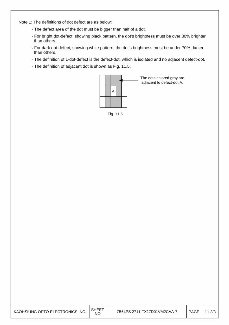
Note 1: The definitions of dot defect are as below:
- The defect area of the dot must be bigger than half of a dot.
- For bright dot-defect, showing black pattern, the dot’s brightness must be over 30% brighter than others.
- For dark dot-defect, showing white pattern, the dot’s brightness must be under 70% darker than others.
- The definition of 1-dot-defect is the defect-dot, which is isolated and no adjacent defect-dot.
- The definition of adjacent dot is shown as Fig. 11.5.
A
The dots colored gray areadjacent to defect-dot A.
Fig. 11.5
KAOHSIUNG OPTO-ELECTRONICS INC. SHEETNO. 7B64PS 2711-TX17D01VM2CAA-7 PAGE 11-3/3
12. PRECAUTIONS
12.1 PRECAUTIONS of ESD
1) Before handling the display, please ensure your body has been connected to ground to avoid any damages by ESD. Also, do not touch display’s interface directly when assembling.
1) Please remove the protection film very slowly before turning on the display to avoid generating ESD.
12.2 PRECAUTIONS of HANDLING
1) In order to keep the appearance of display in good condition, please do not rub any surfaces of the displays by using sharp tools harder than 3H, especially touch panel, metal frame and polarizer.
2) Please do not stack the displays as this may damage the surface. In order to avoid any injuries, please avoid touching the edge of the glass or metal frame and wore gloves during handling.
2) Touching the polarizer or terminal pins with bare hand should be avoided to prevent staining and poor electrical contact.
3) Do not use any harmful chemicals such as acetone, toluene, and isopropyl alcohol to clean display’s surfaces.
4) Please use soft cloth or absorbent cotton with ethanol to clean the display by gently wiping. Moreover, when wiping the display, please wipe it by horizontal or vertical direction instead of circling to prevent leaving scars on the display’s surface, especially polarizer.
5) Please wipe any unknown liquids immediately such as saliva, water or dew on the display to avoid color fading or any permanent damages.
6) Maximum pressure to the surface of the display must be less than 410 x 1,96 Pa. If the area of applied pressure is less than 1 2cm , the maximum pressure must be less than 1.96N.
12.3 PRECAUTIONS OF OPERATING
1) Please input signals and voltages to the displays according to the values defined in the section of electrical characteristics to obtain the best performance. Any voltages over than absolute maximum rating will cause permanent damages to this display. Also, any timing of the signals out of this specification would cause unexpected performance.
2) When the display is operating at significant low temperature, the response time will be slower than it at 25 C . In high temperature, the color will be slightly dark and blue compared to original pattern. However, these are temperature-related phenomenon of LCD and it will not cause permanent damages to the display when used within the operating temperature.
3) The use of screen saver or sleep mode is recommended when static images are likely for long periods of time. This is to avoid the possibility of image sticking.
4) Spike noise can cause malfunction of the circuit. The recommended limitation of spike noise is no bigger than 100 mV.
KAOHSIUNG OPTO-ELECTRONICS INC. SHEETNO. 7B64PS 2712-TX17D01VM2CAA-7 PAGE 12-1/2
12.4 PRECAUTIONS of STORAGE
If the displays are going to be stored for years, please be aware the following notices.
1) Please store the displays in a dark room to avoid any damages from sunlight and other sources of UV light.
2) The recommended long term storage temperature is between 10 C ~35 C and 55%~75% humidity to avoid causing bubbles between polarizer and LCD glasses, and polarizer peeling from LCD glasses.
3) It would be better to keep the displays in the container, which is shipped from KOE, and do not unpack it.
4) Please do not stick any labels on the display surface for a long time, especially on the polarizer.
KAOHSIUNG OPTO-ELECTRONICS INC. SHEETNO. 7B64PS 2712-TX17D01VM2CAA-7 PAGE 12-2/2
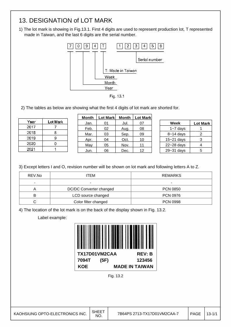
13. DESIGNATION of LOT MARK 1) The lot mark is showing in Fig.13.1. First 4 digits are used to represent production lot, T represented
made in Taiwan, and the last 6 digits are the serial number.
2) The tables as below are showing what the first 4 digits of lot mark are shorted for.
Lot Mark Lot MarkMonth Month
01
02
03
04
05
06
07
08
09
10
11
12
Jan.
Feb.
Mar.
Apr.
May
Jun.
Jul.
Aug.
Sep.
Oct.
Nov.
Dec.
Week1~7 days
8~14 days
15~21 days
22~28 days
29~31 days
1
2
3
4
5
Lot Mark
3) Except letters I and O, revision number will be shown on lot mark and following letters A to Z.
REV.No ITEM REMARKS
- - -
A DC/DC Converter changed PCN 0850
B LCD source changed PCN 0976
C Color filter changed PCN 0998
4) The location of the lot mark is on the back of the display shown in Fig. 13.2.
Label example:
Fig. 13.2
KAOHSIUNG OPTO-ELECTRONICS INC. SHEETNO. 7B64PS 2713-TX17D01VM2CAA-7 PAGE 13-1/1
TX17D01VM2CAA7094T (5F) 123456
REV: B
KOE MADE IN TAIWAN