Embed Size (px)
Citation preview
TX: A Very Small Processor for Embedded Systems
Tawan Phurat
Department of Computer Engineering
Siam University
38 Petchkaserm road, Bangkok 10160, THAILAND
Prabhas Chongstitvatana
Department of Computer Engineering
Chulalongkorn University
Phayathai road, Bangkok 10330, THAILAND
Abstract—This work reports a design of a very small 8-bit
processor, TX. It is designed to fit into a limited resource FPGA
as a soft core for embedded systems. The proposed design has
been realized on a XC2VP30 Vertex II Pro chip with XUP Board.
The processor requires 87 slices. Its maximum frequency clock
rate is 100 MHz. The design is in public domain with all tools
available. It compares very well to a commercial 8-bit Xilinx's
microprocessor, PicoBlaze.
Keywords—soft core; very small processor; FPGA
I. INTRODUCTION
The rise of Internet of Things re-ignites the interest in very small processors. Because many applications need only special functions, therefore a lot of small and low power processors become viable solutions. One of the implementation of rapid prototyping that is very popular is the Field Programmable Gate Array (FPGA). It allows a complex digital circuit to be implemented with low turnaround time. With this technology, many processor designs can be explored and measured [1][2][3]. With this requirement in mind, this work reports a design and implementation of a very small processor based on FPGA. The goal of the design is to minimize the size (the resource) used in the implementation. There are many applications for this kind of processor, especially when additional functions can be attached to a small processor to serve needs of specific applications. One can regard this class of very small processor as Programmable State Machine. One of a well-known design is PicoBlaze from Xilinx company [4][5]. It is a family of free soft processor cores from Xilinx. They are 8-bit processors that have speed up to 100 MIPS [6] Our design is compared to this processor.
PicoBlaze in a way, is an optimized design. It is carefully fit into Logic Block of Xilinx FPGA products. Therefore, it can be regarded as a gold standard for other design to be compared to. For example, an opencore VHDL clone of PicoBlaze, PacoBlaze, is available [7]. This core allows maintenance and improvement of the PicoBlaze design.
II. PROCESSOR ARCHITECTURE
TX is an 8-bit processor with non-pipeline structure. There are 16x8 bits Register Bank. The registers R0-R10 are general purpose registers and R11-R15 are special purpose registers. The memory is separated into Program memory and Data memory. The program memory has 16 bits width. The data memory has 8 bits width. The address is 12 bits therefore the
address space is 4096. With the data path 8-bit, a special register, BP (based pointer), is used to extend indirect address to 12 bits.
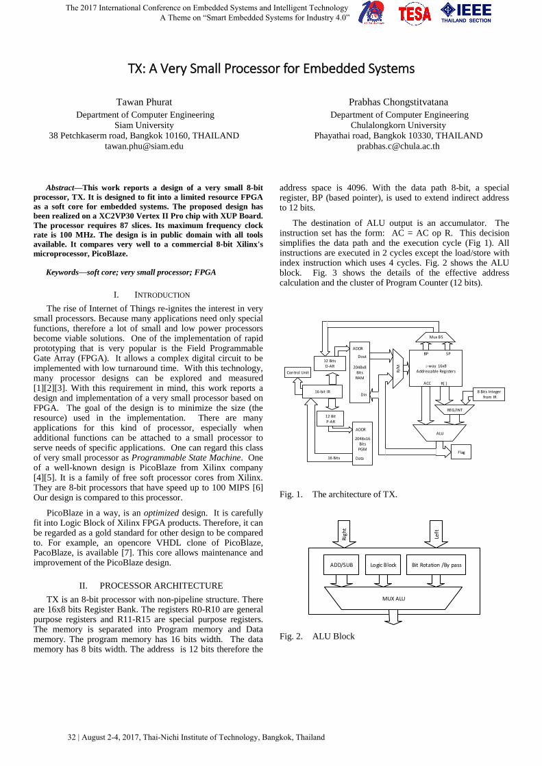
The destination of ALU output is an accumulator. The instruction set has the form: AC = AC op R. This decision simplifies the data path and the execution cycle (Fig 1). All instructions are executed in 2 cycles except the load/store with index instruction which uses 4 cycles. Fig. 2 shows the ALU block. Fig. 3 shows the details of the effective address calculation and the cluster of Program Counter (12 bits).
2048x8 Bits
RAM
16-bit IR
2-way 16x8 Addressable Registers
12 Bits D-AR
12 BitP-AR
16 Bits
Control Unit
Flag
ALU
ADDR
Dout
Din
2048x16 Bits
PGM
ADDR
Data
REG/INT
R/M
8 Bits Integer from IR
Mux BS
BP SP
ACC R[ ]
Fig. 1. The architecture of TX.
MUX ALU
ADD/SUB Logic Block Bit Rotation /By pass
Rig
ht
Left
Fig. 2. ALU Block
The 2017 International Conference on Embedded Systems and Intelligent Technology A Theme on “Smart Embedded Systems for Industry 4.0”
32 | August 2-4, 2017, Thai-Nichi Institute of Technology, Bangkok, Thailand

“1”
12-Bit D-AR
DAMux1
8 Bit BP
12 bits from IR
8 Bit ADDER
8 Bit R-Bus from RegBanks
12-Bit PC
PAMux1
CS
12 bits from IR
PAMux0
8 Bit R-Bus from RegBanks
PAMux2
ADDER
12 BIT ADDER
DS
Fig. 3. Data Address Register and Program Counter Cluster
III. INSTRUCTION SET
TX has 34 instructions. The instructions are grouped into 3 formats: L, R, and I (Long, Register, Immediate).
L op:4 ads:12
R op:4 xop:4 r1:4 r2:4
I op:4 xop:4 d:8
Where op denotes operation code, ads -- address,
xop – extended opcode, r1-r2 – register number,
d – displacement value.
The following is a full list of instructions.
lda ads ac = M[ads] L
sta ads M[ads] = ac L
jmp ads PC = ads L
jt ads if F!=0 PC = ads L
jf ads if F==0 PC = ads L
call ads save retads, PC=ads L
ret PC = retads R
lca #d ac = d I
ldx r2 ac = M[BP+R[r2]] R
stx r2 M[BP+R[r2]] = ac R
add r2 ac = ac + R[r2] R
sub r2 ac = ac - R[r2] R
and r2 ac = ac & R[r2] R
or r2 ac = ac | R[r2] R
xor r2 ac = ac ^ R[r2] R
addi #d ac = ac + d I
subi #d ac = ac - d I
andi #d ac = ac & d I
ori #d ac = ac | d I
xori #d ac = ac ^ d I
eq r2 F = ac == R[r2] R
lt r2 F = ac < R[r2] R
le r2 F = ac <= R[r2] R
gt r2 F = ac > R[r2] R
ge r2 F = ac >= R[r2] R
eqi #d F = ac == d I
lti #d F = ac < d I
lei #d F = ac <= d I
gti #d F = ac > d I
gei #d F = ac >= d I
mov r2 R[r2] = ac R
mva r2 ac = R[r2] R
not ac = ~ac R
clr r2 R[r2] = 0 R
The current implementation has only one level call/return and one level of interrupt. The indirect address is achieved with ldx/stx using BP to extend the address bit. The rest of instructions are straight forward. Here is an example of a simple program to sum all elements in an array. It shows how to access an array using index and some simple conditional jumps.
sum:
clr r1 ; clear index
clr r2 ; clear sum
lca #&ax ; set base address
mov bp ; move it to BP
loop:
lca #10 ; array size is 10
gt r1
jf exit ; while index < 10
ldx r1 ; ac = ax[i]
add r2
mov r2 ; keep sum in r2
jmp loop
exit: ; end of program
IV. IMPLEMENTATION
The design is realized using Verilog HDL in the environment of Xilinx ISE Foundation. The experiment is done on Vertex II Pro XUP board and interface with some additional interfaced circuits of seven segments LED and switches (Fig 4).
Fig. 4. Implementation of TX on XUP Vertex II Pro Board
The 2017 International Conference on Embedded Systems and Intelligent Technology A Theme on “Smart Embedded Systems for Industry 4.0”
33 | August 2-4, 2017, Thai-Nichi Institute of Technology, Bangkok, Thailand

Table I shows the resource utilization of TX. Table II shows the comparison between TX and PicoBlaze. TX instructions use two or four cycles while all instructions in PicoBlaze use two cycles.
TABLE I. RESOURCE UTILIZATION OF TX
Circuit Number of
Slices Slice F/F 4-LUTs
Carry Look Ahead Adder 10 0 18
Rotate Left/Right 8 0 16
Logic Function Block 4 0 8
Total ALU Block 10 0 18
Register Bank 16 16 30
DAR 15 0 27
PAR 15 0 27
CU 31 26 54
ALL CPU 87 58 156
TABLE II. COMPARE TX AND PICO BLAZE
Circuit Number of
Slices Slice F/F 4-LUTs
Pico Blaze (KCM3) 104 76 181
TX 87 58 156
V. DISCUSSION AND CONCLUSION
Compare to PicoBlaze, TX is smaller. The advantage of TX is that it is open source, therefore lends itself to be easy to modify and use in various applications. The behavioural simulation can be done easily. There are several opencore
processor designs that are available. For example, PacoBlaze [7], it is an opencore VHDL clone of PicoBlaze. This core allows maintenance and improvement of the PicoBlaze design. The aim of TX is similar. We have made available the HDL design and Assembler, Simulator tools for free public use [8].
TX has been designed to be an accumulator-based processor. However, its instruction set has a room for many additional instructions. For example, although the design presented here uses an accumulator, the instruction format allows two registers to be addressed in one instruction. Therefore the instruction such as "add r1 r2" (R[r1] = R[r1] + R[r2]) can be implemented easily. This can improved the code density as well as the performance of the processor.
REFERENCES
[1] Yunjie Zhang, Lei Bao, “The Design of an 8-Bit CISC CPU Based on FPGA,” International Conference on Wireless Communications Networking and Mobile Computing , 2011, pp. 1-4.
[2] Nachiket Kapre, “Custom FPGA-based soft-processors for sparse graph acceleration,” IEEE International Conference on Application-specific Systems, Architectures and Processors , 2015, pp. 9-16.
[3] Seema M. Borawake,and P. G. Chilveri, “Implementation of Wireless Sensor Network Using Microblaze and Picoblaze Processors,” International Conference on Communication Systems and Network Technologies, 2014, pp.1059 –1064.
[4] online (retrieve 10 June 2017): www .xilinx. com/ products/ intellectual-property/ picoblaze.html
[5] online (retrieve 10 June 017): www .xilinx. com/ support/ documentation/ ip_documentation/ug129.pdf
[6] online (retrieve 10 June 2017): en.wikipedia.org/wiki/PicoBlaze
[7] online (retrieve 10 June 2017): bleyer.org/pacoblaze/
[8] online (retrieve 10 June 2017): www. cp. eng. chula. ac. th/ ~piak/ project/tx/tx-v1.htm
The 2017 International Conference on Embedded Systems and Intelligent Technology A Theme on “Smart Embedded Systems for Industry 4.0”
34 | August 2-4, 2017, Thai-Nichi Institute of Technology, Bangkok, Thailand