Embed Size (px)
Citation preview

Two Way Radio Flash MCU
HT98F069
Revision: V1.10 Date: ovee 01ovee 01

Rev. 1.10 ovee 01 Rev. 1.10 3 ovee 01
HT98F069Two Way Radio Flash MCU
HT98F069Two Way Radio Flash MCU
Table of Contents
Features ............................................................................................................ 6Audio Pocesso Featues ....................................................................................................... CPU Featues ......................................................................................................................... 7
General Description ........................................................................................ 8Block Diagram .................................................................................................. 8Pin Assignment ................................................................................................ 9Pin Description ...............................................................................................11Absolute Maximum Ratings .......................................................................... 13D.C. Characteristics ....................................................................................... 13A.C. Characteristics ....................................................................................... 15LVR/LVD Electrical Characteristics .............................................................. 16A/D Converter Characteristics ...................................................................... 17D/A Converter Characteristics ...................................................................... 17Audio Processor Characteristics ................................................................. 18Power-on Reset Characteristics ................................................................... 19System Architecture ...................................................................................... 20
Clocking and Pipelining ......................................................................................................... 0Poga Counte – PC .......................................................................................................... 1Stack ..................................................................................................................................... Aithetic and Logic Unit – ALU ...........................................................................................
Flash Program Memory ................................................................................. 23Stuctue ................................................................................................................................ 3Special Vectos ..................................................................................................................... 3Look-up Tale ........................................................................................................................ 4Tale Poga Exaple ........................................................................................................ 4In Cicuit Pogaing – ICP ............................................................................................... On-Chip Deug Suppot – OCDS ......................................................................................... In Application Pogaing – IAP ........................................................................................
RAM Data Memory ......................................................................................... 34Stuctue ................................................................................................................................ 34Geneal Pupose Data Meoy ............................................................................................ 3Special Pupose Data Meoy ............................................................................................. 3

Rev. 1.10 ovee 01 Rev. 1.10 3 ovee 01
HT98F069Two Way Radio Flash MCU
HT98F069Two Way Radio Flash MCU
Special Function Registers ........................................................................... 37Indiect Addessing Registes – IAR0 IAR1 ......................................................................... 37Meoy Pointes – MP0 MP1 .............................................................................................. 37Bank Pointe – BP ................................................................................................................. 38Accuulato – ACC ............................................................................................................... 38Poga Counte Low Registe – PCL .................................................................................. 38Look-up Tale Registes – TBLP TBHP TBLH ..................................................................... 39Status Registe – STATUS .................................................................................................... 39Syste Contol Registes – CTRL0 CTRL1 CTRL ........................................................... 40
Oscillators ...................................................................................................... 43Syste Oscillato Oveview .................................................................................................. 43Intenal PLL Fequency Geneato ........................................................................................ 43Extenal 378Hz Cystal Oscillato – LXT ........................................................................... 43Intenal 3kHz Oscillato – LIRC ........................................................................................... 4
Operating Modes .......................................................................................... 45Mode Types and Selection .................................................................................................... 4Mode Switching ..................................................................................................................... 48Standy Cuent Consideations ........................................................................................... 48Wake-up ................................................................................................................................ 49
Watchdog Timer ............................................................................................. 50Watchdog Tie Clock Souce .............................................................................................. 0Watchdog Tie Contol Registes ....................................................................................... 0Watchdog Tie Opeation ................................................................................................... 1
Reset and Initialisation .................................................................................. 52Reset Functions .................................................................................................................... Reset Initial Conditions .........................................................................................................
Input/Output Ports ......................................................................................... 58Pull-high Resistos ................................................................................................................ 9Pot A Wake-up ..................................................................................................................... 9I/O Pot Contol Registes ..................................................................................................... 9Pin-shaed Functions ............................................................................................................ 0Pin Remapping Configuration ............................................................................................... 1I/O Pin Stuctue .................................................................................................................... Pogaing Consideations ................................................................................................

Rev. 1.10 4 ovee 01 Rev. 1.10 ovee 01
HT98F069Two Way Radio Flash MCU
HT98F069Two Way Radio Flash MCU
Timer/Event Counters ................................................................................... 63Configuring the Timer/Event Counter Input Clock Source .................................................... 3Tie Registes – TMR0 TMR1 TMRL TMRH ............................................................... 4Tie Contol Registes – TMR0C TMR1C TMRC ........................................................... Tie Mode ........................................................................................................................... 7Event Counte Mode ............................................................................................................. 7Pulse Width Captue Mode ................................................................................................... 8Pescale ............................................................................................................................... 9PFD Function ........................................................................................................................ 9I/O Intefacing ........................................................................................................................ 70Pogaing Consideations ................................................................................................ 70Tie Poga Exaple ....................................................................................................... 71Tie Base ............................................................................................................................. 71
Analog to Digital Converter ......................................................................... 72A/D Oveview ........................................................................................................................ 7A/D Convete Data Registes – ADRL ADRH ..................................................................... 7A/D Convete Contol Registes – ADCR ACSR ACSR .................................................. 73A/D Opeation ....................................................................................................................... 7A/D Input Pins ....................................................................................................................... 7Suay of A/D Convesion Steps ....................................................................................... 7Pogaing Consideations ................................................................................................ 77A/D Tansfe Function ........................................................................................................... 77A/D Pogaing Exaple ................................................................................................... 78
Interrupts ........................................................................................................ 80Inteupt Registe .................................................................................................................. 80Inteupt Opeation ................................................................................................................ 8Inteupt Pioity ..................................................................................................................... 83Extenal Inteupt ................................................................................................................... 84Tie/Event Counte Inteupt ............................................................................................... 84A/D Convete Inteupt ......................................................................................................... 84Tie Base Inteupt ............................................................................................................... 8Audio Pocesso Inteupt ..................................................................................................... 8Inteupt Wake-up Function ................................................................................................... 8Pogaing Consideations ................................................................................................ 8
Low Voltage Detector – LVD ......................................................................... 86LVD Registe ......................................................................................................................... 8LVD Opeation ....................................................................................................................... 87
SPI Function ................................................................................................... 88BEEP Function ............................................................................................... 89Digital to Analog Converter – DAC ............................................................... 89
Opeation .............................................................................................................................. 89

Rev. 1.10 4 ovee 01 Rev. 1.10 ovee 01
HT98F069Two Way Radio Flash MCU
HT98F069Two Way Radio Flash MCU
Audio Processor ............................................................................................ 91Audio Receive ...................................................................................................................... 91Audio Tansitte .................................................................................................................. 93Suppoted Diffeent Coination Functions ......................................................................... 9
Audio Signal Routing .................................................................................... 97MCU Interfacing ............................................................................................. 98
Coand Goups ................................................................................................................. 98I/O Coand Goup Suay ......................................................................................... 101I/O Coand Goup Detail ................................................................................................. 10CLI Coand Goup Suay .......................................................................................... 108CLI Coand Goup Detail .................................................................................................110
Configuration Options ..................................................................................118Application Circuits ......................................................................................119Instruction Set .............................................................................................. 120
Intoduction ......................................................................................................................... 10Instuction Tiing ................................................................................................................ 10Moving and Tansfeing Data ............................................................................................. 10Aithetic Opeations .......................................................................................................... 10Logical and Rotate Opeation ............................................................................................. 11Banches and Contol Tansfe ........................................................................................... 11Bit Opeations ..................................................................................................................... 11Tale Read Opeations ....................................................................................................... 11Othe Opeations ................................................................................................................. 11
Instruction Set Summary ............................................................................ 122Tale Conventions ............................................................................................................... 1
Instruction Definition ................................................................................... 124Package Information ................................................................................... 133
48-pin LQFP (7×7) Outline Diensions .................................................................. 1344-pin LQFP (7×7) Outline Diensions .................................................................. 13

Rev. 1.10 ovee 01 Rev. 1.10 7 ovee 01
HT98F069Two Way Radio Flash MCU
HT98F069Two Way Radio Flash MCU
Features
Audio Processor Features• AudioProcessorworkingfrequencyupto24.576MHz
• Operatingvoltage:3.3V~5.5V
• PGA:5-bitOperationalAmplifierGainsetup
• ProgrammableAudioScrambler
• Sub-toneprocessor♦ User-definedCTCSS/DCSencoder/decoder
• In-band-toneprocessor♦ DTMFencoder/decoder♦ Selectivecallencoder/decoder♦ User-definedtoneencoder/decoder
• Audio-bandProcessing♦ Pre-emphasis/de-emphasis♦ Scrambler♦ Compandor♦ VOX
• SPIInterfaceforexternalMCUcontrol
• TXOutputforSingle-PointModulation
Audio and SuAudio Pocesso
Holtek8-it MCU
ExtenalMCU
SPI BUS & SPI IT
Modulato
Deodulato
RFBlock
HT98F069
Note:ThisintegratedAudioProcessorcanbecontrolledbyeithertheinternalMCUoranexternalMCU.
Audio Processor

Rev. 1.10 ovee 01 Rev. 1.10 7 ovee 01
HT98F069Two Way Radio Flash MCU
HT98F069Two Way Radio Flash MCU
CPU Features• Operatingvoltage:
♦ fSYS=32768Hz:2.2V~5.5V♦ fSYS=4.096MHz:2.2V~5.5V♦ fSYS=8.192MHz:2.2V~5.5V♦ fSYS=12.288MHz:3.3V~5.5V♦ fSYS=16.384MHz:3.3V~5.5V
• Upto0.24μsinstructioncyclewith16.384MHzsystemclockatVDD=5V
• Powerdownandwake-upfunctionstoreducepowerconsumption
• Multi-modeoperation:Normal,Slow,IdleandSleep
• Oscillatortypes:♦ External32768Hzlowspeedcrystal–LXT♦ Internal32kHzlowspeedRC–LIRC
• InternalPLLtogeneratethesystemclock♦ Inputreferenceclock:32768Hz♦ Output:2.048MHz×12/×16/×20/×24(optional)
• Allinstructionsexecutedinoneortwoinstructioncycles
• Tablereadinstruction
• 63powerfulinstructions
• 10-levelsubroutinenesting
• Bitmanipulationinstruction
• FlashProgramMemory:24K×16
• RAMDataMemory:1152×8
• WatchdogTimerfunction
• Upto42bidirectionalI/Olines
• OneexternalinterruptpinsharedwithI/Opin
• 8-channel12-bitA/DConverter
• 4-channel8-bitD/AConverter
• Two8-bitandone16-bitprogrammableTimer/EventCounterswithoverflowinterruptandprescaler
• ProgrammableFrequencyDivider–PFD
• SingleTime-Basefunctionforgenerationoffixedtimeinterruptsignals
• Lowvoltagereset/detectfunction
• Flashprogrammemorycanbere-programmedupto1,000,000times
• Flashprogrammemorydataretention>10years
• Packagetypes:48-pinLQFP,64-pinLQFP

Rev. 1.10 8 ovee 01 Rev. 1.10 9 ovee 01
HT98F069Two Way Radio Flash MCU
HT98F069Two Way Radio Flash MCU
General Description TheHT98F069deviceisaFlashASSPMCUforanalogtwowayradioapplicationssuchasFRS.Itcontainsan8-bitMCU,anAudioProcessor,a16-bitdelta-sigmaA/Dconverter, two16-bitD/Aconvertersandanoperationalamplifierforperipheral interfaces.It includesan8-channel12-bitA/Dconverter,a4-channel8-bitD/Aconverter,anLXToscillatorfunction,anexternalinterrupt,24KwordsofFlashProgramMemoryand1152bytesofSRAMDataMemoryforgeneralMCUcontrolapplication.TheintegratedAudioProcessorcanbeaccessedbytheMCUusing its internalSPIinterface.TheInternalAudioProcessorsupportsvariousprogrammablefunctions.ThesefunctionsincludeaCTCSS/DCSencoder/decoder,DTMFencoder/decoder,scramble/descramble,VOXandcompandor,etc.ByconnectingtoasuitableRFmodule, thisdeviceprovidesacosteffectiveandextremelyflexibleFRSsolution.Applicationswillincludeproductsintheleisureradioapplicationareasuchasgeneralmobileradios,personalmobileradiosandmultipleuserradios.
Block Diagram
Overall Block Diagram
8-bit MCU
MIC_I
MIC_O
VAG
AUDO
SMOD
AUX
BEEP1
DEMOD
Sub Audio TX
Sub Audio RX
MODO
DAC BIAS
SPII/O ConfigCLI Config
SPI us & SPI IT (fo use MCU)
PLLOSCMeasue
Rende
I/O
XI
XOUT
InbandSignaling
LPF70
HPF300
ARROW/WIDE BAD DEEMPHASIS EXPADER DESCRAMBLE
TX/RXMode
Control
ARROW/WIDE BAD SCRAMBLE COMPRESSOR EMPHASISHPF300
AMP
AMP1OPA PGA
DAC
DAC1ADC
Inband Decoders
Selecte Call Decode
DTMFDecode
Use Tone Decode
Tone SquelchDecoders
DCS Decode
CTCSSDecode
BUF
VR1
Use Tone Geneato
DTMF Geneato
Selective CallGeneato
Tone SquelchSignaling
VR
DCS & DCS OFF TOE
Geneato
CTCSS & CTCSS OFF TOEGeneato
DAC
ADC
Audio Processing
Audio Processing

Rev. 1.10 8 ovee 01 Rev. 1.10 9 ovee 01
HT98F069Two Way Radio Flash MCU
HT98F069Two Way Radio Flash MCU
Internal 8-Bit MCU Block Diagram
8-itRISCMCUCoe
IAPFlash
PogaMeoy
FlashPogaing
Cicuity
RAMData
Meoy
LowVoltageDetect
WatchdogTie
InteuptContolle
ResetCicuit
LXT
1-it A/DConvete
PFD Dive
8-it D/A Convete
LowVoltageReset
PLL
I/O
Tie Base
SPI Tie/Event Countes
Pin Assignment
DEMOD
VAGREF
PE0
PB
0/DA
O0
VSSA2VCCA2 PB6/GPIO2
XOU
T
MIC
_I
PC
6/SPIC
KPC
7/SPISSPD
0
VSS
A1
MIC
_O
PD1
PA
6/TMR
2P
A5/MIS
OP
A4/TM
R1
PC
4/MO
SIP
C5/S
PIRQ
PA3/AN3/INTPA2/AN2/TMR0/ICPCK/OCDSCKPA1/AN1/PFDPA0/AN0/ICPDA/OCDSDAPB7/GPIO3
PA7/RESPC3/AN7
PC0/AN4
PC2/AN6PC1/AN5
VS
S
VDD
XINP
LLCP
B5/G
PIO
1P
B4/G
PIO
0PD
3PD
2P
B3/D
AO
3P
B2/D
AO
2P
B1/D
AO
1
VAG
AUDOMODO
VCCA1AUX
SMOD
PE1 HT98F069/HT98V06948 LQFP-A
123456789101112
13 14 15 16 17 18 19 20 21 22 23 24252627282930313233343536
45464748 3738394041424344

Rev. 1.10 10 ovee 01 Rev. 1.10 11 ovee 01
HT98F069Two Way Radio Flash MCU
HT98F069Two Way Radio Flash MCU
PD4
PF6PA7/R
ES
VDD
PF1PF2
PF5PF4
PF3
PD5
PD7PD6
HT98F069/HT98V06964 LQFP-A
12345678910111213
20 21 22 23 24 25 26 27 28
6061626364
29 30 31 32
5253545556575859
141516
434445464748
36373839404142
333435
17 18 19
495051DEMOD
VAGREF
PE0
VSSA2VCCA2
VAG
AUDOMODO
VCCA1AUX
SMOD
PE1
PB2/DAO2PB1/DAO1PB0/DAO0
PF0
XOU
TVS
SA
XINPLLCPB
5/GP
IO1
PB4/G
PIO
0PD
3PD
2PB
3/DA
O3
VSS
VCC
A4
VCC
A3
PA3/AN3/INTPA2/AN2/TMR0/ICPCK/OCDSCKPA1/AN1/PFDPA0/AN0/ICPDA/OCDSDAPB7/GPIO3
PC3/AN7
PC0/AN4
PC2/AN6PC1/AN5
PB6/GPIO2
MIC
_I
PC6/SPIC
KPC
7/SPISSPD
0
PF7M
IC_O
PD1
PA6/TM
R2
PA
5/MIS
OPA
4/TMR
1PC
4/MO
SI
PC5/SPIR
Q
VSS
VS
SA1
Note:1.Ifthepin-sharedpinfunctionshavemultipleoutputssimultaneously,itspinnamesattherightsideofthe"/"signcanbeusedforhigherpriority.
2.TheINT,TMR0andPFGpinfunctionscanberemappedtootherpinscontrolledbythesamecontrolbit.RefertotheCTRL0registerintheSystemControlRegisterssection.

Rev. 1.10 10 ovee 01 Rev. 1.10 11 ovee 01
HT98F069Two Way Radio Flash MCU
HT98F069Two Way Radio Flash MCU
Pin DescriptionAsthePinDescriptiontableshowsthesituationforthepackagewiththemostpins,notallpinsinthetablewillbeavailableonsmallerpackagesizes.
Pad Name Function OPT I/T O/T Description
PA0/A0/ICPDA/OCDSDA
PA0 PAPUPAWK ST CMOS Geneal pupose I/O. Registe enaled pull-up and wake-up.
A0 ACSR A — A/D convete analog input 0ICPDA — — — ICP Seial Data/Addess pin
OCDSDA — — — OCDS Data/Addess pin fo EV chip only.
PA1/A1/PFDPA1 PAPU
PAWK ST CMOS Geneal pupose I/O. Registe enaled pull-up and wake-up.
A1 ACSR A — A/D convete analog input 1PFD CTRL0 — CMOS PFD output
PA/A/TMR0/ICPCK/OCDSCK
PA PAPUPAWK ST CMOS Geneal pupose I/O. Registe enaled pull-up and wake-up
A ACSR A — A/D convete analog input
TMR0 CTRL0TMR0C ST — Tie/Event Counte 0 clock input
ICPCK — — — ICP Clock pinOCDSCK — — — OCDS Clock pin fo EV chip only.
PA3/A3/IT
PA3 PAPUPAWK ST CMOS Geneal pupose I/O. Registe enaled pull-up and wake-up.
A3 ACSR A — A/D convete analog input 3
ITCTRL0CTRL1ITC0
ST — Extenal inteupt input
PA4/TMR1PA4 PAPU
PAWK ST CMOS Geneal pupose I/O. Registe enaled pull-up and wake-up.
TMR1 TMR1C ST — Tie/Event Counte 1 clock input
PA/MISOPA PAPU
PAWK ST CMOS Geneal pupose I/O. Registe enaled pull-up and wake-up.
MISO SPICR — — Slave SPI output data pin
PA/TMRPA PAPU
PAWK ST CMOS Geneal pupose I/O. Registe enaled pull-up and wake-up.
TMR TMRC ST — Tie/Event Counte clock input
PA7/RESPA7 PAWK ST MOS Geneal pupose I/O. Registe enaled wake-up.RES CO ST — Extenal eset pin
PB0/DAO0PB0 PBPU ST CMOS Geneal pupose I/O. Registe enaled pull-up.
DAO0 DACR — A DAC0 output
PB1/DAO1PB1 PBPU ST CMOS Geneal pupose I/O. Registe enaled pull-up.
DAO1 DACR — A DAC1 output
PB/DAOPB PBPU ST CMOS Geneal pupose I/O. Registe enaled pull-up.
DAO DACR — A DAC output
PB3/DAO3PB3 PBPU ST CMOS Geneal pupose I/O. Registe enaled pull-up.
DAO3 DACR — A DAC3 output
PB4/GPIO0PB4 PBPU ST CMOS Geneal pupose I/O. Registe enaled pull-up.
GPIO0 SPICR — — Audio pocesso I/O 0
PB/GPIO1PB PBPU ST CMOS Geneal pupose I/O. Registe enaled pull-up.
GPIO1 SPICR — — Audio Pocesso I/O 1
PB/GPIOPB PBPU ST CMOS Geneal pupose I/O. Registe enaled pull-up.
GPIO SPICR — — Audio Pocesso I/O

Rev. 1.10 1 ovee 01 Rev. 1.10 13 ovee 01
HT98F069Two Way Radio Flash MCU
HT98F069Two Way Radio Flash MCU
Pad Name Function OPT I/T O/T Description
PB7/GPIO3PC0 PCPU ST CMOS Geneal pupose I/O. Registe enaled pull-up.
GPIO3 SPICR — — Audio Pocesso I/O 3PC0/A4PC1/APC/APC3/A7
PCn PCPU ST CMOS Geneal pupose I/O. Registe enaled pull-up.
An ADCSR A — A/D convete analog input 4 7
PC4/MOSIPC4 PCPU ST CMOS Geneal pupose I/O. Registe enaled pull-up.
MOSI SPICR — — Slave SPI input data pin
PC/SPIRQPC PCPU ST CMOS Geneal pupose I/O. Registe enaled pull-up.
SPIRQ SPICR — — Slave SPI output pin
PC/SPICKPC PCPU ST CMOS Geneal pupose I/O. Registe enaled pull-up.
SPICK SPICR — — Slave SPI clock souce input pin
PC7/SPISSPC7 PCPU ST CMOS Geneal pupose I/O. Registe enaled pull-up.
SPISS SPICR — — Audio Pocesso select pinPD0~PD7 PDn PDPU ST CMOS Geneal pupose I/O. Registe enaled pull-up.PE0~PE1 PEn PEPU ST CMOS Geneal pupose I/O. Registe enaled pull-up.PF0~PF7 PFn PFPU ST CMOS Geneal pupose I/O. Registe enaled pull-up.XI XI — LXT — Low fequency cystal input pinXOUT XOUT — — LXT Low fequency cystal output pinMIC_I MIC_I — — — Micophone OP inputMIC_O MIC_O — — — Micophone OP outputAUX AUX — — — Auxiliay audio input AUDO AUDO — — — Audio outputMODO MODO — — — Audio aseand odulation output to RF oduleSMOD SMOD — — — Su-tone aseand odulation outputDEMOD DEMOD — — — PGA Input fo RF deodulation outputVCCA1 VCCA1 — — — Analog Block VCC VSSA1 VSSA1 — — — Analog Block GD VCCA VCCA — — — Analog Block VCC VSSA VSSA — — — Analog Block GD VAG VAG — — — Audio ADC analog gound outputVAGREF VAGREF — — — Audio ADC analog gound efeence ypassPLLC PLLC — — — Connect to low pass loop filter circuitVDD VDD — PWR — Positive powe supplyVSS VSS — PWR — egative powe supply GD
Legend:I/T:Inputtype; O/T:Outputtype; OPT:Optionalbyconfigurationoption(CO)orregisteroption; PWR:Power; CO:Configurationoption ST:SchmittTriggerinput; AN:Analogsignal; CMOS:CMOSoutput; NMOS:NMOSoutput LXT:Lowfrequencycrystaloscillator

Rev. 1.10 1 ovee 01 Rev. 1.10 13 ovee 01
HT98F069Two Way Radio Flash MCU
HT98F069Two Way Radio Flash MCU
Absolute Maximum RatingsSupplyVoltage................................................................................................VSS−0.3VtoVSS+6.0VInputVoltage..................................................................................................VSS−0.3VtoVDD+0.3VStorageTemperature....................................................................................................-50˚Cto125˚COperatingTemperature..................................................................................................-40˚Cto85˚CIOLTotal..................................................................................................................................... 80mAIOHTotal....................................................................................................................................-80mATotalPowerDissipation......................................................................................................... 500mW
Note:Theseare stress ratingsonly.Stresses exceeding the range specifiedunder "AbsoluteMaximumRatings"maycausesubstantialdamagetothedevice.Functionaloperationofthisdeviceatotherconditionsbeyondthoselistedinthespecificationisnotimpliedandprolongedexposuretoextremeconditionsmayaffectdevicereliability.
D.C. CharacteristicsTa=°C
Symbol ParameterTest Conditions
Min. Typ. Max. UnitVDD Conditions
VDD MCU Opeating Voltage
— fSYS=378Hz . — .
V— fSYS=4.09MHz . — .— fSYS=8.19MHz . — .— fSYS=1.88MHz 3.3 — .— fSYS=1.384MHz 3.3 — .
IDD
Opeating Cuent(LXT+PLL)
3V o load fSYS=4.09MHz ADC disale DAC disale Audio Pocesso off
— 4A
V — 4 8
Opeating Cuent(LXT+PLL)
3V o load fSYS=8.19MHz ADC disale DAC disale Audio Pocesso off
— 4A
V — 4 8
Opeating Cuent(LXT+PLL)
3.3V o load fSYS=1.88MHz ADC disale DAC disale Audio Pocesso off
— 4A
V — 4 8
Opeating Cuent(LXT+PLL)
3.3V o load fSYS=1.384MHz ADC disale DAC disale Audio Pocesso off
— 4 1A
V — 1
Opeating Cuent(LXT on PLL off)
3V o load fSYS=378Hz ADC disale DAC disale Audio Pocesso off
— 0 30μA
V — 40 0
Opeating Cuent(Audio Pocesso on) 3.3V o load fAP=4.7MHz (ote) — — A
ISTB
Standy Cuent(LIRC off LXT offPLL off: PLLE=0&CLKMOD=1)
3V o load MCU poweed down
— — 1μA
V — —
Standy Cuent(LIRC on LXT offPLL off: PLLE=0&CLKMOD=1)
3V o load MCU poweed down
— — μA
V — — 10
Standy Cuent(LIRC off LXT onPLL off: PLLE=0&CLKMOD=1)
3V o load MCU poweed downLXT slowly stat-up
— — μA
V — — 10
VILInput Low Voltage fo I/O Pots — — 0 — 0.3VDD VInput Low Voltage fo RES pin — — 0 — 0.4VDD V

Rev. 1.10 14 ovee 01 Rev. 1.10 1 ovee 01
HT98F069Two Way Radio Flash MCU
HT98F069Two Way Radio Flash MCU
Symbol ParameterTest Conditions
Min. Typ. Max. UnitVDD Conditions
VIHInput High Voltage fo I/O Pots — — 0.7VDD — VDD VInput High Voltage fo RES pin — — 0.9VDD — VDD V
IOH I/O Souce Cuent 3V
VOH=0.9VDD- -4 —
AV - -10 —
IOL I/O Sink Cuent 3V
VOL=0.1VDD4 8 —
AV 10 0 —
RPH Pull-high Resistance fo I/O Pots3V
—0 0 100
kΩV 10 30 0
VDEMOD DEMOD Input Voltage Range 3.3V PGA Gain=0dB — — ±1100 VVMIC MIC Input Voltage Range 3.3V PGA Gain=0dB — — ±1100 VVAUX AUX Input Voltage Range 3.3V PGA Gain=0dB — — ±1100 VVAUDO AUDO Output Voltage Range 3V o load 0.01 — 0.99 VDD
VMODO MODO Output Voltage Range 3V o load 1/4 — 3/4 VDD
VSMOD SMOD Output Voltage Range 3V o load 1/4 — 3/4 VDD
IAUDOH AUDO Souce Cuent 3V VOH=0.9VDD — -4 — AIAUDOL AUDO Sink Cuent 3V VOL=0.1VDD — 8 — A
RAUX_OAUX Input Resistance When Channel Tun On — — — 300 — Ω
RAUX_OFFAUX Input Resistance When Channel Tun Off — — 1 — — MΩ
RDEMOD_ODEMOD Input Resistance When MUX Channel Tun On — — — 300 — kΩ
RDEMOD_OFFDEMOD Input Resistance When MUX Channel Tun Off — — 1 — — MΩ
RMODO_OMODO Output Resistance When DAO1 OPA Tun On — — — 300 — Ω
RMODO_OFFMODO Output Resistance When DAO1 OPA Tun Off — — — 00 — kΩ
RSMOD_OSMOD Output Resistance When DAO OPA Tun On — — — 300 — Ω
RSMOD_OFFSMOD Output Resistance When DAO OPA Tun Off — — — 00 — kΩ
RLLoad Resistance fo MODO and SMOD — — 0 — — kΩ
VAG Audio ADC analog gound output — — -% VDD/ +% V
Note:1.EachofthePA0~PA6pinsisconnectedtoanexternalpull-upresistorwhentheRESpinislow.2.TheADCandDACin theMCU,AudioScrambler,CTCSS,DCS,compandorandpre-emphasis/de-emphasisaredisabled,whileall theotherdigitalcircuitsincludingthemainclockPLLareenabled.Asingleanalogpathisenabledthroughthedevice.

Rev. 1.10 14 ovee 01 Rev. 1.10 1 ovee 01
HT98F069Two Way Radio Flash MCU
HT98F069Two Way Radio Flash MCU
A.C. CharacteristicsTa=°C
Symbol ParameterTest Conditions
Min. Typ. Max. UnitVDD Conditions
fPLL PLL Clock 3.3V~.V
M[1:0]=00
-1%
4.7
+1% MHzM[1:0]=01 3.78
M[1:0]=10 40.90
M[1:0]=11 49.1
fSYS Syste Clock (LXT) — — — 378 — Hz
fTIMER Tie Input Fequency (TMRn)
.V~.V — 0 — 4
MHz3.3V~.V — 0 — 8
4.V~.V — 0 — 1
fLIRC Low Speed RC Oscillato Clock
V Ta=°C -10% 3 +10%
kHzV±0.V Ta= -40°C~8°C -40% 3 +40%
.V~.V Ta= -40°C~8°C -0% 3 +0%
tRES
MCU Extenal Reset Low Pulse Width — — 10 — — μs
Audio Pocesso Reset (AUPRST) Low Pulse Width — — 1 — — μs
tSST1
MCU Syste Stat-up Tie Peiod (Powe On Reset o Wake-up fo Powe Down Mode)
— MCU fSYS=378Hz -10% 104 — tSYS
tSSTAudio Pocesso Syste Stat-up Tie Peiod (Wake-up fo Reset) — — 100 — — s
tIT Inteupt Pulse Width — — 1 — — μs
tFUP
PLL Settling Tie (378Hz to 4.7/3.78/40.9/49.1MHz PLL Fequency Deviation < ±0.1%)
3.3VLXT on PLL off→on — — 10 s
V
tRSTD
Syste Reset Delay Tie(Powe On Reset LVR Hadwae Reset LVRC/WDTC Softwae Reset)
— — 0 100 s
Syste Reset Delay Tie(RES pin eset WDT hadwae eset IAP eset)
— — 8.3 1.7 33.3 s
Note:1.tSYS=1/fSYS2.M[1:0]arePLLCRregisterbit1andbit0.

Rev. 1.10 1 ovee 01 Rev. 1.10 17 ovee 01
HT98F069Two Way Radio Flash MCU
HT98F069Two Way Radio Flash MCU
LVR/LVD Electrical CharacteristicsTa=°C
Symbol ParameterTest Conditions
Min. Typ. Max. UnitVDD Conditions
VLVR Low Voltage Reset Voltage
— LVR enale voltage select .1V
-%
.1
+% V— LVR enale voltage select .V .
— LVR enale voltage select 3.1V 3.1
— LVR enale voltage select 3.8V 3.8
VLVDLow Voltage Detection Voltage
— LVD enale voltage select .0V
-%
.0
+% V
— LVD enale voltage select .V .
— LVD enale voltage select .4V .4
— LVD enale voltage select .7V .7
— LVD enale voltage select 3.0V 3.0
— LVD enale voltage select 3.3V 3.3
— LVD enale voltage select 3.V 3.
— LVD enale voltage select 4.0V 4.0
tLVR Low Voltage Width to Reset — — 10 40 480 μs
tLVDS LVDO Stale Tie— LVR enale LVD off → on — — 1 μs
— LVR disale LVD off → on — — 10 μs

Rev. 1.10 1 ovee 01 Rev. 1.10 17 ovee 01
HT98F069Two Way Radio Flash MCU
HT98F069Two Way Radio Flash MCU
A/D Converter CharacteristicsTa=°C
Symbol ParameterTest Conditions
Min. Typ. Max. UnitVDD Conditions
AVDD Opeating Voltage — VREF=AVDD .7 .0 . VVAD A/D Convete Input Voltage — VREF=AVDD 0 — AVDD V
DL A/D Diffeential on-lineaity
3V VREF=AVDD=VDD
tAD=0.μs-3 — +3 LSB
V3V VREF=AVDD=VDD
tAD=10μsV
IL A/D Integal on-lineaity
3V VREF=AVDD=VDD
tAD=0.μs-4 — +4 LSB
V3V VREF=AVDD=VDD
tAD=10μsV
IADCOpeating Cuent (only A/D enale othes disale)
3Vo load (tAD=0.5μs)
— 1.0 .0A
V — 1. 3.0tAD A/D Convete Clock Peiod .7V~.V — 0. — 10 μs
tADCA/D Convesion Tie (Include Saple and Hold Tie) .7V~.V — — 1 — tAD
tADS A/D Sapling Tie .7V~.V — — 4 — tAD
tOST A/D Convete On-to-Stat Tie .7V~.V — — — μs
Note:A/Dconversiontime(tADC)=n(bitsA/D)+4(samplingtime),theconversionforeachbitneedsoneA/Dclock(tAD).
D/A Converter CharacteristicsTa=°C
Symbol ParameterTest Conditions
Min. Typ. Max. UnitVDD Conditions
AVDD Opeating Voltage — — .7 .0 . V
DL D/A Diffeential on-lineaity V VREF=AVDD=VDD -0. — +0. LSB
IL D/A Integal non-lineaity V VREF=AVDD=VDD -1 — +1 LSB
IDAC Opeating Cuent 3V
o load VREF=AVDD=VDD— 300 —
μAV — 300 —
RO RR Output Resistance V — — 10 — kΩ

Rev. 1.10 18 ovee 01 Rev. 1.10 19 ovee 01
HT98F069Two Way Radio Flash MCU
HT98F069Two Way Radio Flash MCU
Audio Processor CharacteristicsOpeating Tepeatue: -40°C~8°C Ta=°C VDD=3.3V
Input stage gain=0dB. Output stage attenuation=0dBLXT fequency=378Hz ± 0.01% (100pp) fSYS dift < ±0.1%
Refeence signal level is 300Vs at 1kHz with VDD=3.3V
Symbol ParameterTest Conditions
Min. Typ. Max. UnitVDD Conditions
CTSS Receiver
Sensitivity (Pue Tone) 3.3V — — 0 — VP-P
Response Tie 3.3V — — 10 — s
De-esponse Tie 3.3V — — DT1+14 — s
DT1 Dopout Iunity 3.3V — 0 300 819 s
Fequency Range 3.3V — 0 — 0 Hz
DCS Receiver
Sensitivity 3.3V — 0 — — VP-P
Response Tie 3.3V — — 10 — s
De-esponse Tie 3.3V — — DT+10 — s
DT Dopout Iunity 3.3V — 0 — 819 s
Selective Call / User Tone & Audio Tone Receiver
Sensitivity (Pue Tone) 3.3V — — 1 — Vs
Response Tie 3.3V — — 3 — s
De-esponse Tie 3.3V — — 30 — s
Dopout Iunity 3.3V — — — s
Fequency Range 3.3V — 400 — 3000 Hz
DTMF Receiver
Sensitivity 3.3V — — — Vs
Response Tie 3.3V — — 3 — s
De-esponse Tie 3.3V — — 3 — s
Fequency Toleance 3.3V — — ±. — %
Fequency Rejection 3.3V — — ±3. — %
Audio Compandor
Attack Tie 3.3V — — 4 — s
Decay Tie 3.3V — — 14 — s
0dB Point 3.3V — — 100 — Vs
Copession/Expansion Ratio 3.3V — — :1 —
CTCSS Generator
Fequency Range 3.3V — 0 — 0 Hz
Fequency Accuacy 3.3V — — — ±0.3 %
Aplitude Toleance — — -1.0 0 +1.0 dB
Haonic Distotion — — — .0 4.0 %
Audio Channel Filter
Received Audio HPF 3.3V — 300 — 3400 Hz
1.kHz Channel Tansitted Audio 3.3V — 300 — 0 Hz
kHz Channel Tansitted Audio 3.3V — 300 — 3000 Hz

Rev. 1.10 18 ovee 01 Rev. 1.10 19 ovee 01
HT98F069Two Way Radio Flash MCU
HT98F069Two Way Radio Flash MCU
Symbol ParameterTest Conditions
Min. Typ. Max. UnitVDD Conditions
Pass-and Gain 3.3V Fequency=1.0kHz — 0 — dB
Pass-and Ripple 3.3V Fequency=1.0kHz -.0 0 +0. dB
Stop-and Attenuation 3.3V
Fo 1.kHz channel stop and at 3.4kHz;Fo kHz channel stop and at 3.7kHz;
30 — — dB
Residual Hu and oise 3.3V — — -0 — dB
De-ephasis 3.3V — — + — dB/oc
Pe-ephasis 3.3V — — - — dB/oc
Audio Scrambler
Invesion Fequency 3.3V — — 3300 — Hz
Pass Band 3.3V — 300 — 3000 Hz
Audio Expandor
Input Signal Range 3.3V — — 300 — Vs
Power-on Reset CharacteristicsTa=°C
Symbol ParameterTest Conditions
Min. Typ. Max. UnitVDD Conditions
VPOR VDD Stat Voltage to Ensue Powe-on Reset — — — — 100 V
RRPOR VDD Rising Rate to Ensue Powe-on Reset — — 0.03 — — V/s
tPORMiniu Tie fo VDD Stays at VPOR to Ensue Powe-on Reset — — 1 — — s
VDD
tPOR RRPOR
VPOR
Tie

Rev. 1.10 0 ovee 01 Rev. 1.10 1 ovee 01
HT98F069Two Way Radio Flash MCU
HT98F069Two Way Radio Flash MCU
System ArchitectureAkeyfactorinthehigh-performancefeaturesoftheHoltekrangeofmicrocontrollersisattributedtotheinternalsystemarchitecture.TherangeofdevicetakeadvantageoftheusualfeaturesfoundwithinRISCmicrocontrollersprovidingincreasedspeedofoperationandenhancedperformance.Thepipeliningscheme is implemented insuchaway that instruction fetchingand instructionexecutionareoverlapped,hence instructionsareeffectivelyexecuted inonecycle,with theexceptionofbranchorcall instructions.An8-bitwideALUisusedinpracticallyalloperationsof the instructionset. Itcarriesoutarithmeticoperations, logicoperations, rotation, increment,decrement,branchdecisions,etc.TheinternaldatapathissimplifiedbymovingdatathroughtheAccumulatorandtheALU.Certain internal registersare implemented in theDataMemoryandcanbedirectlyor indirectlyaddressed.Thesimpleaddressingmethodsof theseregistersalongwithadditionalarchitecturalfeaturesensurethataminimumofexternalcomponentsisrequiredtoprovideafunctionalI/OandA/Dsystemwithmaximumreliabilityandflexibility.
Clocking and PipeliningThemainsystemclock,derivedfromtheLXToscillatororPLLissubdividedintofourinternallygeneratednon-overlappingclocks,T1~T4.TheProgramCounter is incrementedat thebeginningoftheT1clockduringwhichtimeanewinstructionisfetched.TheremainingT2~T4clockscarryoutthedecodingandexecutionfunctions.Inthisway,oneT1~T4clockcycleformsoneinstructioncycle.Althoughthefetchingandexecutionof instructionstakesplaceinconsecutiveinstructioncycles, thepipeliningstructureof themicrocontrollerensures that instructionsareeffectivelyexecutedinoneinstructioncycle.TheexceptiontothisareinstructionswherethecontentsoftheProgramCounterarechanged,suchassubroutinecallsorjumps,inwhichcasetheinstructionwilltakeonemoreinstructioncycletoexecute.
For instructionsinvolvingbranches,suchas jumporcall instructions, twoinstructioncyclesarerequired tocomplete instructionexecution.Anextracycle is requiredas theprogramtakesonecycletofirstlyobtaintheactualjumporcalladdressandthenanothercycletoactuallyexecutethebranch.Therequirementforthisextracycleshouldbetakenintoaccountbyprogrammersintimingsensitiveapplications.
Fetch Inst. (PC+)Execute Inst. (PC+1)
Oscillato Clock(Syste Clock)
Phase Clock T1
Phase Clock T
Phase Clock T3
Phase Clock T4
Poga Counte
Pipelining
PC PC+1 PC+
Fetch Inst. (PC+1)Execute Inst. (PC)
Execute Inst. (PC-1)Fetch Inst. (PC)
System Clocking and Pipelining

Rev. 1.10 0 ovee 01 Rev. 1.10 1 ovee 01
HT98F069Two Way Radio Flash MCU
HT98F069Two Way Radio Flash MCU
Execute Inst. 1Fetch Inst.
1 MOV A [1H] CALL DELAY3 CPL [1H]4 : : DELAY: OP
Fetch Inst. 1Execute Inst. Fetch Inst. 3 Flush Pipeline
Fetch Inst. Execute Inst. Fetch Inst. 7
Instruction Fetching
Program Counter – PCDuringprogramexecution, theProgramCounter isused tokeep trackof theaddressof thenext instruction tobeexecuted. It isautomatically incrementedbyoneeach timean instructionisexecutedexcept for instructions, suchas"JMP"or"CALL" thatdemanda jump toanon-consecutiveProgramMemoryaddress.Asthedevicememorycapacityisgreaterthan8Kwords,theProgramMemoryaddressmaybelocatedinacertainprogrammemorybankwhichisselectedbytheprogrammemorybankpointerbits,PMBP1~PMBP0.Itmustbenotedthatonlythelower8bits,knownastheProgramCounterLowRegister,aredirectlyaddressablebyuser.
Whenexecutinginstructionsrequiringjumpingtonon-consecutiveaddressessuchasajumpinstruction,asubroutinecall, interruptorreset,etc, themicrocontrollermanagesprogramcontrolbyloadingtherequiredaddressintotheProgramCounter.Forconditionalskipinstructions,oncetheconditionhasbeenmet,thenextinstruction,whichhasalreadybeenfetchedduringthepresentinstructionexecution,isdiscardedandadummycycletakesitsplacewhilethecorrectinstructionisobtained.
Program CounterHigh Byte of Program Low Byte of Program
PMBP1~PMBP0 PC1~PC8 PCL7~PCL0
Thelowerbyteof theProgramCounter,knownastheProgramCounterLowregisterorPCL,isavailableforprogramcontrolandisareadableandwriteableregister.Bytransferringdatadirectlyintothisregister,ashortprogramjumpcanbeexecuteddirectly.However,asonlythis lowbyteisavailableformanipulation, the jumpsare limited in thepresentpageofmemory,whichhave256locations.Whensuchprogramjumpsareexecuteditshouldalsobenotedthatadummycyclewillbeinserted.ThelowerbyteoftheProgramCounterisfullyaccessibleunderprogramcontrol.ManipulatingthePCLmightcauseprogrambranching,soanextracycleisneededtopre-fetch.

Rev. 1.10 ovee 01 Rev. 1.10 3 ovee 01
HT98F069Two Way Radio Flash MCU
HT98F069Two Way Radio Flash MCU
StackThisisaspecialpartofthememorywhichisusedtosavethecontentsoftheProgramCounteronly.Thedevicestackisneitherpartofthedatanorpartoftheprogramspace,andisneitherreadablenorwriteable.TheactivatedlevelisindexedbytheStackPointer,andisneitherreadablenorwriteable.Atasubroutinecallorinterruptacknowledgesignal,thecontentsoftheProgramCounterarepushedontothestack.Attheendofasubroutineoraninterruptroutine,signaledbyareturninstruction,RETorRETI,theProgramCounterisrestoredtoitspreviousvaluefromthestack.Afteradevicereset,theStackPointerwillpointtothetopofthestack.
StackPointe
Stack Level
Stack Level 1
Stack Level 3
:::
Stack Level 10
Poga Meoy
Poga Counte
Botto of Stack
Top of Stack
Ifthestackisfullandanenabledinterrupttakesplace,theinterruptrequestflagwillberecordedbuttheacknowledgesignalwillbeinhibited.WhentheStackPointerisdecremented,byRETorRETI,theinterruptwillbeserviced.Thisfeaturepreventsstackoverflowallowingtheprogrammertousethestructuremoreeasily.However,whenthestackisfull,aCALLsubroutineinstructioncanstillbeexecutedwhichwillresultinastackoverflow.Precautionsshouldbetakentoavoidsuchcaseswhichmightcauseunpredictableprogrambranching.
Arithmetic and Logic Unit – ALUThearithmetic-logicunitorALUisacriticalareaofthemicrocontrollerthatcarriesoutarithmeticandlogicoperationsoftheinstructionset.Connectedtothemainmicrocontrollerdatabus,theALUreceivesrelatedinstructioncodesandperformstherequiredarithmeticor logicaloperationsafterwhichtheresultwillbeplacedinthespecifiedregister.AstheseALUcalculationoroperationsmayresultincarry,borroworotherstatuschanges,thestatusregisterwillbecorrespondinglyupdatedtoreflectthesechanges.TheALUsupportsthefollowingfunctions:
• Arithmeticoperations:ADD,ADDM,ADC,ADCM,SUB,SUBM,SBC,SBCM,DAA
• Logicoperations:AND,OR,XOR,ANDM,ORM,XORM,CPL,CPLA
• Rotation:RRA,RR,RRCA,RRC,RLA,RL,RLCA,RLC
• IncrementandDecrement:INCA,INC,DECA,DEC
• Branchdecision:JMP,SZ,SZA,SNZ,SIZ,SDZ,SIZA,SDZA,CALL,RET,RETI.

Rev. 1.10 ovee 01 Rev. 1.10 3 ovee 01
HT98F069Two Way Radio Flash MCU
HT98F069Two Way Radio Flash MCU
Flash Program MemoryTheProgramMemoryisthelocationwheretheusercodeorprogramisstored.ForthedevicetheProgramMemoryisFlashtype,whichmeansitcanbeprogrammedandre-programmeda largenumberoftimes,allowingtheusertheconvenienceofcodemodificationonthesamedevice.Byusingtheappropriateprogrammingtools,theFlashdeviceoffersuserstheflexibilitytoconvenientlydebuganddevelop their applicationswhilealsoofferingameansof fieldprogrammingandupdating.
StructureTheProgramMemoryhasacapacityof24K×16bits.TheProgramMemoryisaddressedbytheProgramCounterandalsocontainsdata,tableinformationandinterruptentriesinformation.Tabledata,whichcanbesetinanylocationwithintheProgramMemory,isaddressedbyaseparatetablepointerregister.
ThedevicehasitsProgramMemorydividedintothreeBanks,Bank0,Bank1andBank2.TherequiredBankisselectedusingtheBit6~5bitsoftheBPregister.
Reset
Bank 0
0000H
0004H
001CH
1FFFH
Inteupt Vectos
Bank 1
Bank
3FFFH
FFFH
000H
4000H
1 its
Program Memory Structure
Special VectorsWithintheProgramMemory,certainlocationsarereservedfortheresetandinterrupts.Thelocation0000His reservedforuseby thedevicereset forprograminitialisation.Afteradevicereset isinitiated,theprogramwilljumptothislocationandbeginexecution.

Rev. 1.10 4 ovee 01 Rev. 1.10 ovee 01
HT98F069Two Way Radio Flash MCU
HT98F069Two Way Radio Flash MCU
Look-up TableAnylocationwithintheProgramMemorycanbedefinedasalook-uptablewhereprogrammerscanstorefixeddata.Tousethelook-uptable,thetablepointermustfirstbesetbyplacingtheaddressofthelookupdatatoberetrievedinthetablepointerregister,TBLPandTBHP.Theseregistersdefinethetotaladdressofthelook-uptable.
Aftersettingupthetablepointer,thetabledatacanberetrievedfromtheProgramMemoryusingthe"TABRD[m]"or"TABRDL[m]"instructions,respectively.Whentheinstructionisexecuted,the lowerorder tablebyte from theProgramMemorywillbe transferred to theuserdefinedDataMemoryregister[m]asspecified in the instruction.Thehigherorder tabledatabytefromtheProgramMemorywillbe transferred to theTBLHspecial register.Anyunusedbits in thistransferredhigherorderbytewillbereadas"0".
Theaccompanyingdiagramillustratestheaddressingdataflowofthelook-uptable.
Last Page o TBHP Registe
TBLP Registe
Poga Meoy
Registe TBLH Use Selected Registe
Addess
Data1 its
High Byte Low Byte
Table Program ExampleTheaccompanyingexampleshowshowthetablepointerandtabledataisdefinedandretrievedfromthedevice.ThisexampleusesrawtabledatalocatedintheProgramMemorywhichisstoredthereusingtheORGstatement.ThevalueatthisORGstatementis"1F00H"whichislocatedinROMBank2andreferstothestartaddressofthelastpagewithinthe24KwordsProgramMemoryofthedevice.
Thetablepointerlowbyteregisterissetheretohaveaninitialvalueof"06H".ThiswillensurethatthefirstdatareadfromthedatatablewillbeattheProgramMemoryaddress"5F06H"or6locationsafter thestartof the lastpage.Note that thevaluefor the tablepointer isreferencedto thefirstaddressofthespecificpagepointedbytheTBHPregisterifthe"TABRD[m]"instructionisbeingused.ThehighbyteofthetabledatawhichinthiscaseisequaltozerowillbetransferredtotheTBLHregisterautomaticallywhenthe"TABRDL[m]"instructionisexecuted.
Because theTBLHregister isaread-onlyregisterandcannotberestored,careshouldbe takentoensure itsprotectionifboththemainroutineandInterruptServiceRoutineusethetablereadinstructions. Ifusing the tableread instructions, theInterruptServiceRoutinesmaychange thevalueofTBLHandsubsequentlycauseerrors ifusedagainby themainroutine.Asarule it isrecommendedthatsimultaneoususeofthetablereadinstructionsshouldbeavoided.However, insituationswheresimultaneoususecannotbeavoided,theinterruptsshouldbedisabledpriortotheexecutionofanymainroutinetable-readinstructions.Notethatalltablerelatedinstructionsrequiretwoinstructioncyclestocompletetheiroperation.

Rev. 1.10 4 ovee 01 Rev. 1.10 ovee 01
HT98F069Two Way Radio Flash MCU
HT98F069Two Way Radio Flash MCU
Table Read Program Examplerombank 2 code2ds .section ‘data’tempreg1 db? ; temporary register #1tempreg2 db? ; temporary register #2code0 .section 'code'mov a,06h ; initialise table pointer - note that this address is referencedmov tblp,a ; to the last page or the page that TBHP pointedmov a,05fh ; initialise high table pointermov tbhp,a ; it is not necessary to set TBHP if executing tabrdl::tabrd tempreg1 ; transfers value in table referenced by table pointer ; register pair to tempreg1tabrdl tempreg1 ; data at program memory address "5F06H" transferred to ; tempreg1 and TBLHdec tblp ; reduce value of table pointer by onetabrd tempreg2 ; transfers value in table referenced by table pointer ; register pair to tempreg2tabrdl tempreg2 ; data at program memory address "5F05H" transferred to ; tempreg2 and TBLH ; in this example the data "1AH" is transferred to ; tempreg1 and data "0FH" to tempreg2 ; the value "00H" will be transferred to the high byte register TBLH::code2 .section 'code'org 1F00h ; sets initial address of last pagedc 00Ah,00Bh,00Ch,00Dh,00Eh,00Fh,01Ah,01Bh
In Circuit Programming – ICPTheprovisionofFlashtypeProgramMemoryprovides theuserwithameansofconvenientandeasyupgradesandmodificationstotheirprogramsonthesamedevice.
Asanadditionalconvenience,Holtekhasprovidedameansofprogrammingthemicrocontrollerin-circuitusinga4-pininterface.Thisprovidesmanufacturerswiththepossibilityofmanufacturingtheircircuitboardscompletewithaprogrammedorun-programmedmicrocontroller,and thenprogrammingorupgradingtheprogramatalaterstage.Thisenablesproductmanufacturerstoeasilykeeptheirmanufacturedproductssuppliedwiththelatestprogramreleaseswithoutremovalandre-insertionofthedevice.
Holtek Writer Pins MCU Programming Pins Pin Description
ICPDA PA0 Pogaing Seial Data/Addess
ICPCK PA Pogaing Clock
VDD VDD Powe Supply
VSS VSS Gound
TheProgramMemorycanbeprogrammedserially in-circuitusing this4-wire interface.Dataisdownloadedanduploadedseriallyonasinglepinwithanadditional linefor theclock.Twoadditionallinesarerequiredforthepowersupplyandonelineforthereset.Thetechnicaldetailsregardingthein-circuitprogrammingofthedeviceisbeyondthescopeofthisdocumentandwillbesuppliedinsupplementaryliterature.
Duringtheprogrammingprocess,theusermusttakecareoftheICPDAandICPCKpinsfordataandclockprogrammingpurposestoensurethatnootheroutputsareconnectedtothesetwopins.

Rev. 1.10 ovee 01 Rev. 1.10 7 ovee 01
HT98F069Two Way Radio Flash MCU
HT98F069Two Way Radio Flash MCU
*
Wite_VDD
ICPDA
ICPCK
Wite_VSS
To othe Cicuit
VDD
PA0
PA
VSS
Wite Connecto Signals
MCU PogaingPins
*
Note:*mayberesistororcapacitor.Theresistanceof*mustbegreaterthan1kΩorthecapacitanceof*mustbelessthan1nF.
On-Chip Debug Support – OCDSThereisanEVchipnamedHT98V069whichisusedtoemulatetheHT98F069device.TheEVchipdevicealsoprovidesan"On-ChipDebug"functiontodebugtherealMCUdeviceduringthedevelopmentprocess.TheEVchipandtherealMCUdevicearealmostfunctionallycompatibleexceptfor"On-ChipDebug"function.UserscanusetheEVchipdevicetoemulatetherealchipdevicebehaviorbyconnectingtheOCDSDAandOCDSCKpinstotheHoltekHT-IDEdevelopmenttools.TheOCDSDApin is theOCDSData/Address input/outputpinwhile theOCDSCKpin istheOCDSclockinputpin.WhenusersusetheEVchipfordebugging,otherfunctionswhicharesharedwith theOCDSDAandOCDSCKpins in thedevicewillhavenoeffect in theEVchip.However, thetwoOCDSpinswhicharepin-sharedwiththeICPprogrammingpinsarestillusedastheFlashMemoryprogrammingpinsforICP.FormoredetailedOCDSinformation,refertothecorrespondingdocumentnamed"Holteke-Linkfor8-bitMCUOCDSUser’sGuide".
Holtek e-Link Pins EV Chip Pins Pin Description
OCDSDA OCDSDA On-Chip Deug Suppot Data/Addess input/output
OCDSCK OCDSCK On-Chip Deug Suppot Clock input
VDD VDD Powe Supply
VSS VSS Gound
In Application Programming – IAPThedeviceoffersIAPfunctiontoupdatedataorapplicationprogramtoFlashROM.UserscandefineanyROMlocationforIAP,buttherearesomefeatureswhichusermustnoticeinusingIAPfunction.
• ErasePage:64words/page
• WritingWord:64words/time
• ReadingWord:1word/time

Rev. 1.10 ovee 01 Rev. 1.10 7 ovee 01
HT98F069Two Way Radio Flash MCU
HT98F069Two Way Radio Flash MCU
In Application Programming RegistersTheAddress registers,FARLandFARH,and theData registers,FD0L/FD0H,FD1L/FD1H,FD2L/FD2H,FD3L/FD3H, togetherwith theControl registers,FC0,FC1andFC2, located inDataMemoryBank1,arethecorrespondingFlashaccessregistersforIAP.Asindirectaddressingistheonlywaytoaccessall theseregisters,allreadandwriteoperationstotheregistersmustbeperformedusingtheIndirectAddressingRegister,IAR1,andtheMemoryPointer,MP1.Becausethedata,addressandcontrolregistersarelocatedattheaddressof31H~3DHinDataMemoryBank1,thedesiredvaluerangedfrom31H~3DHmustbewrittenintotheMP1MemoryPointerandthevalue"01H"mustalsobewrittenintotheBankPointer,BP.
Register Name
Bit7 6 5 4 3 2 1 0
FC0 CFWE FMOD FMOD1 FMOD0 FWPE FWT FRDE FRDFC1 D7 D D D4 D3 D D1 D0FC — — — — — — — CLWB
FARL A7 A A A4 A3 A A1 A0FARH — A14 A13 A1 A11 A10 A9 A8FD0L D7 D D D4 D3 D D1 D0FD0H D1 D14 D13 D1 D11 D10 D9 D8FD1L D7 D D D4 D3 D D1 D0FD1H D1 D14 D13 D1 D11 D10 D9 D8FDL D7 D D D4 D3 D D1 D0FDH D1 D14 D13 D1 D11 D10 D9 D8FD3L D7 D D D4 D3 D D1 D0FD3H D1 D14 D13 D1 D11 D10 D9 D8
IAP Registers List
• FC0 Register
Bit 7 6 5 4 3 2 1 0ae CFWE FMOD FMOD1 FMOD0 FWPE FWT FRDE FRDR/W R/W R/W R/W R/W R/W R/W R/W R/WPOR 0 0 0 0 0 0 0 0
Bit7 CFWEN:FlashMemoryWriteenablecontrol0:FlashMemorywritefunctionisdisabled1:FlashMemorywritefunctionhasbeensuccessfullyenabled
Whenthisbitisclearedto0byapplicationprogram,theFlashMemorywritefunctionisdisabled.Notethatwritinga"1"intothisbitresults innoaction.Thisbit isusedtoindicatethattheFlashMemorywritefunctionstatus.Whenthisbit isset to1byhardware, itmeans that theFlashMemorywrite function isenabledsuccessfully.Otherwise,theFlashMemorywritefunctionisdisabledasthebitcontentiszero.
Bit6~4 FMOD2~FMOD0:Modeselection000:WriteProgramMemory001:PageeraseProgramMemory010:Reserved011:ReadProgramMemory100:Reserved101:Reserved110:FWENmode–FlashMemorywritefunctionenablemode111:Reserved

Rev. 1.10 8 ovee 01 Rev. 1.10 9 ovee 01
HT98F069Two Way Radio Flash MCU
HT98F069Two Way Radio Flash MCU
Bit3 FWPEN:FlashMemoryWriteprocedureenablecontrol0:Disable1:Enable
Whenthisbitissetto1andtheFMODfieldissetto"110",theIAPcontrollerwillexecutethe"Flashmemorywritefunctionenable"procedure.OncetheFlashmemorywritefunctionissuccessfullyenabled, it isnotnecessarytoset theFWPENbitanymore.
Bit2 FWT:FlashROMwritecontrolbit0:DonotinitiateFlashMemorywriteorFlashMemorywriteprocessiscompleted1:InitiateFlashMemorywriteprocess
Thisbitcanbesetbysoftwareonly,whenthewriteprocessiscompleted,hardwarewillcleartheFWTbit.
Bit1 FRDEN:FlashMemoryreadenabledbit0:FlashMemoryreaddisable1:FlashMemoryreadenable
Bit0 FRD:FlashMemoryreadcontrolbit0:DonotinitiateFlashMemoryreadorFlashMemoryreadprocessiscompleted1:InitiateFlashMemoryreadprocess
Thisbitcanbesetbysoftwareonly,whenthereadprocessiscompleted,hardwarewillcleartheFRDbit.
• FC1 Register
Bit 7 6 5 4 3 2 1 0ae D7 D D D4 D3 D D1 D0R/W R/W R/W R/W R/W R/W R/W R/W R/WPOR 0 0 0 0 0 0 0 0
Bit7~0 D7~D0:wholechipresetWhenuserwrites55Htothisregister, itwillgeneratearesetsignal toresetwholechip.
• FC2 Register
Bit 7 6 5 4 3 2 1 0ae — — — — — — — CLWBR/W — — — — — — — R/WPOR — — — — — — — 0
Bit7~1 Unimplemented,readas"0"Bit0 CLWB:FlashMemoryWritebufferclearcontrol
0:DonotinitiateWriteBufferClearorWriteBufferClearprocessiscompleted1:InitiateWriteBufferClearprocess
Thisbitcanbesetbysoftwareonly,whentheclearwritebufferprocessiscompleted,hardwarewillcleartheCLWBbit.
• FARL Register
Bit 7 6 5 4 3 2 1 0ae A7 A A A4 A3 A A1 A0R/W R/W R/W R/W R/W R/W R/W R/W R/WPOR 0 0 0 0 0 0 0 0
Bit7~0 FlashMemoryAddress[7:0]

Rev. 1.10 8 ovee 01 Rev. 1.10 9 ovee 01
HT98F069Two Way Radio Flash MCU
HT98F069Two Way Radio Flash MCU
• FARH Register
Bit 7 6 5 4 3 2 1 0
ae — A14 A13 A1 A11 A10 A9 A8
R/W — R/W R/W R/W R/W R/W R/W R/W
POR — 0 0 0 0 0 0 0
Bit7 Unimplemented,readas"0"Bit6~0 FlashMemoryAddress[14:8]
• FD0L Register
Bit 7 6 5 4 3 2 1 0
ae D7 D D D4 D3 D D1 D0
R/W R/W R/W R/W R/W R/W R/W R/W R/W
POR 0 0 0 0 0 0 0 0
Bit7~0 ThefirstFlashMemorydata[7:0]
• FD0H Register
Bit 7 6 5 4 3 2 1 0
ae D1 D14 D13 D1 D11 D10 D9 D8
R/W R/W R/W R/W R/W R/W R/W R/W R/W
POR 0 0 0 0 0 0 0 0
Bit7~0 ThefirstFlashMemorydata[15:8]
• FD1L Register
Bit 7 6 5 4 3 2 1 0
ae D7 D D D4 D3 D D1 D0
R/W R/W R/W R/W R/W R/W R/W R/W R/W
POR 0 0 0 0 0 0 0 0
Bit7~0 ThesecondFlashMemorydata[7:0]
• FD1H Register
Bit 7 6 5 4 3 2 1 0
ae D1 D14 D13 D1 D11 D10 D9 D8
R/W R/W R/W R/W R/W R/W R/W R/W R/W
POR 0 0 0 0 0 0 0 0
Bit7~0 ThesecondFlashMemorydata[15:8]
• FD2L Register
Bit 7 6 5 4 3 2 1 0
ae D7 D D D4 D3 D D1 D0
R/W R/W R/W R/W R/W R/W R/W R/W R/W
POR 0 0 0 0 0 0 0 0
Bit7~0 ThethirdFlashMemorydata[7:0]

Rev. 1.10 30 ovee 01 Rev. 1.10 31 ovee 01
HT98F069Two Way Radio Flash MCU
HT98F069Two Way Radio Flash MCU
• FD2H Register
Bit 7 6 5 4 3 2 1 0
ae D1 D14 D13 D1 D11 D10 D9 D8
R/W R/W R/W R/W R/W R/W R/W R/W R/W
POR 0 0 0 0 0 0 0 0
Bit7~0 ThethirdFlashMemorydata[15:8]
• FD3L Register
Bit 7 6 5 4 3 2 1 0
ae D7 D D D4 D3 D D1 D0
R/W R/W R/W R/W R/W R/W R/W R/W R/W
POR 0 0 0 0 0 0 0 0
Bit7~0 ThefourthFlashMemorydata[7:0]
• FD3H Register
Bit 7 6 5 4 3 2 1 0
ae D1 D14 D13 D1 D11 D10 D9 D8
R/W R/W R/W R/W R/W R/W R/W R/W R/W
POR 0 0 0 0 0 0 0 0
Bit7~0 ThefourthFlashMemorydata[15:8]
Flash Memory Write Function Enable ProcedureInordertoallowuserstochangetheFlashMemorydatathroughtheIAPcontrolregisters,usersmustfirstenabletheFlashMemorywriteoperationbythefollowingprocedure:
Step1.Write"110"intotheFMOD2~FMOD0bitstoselecttheFWENmode.
Step2.SettheFWPENbitto"1".Thestep1andstep2canbeexecutedsimultaneously.
Step3.Thepatterndatawithasequenceof00H,04H,0DH,09H,C3Hand40HmustbewrittenintotheFD1L,FD1H,FD2L,FD2H,FD3LandFD3Hregistersrespectively.
Step4.Acounterwithatime-outperiodof300μswillbeactivatedtoallowuserswritingthecorrectpatterndataintotheFD1L/FD1H~FD3L/FD3Hregisterpairs.ThecounterclockisderivedfromtheLIRCoscillator.
Step5.Ifthecounteroverflowsorthepatterndataisincorrect,theFlashMemorywriteoperationwillnotbeenabledandusersmustagainrepeattheaboveprocedure.ThentheFWPENbitwillautomaticallybeclearedto0byhardware.
Step6.Ifthepatterndataiscorrectbeforethecounteroverflows,theFlashMemorywriteoperationwillbeenabledandtheFWPENbitwillautomaticallybeclearedto0byhardware.TheCFWENbitwillalsobeset to1byhardware to indicate that theFlashMemorywriteoperationissuccessfullyenabled.
Step7.OncetheFlashMemorywriteoperationisenabled,theusercanchangetheFlashROMdatathroughtheFlashcontrolregister.
Step8.TodisabletheFlashMemorywriteoperation,theusercancleartheCFWENbitto0.

Rev. 1.10 30 ovee 01 Rev. 1.10 31 ovee 01
HT98F069Two Way Radio Flash MCU
HT98F069Two Way Radio Flash MCU
Flash MemoryWrite Function
Enable Procedure
Set FMOD [2:0] =110 & FWPEN=1→ Select FWEN mode & Start Flash write
Hardware activate a counter
Wrtie the following pattern to Flash Data registersFD1L= 00h , FD1H = 04hFD2L= 0Dh , FD2H = 09hFD3L= C3h , FD3H = 40h
Success
END
Yes
Failed
CFWEN=0CFWEN = 1
No
Is counteroverflow ?
No
FWPEN=0
Is patterncorrect ?
Yes
Flash Memory Write Function Enable Procedure
Flash Memory Read/Write ProcedureAftertheFlashMemorywritefunctionissuccessfullyenabledthroughtheprecedingIAPprocedure,usersmustfirsterasethecorrespondingFlashMemorypageandtheninitiatetheFlashMemorywriteoperation.Forthedevicethenumberofthepageeraseoperationis64wordsperpage,theavailablepageeraseaddressisonlyspecifiedbyFARHregisterandthecontentoftheFARL[7:6]bitfield.
Erase Page FARH FARL[7:6] FARL[5:0]0 0000 0000 00 xx xxxx1 0000 0000 01 xx xxxx 0000 0000 10 xx xxxx3 0000 0000 11 xx xxxx4 0000 0001 00 xx xxxx 0000 0001 01 xx xxxx::
::
::
::
4 0011 1111 10 xx xxxx 0011 1111 11 xx xxxx
::
::
::
::
38 0101 1111 10 xx xxxx383 0101 1111 11 xx xxxx
"x": don’t caeErase Page Number and Selection

Rev. 1.10 3 ovee 01 Rev. 1.10 33 ovee 01
HT98F069Two Way Radio Flash MCU
HT98F069Two Way Radio Flash MCU
ReadFlash Meoy
Clea FRDE it
ED
Read Finish ?
Yes
o
Set FMOD [:0]=011& FRDE=1
Set Flash Addess egistesFARH=xxh FARL=xxh
Yes
o
Read data value: FD0L=xxh FD0H=xxh
Set FRD=1
FRD=0 ?
Read Flash Memory Procedure

Rev. 1.10 3 ovee 01 Rev. 1.10 33 ovee 01
HT98F069Two Way Radio Flash MCU
HT98F069Two Way Radio Flash MCU
Set Page Ease addess: FARH/FARLSet FMOD [:0]=001 & FWT=1
Select “Page Ease ode”& Initiate wite opeation
WiteFlash Meoy
Flash MeoyWite Function
Enale Pocedue
Set FWT=1
FWT=0 ?
Yes
o
FWT=0 ?
Yes
o
Clea CFWE=0
ED
Wite Finish ?
Yes
o
Set FMOD [:0]=000Select “Wite Flash Mode”
Set Wite stating addess: FARH/FARLWite data to data egiste: FD0L/FD0H
Page dataWite finish
Yes
o
Write Flash Memory ProcedureNote:WhentheFWTorFRDbitissetto1,theMCUisstopped.

Rev. 1.10 34 ovee 01 Rev. 1.10 3 ovee 01
HT98F069Two Way Radio Flash MCU
HT98F069Two Way Radio Flash MCU
RAM Data MemoryTheDataMemoryisavolatileareaof8-bitwideRAMinternalmemoryandisthelocationwheretemporaryinformationisstored.
StructureDividedintotwosections,thefirstoftheseisanareaofRAMwherespecialfunctionregistersarelocated.Theseregistershavefixedlocationsandarenecessaryforcorrectoperationofthedevice.Manyoftheseregisterscanbereadfromandwrittentodirectlyunderprogramcontrol,however,someremainprotectedfromusermanipulation.ThesecondareaofDataMemoryisreservedforgeneralpurposeuse.All locationswithin thisareaarereadandwriteaccessibleunderprogramcontrol.
TheDataMemoryissubdividedintosixbanks,allofwhichareimplementedin8-bitwideRAM.TheaddressrangeoftheSpecialPurposeDataMemoryforthedeviceisfrom00Hto3FHwhiletheGeneralPurposeDataMemoryaddressrangeisfrom40HtoFFH.
Special PurposeData Memory
General PurposeData Memory
Located Banks Capacity Bank: Address
0 1 11×8
0: 40H~FFH1: 40H~FFH
::
4: 40H~FFH: 40H~FFH
Data Memory Summary
00H
3FH40H
FFH
Special Pupose Data Meoy
Geneal Pupose Data Meoy
Bank 0Bank 1
Bank
(Bank 0 ~ Bank 1)
(Bank 0 ~ Bank )
Data Memory Structure

Rev. 1.10 34 ovee 01 Rev. 1.10 3 ovee 01
HT98F069Two Way Radio Flash MCU
HT98F069Two Way Radio Flash MCU
General Purpose Data MemoryAllmicrocontrollerprogramsrequireanareaofread/writememorywheretemporarydatacanbestoredandretrievedforuselater.ItisthisareaofRAMMemorythatisknownasGeneralPurposeDataMemory.ThisareaofDataMemoryisfullyaccessiblebytheuserprogramforbothreadingandwritingoperations.Byusingthebitoperationinstructions individualbitscanbesetorresetunderprogramcontrolgivingtheuseralargerangeofflexibilityforbitmanipulationintheDataMemory.
Special Purpose Data MemoryThis area ofDataMemory iswhere registers, necessary for the correct operation of themicrocontroller,arestored.Mostof theregistersarebothreadableandwriteablebutsomeareprotectedandarereadableonly,thedetailsofwhicharelocatedundertherelevantSpecialFunctionRegistersection.Notethatforlocationsthatareunused,anyreadinstructiontotheseaddresseswillreturnthevalue"00H".

Rev. 1.10 3 ovee 01 Rev. 1.10 37 ovee 01
HT98F069Two Way Radio Flash MCU
HT98F069Two Way Radio Flash MCU
00H01H0H03H04H0H0H07H08H09H0AH0BH0CH0DH0EH0FH10H11H1H
19H18H
1BH1AH
1DH1CH
1FH
13H14H1H1H17H
1EH
0H1HH
9H8H
BHAH
DHCH
FHEH
3H4HHH7H
30H31H3H
38H
3CH
33H34H3H3H37H
3BH
39H3AH
3DH
3FH3EH
IAR0MP0IAR1MP1
ACCPCLTBLPTBLH
STATUS
PC
TMR1C
CTRL0CTRL1
PCCPCPU
PAWKPB
PBCPBPU
Bank 0
ITC1
BP
TMR0TMR0CTMR1
ACSR
PAPAC
ITC0
PAPU
PEC
PFPEPU
TMRH
CTRL
PD
PDPUPE
PFC
ADRLADRH
PDC
PFPU
ADCRACSRTBHP
TMRL
TMRCDACRDA0RDA1RDARDA3RSPICRBDR
LVDCWDTCLVRC
Bank 1
FD0LFD0HFD1LFD1HFDLFDHPD3LFD3H
: Unused ead as 00H
FC0FC1FC
FARLFARH
Special Purpose Data Memory

Rev. 1.10 3 ovee 01 Rev. 1.10 37 ovee 01
HT98F069Two Way Radio Flash MCU
HT98F069Two Way Radio Flash MCU
Special Function RegistersMostoftheSpecialFunctionRegisterdetailswillbedescribedintherelevantfunctionalsection,howeverseveralregistersrequireaseparatedescriptioninthissection.
Indirect Addressing Registers – IAR0, IAR1TheIndirectAddressingRegisters,IAR0andIAR1,althoughhavingtheirlocationsinnormalRAMregister,donotactuallyphysicallyexistasnormalregisters.Themethodof indirectaddressingforRAMdatamanipulationisusingtheseIndirectAddressingRegistersandMemoryPointers,incontrasttodirectmemoryaddressing,wheretheactualmemoryaddressisspecified.ActionsontheIAR0andIAR1registerswillresultinnoactualreadorwriteoperationtotheseregistersbutrathertothememorylocationspecifiedbytheircorrespondingMemoryPointers,MP0orMP1.Actingasapair,IAR0andMP0cantogetheraccessdataonlyfromBank0whiletheIAR1registertogetherwith theMP1registercanaccessdatafromanyDataMemoryBank.AstheIndirectAddressingRegistersarenotphysicallyimplemented,readingtheIndirectAddressingRegistersindirectlywillreturnaresultof"00H"andwritingtotheregistersindirectlywillresultinnooperation.
Memory Pointers – MP0, MP1TwoMemoryPointers, knownasMP0andMP1areprovided.TheseMemoryPointers arephysicallyimplementedintheDataMemoryandcanbemanipulatedinthesamewayasnormalregistersprovidingaconvenientwaywithwhichto indirectlyaddressandtrackdata.WhenanyoperationtotherelevantIndirectAddressingRegistersiscarriedout,theactualaddresswhichthemicrocontrollerisdirectedtoistheaddressspecifiedbytherelatedMemoryPointer.MP0,togetherwithIndirectAddressingRegister,IAR0,areusedtoaccessdatafromBank0,whileMP1andIAR1areusedtoaccessdatafromallbanksaccordingtotheBPregister.DirectAddressingcanonlybeusedwithBank0,allotherbanksmustbeaddressedindirectlyusingMP1andIAR1.
ThefollowingexampleshowshowtoclearasectionoffourDataMemorylocationsalreadydefinedaslocationsadres1toadres4.
Indirect Addressing Program Exampledata .section ‘data’adres1 db ?adres2 db ?adres3 db ?adres4 db ?block db ?code. section at 0 codeorg 00hstart:mov a,04h ; set size of blockmov block,amov a,offset adres1 ; Accumulator loaded with first RAM addressmov mp0,a ; set memory pointer with first RAM addressloop: clr IAR0 ; clear the data at address defined by MP0inc mp0 ; increment memory pointersdz block ; check if last memory location has been clearedjmp loopcontinue:
Theimportantpointtonotehereisthatintheexampleshownabove,noreferenceismadetospecificDataMemoryaddresses.

Rev. 1.10 38 ovee 01 Rev. 1.10 39 ovee 01
HT98F069Two Way Radio Flash MCU
HT98F069Two Way Radio Flash MCU
Bank Pointer – BPForthisdevice,theProgramandDataMemoryaredividedintoseveralbanks.SelectingtherequiredProgramandDataMemoryareaisachievedusingtheBankPointer.Bits6~5oftheBankPointerisusedtoselectProgramMemoryBank0,1or2,whilebits2~0areusedtoselectDataMemoryBanks0~5.
TheDataMemoryis initialised toBank0afterareset,exceptforaWDTtime-outreset in thePowerDownMode,inwhichcase,theDataMemorybankremainsunaffected.DirectlyaddressingtheDataMemorywillalwaysresultinBank0beingaccessedirrespectiveofthevalueoftheBankPointer.AccessingdatafromotherbanksmustbeimplementedusingIndirectAddressing.
AsboththeProgramMemoryandDataMemorysharethesameBankPointerRegister,caremustbetakenduringprogramming.
BP Register
Bit 7 6 5 4 3 2 1 0
ae — PMBP1 PMBP0 — — DMBP DMBP1 DMBP0
R/W — R/W R/W — — R/W R/W R/W
POR — 0 0 — — 0 0 0
Bit7 Unimplemented,readas"0"Bit6~5 PMBP1~PMBP0:ProgramMemoryBankPointer
00:Bank001:Bank110:Bank211:Undefined
Bit4~3 Unimplemented,readas"0"Bit2~0 DMBP2~DMBP0:DataMemoryBankPointer
000:Bank0001:Bank1010:Bank2011:Bank3100:Bank4101:Bank511x:Undefined
Accumulator – ACCTheAccumulator iscentral to theoperationofanymicrocontrollerand isclosely relatedwithoperationscarriedoutby theALU.TheAccumulator is theplacewhereall intermediateresultsfromtheALUarestored.Without theAccumulator itwouldbenecessary towrite theresultofeachcalculationorlogicaloperationsuchasaddition,subtraction,shift,etc., totheDataMemoryresultinginhigherprogrammingandtimingoverheads.Data transferoperationsusually involvethetemporarystoragefunctionoftheAccumulator;forexample,whentransferringdatabetweenoneuser-definedregisterandanother, it isnecessary todo thisbypassing thedata throughtheAccumulatorasnodirecttransferbetweentworegistersispermitted.
Program Counter Low Register – PCLToprovideadditionalprogramcontrolfunctions, the lowbyteof theProgramCounter ismadeaccessibletoprogrammersbylocatingitwithintheSpecialPurposeareaoftheDataMemory.Bymanipulatingthisregister,directjumpstootherprogramlocationsareeasilyimplemented.LoadingavaluedirectlyintothisPCLregisterwillcauseajumptothespecifiedProgramMemorylocation,howeverastheregisterisonly8-bitwideonlyjumpswithinthecurrentProgramMemorypagearepermitted.Whensuchoperationsareused,notethatadummycyclewillbeinserted.

Rev. 1.10 38 ovee 01 Rev. 1.10 39 ovee 01
HT98F069Two Way Radio Flash MCU
HT98F069Two Way Radio Flash MCU
Look-up Table Registers – TBLP, TBHP, TBLHThesethreespecialfunctionregistersareusedtocontroloperationof thelook-uptablewhichisstoredintheProgramMemory.TBLPandTBHParethetablepointersandindicate thelocationwhere the tabledata is located.Theirvaluemustbesetupbeforeany tablereadcommandsareexecuted.Theirvaluecanbechanged,forexampleusingthe"INC"or"DEC"instructions,allowingforeasytabledatapointingandreading.TBLHisthelocationwherethehighorderbyteofthetabledataisstoredafteratablereaddatainstructionhasbeenexecuted.Notethatthelowerordertabledatabyteistransferredtoauserdefinedlocation.
Status Register – STATUSThis8-bitregistercontainsthezeroflag(Z),carryflag(C),auxiliarycarryflag(AC),overflowflag(OV),powerdownflag(PDF),andwatchdogtime-outflag(TO).Thesearithmetic/logicaloperationandsystemmanagementflagsareusedtorecordthestatusandoperationofthemicrocontroller.
WiththeexceptionoftheTOandPDFflags,bitsinthestatusregistercanbealteredbyinstructionslikemostotherregisters.AnydatawrittenintothestatusregisterwillnotchangetheTOorPDFflag.Inaddition,operationsrelatedtothestatusregistermaygivedifferentresultsduetothedifferentinstructionoperations.TheTOflagcanbeaffectedonlybyasystempower-up,aWDTtime-outorbyexecutingthe"CLRWDT"or"HALT"instruction.ThePDFflagisaffectedonlybyexecutingthe"HALT"or"CLRWDT"instructionorduringasystempower-up.
TheZ,OV,ACandCflagsgenerallyreflectthestatusofthelatestoperations.
• Cissetifanoperationresultsinacarryduringanadditionoperationorifaborrowdoesnottakeplaceduringasubtractionoperation;otherwiseCiscleared.Cisalsoaffectedbyarotatethroughcarryinstruction.
• ACissetifanoperationresultsinacarryoutofthelownibblesinaddition,ornoborrowfromthehighnibbleintothelownibbleinsubtraction;otherwiseACiscleared.
• Zissetiftheresultofanarithmeticorlogicaloperationiszero;otherwiseZiscleared.
• OVissetifanoperationresultsinacarryintothehighest-orderbitbutnotacarryoutofthehighest-orderbit,orviceversa;otherwiseOViscleared.
• PDFisclearedbyasystempower-uporexecutingthe"CLRWDT"instruction.PDFissetbyexecutingthe"HALT"instruction.
• TOisclearedbyasystempower-uporexecutingthe"CLRWDT"or"HALT"instruction.TOissetbyaWDTtime-out.
Inaddition,onenteringaninterruptsequenceorexecutingasubroutinecall,thestatusregisterwillnotbepushedontothestackautomatically.Ifthecontentsofthestatusregistersareimportantandifthesubroutinecancorruptthestatusregister,precautionsmustbetakentocorrectlysaveit.

Rev. 1.10 40 ovee 01 Rev. 1.10 41 ovee 01
HT98F069Two Way Radio Flash MCU
HT98F069Two Way Radio Flash MCU
STATUS Register Bit 7 6 5 4 3 2 1 0
ae — — TO PDF OV Z AC CR/W — — R R R/W R/W R/W R/WPOR — — 0 0 x x x x
"x": unknownBit7~6 Unimplemented,readas"0"Bit5 TO:WatchdogTime-Outflag
0:Afterpoweruporexecutingthe"CLRWDT"or"HALT"instruction1:Awatchdogtime-outoccurred.
Bit4 PDF:Powerdownflag0:Afterpoweruporexecutingthe"CLRWDT"instruction1:Byexecutingthe"HALT"instruction
Bit3 OV:Overflowflag0:Nooverflow1:Anoperationresultsinacarryintothehighest-orderbitbutnotacarryoutofthehighest-orderbitorviceversa.
Bit2 Z:Zeroflag0:Theresultofanarithmeticorlogicaloperationisnotzero1:Theresultofanarithmeticorlogicaloperationiszero
Bit1 AC:Auxiliaryflag0:Noauxiliarycarry1:Anoperationresultsinacarryoutofthelownibblesinaddition,ornoborrowfromthehighnibbleintothelownibbleinsubtraction
Bit0 C:Carryflag0:Nocarryout1:Anoperationresultsinacarryduringanadditionoperationorifaborrowdoesnottakeplaceduringasubtractionoperation
TheCflagisalsoaffectedbyarotatethroughcarryinstruction.
System Control Registers – CTRL0, CTRL1, CTRL2Theseregistersareusedtoprovidecontrolforvariousinternalfunctions.TheseinternalfunctionsincludethePFDfunction,AudioProcessorcontrol,certainsystemclockoptions,LXToscillatorlowpowercontrol,externalinterruptedgetriggertypeselection,TimeBasefunctiondivisionratioandtheLXToscillatoron/offcontrolafterexecutionofHALTinstruction.
CTRL0 RegisterBit 7 6 5 4 3 2 1 0
ae PCFG PFDCS — — — PFDC LXTLP CLKMODR/W R/W R/W — — — R/W R/W R/WPOR 0 0 — — — 0 0 1
Bit7 PCFG:I/Oconfiguration0:INT/TMR0/PFDpin-sharedwithPA3/PA2/PA11:INT/TMR0/PFDpin-sharedwithPB4/PB5/PB6
Bit6 PFDCS:PFDclocksource0:Timer01:Timer1
Bit5~3 Unimplemented,readas"0"Bit2 PFDC:I/OorPFDselection
0:I/O1:PFD
Bit1 LXTLP:LXToscillatorlowpowercontrol0:Quickstart-upmode1:Lowpowermode

Rev. 1.10 40 ovee 01 Rev. 1.10 41 ovee 01
HT98F069Two Way Radio Flash MCU
HT98F069Two Way Radio Flash MCU
Bit0 CLKMOD:Systemclockmodeselection0:Highsystemclock–PLLmode1:Lowsystemclock–LXTisusedasthesystemclock
CTRL1 RegisterBit 7 6 5 4 3 2 1 0
ae ITEG1 ITEG0 TBSEL1 TBSEL0 — — — —R/W R/W R/W R/W R/W — — — —POR 1 0 0 0 — — — —
Bit7~6 INTEG1~INTEG0:Externalinterruptedgetypeselection00:Disable01:Risingedgetrigger10:Fallingedgetrigger11:Dualedgetrigger
Bit5~4 TBSEL1~TBSEL0:TimeBaseperiodselection00:210/fTP001:211/fTP010:212/fTP011:213/fTP0
Bit3~2 Unimplemented,readas"0"
CTRL2 RegisterBit 7 6 5 4 3 2 1 0
ae M1 M0 PLLD AUPRST PLLE PLLD1 PLLD0 LXTER/W R/W R/W R/W R/W R/W R/W R/W R/WPOR 0 0 1 0 0 1 1 0
Bit7~6 M1~M0:PLLoutputfrequencyselection00:24.576MHz01:32.768MHz10:40.96MHz11:49.152MHz
WhenthePLLENbitis0,PLLoutputclockislogiclow.WhenthePLLENbitis1,PLLoutputclockisdeterminedbyM1~M0bits.
Bit5 PLLD2:PLLoutputfrequencydividerselection(forAudioProcessor)0:PLLoutputfrequencydividedby21:PLLoutputfrequencydividedby4Thedetailedoutputfrequenciesareshowninthefollowingtable.
Bit4 AUPRST:AudioProcessorhardwareresetbit1→0→1:AudioProcessorhardwarereset
Bit3 PLLEN:PLLenablecontrol0:Disable1:Enable
Bit2~1 PLLD1~PLLD0:PLLoutputfrequencydividerselection(forMCU)00:PLLoutputfrequencydividedby201:PLLoutputfrequencydividedby410:PLLoutputfrequencydividedby811:PLLoutputfrequencydividedby16
NotethatwhenthePLLfrequencyis40.96/49.152MHz,settingthesebitsto"00"isuseless,thehardwarewillforcethemto"01".
Bit0 LXTEN:LXToscillatoron/offcontrolafterexecutionofHALTinstruction0:LXToff–Sleepmode1:LXTon–Idlemode

Rev. 1.10 4 ovee 01 Rev. 1.10 43 ovee 01
HT98F069Two Way Radio Flash MCU
HT98F069Two Way Radio Flash MCU
PLLoutputfrequenciescorrespondingtotheM1andM0settingsareshownbelow.
PLLEN M1 M0 Clock Output0 x x Low (Logic state)1 0 0 4.7MHz1 0 1 3.78MHz1 1 0 40.9MHz1 1 1 49.1MHz
x: Don’t cae.DividedPLLoutputfrequencyforMCUsystemclock.
PLLD1, PLLD0 00 01 10 11
Divide 4 8 1
PLL freq.(MHz)
4.7
fSYS (MHz)
1.88 .144 3.07 1.33.78 1.384 8.19 4.09 .04840.9 10.4(ote) 10.4 .1 .
49.1 1.88(ote) 1.88 .144 3.07
Note:WhenthePLLfrequencyis40.96/49.152MHz,PLLD1~PLLD0=00isuseless,theywillbeforcedto"01"byhardware.
DividedPLLoutputfrequencyforAudioProcessorsystemclock.
PLLD2 0 1Divide 4
PLL freq.(MHz)
4.7
fAP (MHz)
1.88 .144 3.78 1.384 8.19 40.9 0.48 10.4
49.1 4.7 1.88

Rev. 1.10 4 ovee 01 Rev. 1.10 43 ovee 01
HT98F069Two Way Radio Flash MCU
HT98F069Two Way Radio Flash MCU
OscillatorsVariousoscillatoroptionsoffer theuserawide rangeof functionsaccording to theirvariousapplication requirements.The flexible featuresof theoscillator functionsensure that thebestoptimizationcanbeachievedintermsofspeedandpowersaving.Oscillatorselectionsandoperationareselectedthroughregisters.
System Oscillator OverviewInadditiontobeingthesourceofthemainsystemclocktheexternaloscillatorLXTalsoprovidesclocksourcefortheWatchdogTimerfunction,Timer/EventcountersandTimeBase.Theexternaloscillatorrequiressomeexternalcomponentswhile theintegratedinternaloscillator,requiresnoexternalcomponents.Thesystemclockcanbeprovidedfromachoiceoftwooscillatormodes,LXTcrystaloscillatormodeandLXTcrystaloscillator togetherwithPLLmode,whichisselectedbyapplicationprogram.TheLIRCoscillatorismainlyusedfortheWatchdogTimerfunction.
Type Name Frequency PinsExtenal Low Speed Cystal LXT 3.78kHz XI/XOUTIntenal Low Speed RC LIRC 3kHz —
Oscillator Types
Internal PLL Frequency GeneratorTheinternalPLLfrequencygenerator isused togeneratefrequencyfor theMCUnormalmodesystemclockandAudioProcessorsystemclock.ThisPLLgeneratorcanbeenabledordisabledbythePLLcontrolbitPLLENintheCTRL2register.Afterapoweronreset,thePLLcontrolbitwillbeclearedto0todisablethePLLgenerator.ToselectthePLLoutputtobethehighspeedsystemclock,theCLKMODbitintheCTRL0registershouldbeclearedtozero.ThePLLgeneratorwillprovidearangeoffrequencies, theselectionofwhichis implementedusingtheM1~M0bits intheCTRL2register.AndthePLLoutputfrequencydivisionfortheMCUandAudioProcessoraredeterminedbythePLLD1~PLLD0bitsandPLLD2bitrespectively.
External 32768Hz Crystal Oscillator – LXTTheLXToscillator isusedbothas theslowsystemclockandalsoasaselectablesourceclockforsomeperipheral functions including theWatchdogTimer,TimeBase,Timer/EventCountersfunctionsetc.
ToselecttheLXToscillatortobethelowspeedsystemoscillator,theCLKMODbitintheCTRL0registershouldbesethigh.WhenaHALTinstructionisexecuted,thesystemclockisstopped,buttheLXTENbitintheCTRL2registerdeterminesiftheLXToscillatorcontinuesrunningwhenthemicrocontrollerpowersdown.SettingtheLXTENbithighwillenabletheLXTtokeeprunningafteraHALTinstructionisexecutedandenabletheLXToscillatortoremainasapossibleclocksourcefortheWatchdogTimer,theTime-BaseandtheTimer/EventCounters.
TheLXToscillator is implementedusinga32768Hzcrystal connected topinsXIN/XOUT.However, for somecrystalsand toensureoscillationandaccurate frequencygeneration, it isnormallynecessarytoaddtwosmallvalueexternalcapacitors,C1andC2.TheexactvaluesofC1andC2shouldbeselectedinconsultationwiththecrystalorresonatormanufacturerspecification.Theexternalparallelfeedbackresistor,Rp,mayalsoberequired.

Rev. 1.10 44 ovee 01 Rev. 1.10 4 ovee 01
HT98F069Two Way Radio Flash MCU
HT98F069Two Way Radio Flash MCU
ExecuteHALT
Instuction
LXTEBit
LXT OscillatoStops
LXT OscillatoKeeps Running
IdleMode
Sleep Mode
01
Syste Clock Stops
LXTEN Bit Function
Foroscillatorstabilityandtominimisetheeffectsofnoiseandcrosstalk, it isimportanttoensurethatthecrystalandanyassociatedresistorsandcapacitorsalongwithinterconnectinglinesarealllocatedasclosetotheMCUaspossible.
LXT Oscillator C1 and C2 ValuesCrystal Frequency C1 C2
3.78kHz 10pF 10pFote: 1. C1 and C values ae fo guidance only. . RP=10MΩ is recommended.
32768 Hz Crystal Recommended Capacitor Values
LXT Oscillator Low Power FunctionTheLXToscillatorcanfunctioninoneoftwomodes,theQuickStartModeandtheLowPowerMode.ThemodeselectionisexecutedusingtheLXTLPbitintheCTRL0register.
LXTLP Bit LXT Mode0 Quick Stat1 Low-powe
Afterpoweron, theLXTLPbitwillbeautomaticallycleared tozeroensuring that theLXToscillator is in theQuickStartoperatingmode.IntheQuickStartModetheLXToscillatorwillpowerupandstabilisequickly.However,after theLXToscillatorhasfullypoweredupitcanbeplacedintotheLow-powermodebysettingtheLXTLPbithigh.Theoscillatorwillcontinuetorunbutwithreducedcurrentconsumption,asthehighercurrentconsumptionisonlyrequiredduringtheLXToscillatorstart-up.Inpowersensitiveapplications,suchasbatteryapplications,wherepowerconsumptionmustbekepttoaminimum,it is thereforerecommendedthattheapplicationprogramsetstheLXTLPbithighabout2secondsafterpower-on.Itshouldbenotedthat,nomatterwhatconditiontheLXTLPbitissetto,theLXToscillatorwillalwaysfunctionnormally,theonlydifferenceisthatitwilltakemoretimetostartupifintheLow-powermode.

Rev. 1.10 44 ovee 01 Rev. 1.10 4 ovee 01
HT98F069Two Way Radio Flash MCU
HT98F069Two Way Radio Flash MCU
Internal 32kHz Oscillator – LIRCThe Internal32kHzoscillator is servedasoneofWatchdogTimerclocksource. It is a fullyintegratedRCoscillatorwithatypicalfrequencyof32kHzat5V,requiringnoexternalcomponentsfor its implementation.Device trimmingduring themanufacturingprocessand the inclusionofinternalfrequencycompensationcircuitsareusedtoensurethattheinfluenceofthepowersupplyvoltage,temperatureandprocessvariationsontheoscillationfrequencyareminimised.TheLIRCisenabledoncetheWatchdogTimerortheLVRfunctionisenabled,andit isdisabledifboththeWatchdogTimerandtheLVRfunctionaredisabled.
Operating Modes ByusingtheLXTlowfrequencyoscillatorincombinationwithPLL,thesystemcanbeselectedtooperateinanumberofdifferentmodes.TheseModesareNormal,Slow,IdleandSleep.
Mode Types and SelectionForthisdevicetheLXToscillatorcanruntogetherwithPLL.TheCLKMODbit in theCTRL0registercanbeusedtoswitchthesystemclockfromtheselectedPLLmodeorthelowspeedLXToscillator.WhentheHALTinstructionisexecutedtheLXToscillatorcanbechosentorunornot,usingtheLXTENbitintheCTRL2register.
PLL
PLLE
fLXT
fSYS
LXT
fLXT
fLIRC/
Configuation Option
fWDTCK
Tie/Event Countes
PLLD[1:0]
M[1:0]
fAP to Audio Pocesso
CLKMOD
LIRCfSYS/4
fLXT
fSYS o fSYS/4
Tie Base
TnS
PLLD
WatchdogTie
Pescale
Pescale
fPLL
Note:TheTimeBaseclocksourceisselectedusingtheT0Sbit.RefertotheassociatedsectionforTimeBaseandTimer/EventCountersclocksourceselectiondetails.
Device Clock Configurations

Rev. 1.10 4 ovee 01 Rev. 1.10 47 ovee 01
HT98F069Two Way Radio Flash MCU
HT98F069Two Way Radio Flash MCU
MCU/AudioProcessor(AP)OperatingModeTableMCU Audio Processor Register Setting
LXTOscillator
HALTInstruction
IDLECOMMAND
for APMode SystemClock Mode System
ClockPLLEN
bitCLKMOD
bitLXTEN
bit
oalPLL oal PLLAP 1 0 x On
on executed
on executed
PLL Idle1 HALT 1 0 x On executedPLL Idle PLLAP 1 0 x On executed
SlowLXT oal PLLAP 1 1 x On on
executedLXT Idle1 HALT 1 1 x On ExecutedLXT Idle PLLAP 1 1 x On Executed
Idle HALT Idle1 HALT 0 1 1 OnExecuted x
Sleep HALT Idle1 HALT 0 1 0 Off
“x”: Don’t caeNote:1.TheLXToscillatoristhe32768Hzoscillator.
2.tSST1fortheLXToscillatoris1024clocks.3.IfPLLEN=0,theCLKMODbitwillbeset.4.TodisablePLL(PLLENbit=0)beforeMCUexecutingtheHALTinstruction.5.ClearbitAUPRSTofCTRL2registerofinternalMCUtoenterIdle1andclearI/OandCLIcommandregistervalueofaudioprocessor.
6.Make80F00ofI/Ocommandtoenteridle2andclearCLIcommandregistervalueofaudioprocessor.7.fAP:PLLdividedfrequencytoAudioprocessor.PLLAP=1/fAP.
TheMCUoperatingmodeswitchtimingareshowninthefollowingfigures:
PORCLKMOD
PLLE
3K CLK
PLL
MCU CLK
LXTE
Instuction
Powe-on Slow Mode oal Mode
tSST1tRSTD tFUP
Idle Mode
HaltLXTEN
PLLEN
CLKMODDIS
MCU Power-on Sequency

Rev. 1.10 4 ovee 01 Rev. 1.10 47 ovee 01
HT98F069Two Way Radio Flash MCU
HT98F069Two Way Radio Flash MCU
Wake-up Signal
CLKMOD
PLLE
3K CLK
PLL
MCU CLK
LXTE
Instuction
IdleMode Slow Mode oal
Mode
HALT
tSST1 tFUP
Sleep Mode Slow Mode
tFUP
oal Mode
PLLE
PLLE
CLKMODDIS
LXTDIS
CLKMODDIS
Wake-up Sequency
TheAudioProcessoroperatingmodeswitchtimingareshowninthefollowingfigures:
Pocesso Reset
PLL
SPI Coand & Status
Powe-On oalMode
IdleMode
oalMode
PLLE
Availale
PLLAP
tSSTtFUP
AP Idle Coand 80F00h 80F0h
CleaAP CLI egiste
AUPRST= 0
Idle1Mode
Clea
CleaAP IO egiste
AP CLK
Audio Processor Power-on Sequency

Rev. 1.10 48 ovee 01 Rev. 1.10 49 ovee 01
HT98F069Two Way Radio Flash MCU
HT98F069Two Way Radio Flash MCU
Mode SwitchingThedeviceisswitchedbetweenonemodeandanotherusingacombinationoftheCLKMODbitintheCTRL0registerandtheHALTinstruction.TheCLKMODbitchooseswhetherthesystemruns ineither theNormalorSlowModebyselecting thesystemclocktobesourcedfromLXTcrystaloscillatororPLL.TheHALTinstructionforces thesystemintoeither theIdleorSleepMode,dependinguponwhethertheLXToscillatorisrunningornot.TheHALTinstructionoperatesindependentlyoftheCLKMODbitcondition.
WhenaHALTinstructionisexecutedandtheLXToscillatorisnotrunning,thesystementerstheSleepmodeandthefollowingconditionsexist:
• Thesystemoscillatorwillstoprunningandtheapplicationprogramwillstopatthe"HALT"instruction.
• TheDataMemorycontentsandregisterswillmaintaintheirpresentcondition.
• TheWDTwillbeclearedandresumecountingiftheWDTclocksourceisselectedtocomefromtheLIRCorLXToscillator.TheWDTwillstopifitsclocksourceoriginatesfromthesystemclock.
• TheI/Oportswillmaintaintheirpresentcondition.
• Inthestatusregister,thePowerDownflag,PDF,willbesetandtheWatchdogtime-outflag,TO,willbecleared.
Standby Current ConsiderationsAsthemainreasonforentering theIdle/SleepModeis tokeep thecurrentconsumptionof theMCUtoas lowavalueaspossible,perhapsonly in theorderofseveralmicro-amps, thereareotherconsiderationswhichmustalsobe takenintoaccountby thecircuitdesigner if thepowerconsumptionistobeminimised.SpecialattentionmustbemadetotheI/Opinsonthedevice.Allhigh-impedanceinputpinsmustbeconnectedtoeitherafixedhighorlowlevelasanyfloatinginputpinscouldcreateinternaloscillationsandresultinincreasedcurrentconsumption.Caremustalsobetakenwiththeloads,whichareconnectedtoI/Opins,whicharesetupasoutputs.Theseshouldbeplacedinaconditioninwhichminimumcurrentisdrawnorconnectedonlytoexternalcircuitsthatdonotdrawcurrent,suchasotherCMOSinputs.
IftheconfigurationoptionortherelatedregisterhasenabledtheWatchdogTimerthentheinternalLIRCoscillatorwillcontinue torunwhenin theIdle/SleepModeandwill thusconsumesomepower.Forpowersensitiveapplications itmaybe thereforepreferable touse thesystemclocksourcefor theWatchdogTimer.TheLXToscillator, ifconfiguredforuse,willalsoconsumealimitedamountofpower,asitcontinuestorunwhenthedeviceenterstheIdleMode.TokeeptheLXTpowerconsumptiontoaminimumleveltheLXTLPbitintheCTRL0register,whichcontrolsthelowpowerfunction,shouldbesethigh.

Rev. 1.10 48 ovee 01 Rev. 1.10 49 ovee 01
HT98F069Two Way Radio Flash MCU
HT98F069Two Way Radio Flash MCU
Wake-upAfterthesystementerstheIdle/SleepMode,itcanbewokenupfromoneofvarioussourceslistedasfollows:
• Anexternalreset
• AnexternalfallingedgeonPA0toPA7
• Asysteminterrupt
• AWDToverflow
If thesystemiswokenupbyanexternal reset, thedevicewillexperiencea full systemreset,however,ifthedeviceiswokenupbyaWDToverflow,aWatchdogTimerresetwillbeinitiated.Althoughbothof thesewake-upmethodswill initiatearesetoperation, theactualsourceof thewake-upcanbedeterminedbyexaminingtheTOandPDFflags.ThePDFflag isclearedbyasystempower-uporexecutingtheclearWatchdogTimerinstructionsandissetwhenexecutingthe"HALT"instruction.TheTOflagissetifaWDTtime-outoccurs,andcausesawake-upthatonlyresetstheProgramCounterandStackPointer,theotherflagsremainintheiroriginalstatus.
PinsPA0toPA7canbesetupviathePAWKregistertopermitanegativetransitiononthepintowake-upthesystem.WhenaPA0toPA7pinwake-upoccurs, theprogramwillresumeexecutionattheinstructionfollowingthe"HALT"instruction.Ifthesystemiswokenupbyaninterrupt,thentwopossiblesituationsmayoccur.Thefirstiswheretherelatedinterruptisdisabledortheinterruptisenabledbutthestackisfull,inwhichcasetheprogramwillresumeexecutionattheinstructionfollowingthe"HALT"instruction.Inthissituation,theinterruptwhichwoke-upthedevicewillnotbeimmediatelyserviced,butwillratherbeservicedlaterwhentherelatedinterruptisfinallyenabledorwhenastacklevelbecomesfree.Theothersituationiswheretherelatedinterruptisenabledandthestackisnotfull,inwhichcasetheregularinterruptresponsetakesplace.Ifaninterruptrequestflagisset to"1"beforeenteringtheIdle/SleepMode, thenanyfuture interruptrequestswillnotgenerateawake-upfunctionoftherelatedinterruptwillbeignored.
Wake-up SourceOscillator Type
CrystalExtenal RES tRSTD + tSST
PA PottSSTInteupt
WDT Overflow
Note:1.tRSTD(resetdelaytime),tSYS(systemclock)2.tRSTDispower-ondelay,typicaltime=50ms
3.tSST=1024tSYSWake-up Delay Time

Rev. 1.10 0 ovee 01 Rev. 1.10 1 ovee 01
HT98F069Two Way Radio Flash MCU
HT98F069Two Way Radio Flash MCU
Watchdog TimerTheWatchdogTimer,alsoknownas theWDT, isprovidedtopreventprogrammalfunctionsorsequencesfromjumpingtounknownlocations,duetocertainuncontrollableexternaleventssuchaselectricalnoise.
Watchdog Timer Clock SourceTheWatchdogTimerclocksourceisprovidedbytheinternalLIRCoscillatorclockdivision,fLIRC/2,thesystemclockdivision, fSYS/4,or theLXToscillator,which isselectedby theconfigurationoption.TheWatchdogTimersourceclockisthensubdividedbyaratioof28to218togivelongertimeouts,theactualvaluebeingchosenusingtheWS2~WS0bitsintheWDTCregister.TheLIRCoscillatorhasanapproximateperiodfrequencyof32kHzatasupplyvoltageof5V.However, itshouldbenotedthatthisspecifiedinternalclockperiodcanvarywithVDD,temperatureandprocessvariations.TheLXToscillatorissuppliedbyanexternal32.768kHzcrystal.
Watchdog Timer Control RegistersAsingle register,WDTC,controls the required timeoutperiodaswell as theenable/disableoperation.ThisregistertogetherwithseveralconfigurationoptionscontroltheoveralloperationoftheWatchdogTimer.
WDTC RegisterBit 7 6 5 4 3 2 1 0
ae WE4 WE3 WE WE1 WE0 WS WS1 WS0R/W R/W R/W R/W R/W R/W R/W R/W R/WPOR 0 1 0 1 0 0 1 1
Bit7~3 WE4~WE0:WDTenable/disablecontrol10101:Disable01010:EnableOthervalues:MCUreset
Whenthesebitsarechangedbytheenvironmentalnoisetoresetthemicrocontroller,theresetoperationwillbeactivatedafter2~3WDTCKclockcycles.
Bit2~0 WS2~WS0:WDTTime-outperiodselection000:28/fWDTCK
001:210/fWDTCK
010:212/fWDTCK
011:214/fWDTCK100:215/fWDTCK
101:216/fWDTCK
110:217/fWDTCK
111:218/fWDTCK
These threebitsdetermine thedivisionratioof theWatchdogTimersourceclock,whichinturndeterminesthetimeoutperiod.

Rev. 1.10 0 ovee 01 Rev. 1.10 1 ovee 01
HT98F069Two Way Radio Flash MCU
HT98F069Two Way Radio Flash MCU
Watchdog Timer OperationTheWatchdogTimeroperatesbyprovidingadeviceresetwhenits timeroverflows.ThismeansthatintheapplicationprogramandduringnormaloperationtheuserhastostrategicallycleartheWatchdogTimerbeforeitoverflowstopreventtheWatchdogTimerfromexecutingareset.Thisisdoneusingtheclearwatchdoginstruction.Iftheprogrammalfunctionsforwhateverreason,jumpstoanunknownlocation,orentersanendlessloop,thisclearinstructionwillnotbeexecutedinthecorrectmanner,inwhichcasetheWatchdogTimerwilloverflowandresetthedevice.NotethatiftheWatchdogTimerfunctionisnotenabled,thenanyinstructionrelatedtotheWatchdogTimerwillresultinnooperation.
SettingthevariousWatchdogTimeroptionsarecontrolledvia theconfigurationoptionsandtheinternalregisterWDTC.EnablingtheWatchdogTimercanbecontrolledbybothaconfigurationoptionandtheWE4~WE0bitsintheinternalWDTCregisterintheDataMemory.TheWatchdogTimerwillbedisabledifbitsWE4~WE0intheWDTCregisterarewrittenwiththebinaryvalue10101BwhiletheWDTTimerwillbeenabledifthesebitsarewrittenwiththebinaryvalue01010B.Ifthesebitsarewrittenwiththeothervaluesexcept10101Band01010B,theMCUwillbereset.
WDT Configuration Option WE4~WE0 Bits WDT Function
WDT always enale xxxxx Enale
By softwae contol
10101B Disale
01010B Enale
Any othe value Reset MCU
Watchdog Timer Enable/Disable Control
Undernormalprogramoperation,aWatchdogTimertime-outwill initialiseadeviceresetandsetthestatusbitTO.However,ifthesystemisintheIdle/SleepMode,whenaWatchdogTimertime-outoccurs, thedevicewillbewokenup,theTObit inthestatusregisterwillbesetandonlytheProgramCounterandStackPointerwillbereset.Fourmethodscanbeadoptedtoclearthecontentsof theWatchdogTimer.Thefirst isanexternalhardwarereset,whichmeansa lowlevelontheexternalRESresetpin, thesecondisaWDTsoftwarereset,whichmeansacertainvalueexcept10101Band01010BwrittenintotheWE4~WE0bits,thethirdisusingtheClearWatchdogTimersoftwareinstructionandthefourthisviaa"HALT"instruction.
ThereisonlyonemethodofusingsoftwareinstructiontocleartheWatchdogTimer.Thatistousethesingle"CLRWDT"instructiontocleartheWDT.
8-stage Divide WDT Pescale
WE4~WE0 itsWDTC Registe Reset MCU
MUXfWDTCK fWDTCK/8
8-to-1 MUX
CLR
WS~WS0
WDT Tie-out(8/fWDTCK ~ 18/fWDTCK)
fSYS/4fLXT
fLIRC/
Configuation Option
RES pin eset“HALT”Instuction
“CLR WDT”Instuction
Watchdog Timer

Rev. 1.10 ovee 01 Rev. 1.10 3 ovee 01
HT98F069Two Way Radio Flash MCU
HT98F069Two Way Radio Flash MCU
Reset and InitialisationAresetfunctionisafundamentalpartofanymicrocontrollerensuringthat thedevicecanbesettosomepredeterminedcondition irrespectiveofoutsideparameters.Themost important resetconditionisafterpowerisfirstappliedtothemicrocontroller.Inthiscase, internalcircuitrywillensure that themicrocontroller,afterashortdelay,willbe inawell-definedstateandready toexecutethefirstprograminstruction.Afterthispower-onreset,certainimportantinternalregisterswillbesettodefinedstatesbeforetheprogramcommences.OneoftheseregistersistheProgramCounter,whichwillberesettozeroforcingthemicrocontrollertobeginprogramexecutionfromthelowestProgramMemoryaddress.
Inaddition to thepower-onreset,situationsmayarisewhere it isnecessary toforcefullyapplyaresetconditionwhenthemicrocontroller isrunning.Oneexampleof this iswhereafterpowerhasbeenappliedandthemicrocontrollerisalreadyrunning,theRESlineisforcefullypulledlow.Insuchacase,knownasanormaloperationreset,someof themicrocontrollerregistersremainunchangedallowingthemicrocontrollertodealwithnormaloperationaftertheresetlineisallowedtoreturnhigh.
Another typeofreset iswhentheWatchdogTimeroverflowsandresets themicrocontroller.Alltypesofresetoperationsresultindifferentregisterconditionsbeingset.AnotherresetexistsintheformofaLowVoltageReset,LVR,whereafullreset,similartotheRESresetisimplementedinsituationswherethepowersupplyvoltagefallsbelowacertainthreshold.
Reset FunctionsTherearesixways inwhichamicrocontroller resetcanoccur, througheventsoccurringbothinternallyandexternally:
Power-on ResetThemostfundamentalandunavoidablereset is theonethatoccursafterpowerisfirstappliedtothemicrocontroller.AswellasensuringthattheProgramMemorybeginsexecutionfromthefirstmemoryaddress,apower-onresetalsoensures thatcertainother registersarepreset toknownconditions.AlltheI/Oportandportcontrolregisterswillpowerupinahighconditionensuringthatallpinswillbefirstsettoinputs.
Intenal Reset
tRSTD+tSST
0.9VDD
RES
VDD
Note:tRSTDispower-ondelay,typicaltime=50msPower-On Reset Timing Chart

Rev. 1.10 ovee 01 Rev. 1.10 3 ovee 01
HT98F069Two Way Radio Flash MCU
HT98F069Two Way Radio Flash MCU
RES Pin ResetAstheresetpinissharedwithPA7,theresetfunctionmustbeselectedusingaconfigurationoption.AlthoughthemicrocontrollerhasaninternalRCresetfunction,iftheVDDpowersupplyrisetimeisnot fastenoughordoesnotstabilisequicklyatpower-on, the internal reset functionmaybeincapableofprovidingproperresetoperation.Forthisreasonit isrecommendedthatanexternalRCnetworkisconnectedtotheRESpin,whoseadditionaltimedelaywillensurethattheRESpinremainslowforanextendedperiodtoallowthepowersupplytostabilise.Duringthistimedelay,normaloperationof themicrocontrollerwillbe inhibited.After theRES line reachesacertainvoltagevalue,theresetdelaytimetRSTDisinvokedtoprovideanextradelaytimeafterwhichthemicrocontrollerwillbeginnormaloperation.TheabbreviationSSTinthefiguresstandsforSystemStart-upTimer.
FormostapplicationsaresistorconnectedbetweenVDDandtheRESpinandacapacitorconnectedbetweenVSSandtheRESpinwillprovideasuitableexternalresetcircuit.AnywiringconnectedtotheRESpinshouldbekeptasshortaspossibletominimiseanystraynoiseinterference.
Forapplicationsthatoperatewithinanenvironmentwheremorenoiseispresent theresetcircuitshownisrecommended.
VDD
VDD
RES
10kΩ~100kΩ
0.01µF**
1N4148*
VSS
0.1µF~1µF
300Ω*
Note:"*"ItisrecommendedthatthiscomponentisaddedforaddedESDprotection."**"Itisrecommendedthatthiscomponentisaddedinenvironmentswherepowerlinenoiseissignificant.
External RES Circuit
MoreinformationregardingexternalresetcircuitsislocatedinApplicationNoteHA0075EontheHoltekwebsite.
ThistypeofresetoccurswhenthemicrocontrollerisalreadyrunningandtheRESpinisforcefullypulledlowbyhardwarecircuit.Inthiscaseofotherreset,theProgramCounterwillresettozeroandprogramexecutioninitiatedfromthispoint.
Intenal Reset
tRSTD+tSST
0.9VDD0.4VDDRES
Note:tRSTDispower-ondelay,typicaltime=16.7msRES Reset Timing Chart

Rev. 1.10 4 ovee 01 Rev. 1.10 ovee 01
HT98F069Two Way Radio Flash MCU
HT98F069Two Way Radio Flash MCU
Low Voltage Reset – LVRThemicrocontrollercontainsalowvoltageresetcircuit inordertomonitorthesupplyvoltageofthedeviceandprovidesanMCUresetshouldthevaluefallbelowacertainpredefinedlevel.TheLVRfunction isalwaysenabledwithaspecificLVRvoltageVLVR. If thesupplyvoltageof thedevicedropstowithinarangeof0.9V~VLVRsuchasmightoccurwhenchangingabattery,theLVRwillautomaticallyresetthedeviceinternally.ForavalidLVRsignal,alowvoltage,i.e.,avoltagein therangebetween0.9V~VLVRmustexistforgreater thanthevaluetLVRspecifiedin theLVR/LVDcharacteristics.IfthelowvoltagestatedoesnotexceedtLVR,theLVRwillignoreitandwillnotperformaresetfunction.TheactualVLVRvaluecanbeselectedbytheLVSbitsintheLVRCregister.IftheLVS7~LVS0bitsarechangedtosomedifferentvaluesbyenvironmentalnoise,theLVRwillresetthedeviceafter2~3fLIRCclockcycles.NotethattheLVRfunctionwillautomaticallybedisabledwhentheMCUentersthePowerDownMode.
LVR
Intenal ResettRSTD + tSST
Note:tRSTDispower-ondelay,typicaltime=50msLow Voltage Reset Timing Chart
• LVRC Register
Bit 7 6 5 4 3 2 1 0
ae LVS7 LVS LVS LVS4 LVS3 LVS LVS1 LVS0
R/W R/W R/W R/W R/W R/W R/W R/W R/W
POR 0 1 0 1 0 1 0 1
Bit7~0 LVS7~LVS0:LVRVoltageSelectcontrol01010101:2.1V00110011:2.55V10011001:3.15V10101010:3.8VAnyothervalue:GeneratesMCUreset–registerisresettoPORvalue
Whenanactuallowvoltageconditionoccurs,asspecifiedbyoneofthefourdefinedLVRvoltagevaluesabove,anMCUresetwillbegenerated.Theresetoperationwillbeactivatedafter2~3fLIRCclockcycles. In thissituation theregistercontentswillremainthesameaftersucharesetoccurs.Anyregistervalue,otherthanthefourdefinedLVRvaluesabove,willalsoresultinthegenerationofanMCUreset.Theresetoperationwillbeactivatedafter2~3fLIRCclockcycles.HoweverinthissituationtheregistercontentswillberesettothePORvalue.
Watchdog Time-out Reset during Normal OperationTheWatchdogtime-outResetduringnormaloperation is thesameasahardwareRESpinresetexceptthattheWatchdogtime-outflagTOwillbesetto"1".
WDT Tie-out
Intenal Reset
tRSTD + tSST
Note:tRSTDispower-ondelay,typicaltime=16.7msWDT Time-out Reset during Normal Operation Timing Chart

Rev. 1.10 4 ovee 01 Rev. 1.10 ovee 01
HT98F069Two Way Radio Flash MCU
HT98F069Two Way Radio Flash MCU
Watchdog Time-out Reset during Idle/Sleep ModeTheWatchdogtime-outResetduringIdle/SleepModeisalittledifferentfromotherkindsofreset.Mostoftheconditionsremainunchangedexceptthat theProgramCounterandtheStackPointerwillbeclearedto"0"andtheTOflagwillbesetto"1".RefertotheA.C.CharacteristicsfortSSTdetails.
WDT Tie-out
Intenal ResettSST
Note:tSSTis1024clockcyclesforthesystemclocksourceprovidedbyLXT.WDT Time-out Reset during Idle/Sleep Timing Chart
Audio Processor ResetTheAudioProcessorfunctionisresetbytheAUPRSTbitintheCTRL2controlregister.
Note:"*"Makethelengthofthewring,whichisconnectedtotheRESpinasshortaspossible,toavoidnoiseinterference.
Audio Processor Reset Circuit
Reset Initial ConditionsThedifferent typesofresetdescribedaffect theresetflagsindifferentways.Theseflags,knownasPDFandTOare located in thestatus registerandarecontrolledbyvariousmicrocontrolleroperations,suchastheIdle/SleepModefunctionorWatchdogTimer.Theresetflagsareshowninthetable:
TO PDF RESET Conditions0 0 Powe-on esetu u RES o LVR eset duing ORMAL Mode opeation1 u WDT tie-out eset duing ORMAL Mode opeation1 1 WDT tie-out eset duing Idle o Sleep Mode opeation
Note:"u"standsforunchanged
Thefollowingtableindicatesthewayinwhichthevariouscomponentsofthemicrocontrollerareaffectedafterapower-onresetoccurs.
Item Condition After RESETPoga Counte Reset to zeoInteupts All inteupts will e disaledWDT Clea afte eset WDT egins countingTie/Event Counte Tie Counte will e tuned offPecale The Tie Counte Pescale will e cleaedInput/Output Pots I/O pots will e set as inputsStack Pointe Stack Pointe will point to the top of the stack

Rev. 1.10 ovee 01 Rev. 1.10 7 ovee 01
HT98F069Two Way Radio Flash MCU
HT98F069Two Way Radio Flash MCU
Thedifferentkindsofresetsallaffecttheinternalregistersofthemicrocontrollerindifferentways.Toensurereliablecontinuationofnormalprogramexecutionafteraresetoccurs,itisimportanttoknowwhatconditionthemicrocontrolleris inafteraparticularresetoccurs.Thefollowingtabledescribeshoweachtypeofresetaffectsthemicrocontrollerinternalregisters.
Register Power On Reset
RES or LVR Reset(Normal Operation)
RES or LVR Reset(Idle/Sleep)
WDT Time-out(Normal Operation)
WDT Time-out(Idle/Sleep)
MP0 x x x x x x x x x x x x x x x x x x x x x x x x x x x x x x x x u u u u u u u uMP1 x x x x x x x x x x x x x x x x x x x x x x x x x x x x x x x x u u u u u u u uBP - 0 0 - - 0 0 0 - 0 0 - - 0 0 0 - 0 0 - - 0 0 0 - 0 0 - - 0 0 0 - u u - - u u uACC x x x x x x x x u u u u u u u u u u u u u u u u u u u u u u u u u u u u u u u uTBLP x x x x x x x x u u u u u u u u u u u u u u u u u u u u u u u u u u u u u u u uTBHP - x x x x x x x - u u u u u u u - u u u u u u u - u u u u u u u - u u u u u u uTBLH x x x x x x x x u u u u u u u u u u u u u u u u u u u u u u u u u u u u u u u uSTATUS - - 0 0 x x x x - - u u u u u u - - 0 1 u u u u - - 1 u u u u u - - 1 1 u u u uITC0 - 0 0 0 0 0 0 0 - 0 0 0 0 0 0 0 - 0 0 0 0 0 0 0 - 0 0 0 0 0 0 0 - u u u u u u uITC1 0 0 0 0 0 0 0 0 0 0 0 0 0 0 0 0 0 0 0 0 0 0 0 0 0 0 0 0 0 0 0 0 u u u u u u u uTMR0 x x x x x x x x x x x x x x x x x x x x x x x x x x x x x x x x u u u u u u u uTMR0C 0 0 0 0 1 0 0 0 0 0 0 0 1 0 0 0 0 0 0 0 1 0 0 0 0 0 0 0 1 0 0 0 u u u u u u u uTMR1 x x x x x x x x x x x x x x x x x x x x x x x x x x x x x x x x u u u u u u u uTMR1C 0 0 0 0 1 - - - 0 0 0 0 1 - - - 0 0 0 0 1 - - - 0 0 0 0 1 - - - u u u u u - - -TMRL x x x x x x x x x x x x x x x x x x x x x x x x x x x x x x x x u u u u u u u uTMRH x x x x x x x x x x x x x x x x x x x x x x x x x x x x x x x x u u u u u u u uTMRC 0 0 0 0 1 0 0 0 0 0 0 0 1 0 0 0 0 0 0 0 1 0 0 0 0 0 0 0 1 0 0 0 u u u u u u u uPA 1 1 1 1 1 1 1 1 1 1 1 1 1 1 1 1 1 1 1 1 1 1 1 1 1 1 1 1 1 1 1 1 u u u u u u u uPAC 1 1 1 1 1 1 1 1 1 1 1 1 1 1 1 1 1 1 1 1 1 1 1 1 1 1 1 1 1 1 1 1 u u u u u u u uPAWK 0 0 0 0 0 0 0 0 0 0 0 0 0 0 0 0 0 0 0 0 0 0 0 0 0 0 0 0 0 0 0 0 u u u u u u u uPAPU 0 0 0 0 0 0 0 0 0 0 0 0 0 0 0 0 0 0 0 0 0 0 0 0 0 0 0 0 0 0 0 0 u u u u u u u uPB 1 1 1 1 1 1 1 1 1 1 1 1 1 1 1 1 1 1 1 1 1 1 1 1 1 1 1 1 1 1 1 1 u u u u u u u uPBC 1 1 1 1 1 1 1 1 1 1 1 1 1 1 1 1 1 1 1 1 1 1 1 1 1 1 1 1 1 1 1 1 u u u u u u u uPBPU 0 0 0 0 0 0 0 0 0 0 0 0 0 0 0 0 0 0 0 0 0 0 0 0 0 0 0 0 0 0 0 0 u u u u u u u uPC 1 1 1 1 1 1 1 1 1 1 1 1 1 1 1 1 1 1 1 1 1 1 1 1 1 1 1 1 1 1 1 1 u u u u u u u uPCC 1 1 1 1 1 1 1 1 1 1 1 1 1 1 1 1 1 1 1 1 1 1 1 1 1 1 1 1 1 1 1 1 u u u u u u u uPCPU 0 0 0 0 0 0 0 0 0 0 0 0 0 0 0 0 0 0 0 0 0 0 0 0 0 0 0 0 0 0 0 0 u u u u u u u uPD 1 1 1 1 1 1 1 1 1 1 1 1 1 1 1 1 1 1 1 1 1 1 1 1 1 1 1 1 1 1 1 1 u u u u u u u uPDC 1 1 1 1 1 1 1 1 1 1 1 1 1 1 1 1 1 1 1 1 1 1 1 1 1 1 1 1 1 1 1 1 u u u u u u u uPDPU 0 0 0 0 0 0 0 0 0 0 0 0 0 0 0 0 0 0 0 0 0 0 0 0 0 0 0 0 0 0 0 0 u u u u u u u uPE - - - - - - 1 1 - - - - - - 1 1 - - - - - - 1 1 - - - - - - 1 1 - - - - - - u uPEC - - - - - - 1 1 - - - - - - 1 1 - - - - - - 1 1 - - - - - - 1 1 - - - - - - u uPEPU - - - - - - 0 0 - - - - - - 0 0 - - - - - - 0 0 - - - - - - 0 0 - - - - - - u uPF 1 1 1 1 1 1 1 1 1 1 1 1 1 1 1 1 1 1 1 1 1 1 1 1 1 1 1 1 1 1 1 1 u u u u u u u uPFC 1 1 1 1 1 1 1 1 1 1 1 1 1 1 1 1 1 1 1 1 1 1 1 1 1 1 1 1 1 1 1 1 u u u u u u u uPFPU 0 0 0 0 0 0 0 0 0 0 0 0 0 0 0 0 0 0 0 0 0 0 0 0 0 0 0 0 0 0 0 0 u u u u u u u uCTRL0 0 0 0 0 0 0 0 1 0 0 0 0 0 0 0 1 0 0 0 0 0 0 0 1 0 0 0 0 0 0 0 1 u u u u u u u uCTRL1 1 0 0 0 - - - - 1 0 0 0 - - - - 1 0 0 0 - - - - 1 0 0 0 - - - - u u u u - - - -CTRL 0 0 1 0 0 11 0 0 0 1 0 0 11 0 0 0 1 0 0 11 0 0 0 1 0 0 11 0 u u u u u u u uADRL x x x x - - - - x x x x - - - - x x x x - - - - x x x x - - - - u u u u - - - -ADRH x x x x x x x x x x x x x x x x x x x x x x x x x x x x x x x x u u u u u u u uADCR 0 0 - - 0 0 0 0 0 0 - - 0 0 0 0 0 0 - - 0 0 0 0 0 0 - - 0 0 0 0 u u - - u u u uACSR 1 1 - - - 0 0 0 1 1 - - - 0 0 0 1 1 - - - 0 0 0 1 1 - - - 0 0 0 u u - - - u u u

Rev. 1.10 ovee 01 Rev. 1.10 7 ovee 01
HT98F069Two Way Radio Flash MCU
HT98F069Two Way Radio Flash MCU
Register Power On Reset
RES or LVR Reset(Normal Operation)
RES or LVR Reset(Idle/Sleep)
WDT Time-out(Normal Operation)
WDT Time-out(Idle/Sleep)
ACSR 0 0 0 0 0 0 0 0 0 0 0 0 0 0 0 0 0 0 0 0 0 0 0 0 0 0 0 0 0 0 0 0 u u u u u u u uDACR - - - - 0 0 0 0 - - - - 0 0 0 0 - - - - 0 0 0 0 - - - - 0 0 0 0 - - - - u u u uDA0R x x x x x x x x x x x x x x x x x x x x x x x x x x x x x x x x u u u u u u u uDA1R x x x x x x x x x x x x x x x x x x x x x x x x x x x x x x x x u u u u u u u uDAR x x x x x x x x x x x x x x x x x x x x x x x x x x x x x x x x u u u u u u u uDA3R x x x x x x x x x x x x x x x x x x x x x x x x x x x x x x x x u u u u u u u uBDR - - - - - - 0 0 - - - - - - 0 0 - - - - - - 0 0 - - - - - - 0 0 - - - - - - u uSPICR 1 - 0 1 0 0 x x 1 - 0 1 0 0 x x 1 - 0 1 0 0 x x 1 - 0 1 0 0 x x u - u u u u x xLVDC - - 0 0 - 0 0 0 - - 0 0 - 0 0 0 - - 0 0 - 0 0 0 - - 0 0 - 0 0 0 - - u u - u u uWDTC 0 1 0 1 0 0 11 0 1 0 1 0 0 11 0 1 0 1 0 0 11 0 1 0 1 0 0 11 u u u u u u u uLVRC 0 1 0 1 0 1 0 1 0 1 0 1 0 1 0 1 0 1 0 1 0 1 0 1 0 1 0 1 0 1 0 1 uuuu uuuuFC0 0 0 0 0 0 0 0 0 0 0 0 0 0 0 0 0 0 0 0 0 0 0 0 0 0 0 0 0 0 0 0 0 u u u u u u u uFC1 0 0 0 0 0 0 0 0 0 0 0 0 0 0 0 0 0 0 0 0 0 0 0 0 0 0 0 0 0 0 0 0 u u u u u u u uFC - - - - - - - 0 - - - - - - - 0 - - - - - - - 0 - - - - - - - 0 - - - - - - - uFARL 0 0 0 0 0 0 0 0 0 0 0 0 0 0 0 0 0 0 0 0 0 0 0 0 0 0 0 0 0 0 0 0 u u u u u u u uFARH - 0 0 0 0 0 0 0 - 0 0 0 0 0 0 0 - 0 0 0 0 0 0 0 - 0 0 0 0 0 0 0 - u u u u u u uFD0L 0 0 0 0 0 0 0 0 0 0 0 0 0 0 0 0 0 0 0 0 0 0 0 0 0 0 0 0 0 0 0 0 u u u u u u u uFD0H 0 0 0 0 0 0 0 0 0 0 0 0 0 0 0 0 0 0 0 0 0 0 0 0 0 0 0 0 0 0 0 0 u u u u u u u uFD1L 0 0 0 0 0 0 0 0 0 0 0 0 0 0 0 0 0 0 0 0 0 0 0 0 0 0 0 0 0 0 0 0 u u u u u u u uFD1H 0 0 0 0 0 0 0 0 0 0 0 0 0 0 0 0 0 0 0 0 0 0 0 0 0 0 0 0 0 0 0 0 u u u u u u u uFDL 0 0 0 0 0 0 0 0 0 0 0 0 0 0 0 0 0 0 0 0 0 0 0 0 0 0 0 0 0 0 0 0 u u u u u u u uFDH 0 0 0 0 0 0 0 0 0 0 0 0 0 0 0 0 0 0 0 0 0 0 0 0 0 0 0 0 0 0 0 0 u u u u u u u uFD3L 0 0 0 0 0 0 0 0 0 0 0 0 0 0 0 0 0 0 0 0 0 0 0 0 0 0 0 0 0 0 0 0 u u u u u u u uFD3H 0 0 0 0 0 0 0 0 0 0 0 0 0 0 0 0 0 0 0 0 0 0 0 0 0 0 0 0 0 0 0 0 u u u u u u u u
Note:"-"notimplement"u"means"unchanged""x"means"unknown"

Rev. 1.10 8 ovee 01 Rev. 1.10 9 ovee 01
HT98F069Two Way Radio Flash MCU
HT98F069Two Way Radio Flash MCU
Input/Output PortsHoltekmicrocontrollersofferconsiderableflexibilityontheirI/Oports.Mostpinscanhaveeitheraninputoroutputdesignationunderuserprogramcontrol.Additionally,astherearepull-highresistorsandwake-upsoftwareconfigurations,theuserisprovidedwithanI/Ostructuretomeettheneedsofawiderangeofapplicationpossibilities.
Thedeviceprovidesbidirectionalinput/outputlineslabeledwithportnamesPA~PF.TheseI/Oportsaremappedto theRAMDataMemorywithspecificaddressesasshownin theSpecialPurposeDataMemorytable.Allof theseI/Oportscanbeusedforinputandoutputoperations.Forinputoperation,theseportsarenon-latching,whichmeanstheinputsmustbereadyattheT2risingedgeofinstruction"MOVA,[m]",wheremdenotestheportaddress.Foroutputoperation,allthedataislatchedandremainsunchangeduntiltheoutputlatchisrewritten.
Register Name
Bit7 6 5 4 3 2 1 0
PA PA7 PA PA PA4 PA3 PA PA1 PA0PAC PAC7 PAC PAC PAC4 PAC3 PAC PAC1 PAC0
PAPU PAPU7 PAPU PAPU PAPU4 PAPU3 PAPU PAPU1 PAPU0PAWK PAWK7 PAWK PAWK PAWK4 PAWK3 PAWK PAWK1 PAWK0
PB PB7 PB PB PB4 PB3 PB PB1 PB0PBC PBC7 PBC PBC PBC4 PBC3 PBC PBC1 PBC0
PBPU PBPU7 PBPU PBPU PBPU4 PBPU3 PBPU PBPU1 PBPU0PC PC7 PC PC PC4 PC3 PC PC1 PC0
PCC PCC7 PCC PCC PCC4 PCC3 PCC PCC1 PCC0PCPU PCPU7 PCPU PCPU PCPU4 PCPU3 PCPU PCPU1 PCPU0
PD PD7 PD PD PD4 PD3 PD PD1 PD0PDC PDC7 PDC PDC PDC4 PDC3 PDC PDC1 PDC0
PDPU PDPU7 PDPU PDPU PDPU4 PDPU3 PDPU PDPU1 PDPU0PE — — — — — — PE1 PE0
PEC — — — — — — PEC1 PEC0PEPU — — — — — — PEPU1 PEPU0
PF PF7 PF PF PF4 PF3 PF PF1 PF0PFC PFC7 PFC PFC PFC4 PFC3 PFC PFC1 PFC0
PFPU PFPU7 PFPU PFPU PFPU4 PFPU3 PFPU PFPU1 PFPU0
"—": Unipleented ead as "0"I/O Basic Function Registers List

Rev. 1.10 8 ovee 01 Rev. 1.10 9 ovee 01
HT98F069Two Way Radio Flash MCU
HT98F069Two Way Radio Flash MCU
Pull-high ResistorsManyproductapplicationsrequirepull-highresistorsfortheirswitchinputsusuallyrequiringtheuseofanexternal resistor.Toeliminate theneedfor theseexternal resistors,all I/Opins,whenconfiguredasaninputhavethecapabilityofbeingconnectedtoaninternalpull-highresistor.Thesepull-highresistorsareselectedusingregistersPAPU~PFPUlocatedintheDataMemory.Thepull-highresistorsareimplementedusingweakPMOStransistors.
PxPU RegisterBit 7 6 5 4 3 2 1 0
ae PxPU7 PxPU PxPU PxPU4 PxPU3 PxPU PxPU1 PxPU0R/W R/W R/W R/W R/W R/W R/W R/W R/WPOR 0 0 0 0 0 0 0 0
PxPUn:I/OPortxPinpull-highfunctioncontrol0:Disable1:EnableThePxPUnbitisusedtocontrolthepinpull-highfunction.Herethe"x"canbeA,B,C,D,EandF.However,theactualavailablebitsforeachI/OPortmaybedifferent.
Port A Wake-upIf theHALTinstructionisexecuted, thedevicewillenter theIdle/SleepMode,wherethesystemclockwillstopresultinginpowerbeingconserved,afeaturethatisimportantforbatteryandotherlow-powerapplications.Variousmethodsexisttowake-upthemicrocontroller,oneofwhichistochangethelogicconditionononeofthePA0~PA7pinsfromhightolow.AfteraHALTinstructionforcesthemicrocontrollerintoenteringtheIdle/SleepMode,theprocessorwillremainidleorinalow-powerstateuntilthelogicconditionoftheselectedwake-uppinonPortAchangesfromhightolow.Thisfunctionisespeciallysuitableforapplicationsthatcanbewokenupviaexternalswitches.NotethatpinsPA0~PA7canbeselectedindividuallytohavethiswake-upfeatureusinganinternalregisterknownasPAWK,locatedintheDataMemory.
PAWK RegisterBit 7 6 5 4 3 2 1 0
ae PAWK7 PAWK PAWK PAWK4 PAWK3 PAWK PAWK1 PAWK0R/W R/W R/W R/W R/W R/W R/W R/W R/WPOR 0 0 0 0 0 0 0 0
PAWKn:PortAPinwake-upfunctioncontrol0:Disable1:Enable
I/O Port Control RegistersEach I/Oport has itsowncontrol registerknownasPAC~PFC, to control the input/outputconfiguration.With thiscontrolregister,eachI/Opinwithorwithoutpull-highresistorscanbereconfigureddynamicallyunder softwarecontrol.For the I/Opin to functionasan input, thecorrespondingbitof thecontrolregistermustbewrittenasa"1".Thiswill thenallowthelogicstateoftheinputpintobedirectlyreadbyinstructions.Whenthecorrespondingbitofthecontrolregisteriswrittenasa"0",theI/OpinwillbesetasaCMOSoutput.Ifthepiniscurrentlysetasanoutput,instructionscanstillbeusedtoreadtheoutputregister.However,itshouldbenotedthattheprogramwillinfactonlyreadthestatusoftheoutputdatalatchandnottheactuallogicstatusoftheoutputpin.

Rev. 1.10 0 ovee 01 Rev. 1.10 1 ovee 01
HT98F069Two Way Radio Flash MCU
HT98F069Two Way Radio Flash MCU
PxC Register
Bit 7 6 5 4 3 2 1 0
ae PxC7 PxC PxC PxC4 PxC3 PxC PxC1 PxC0
R/W R/W R/W R/W R/W R/W R/W R/W R/W
POR 1 1 1 1 1 1 1 1
PxCn:I/OPortxPintypeselection0:Output1:InputThePxCnbit isusedtocontrol thepintypeselection.Herethe"x"canbeA,B,C,D,EandF.However,theactualavailablebitsforeachI/OPortmaybedifferent.
Pin-shared FunctionsTheflexibilityofthemicrocontrollerrangeisgreatlyenhancedbytheuseofpinsthathavemorethanonefunction.Limitednumbersofpinscanforceseriousdesignconstraintsondesignersbutbysupplyingpinswithmulti-functions,manyofthesedifficultiescanbeovercome.Forsomepins,thechosenfunctionofthemulti-functionI/Opinsissetbyconfigurationoptionswhileforothersthefunctionissetbyapplicationprogramcontrol.
External Reset PinTheexternalresetpin,RES,ispin-sharedwithPA7.Whethertousethepinasanexternalresetpinornotisdeterminedbytheassociatedconfigurationoption.
External Interrupt InputTheexternalinterruptpin,INT,ispin-sharedwithanI/Opin.TousethepinasanexternalinterruptinputthecorrectbitsintheINTC0registermustbeprogrammed.ThepinmustalsobesetupasaninputbysettingthePAC3bitinthePortControlRegister.Apull-highresistorcanalsobeselectedviatheappropriateportpull-highresistorregister.NotethatevenifthepinissetupasanexternalinterruptinputtheI/Ofunctionstillremains.
External Timer/Event Counter InputsTheTimer/EventCounterpins,TMR0,TMR1andTMR2arepin-sharedwithI/Opins.ForthesesharedpinstobeusedasTimer/EventCounterinputs,theTimer/EventCountermustbeconfiguredtobeintheEventCounterorPulseWidthCaptureMode.ThisisachievedbysettingtheappropriatebitsintheTimer/EventCounterControlRegister.ThepinsmustalsobesetupasinputsbysettingtheappropriatebitinthePortControlRegister.Pull-highresistoroptionscanalsobeselectedusingtheportpull-highresistorregisters.NotethatevenifthepinissetupasanexternaltimerinputtheI/Ofunctionstillremains.
PFD OutputThePFDfunctionoutputispin-sharedwithanI/Opin.TheoutputfunctionofthispinischosenusingtheCTRL0register.Notethatthecorrespondingbitoftheportcontrolregister,mustsetupthepinasanoutputtoenablethePFDoutput.Iftheportcontrolregisterhassetupthepinasaninput,thenthepinwillfunctionasanormallogicinputwiththeusualpull-highselection,evenifthePFDfunctionhasbeenselected.

Rev. 1.10 0 ovee 01 Rev. 1.10 1 ovee 01
HT98F069Two Way Radio Flash MCU
HT98F069Two Way Radio Flash MCU
A/D InputsThedevicehas8inputstotheA/Dconverter.Alloftheseanaloginputsarepin-sharedwithI/Opins.IfthesepinsaretobeusedasA/DinputsandnotasI/OpinsthenthecorrespondingPCRnbitsintheANCSRregister,mustbeproperlysetup.TherearenoconfigurationoptionsassociatedwiththeA/Dconverter.IfchosenasI/Opins,thenfullpull-highresistoroptionsremain,howeverifusedasA/Dinputsthenanypull-highresistorconfigurationsassociatedwiththesepinswillbeautomaticallydisconnected.
D/A OutputsThedevicehas4outputsfromtheD/Aconverter.Alloftheseanalogoutputsarepin-sharedwithI/Opins.IfthesepinsaretobeusedasD/AoutputsandnotasI/OpinsthenthecorrespondingENnbitsintheDACRregister,mustbeproperlysetup.TherearenoconfigurationoptionsassociatedwiththeD/Aconverter.
SPI PinsTheSPIassociatedpinsarepin-sharedwithI/Opins.ThisfunctioniscontrolledusingtheIEMCbitintheSPICRregister.
Audio processor PinsPinsPB4~PB7onPortBcanbeusedasAudioprocessorI/Opins.ThisfunctioniscontrolledusingtheERAMbitintheSPICRregister.
Pin Remapping ConfigurationThepin remapping functionenables the functionpins INT,TMR0andPFD tobe locatedondifferentportpins.It isimportantnottoconfusethePinRemappingfunctionwiththePin-sharedfunction,thesetwofunctionshavenointerdependence.
ThePCFGbit in theCTRL0registerallowsthe threefunctionpinsINT,TMR0andPFDtoberemappedtodifferentportpins.Afterpowerup,thisbitwillberesettozero,whichwilldefinethedefaultportpinstowhichthesethreefunctionswillbemapped.Changingthisbitwillmovethefunctionstootherportpins.
PCFG Bit StatusPCFG Bit 0 1
Pin MappingIT/PA3
TMR0/PAPFD/PA1
IT/PB4TMR0/PBPFD/PB

Rev. 1.10 ovee 01 Rev. 1.10 3 ovee 01
HT98F069Two Way Radio Flash MCU
HT98F069Two Way Radio Flash MCU
I/O Pin StructureTheaccompanyingdiagramillustratestheinternalstructureoftheI/Ologicfunction.AstheexactlogicalconstructionoftheI/Opinmaydifferfromthisdiagram,it issuppliedasaguideonlytoassistwith thefunctionalunderstandingof theI/Ologicfunction.Thewiderangeofpin-sharedstructuresdoesnotpermitalltypestobeshown.
MUX
VDD
Contol Bit
Data Bit
Data Bus
Wite Contol Registe
Chip Reset
Read Contol Registe
Read Data Registe
Wite Data Registe
Syste Wake-up wake-up Select
I/O pin
WeakPull-up
Pull-highRegisteSelect
Q
D
CK
Q
D
CK
Q
QS
S
PA only
Logic Function Input/Output Structure
Programming ConsiderationsWithintheuserprogram,oneof thefirst thingstoconsider isport initialisation.Afterareset,alloftheI/Odataregistersandportcontrolregisterswillbesettohigh.ThismeansthatallI/Opinswillbedefaultedtoaninputstate,thelevelofwhichdependsontheotherconnectedcircuitryandwhetherpull-highselectionshavebeenchosen.If theportcontrolregistersarethenprogrammedtosetsomepinsasoutputs, theseoutputpinswillhavean initialhighoutputvalueunless theassociatedportdataregistersarefirstprogrammed.Selectingwhichpinsareinputsandwhichareoutputscanbeachievedbyte-widebyloadingthecorrectvaluesintotheappropriateportcontrolregisterorbyprogrammingindividualbits intheportcontrolregisterusingthe"SET[m].i"and"CLR[m].i"instructions.Notethatwhenusingthesebitcontrol instructions,aread-modify-writeoperationtakesplace.Themicrocontrollermustfirstreadinthedataontheentireport,modifyittotherequirednewbitvaluesandthenrewritethisdatabacktotheoutputports.
Read Modify Write Timing
PinsPA0~PA7eachhavewake-upfunctions,selectedviathePAWKregister.WhenthedeviceisintheIdle/SleepMode,variousmethodsareavailabletowakethedeviceup.Oneoftheseisahightolowtransitionofanypins.SingleormultiplepinsonPortAcanbesettohavethisfunction.

Rev. 1.10 ovee 01 Rev. 1.10 3 ovee 01
HT98F069Two Way Radio Flash MCU
HT98F069Two Way Radio Flash MCU
Timer/Event CountersTheprovisionoftimerformanimportantpartofanymicrocontroller,givingthedesignerameansofcarryingout timerelatedfunctions.Thedevicecontainsfromtwo8-bitandone16-bitcount-uptimers.Asthetimershavethreedifferentoperatingmodes,theycanbeconfiguredtooperateasageneraltimer,anexternaleventcounterorasapulsewidthcapturedevice.Theprovisionofaninternalprescalertotheclockcircuitryongivesaddedrangetothetimers.
TherearetwotypesofregistersrelatedtotheTimer/EventCounters.Thefirst is theregister thatcontainstheactualvalueofthetimerandintowhichaninitialvaluecanbepreloaded.ReadingfromthisregisterretrievesthecontentsoftheTimer/EventCounter.Thesecondtypeofassociatedregisteris theTimerControlRegisterwhichdefinesthetimeroptionsanddetermineshowthetimeris tobeused.Thedevicecanhavethetimerclockconfiguredtocomefromtheinternalclocksource.Inaddition,thetimerclocksourcecanalsobeconfiguredtocomefromanexternaltimerpin.
Name Bits Data Register Control Register
Tie/Event Counte 0 8 TMR0 TMR0C
Tie/Event Counte 1 8 TMR1 TMR1C
Tie/Event Counte 1 TMRH/TMRL TMRC
Configuring the Timer/Event Counter Input Clock SourceTheTimer/EventCounterclocksourcecanoriginatefromvarioussources,aninternalclockoranexternalpin.Theinternalclocksourceisusedwhenthetimeris inthetimermode.TheinternalclocksourcecanbefSYS,fSYS/4or theexternal lowspeedoscillatorLXT,selectedbytheTnSbitintheregisterTMRnCregister.ForsomeTimer/EventCounters, thisinternalclocksourceisfirstdividedbyaprescaler,thedivisionratioofwhichisconditionedbytheTimerControlRegisterbitsTnPSC2~TnPSC0.
AnexternalclocksourceisusedwhentheTimer/EventCounterisintheeventcountingmode,theclocksourcebeingprovidedonanexternaltimerpinTMRn.DependingupontheconditionoftheTnEGbit,eachhightolow,orlowtohightransitionontheexternaltimerpinwill incrementthecounterbyone.
Clock Source for Timer 0/Timer 2/Time Base

Rev. 1.10 4 ovee 01 Rev. 1.10 ovee 01
HT98F069Two Way Radio Flash MCU
HT98F069Two Way Radio Flash MCU
8-bit Timer/Event Counter 0 Structure
8-bit Timer/Event Counter 1 Structure
16-bit Timer/Event Counter 2 Structure
PFD Option
Timer Registers – TMR0, TMR1, TMR2L, TMR2HThetimerregistersarespecialfunctionregisterslocatedintheSpecialPurposeDataMemoryandis theplacewhere theactual timervalue isstored.TheseregistersareknownasTMR0,TMR1,TMR2LandTMR2H.Thevalueinthetimerregistersincreasesbyoneeachtimeaninternalclockpulseisreceivedoranexternaltransitionoccursontheexternaltimerpin.ThetimerwillcountfromtheinitialvalueloadedbythepreloadregistertothefullcountofFFHforthe8-bitTimer/EventCountersorFFFFHforthe16-bitTimer/EventCounter,atwhichpointthetimeroverflowsandaninternalinterruptsignalisgenerated.Thetimervaluewillthenresetwiththeinitialpreloadregistervalueandcontinuecounting.
NotethattoachieveamaximumfullrangecountofFFHorFFFFH,thepreloadregistermustfirstbecleared. Itshouldbenoted thatafterpower-on, thepreloadregisterswillbe inanunknowncondition.Notethat if theTimer/EventCounter is inanOFFconditionanddataiswrittento itspreloadregister, thisdatawillbe immediatelywritten into theactualcounter.However, if thecounter isenabledandcounting,anynewdatawritten into thepreloaddataregisterduring thisperiodwillremaininthepreloadregisterandwillonlybewrittenintotheactualcounterthenexttimeanoverflowoccurs.

Rev. 1.10 4 ovee 01 Rev. 1.10 ovee 01
HT98F069Two Way Radio Flash MCU
HT98F069Two Way Radio Flash MCU
Timer Control Registers – TMR0C, TMR1C, TMR2CTheflexiblefeaturesoftheHoltekmicrocontrollerTimer/EventCountersenablethemtooperateinthreedifferentmodes,theoptionsofwhicharedeterminedbythecontentsoftheirrespectivecontrolregister.
TheTimerControlRegister isknownasTMRnC.It is theTimerControlRegister togetherwithitscorrespondingtimerregisterthatcontrolsthefulloperationoftheTimer/EventCounter.Beforethetimercanbeused,it isessentialthattheTimerControlRegisterisfullyprogrammedwiththerightdata toensure itscorrectoperation,aprocess that isnormallycarriedoutduringprograminitialisation.
Toselectwhichofthethreemodesthetimeris tooperatein,eitherinthetimermode, theeventcountingmodeorthepulsewidthcapturemode,bits7and6oftheTimerControlRegister,whichareknownasthebitpairTnM1/TnM0,mustbesettotherequiredlogiclevels.
Thetimer-onbit,whichisbit4oftheTimerControlRegisterandknownasTnON,providesthebasicon/offcontroloftherespectivetimer.Settingthebittohighallowsthecountertorun.Clearingthebitstopsthecounter.Bits0~2oftheTimerControlRegisterdeterminethedivisionratiooftheinputclockprescaler.Theprescalerbitsettingshavenoeffectifanexternalclocksourceisused.Ifthetimerisintheeventcountorpulsewidthcapturemode,theactivetransitionedgeleveltypeisselectedbythelogiclevelofbit3oftheTimerControlRegisterwhichisknownasTnEG.TheTnSbitselectstheinternalclocksource.
TMR0C Register Bit 7 6 5 4 3 2 1 0
ae T0M1 T0M0 T0S T0O T0EG T0PSC T0PSC1 T0PSC0R/W R/W R/W R/W R/W R/W R/W R/W R/WPOR 0 0 0 0 1 0 0 0
Bit7~6 T0M1~T0M0:Timer0operationmodeselection00:Nomodeavailable01:Eventcountermode10:Timermode11:Pulsewidthcapturemode
Bit5 T0S:Timer0andTimeBaseclocksourceselection0:fSYS1:LXToscillator
Bit4 T0ON:Timer/eventcounter0countingenable0:Disable1:Enable
Bit3 T0EG:Timer/EventCounter0activeedgeselectionIneventcountermode(T0M1~T0M0=01)0:Countonrisingedge1:Countonfallingedge
Inpulsewidthmeasurementmode(T0M1~T0M0=11)0:Startcountingonfallingedge,stopontherisingedge1:Startcountingonrisingedge,stoponthefallingedge
Bit2~0 T0PSC2~ T0PSC0:Timer0prescalarrateselection000:fTP0001:fTP0/2010:fTP0/4011:fTP0/8100:fTP0/16101:fTP0/32110:fTP0/64111:fTP0/128

Rev. 1.10 ovee 01 Rev. 1.10 7 ovee 01
HT98F069Two Way Radio Flash MCU
HT98F069Two Way Radio Flash MCU
TMR1C Register Bit 7 6 5 4 3 2 1 0
ae T1M1 T1M0 T1S T1O T1EG — — —R/W R/W R/W R/W R/W R/W — — —POR 0 0 0 0 1 — — —
Bit7~6 T1M1~T1M0:Timer1operationmodeselection00:Nomodeavailable01:Eventcountermode10:Timermode11:Pulsewidthcapturemode
Bit5 T1S:Timer1clocksourceselection0:fSYS/41:LXToscillator
Bit4 T1ON:Timer/eventcounter1countingenable0:Disable1:Enable
Bit3 T1EG:Timer/EventCounter1activeedgeselectionIneventcountermode(T1M1~T1M0=01)0:Countonrisingedge1:Countonfallingedge
Inpulsewidthmeasurementmode(T1M1~T1M0=11)0:Startcountingonfallingedge,stopontherisingedge1:Startcountingonrisingedge,stoponthefallingedge
Bit2~0 Unimplemented,readas"0"TMR2C Register
Bit 7 6 5 4 3 2 1 0ae TM1 TM0 TS TO TEG TPSC TPSC1 TPSC0R/W R/W R/W R/W R/W R/W R/W R/W R/WPOR 0 0 0 0 1 0 0 0
Bit7~6 T2M1~T2M0:Timer2operationmodeselection00:Nomodeavailable01:Eventcountermode10:Timermode11:Pulsewidthcapturemode
Bit5 T2S:Timer2clocksourceselection0:fSYS/41:LXToscillator
Bit4 T2ON:Timer/eventcounter2countingenable0:Disable1:Enable
Bit3 T2EG:Timer/EventCounter2activeedgeselectionIneventcountermode(T2M1~T2M0=01)0:Countonrisingedge1:Countonfallingedge
Inpulsewidthmeasurementmode(T2M1~T2M0=11)0:Startcountingonfallingedge,stopontherisingedge1:Startcountingonrisingedge,stoponthefallingedge.
Bit2~0 T2PSC2~ T2PSC0:Timer2prescalarrateselection000:fTP2001:fTP2/2010:fTP2/4011:fTP2/8100:fTP2/16101:fTP2/32110:fTP2/64111:fTP2/128

Rev. 1.10 ovee 01 Rev. 1.10 7 ovee 01
HT98F069Two Way Radio Flash MCU
HT98F069Two Way Radio Flash MCU
Timer ModeInthismode, theTimer/EventCountercanbeutilisedtomeasurefixedtimeintervals,providinganinternalinterruptsignaleachtimetheTimer/EventCounteroverflows.Tooperateinthismode,theOperatingModeSelectbitpair,TnM1/TnM0,intheTimerControlRegistermustbesettothecorrectvalueasshown.
Bit7 Bit61 0
Control Register Operating Mode Select Bits for the Timer Mode
Inthismodetheinternalclockisusedas thetimerclock.ThetimerinputclocksourceiseitherfSYS, fSYS/4or theLXToscillator.However, forsome timers, this timerclocksource is furtherdividedbyaprescaler,thevalueofwhichisdeterminedbythebitsTnPSC2~TnPSC0intheTimerControlRegister.Thetimer-onbit,TnONmustbesethightoenablethetimertorun.Eachtimeaninternalclockhightolowtransitionoccurs,thetimerincrementsbyone.Whenthetimerisfullandoverflows,aninterruptsignalisgeneratedandthetimerwillreloadthevaluealreadyloadedintothepreloadregisterandcontinuecounting.Atimeroverflowconditionandcorrespondinginternalinterruptareoneofthewake-upsources.However,theinternalinterruptcanbedisabledbyensuringthattheTnEbitsoftheINTCnregisterareresettozero.
Timer Mode Timing Chart
Event Counter ModeInthismode,anumberofexternallychanginglogicevents,occurringontheexternaltimerTMRnpin,canberecordedbytheTimer/EventCounter.Tooperate in thismode, theOperatingModeSelectbitpair,TnM1/TnM0, in theTimerControlRegistermustbeset to thecorrectvalueasshown.
Bit7 Bit60 1
Control Register Operating Mode Select Bits for the Event Counter Mode
In thismode, theexternal timerTMRnpin, isusedas theTimer/EventCounterclocksource,howeveritisnotdividedbytheinternalprescaler.AftertheotherbitsintheTimerControlRegisterhavebeenset,theenablebitTnON,whichisbit4oftheTimerControlRegister,canbesethightoenabletheTimer/EventCountertorun.IftheActiveEdgeSelectbit,TnEG,whichisbit3oftheTimerControlRegister,islow,theTimer/EventCounterwillincrementeachtimetheexternaltimerpinreceivesalowtohightransition.IftheTnEGishigh,thecounterwillincrementeachtimetheexternaltimerpinreceivesahightolowtransition.Whenitisfullandoverflows,aninterruptsignalisgeneratedand theTimer/EventCounterwill reload thevaluealready loaded into thepreloadregisterandcontinuecounting.The interruptcanbedisabledbyensuring that theTimer/EventCounterInterruptEnablebitinthecorrespondingInterruptControlRegister.Itisresettozero.

Rev. 1.10 8 ovee 01 Rev. 1.10 9 ovee 01
HT98F069Two Way Radio Flash MCU
HT98F069Two Way Radio Flash MCU
AstheexternaltimerpinissharedwithanI/Opin,toensurethatthepinisconfiguredtooperateasaneventcounterinputpin,twothingshavetohappen.ThefirstistoensurethattheOperatingModeSelectbits in theTimerControlRegisterplace theTimer/EventCounter in theEventCountingMode.Thesecondistoensurethattheportcontrolregisterconfiguresthepinasaninput.Itshouldbenotedthatintheeventcountingmode,evenifthemicrocontrollerisintheIdle/SleepMode,theTimer/EventCounterwillcontinuetorecordexternallychanginglogiceventsonthetimer inputTMRnpin.Asaresultwhenthetimeroverflowsitwillgenerateatimerinterruptandcorrespondingwake-upsource.
Event Counter Mode Timing Chart (TnEG=1)
Pulse Width Capture ModeIn thismode, theTimer/EventCountercanbeutilised tomeasure thewidthofexternalpulsesappliedtotheexternaltimerpin.Tooperateinthismode,theOperatingModeSelectbitpair,TnM1/TnM0,intheTimerControlRegistermustbesettothecorrectvalueasshown.
Bit7 Bit61 1
Control Register Operating Mode Select Bits for the Pulse Width Capture Mode
Inthismodetheinternalclock,fSYS,fSYS/4orLXT,isusedastheinternalclockforthe8-bitand16-bitTimer/EventCounters.However, theclocksource,fSYS, fSYS/4orLXT,for the8-bit timer0and16-bit timer2isfurtherlydividedbyaprescaler, thevalueofwhichisdeterminedbythePrescalerRateSelectbitsTnPSC2~TnPSC0,whicharebit2~0oftheTimerControlRegister,AfterotherbitsintheTimerControlRegisterhavebeenset, theenablebitTnON,whichisbit4oftheTimerControlRegister,canbesethigh toenable theTimer/EventCounter,however itwillnotactuallystartcountinguntilanactiveedgeisreceivedontheexternaltimerpin.
IftheActiveEdgeSelectbitTnEGwhichisbit3oftheTimerControlRegisterislow,onceahightolowtransitionhasbeenreceivedontheexternal timerpin, theTimer/EventCounterwillstartcountinguntiltheexternaltimerpinreturnstoitsoriginalhighlevel.AtthispointtheenablebitwillbeautomaticallyresettozeroandtheTimer/EventCounterwillstopcounting.IftheActiveEdgeSelectbit ishigh,theTimer/EventCounterwillbegincountingoncealowtohightransitionhasbeenreceivedontheexternaltimerpinandstopcountingwhentheexternaltimerpinreturnstoitsoriginallowlevel.Asbefore,theenablebitwillbeautomaticallyresettozeroandtheTimer/EventCounterwillstopcounting.Itisimportanttonotethatinthepulsewidthcapturemode,theenablebitisautomaticallyresettozerowhentheexternalcontrolsignalontheexternaltimerpinreturnstoitsoriginallevel,whereasintheothertwomodestheenablebitcanonlyberesettozerounderprogramcontrol.
TheresidualvalueintheTimer/EventCounter,whichcannowbereadbytheprogram,thereforerepresentsthelengthofthepulsereceivedontheTMRnpin.Astheenablebithasnowbeenreset,anyfurthertransitionsontheexternaltimerpinwillbeignored.Thetimercannotbeginfurtherpulsewidthcaptureuntil theenablebit issethighagainbytheprogram.Inthisway,singleshotpulsemeasurementscanbeeasilymade.

Rev. 1.10 8 ovee 01 Rev. 1.10 9 ovee 01
HT98F069Two Way Radio Flash MCU
HT98F069Two Way Radio Flash MCU
Itshouldbenotedthat in thismodetheTimer/EventCounter iscontrolledbylogical transitionson theexternal timerpinandnotby the logic level.WhentheTimer/EventCounter is fullandoverflows,aninterruptsignalisgeneratedandtheTimer/EventCounterwillreloadthevaluealreadyloadedintothepreloadregisterandcontinuecounting.TheinterruptcanbedisabledbyensuringthattheTimer/EventCounterInterruptEnablebitinthecorrespondingInterruptControlRegisterisresettozero.
AstheTMRnpinissharedwithanI/Opin,toensurethatthepinisconfiguredtooperateasapulsewidthcapturepin,twothingshavetobeimplemented.ThefirstistoensurethattheOperatingModeSelectbitsintheTimerControlRegisterplacetheTimer/EventCounterinthepulsewidthcapturemode,thesecondistoensurethattheportcontrolregisterconfigurethepinasaninput.
Pulse Width Capture Mode Timing Chart (TnEG=0)
PrescalerBitsT0PSC2~T0PSC0oftheTMR0CregisterandbitsT2PSC2~T2PSC0oftheTMR2CregistercanbeusedtodefineadivisionratiofortheinternalclocksourceofthecorrespondingTimer/EventCounterenablinglongertimeoutperiodstobeset.
PFD FunctionTheProgrammableFrequencyDividerprovides ameansofproducingavariable frequencyoutputsuitableforapplication,suchaspiezo-buzzerdrivingorotherinterfacesrequiringaprecisefrequencygenerator.
TheTimer/EventCounteroverflowsignal is theclocksource for thePFDfunction,which iscontrolledbyPFDCbit inCTRL0.ForthisdevicetheclocksourcecancomefromeitherTimer/EventCounter0orTimer/EventCounter1.Theoutput frequency iscontrolledby loading therequiredvaluesintothetimerprescalerandtimerregisterstogivetherequireddivisionratio.Thecounterwillbegintocount-upfromthispreloadregistervalueuntilfull,atwhichpointanoverflowsignal isgenerated,causing the internalPFDnoutput tochangestate.Then thecounterwillbeautomaticallyreloadedwith thepreloadregistervalueandcontinuecounting-up. If theCTRL0registerhasselectedthePFDfunction,thenforPFDoutputtooperate,itisessentialforthePortAcontrolregisterPACtosetthePFDpinasoutput.PA1mustbesethightoactivatethePFD.Theoutputdatabitcanbeusedastheon/offcontrolbitforthePFDoutput.NotethatthePFDoutputwillbelowiftheoutputdatabitisclearedtozero.
Whenusingthismethodoffrequencygeneration, if thecrystaloscillator isusedfor thesystemclock,veryprecisevaluesoffrequenciescanbegenerated.
ThePDFpinfunction,whichispin-sharedwithPA1bydefaultoption,canberemappedtoPB6bysettingthePCFGbitintheCTRL0registerto"1".

Rev. 1.10 70 ovee 01 Rev. 1.10 71 ovee 01
HT98F069Two Way Radio Flash MCU
HT98F069Two Way Radio Flash MCU
PFD Function (PCFG=0)
I/O InterfacingTheTimer/EventCounter,whenconfigured to run in theeventcounterorpulsewidthcapturemode,requirestheuseofanexternaltimerpinforitsoperation.Asthispinisasharedpin,itmustbeconfiguredcorrectlytoensurethatit issetforuseasaTimer/EventCounterinputpin.ThisisachievedbyensuringthatthemodeselectsbitsintheTimer/EventCountercontrolregister,eithertheeventcounterorpulsewidthcapturemode.AdditionallythecorrespondingPortControlRegisterbitmustbesethightoensurethatthepinissetasaninput.Anypull-highresistorconnectedtothispinwillremainvalidevenifthepinisusedasaTimer/EventCounterinput.
Programming ConsiderationsWhentheTimer/EventCounterisconfiguredtoruninthetimermode, theinternalsystemclockisusedas thetimerclocksourceandis thereforesynchronisedwiththeoveralloperationof themicrocontroller.Inthismodewhentheappropriate timerregister isfull, themicrocontrollerwillgenerateaninternalinterruptsignaldirectingtheprogramflowtotherespectiveinternalinterruptvector.Forthepulsewidthcapturemode,theinternalsystemclockcanbeusedasthetimerclocksourcebutthetimerwillonlyrunwhenthecorrect logicconditionappearsontheexternal timerinputpin.As this isanexternaleventandnot synchronisedwith the internal timerclock, themicrocontrollerwillonlyseethisexternaleventwhenthenexttimerclockpulsearrives.Asaresult,theremaybesmalldifferencesinmeasuredvaluesrequiringprogrammerstotakethisintoaccountduringprogramming.Thesameappliesifthetimerisconfiguredtobeintheeventcountingmode,whichagainisanexternaleventandnotsynchronisedwiththeinternalsystemortimerclock.
WhentheTimer/EventCounter is read,or ifdata iswritten to thepreloadregister, theclock isinhibitedtoavoiderrors,howeverasthismayresultinacountingerror,thisshouldbetakenintoaccountbytheprogrammer.Caremustbetakentoensurethat thetimersareproperlyinitialisedbeforeusingthemforthefirsttime.Theassociatedtimerinterruptenablebitsintheinterruptcontrolregistermustbeproperlysetotherwisetheinternalinterruptassociatedwiththetimerwillremaininactive.Theedgeselect, timermodeandclocksourcecontrolbits intimercontrolregistermustalsobecorrectlyset toensure thetimer isproperlyconfiguredfor therequiredapplication.It isalsoimportanttoensurethataninitialvalueisfirstloadedintothetimerregistersbeforethetimerisswitchedon,thisisbecauseafterpower-ontheinitialvaluesofthetimerregistersareunknown.Afterthetimerhasbeeninitialisedthetimercanbeturnedonandoffbycontrollingtheenablebitinthetimercontrolregister.

Rev. 1.10 70 ovee 01 Rev. 1.10 71 ovee 01
HT98F069Two Way Radio Flash MCU
HT98F069Two Way Radio Flash MCU
WhentheTimer/EventCounteroverflows,itscorrespondinginterruptrequestflagintheinterruptcontrolregisterwillbeset.IftheTimer/EventCounterinterruptisenabledthiswillinturngenerateaninterruptsignal.Howeverirrespectiveofwhethertheinterruptsareenabledornot,aTimer/EventCounteroverflowwillalsogenerateawake-upsignalif thedeviceisinaPower-downcondition.Thissituationmayoccur if theTimer/EventCounter is in theEventCountingModeand if theexternalsignalcontinuestochangestate.Insuchacase,theTimer/EventCounterwillcontinuetocounttheseexternaleventsandifanoverflowoccursthedevicewillbewokenupfromitsPower-downcondition.Topreventsuchawake-upfromoccurring,thetimerinterruptrequestflagshouldfirstbesethighbeforeissuingthe"HALT"instructiontoentertheIdle/SleepMode.
Timer Program ExampleTheprogramshowshowtheTimer/EventCounterregistersaresetalongwithhowtheinterruptsareenabledandmanaged.NotethathowtheTimer/EventCounteristurnedon,bysettingbit4oftheTimerControlRegister.TheTimer/EventCountercanbeturnedoffinasimilarwaybyclearingthesamebit.ThisexampleprogramsetstheTimer/EventCounterstobeinthetimermode,whichusestheinternalsystemclockastheirclocksource.
PFD Programming Exampleorg 04h ; external interrupt vectororg 0ch ; Timer/Event Counter 0 interrupt vectorjmp tmr0int ; jump here when Timer 0 overflows: :org 20h ; main program: : ; internal Timer 0 interrupt routinetmr0int:: ; Timer 0 main program placed here:begin: ; set Timer 0 registersmov a,09bh ; set Timer 0 preload valuemov tmr0,amov a,081h ; set Timer 0 control registermov tmr0c,a ; timer mode, fSYS and prescaler set to /2 ; set interrupt registermov a,009h ; enable both master interrupt and timer 0 interruptmov intc0,a: :set tmr0c.4 ; start Timer: :
Time BaseThedeviceincludesaTimeBasefunctionwhichisusedtogeneratearegulartimeintervalsignal.
TheTimeBasetimeintervalmagnitudeisdeterminedusinganinternal13stagecountersets thedivisionratiooftheclocksource.ThisdivisionratioiscontrolledbyboththeTBSEL0andTBSEL1bitsintheCTRL1register.TheclocksourceisselectedusingtheT0SbitintheTMR0Cregister.TheTimeBasefunctionisenabled/disabledonceitsclocksourceisenabled/disabled.
WhentheTimeBasetimeoutoccurs,aTimeBaseinterruptsignalwillbegenerated.ItshouldbenotedthatastheTimeBaseclocksourceisthesameastheTimer/EventCounterclocksource,careshouldbetakenwhenprogramming.

Rev. 1.10 7 ovee 01 Rev. 1.10 73 ovee 01
HT98F069Two Way Radio Flash MCU
HT98F069Two Way Radio Flash MCU
Analog to Digital Converter Theneedtointerfacetorealworldanalogsignals isacommonrequirementformanyelectronicsystems.However, toproperlyprocess these signalsbyamicrocontroller, theymust firstbeconverted intodigitalsignalsbyA/Dconverters.By integrating theA/Dconversionelectroniccircuitryintothemicrocontroller,theneedforexternalcomponentsisreducedsignificantlywiththecorrespondingfollow-onbenefitsoflowercostsandreducedcomponentspacerequirements.
A/D OverviewThedevicecontainsan8-channelanalogtodigitalconverterwhichcandirectlyinterfacetoexternalanalogsignals,suchasthatfromsensorsorothercontrolsignalsandconvertthesesignalsdirectlyintoeithera12-bitdigitalvalue.
TheaccompanyingblockdiagramshowstheoverallinternalstructureoftheA/Dconverter,togetherwithitsassociatedregisters.
A/D Converter Structure
A/D Converter Data Registers – ADRL, ADRHThedevice,whichhasan internal12-bitA/Dconverter, requires twodataregisters,ahighbyteregister,knownasADRH,andalowbyteregister,knownasADRL.Aftertheconversionprocesstakesplace, these registerscanbedirectly readby themicrocontroller toobtain thedigitisedconversionvalue.Onlythehighbyteregister,ADRH,utilisesitsfull8-bitcontents.Thelowbyteregisterutilisesonly4bitsof its8-bitcontentsas itcontainsonly the lowestbitsof the12-bitconvertedvalue.
Inthefollowingtable,D0~D11istheA/Dconversiondataresultbits.
ADRH, ADRL Register
BitADRH ADRL
7 6 5 4 3 2 1 0 7 6 5 4 3 2 1 0ae D11 D10 D9 D8 D7 D D D4 D3 D D1 D0 — — — —R/W R R R R R R R R R R R R — — — —POR x x x x x x x x x x x x — — — —
"x" unknown"—":Unimplemented,readas"0"D11~D0:A/Dconversiondata

Rev. 1.10 7 ovee 01 Rev. 1.10 73 ovee 01
HT98F069Two Way Radio Flash MCU
HT98F069Two Way Radio Flash MCU
A/D Converter Control Registers – ADCR, ACSR, ANCSRTocontrolthefunctionandoperationoftheA/Dconverter,threecontrolregistersknownasADCR,ACSRandANCSRareprovided.These8-bitregistersdefinefunctionssuchastheon/offfunction,theselectionofwhichanalogchannel isconnectedtotheinternalA/Dconverter,whichpinsareusedasanaloginputsandwhichareusedasnormalI/Os,theA/DclocksourceaswellascontrollingthestartfunctionandmonitoringtheA/Dconverterendofconversionstatus.
TheACS3~ACS0bitsintheADCRregisterdefinethechannelnumber.Asthedevicecontainsonlyoneactualanalogtodigitalconvertercircuit,eachoftheindividual8analoginputsmustberoutedtotheconverter.ItisthefunctionoftheACS3~ACS0bitsintheADCRregistertodeterminewhichanalogchannelisactuallyconnectedtotheinternalA/Dconverter.
ThePCR7~PCR0bits contained in theANCSR registerdeterminewhichpinsonPA0~PA3andPC0~PC3areusedasanaloginputsfor theA/Dconverterandwhichpinsare tobeusedasnormalI/Opins.If thePCRnbithasavalueof1, thenthecorrespondingpin,namelyoneoftheAN0~AN7analoginputs,willbesetasanaloginputs.NotethatifthePCRnbitissettozero,thenthecorrespondingpinonPA0~PA3orPC0~PC3willbesetasanormalI/Opinorotherpin-sharedfunction, theanalog inputchannelswillbealldisabledand theA/Dconvertercircuitrywillbepoweredoff.
ADCR RegisterBit 7 6 5 4 3 2 1 0
ae START EOCB — — ACS3 ACS ACS1 ACS0R/W R/W R — — R/W R/W R/W R/WPOR 0 0 — — 0 0 0 0
Bit7 START:StarttheA/Dconversion0→1→0:Start0→1:ResettheA/DconverterandsetEOCBto"1"
ThisbitisusedtoinitiateanA/Dconversionprocess.Thebitisnormallylowbutifsethighandthenclearedlowagain,theA/Dconverterwillinitiateaconversionprocess.WhenthebitissethightheA/Dconverterwillbereset.
Bit6 EOCB:EndofA/Dconversionflag0:A/Dconversionended1:A/Dconversioninprogress
ThisreadonlyflagisusedtoindicatewhenanA/Dconversionprocesshascompleted.Whentheconversionprocessisrunning,thebitwillbehigh.
Bit5~4 Unimplemented,readas"0"Bit3~0 ACS3~ACS0:A/Dchannelselection
0000:AN00001:AN10010:AN20011:AN30100:AN40101:AN50110:AN60111:AN71000~1111:undefined,can’tbeused

Rev. 1.10 74 ovee 01 Rev. 1.10 7 ovee 01
HT98F069Two Way Radio Flash MCU
HT98F069Two Way Radio Flash MCU
ACSR Register Bit 7 6 5 4 3 2 1 0
ae TEST ADOB — — — ADCS ADCS1 ADCS0R/W R R/W — — — R/W R/W R/WPOR 1 1 — — — 0 0 0
Bit7 TEST:FortestmodeuseonlyBit6 ADONB:A/DConvertermoduleon/offcontrolbit
0:A/DConvertermoduleison1:A/DConvertermoduleisoff
Thisbitcontrols thepowerto theA/Dinternalfunction.ThisbitshouldbeclearedtozerotoenabletheA/Dconverter.IfthebitissethighthentheA/Dconverterwillbeswitchedoffreducingthedevicepowerconsumption.AstheA/Dconverterwillconsumealimitedamountofpower,evenwhennotexecutingaconversion,thismaybeanimportantconsiderationinpowersensitivebatterypoweredapplications.It isrecommendedtosetADONBbithighbeforeenteringtheIdle/SleepModeforsavingpower.
Bit5~3 Unimplemented,readas"0"Bit2~0 ADCS2~ADCS0:SelectA/DConverterclocksource
000:fSYS/2001:fSYS/8010:fSYS/32011:Undefined,can’tbeused100:fSYS101:fSYS/4110:fSYS/16111:Undefined,can’tbeused
ThesethreebitsareusedtoselecttheclocksourcefortheA/Dconverter.
ANCSR RegisterBit 7 6 5 4 3 2 1 0
ae PCR7 PCR PCR PCR4 PCR3 PCR PCR1 PCR0R/W R/W R/W R/W R/W R/W R/W R/W R/WPOR 0 0 0 0 0 0 0 0
Bit7 PCR7:DefinePC3isA/Dinputornot0:NotA/Dinput1:A/Dinput,AN7
Bit6 PCR6:DefinePC2isA/Dinputornot0:NotA/Dinput1:A/Dinput,AN6
Bit5 PCR5:DefinePC1isA/Dinputornot0:NotA/Dinput1:A/Dinput,AN5
Bit4 PCR4:DefinePC0isA/Dinputornot0:NotA/Dinput1:A/Dinput,AN4
Bit3 PCR3:DefinePA3isA/Dinputornot0:NotA/Dinput1:A/Dinput,AN3
Bit2 PCR2:DefinePA2isA/Dinputornot0:NotA/Dinput1:A/Dinput,AN2

Rev. 1.10 74 ovee 01 Rev. 1.10 7 ovee 01
HT98F069Two Way Radio Flash MCU
HT98F069Two Way Radio Flash MCU
Bit1 PCR1:DefinePA1isA/Dinputornot0:NotA/Dinput1:A/Dinput,AN1
Bit0 PCR0:DefinePA0isA/Dinputornot0:NotA/Dinput1:A/Dinput,AN0
A/D OperationTheSTARTbitintheregisterisusedtostartandresettheA/Dconverter.Whenthemicrocontrollersets thisbit fromlowtohighandthen lowagain,ananalog todigitalconversioncyclewillbeinitiated.WhentheSTARTbitisbroughtfromlowtohighbutnotlowagain,theEOCBbitintheADCRregisterwillbesettoa"1"andtheanalogtodigitalconverterwillbereset.ItistheSTARTbitthatisusedtocontroltheoverallstartoperationoftheinternalanalogtodigitalconverter.
TheEOCBbitintheADCRregisterisusedtoindicatewhentheanalogtodigitalconversionprocessiscomplete.Thisbitwillbeautomaticallysetto"0"bythemicrocontrollerafteraconversioncyclehasended.Inaddition, thecorrespondingA/Dinterruptrequestflagwillbeset in the interruptcontrolregister,andif the interruptsareenabled,anappropriate internal interruptsignalwillbegenerated.ThisA/Dinternal interruptsignalwilldirect theprogramflowto theassociatedA/Dinternalinterruptaddressforprocessing.IftheA/Dinternalinterruptisdisabled,themicrocontrollercanbeusedtopolltheEOCBbitintheADCRregistertocheckwhetherithasbeenclearedasanalternativemethodofdetectingtheendofanA/Dconversioncycle.
TheclocksourcefortheA/Dconverter,whichoriginatesfromthesystemclockfSYS,isfirstdividedbyadivisionratio,thevalueofwhichisdeterminedbytheADCS2,ADCS1andADCS0bitsintheACSRregister.
Controllingthepoweron/offfunctionoftheA/DconvertercircuitryisimplementedusingthevalueoftheADONBbit.
AlthoughtheA/DclocksourceisdeterminedbythesystemclockfSYS,andbybitsADCS2,ADCS1andADCS0, therearesome limitationson themaximumA/Dclocksourcespeed thatcanbeselected.AsthevalueofpermissibleA/Dclockperiod,tAD,is0.5μs~10μs,caremustbetakenforsystemclockfrequencies.Forexample,as thesystemclockspeedsatafrequencyof4MHz,theADCS2,ADCS1andADCS0bitsshouldnotbesetto"100".DoingsowillgiveA/DclockperiodsthatarelessthantheminimumA/Dclockperiodwhichmayresult ininaccurateA/Dconversionvalues.Refer to thefollowingtableforexamples,wherevaluesmarkedwithanasterisk*showwhere,dependinguponthedevice,specialcaremustbetaken,asthevaluesmaybelessthanorlargerthanthespecifiedA/DClockPeriodrange.
fSYS
A/D Clock Period (tAD)ADCS2,ADCS1,ADCS0= 000(fSYS/2)
ADCS2,ADCS1,ADCS0= 001(fSYS/8)
ADCS2,ADCS1,ADCS0= 010
(fSYS/32)
ADCS2,ADCS1,ADCS0
=100(fSYS)
ADCS2,ADCS1,ADCS0= 101(fSYS/4)
ADCS2,ADCS1,ADCS0= 110
(fSYS/16)
ADCS2,ADCS1,ADCS0
= 011,111
1MHz 2μs 8μs 32μs* 1μs 4μs 16μs* Undefined
MHz 1μs 4μs 16μs* 00ns 2μs 8μs Undefined
4MHz 00ns 2μs 8μs 0ns* 1μs 4μs Undefined
8MHz 0ns* 1μs 4μs 1ns* 00ns 2μs Undefined
1MHz 17ns* 7ns .7μs 83ns* 333ns* 1μs Undefined
A/D Clock Period Examples

Rev. 1.10 7 ovee 01 Rev. 1.10 77 ovee 01
HT98F069Two Way Radio Flash MCU
HT98F069Two Way Radio Flash MCU
A/D Input PinsAllof theA/Danalog inputpinsarepin-sharedwith the I/OpinsonPortAandPortC.BitsPCR7~PCR0in theANCSRregisterdeterminewhether the inputpinsaresetasnormal input/outputpinsorwhethertheyaresetasanaloginputs.Inthisway,pinscanbechangedunderprogramcontrol tochangetheirfunctionfromnormalI/Ooperationtoanaloginputsandviceversa.Pull-highresistors,whichareset throughregisterprogramming,apply to the inputpinsonlywhentheyareusedasnormalI/Opins,ifsetasA/Dinputsthepull-highresistorswillbeautomaticallydisconnected.NotethatitisnotnecessarytofirstsettheA/DpinasaninputintherelatedI/Oportcontrolregisters toenabletheA/DinputaswhenthePCR7~PCR0bitsenableanA/Dinput, thestatusoftheportcontrolregisterwillbeoverridden.
Summary of A/D Conversion StepsThefollowingsummarisestheindividualstepsthatshouldbeexecutedinordertoimplementanA/Dconversionprocess.
• Step1SelecttherequiredA/DconversionclockbycorrectlyprogrammingbitsADCS2~ADCS0intheACSRregister.
• Step2SelectwhichpinsaretobeusedasA/DinputsandconfigurethemasA/DinputpinsbycorrectlyprogrammingthePCR7~PCR0bitsintheANCSRregister.
• Step3EnabletheA/DbyclearingtheADONBintheACSRregistertozero.
• Step4SelectwhichchannelistobeconnectedtotheinternalA/DconverterbycorrectlyprogrammingtheACS3~ACS0bitswhicharecontainedintheADCRregister.
• Step5If theinterruptsare tobeused, theinterruptcontrolregistersmustbecorrectlyconfiguredtoensuretheA/Dconverterinterruptfunctionisactive.Themasterinterruptcontrolbit,EMI,intheINTC0interruptcontrolregistermustbesetto"1",theA/Dconverterinterruptbit,ADE,mustalsobesetto"1".
• Step6Theanalog todigitalconversionprocesscannowbe initialisedbysetting theSTARTbit intheADCRregisterfromlowtohighandthenlowagain.Note that thisbitshouldhavebeenoriginallyclearedtozero.
• Step7Tocheckwhentheanalogtodigitalconversionprocessiscomplete,theEOCBbitintheADCRregistercanbepolled.Theconversionprocessiscompletewhenthisbitgoeslow.WhenthisoccurstheA/DdataregistersADRLandADRHcanbereadtoobtaintheconversionvalue.Asanalternativemethod,iftheinterruptsareenabledandthestackisnotfull,theprogramcanwaitforanA/Dinterrupttooccur.
Note:Whencheckingfortheendoftheconversionprocess,ifthemethodofpollingtheEOCBbitintheADCRregisterisused,theinterruptenablestepabovecanbeomitted.

Rev. 1.10 7 ovee 01 Rev. 1.10 77 ovee 01
HT98F069Two Way Radio Flash MCU
HT98F069Two Way Radio Flash MCU
Theaccompanyingdiagramshowsgraphicallythevariousstagesinvolvedinananalogtodigitalconversionprocessanditsassociatedtiming.
ThesetupandoperationoftheA/Dconverterfunctionisfullyunderthecontroloftheapplicationprogramas therearenoconfigurationoptionsassociatedwith theA/Dconverter.AfteranA/Dconversionprocesshasbeen initiatedby theapplicationprogram, themicrocontroller internalhardwarewillbegintocarryouttheconversion,duringwhichtimetheprogramcancontinuewithotherfunctions.ThetimetakenfortheA/Dconversionis16tADwheretADisequaltotheA/Dclockperiod.
A/D Conversion Timing
Programming ConsiderationsWhenprogramming,thespecialattentionmustbegiventothePCR[7:0]bitsintheregister.Ifthesebitsareallclearedtozero,noexternalpinswillbeselectedforuseasA/Dinputpinsallowingthepins tobeusedasnormalI/Opins.Whenthishappens, theinternalA/Dcircuitrywillbepowerdown.SettingtheADONBbithighhastheabilitytopowerdowntheinternalA/Dcircuitry,whichmaybeanimportantconsiderationinpowersensitiveapplications.
A/D Transfer FunctionAsthedevicecontainsa12-bitA/Dconverter, itsfull-scaleconverteddigitisedvalueisequal toFFFH.Sincethefull-scaleanaloginputvalueisequal to theVDDvoltage, thisgivesasinglebitanaloginputvalueofVDDdividedby4096.ThediagramshowstheidealtransferfunctionbetweentheanaloginputvalueandthedigitisedoutputvaluefortheA/Dconverter.
Notethat toreducethequantisationerror,a0.5LSBoffset isaddedtotheA/DConverter input.Exceptforthedigitisedzerovalue,thesubsequentdigitisedvalueswillchangeatapoint0.5LSBbelowwheretheywouldchangewithouttheoffset,andthelastfullscaledigitizedvaluewillchangeatapoint1.5LSBbelowtheVDDlevel.
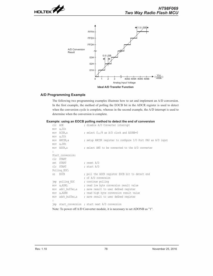
Rev. 1.10 78 ovee 01 Rev. 1.10 79 ovee 01
HT98F069Two Way Radio Flash MCU
HT98F069Two Way Radio Flash MCU
Ideal A/D Transfer Function
A/D Programming ExampleThefollowingtwoprogrammingexamplesillustratehowtosetandimplementanA/Dconversion.Inthefirstexample, themethodofpollingtheEOCBbit in theADCRregister isusedtodetectwhentheconversioncycleiscomplete,whereasinthesecondexample,theA/Dinterruptisusedtodeterminewhentheconversioniscomplete.
Example: using an EOCB polling method to detect the end of conversionclr ADE ; disable A/D Converter interruptmov a,01hmov ACSR,a ; select fSYS/8 as A/D clock and ADONB=0mov a,01hmov ANCSR,a ; setup ANCSR register to configure I/O Port PA0 as A/D inputmov a,00hmov ADCR,a ; select AN0 to be connected to the A/D converter:Start_conversion:clr STARTset START ; reset A/Dclr START ; start A/DPolling_EOC:sz EOCB ; poll the ADCR register EOCB bit to detect end ; of A/D conversionjmp polling_EOC ; continue pollingmov a,ADRL ; read low byte conversion result valuemov adrl_buffer,a ; save result to user defined registermov a,ADRH ; read high byte conversion result valuemov adrh_buffer,a ; save result to user defined register:jmp start_conversion ; start next A/D conversion
Note:TopoweroffA/DConvertermodule,itisnecessarytosetADONBas"1".

Rev. 1.10 78 ovee 01 Rev. 1.10 79 ovee 01
HT98F069Two Way Radio Flash MCU
HT98F069Two Way Radio Flash MCU
Example: using the interrupt method to detect the end of conversionclr ADE ; disable A/D Converter interruptmov a,01hmov ACSR,a ; select fSYS/8 as A/D clock and ADONB=0mov a,01hmov ANCSR,a ; setup ANCSR register to configure I/O Port PA0 as A/D inputmov a,00hmov ADCR,a ; select AN0 to be connected to the A/D converter::Start_conversion:clr STARTset START ; reset A/Dclr START ; start A/Dclr ADF ; clear A/D Converter interrupt request flagset ADE ; enable A/D Converter interruptset EMI ; enable global interrupt:: ; A/D Converter interrupt service routineADC_ISR:mov acc_stack,a ; save ACC to user defined memorymov a,STATUSmov status_stack,a ; save STATUS to user defined memory::mov a,ADRL ; read low byte conversion result valuemov adrl_buffer,a ; save result to user defined registermov a,ADRH ; read high byte conversion result valuemov adrh_buffer,a ; save result to user defined register::EXIT_ISR:mov a,status_stackmov STATUS,a ; restore STATUS from user defined memorymov a, acc_stack ; restore ACC from user defined memoryclr ADF ; clear A/D Converter interrupt flagreti
Note:TopoweroffA/DConvertermodule,itisnecessarytosetADONBas"1".

Rev. 1.10 80 ovee 01 Rev. 1.10 81 ovee 01
HT98F069Two Way Radio Flash MCU
HT98F069Two Way Radio Flash MCU
InterruptsInterruptsareanimportantpartofanymicrocontrollersystem.WhenanexternaleventoraninternalfunctionsuchasaTimer/EventCounter requiresmicrocontrollerattention, theircorrespondinginterruptwillenforceatemporarysuspensionofthemainprogramallowingthemicrocontrollertodirectattentiontotheirrespectiveneeds.
Thedevicecontainsonlyoneexternal interruptandmultiple internal interrupts.Theexternalinterrupt iscontrolledby theactionof theexternal interruptpin,while the internal interrupt iscontrolledbytheTimer/EventCounter,theA/Dconverterinterrupt,TimerBaseinterruptandAudioProcessor.
Interrupt RegisterOverallinterruptcontrol,whichmeansinterruptenablingandrequestflagsetting,iscontrolledbyusingregisters,INTC0andINTC1.Bycontrollingtheappropriateenablebitsintheregistereachindividual interruptcanbeenabledordisabled.Alsowhenaninterruptoccurs, thecorrespondingrequestflagwillbesetbythemicrocontroller.Theglobalenableflagclearedtozerowilldisableallinterrupts.
Eachregistercontainsanumberofenablebitstoenableordisableindividualregistersaswellasinterrupt flags to indicate thepresenceofan interrupt request.Thenamingconventionof thesefollowsaspecificpattern.Firstislistedanabbreviatedinterrupttype,thenthe(optional)numberofthatinterruptfollowedbyeitheran"E"forenable/disablebitor"F"forrequestflag.
Function Enable Bit Request Flag NoteGloal EMI — —IT Pin EIF EEI —Tie/Event Counte TnE TnF n=0~A/D Convete ADE ADF —Tie Base TBE TBF —Audio Pocesso AUPE AUPF —
Interrupt Register Bit Naming Conventions
Register Name
Bit7 6 5 4 3 2 1 0
ITC0 — T0F AUPF EIF T0E AUPE EEI EMIITC1 TBF ADF TF T1F TBE ADE TE T1E
Interrupt Registers List
INTC0 RegisterBit 7 6 5 4 3 2 1 0
ae — T0F AUPF EIF T0E AUPE EEI EMIR/W — R/W R/W R/W R/W R/W R/W R/WPOR — 0 0 0 0 0 0 0
Bit7 Unimplemented,readas"0"Bit6 T0F:Timer/EventCounter0interruptrequestflag
0:Norequest1:Interruptrequest
Bit5 AUPF:AudioProcessorinterruptrequestflag0:Norequest1:Interruptrequest

Rev. 1.10 80 ovee 01 Rev. 1.10 81 ovee 01
HT98F069Two Way Radio Flash MCU
HT98F069Two Way Radio Flash MCU
Bit4 EIF:INTpininterruptrequestflag0:Norequest1:Interruptrequest
Bit3 T0E:Timer/EventCounter0interruptcontrol0:Disable1:Enable
Bit2 AUPE:AudioProcessorinterruptcontrol0:Disable1:Enable
Bit1 EEI:INTpininterruptcontrol0:Disable1:Enable
Bit0 EMI:Globalinterruptcontrol0:Disable1:Enable
INTC1 Register Bit 7 6 5 4 3 2 1 0
ae TBF ADF TF T1F TBE ADE TE T1ER/W R/W R/W R/W R/W R/W R/W R/W R/WPOR 0 0 0 0 0 0 0 0
Bit7 TBF:TimeBaseinterruptrequestflag0:Norequest1:Interruptrequest
Bit6 ADF:A/Dconverterinterrruptrequestflag0:Norequest1:Interruptrequest
Bit5 T2F:Timer/EventCounter2interruptrequestflag0:Norequest1:Interruptrequest
Bit4 T1F:Timer/EventCounter1interruptrequestflag0:Norequest1:Interruptrequest
Bit3 TBE:TimeBaseinterruptcontrol0:Disable1:Enable
Bit2 ADE:A/Dconverterinterruptcontrol0:Disable1:Enable
Bit1 T2E:Timer/EventCounter2interruptcontrol0:Disable1:Enable
Bit0 T1E:Timer/EventCounter1interruptcontrol0:Disable1:Enable

Rev. 1.10 8 ovee 01 Rev. 1.10 83 ovee 01
HT98F069Two Way Radio Flash MCU
HT98F069Two Way Radio Flash MCU
Interrupt OperationATimer/EventCounteroverflow,acompletionofA/Dconversionoranactiveedgeontheexternalinterruptpin,etc.,willallgenerateaninterruptrequestbysettingtheircorrespondingrequestflag,iftheirappropriateinterruptenablebitisset.Whenthishappens,theProgramCounter,whichstorestheaddressofthenextinstructiontobeexecuted,willbetransferredontothestack.TheProgramCounterwill thenbe loadedwithanewaddresswhichwillbe thevalueof thecorrespondinginterruptvector.Themicrocontrollerwillthenfetchitsnextinstructionfromthisinterruptvector.
Theinstructionat thisvectorwillusuallybeaJMPstatementwhichwill jumptoanothersectionofprogramwhichisknownastheinterruptserviceroutine.Hereislocatedthecodetocontroltheappropriate interrupt.The interruptserviceroutinemustbe terminatedwithaRETI instruction,whichretrievestheoriginalProgramCounteraddressfromthestackandallowsthemicrocontrollertocontinuewithnormalexecutionatthepointwheretheinterruptoccurred.
Thevarious interruptenablebits, togetherwith theirassociatedrequest flags,areshownin thefollowingdiagramwiththeirorderofpriority.
04H
0CH
18H
Vector
Low
PioityHigh
RequestFlags
EnaleBits
MasteEnale
EMI auto disaled in ISR
Inteuptae
EMI
EMI
EMIEIFIT Pin EEI
T0FTie/Event Counte 0 T0E
ADFA/D Convete ADE
Legend
xxF Request Flag - auto eset in ISR
xxE Enale Bit
1CHEMITBFTie Base TBE
08HEMIAUPFAudio Pocesso AUPE
10HEMIT1FTie/Event Counte 1 T1E
14HEMITFTie/Event Counte TE
Interrupt Structure
Onceaninterruptsubroutineisserviced,alltheotherinterruptswillbeblocked,astheEMIbitwillbeclearedautomatically.Thiswillpreventanyfurtherinterruptnestingfromoccurring.However,ifotherinterruptrequestsoccurduringthisinterval,althoughtheinterruptwillnotbeimmediatelyserviced,therequestflagwillstillberecorded.Ifaninterruptrequiresimmediateservicingwhiletheprogramisalreadyinanotherinterruptserviceroutine,theEMIbitshouldbesetafterenteringtheroutine,toallowinterruptnesting.Ifthestackisfull,theinterruptrequestwillnotbeacknowledged,eveniftherelatedinterruptisenabled,untiltheStackPointerisdecremented.Ifimmediateserviceisdesired,thestackmustbepreventedfrombecomingfull.
Whenaninterruptrequestisgeneratedittakes2or3instructioncyclesbeforetheprogramjumpstotheinterruptvector.IfthedeviceisintheSleepModeandiswokenupbyaninterruptrequestthenitwilltake3cyclesbeforetheprogramjumpstotheinterruptvector.

Rev. 1.10 8 ovee 01 Rev. 1.10 83 ovee 01
HT98F069Two Way Radio Flash MCU
HT98F069Two Way Radio Flash MCU
MainPoga
Enale it set?
MainPoga
Autoatically Disale Inteupt Clea EMI & Request Flag
Wait fo ~3 Instuction Cycles
ISR Enty......
RETI(it will set EMI autoatically)
Inteupt Request oInteupt Flag Set y Instuction
Y
Interrupt Flow
Interrupt PriorityInterrupts,occurringintheintervalbetweentherisingedgesoftwoconsecutiveT2pulses,willbeservicedonthelatterofthetwoT2pulses,if thecorrespondinginterruptsareenabled.Incaseofsimultaneousrequests,thefollowingtableshowstheprioritythatisapplied.ThesecanbemaskedbyresettingtheEMIbit.
Interrupt Source Priority VectorExtenal inteupt 1 04HAudio Pocesso inteupt 08HTie/Event Counte 0 overflow 3 0CHTie/Event Counte 1 overflow 4 10HTie/Event Counte overflow 14HA/D convete coplete 18HTime Base Overflow 7 1CH
Incaseswherebothexternalandinternalinterruptsareenabledandwhereanexternalandinternalinterruptoccurssimultaneously,theexternalinterruptwillalwayshavepriorityandwillthereforebeservicedfirst.Suitablemaskingoftheindividualinterruptsusingtheinterruptregisterscanpreventsimultaneousoccurrences.

Rev. 1.10 84 ovee 01 Rev. 1.10 8 ovee 01
HT98F069Two Way Radio Flash MCU
HT98F069Two Way Radio Flash MCU
External InterruptTheINTpinfunction,whichispin-sharedwithPA3bydefaultoption,canberemappedtoPB4bysettingthePCFGbitintheCTRL0registerto"1".
Foranexternalinterrupttooccur,theglobalinterruptenablebit,EMI,andexternalinterruptenablebit,EEI,mustfirstbeset.Anactualexternalinterruptwill takeplacewhentheexternalinterruptrequestflag,EIFisset,asituationthatwilloccurwhenanedgetransitionappearsontheexternalINTpin.Thetypeoftransitionthatwill triggeranexternalinterrupt,whetherhightolow,lowtohighorbothisdeterminedbytheINTEG0andINTEG1bits,whicharebits6and7respectivelyintheCTRL1controlregister.Thesetwobitscanalsodisabletheexternalinterruptfunction.
INTEG1 INTEG0 Edge Trigger Type0 0 Extenal inteupt disale0 1 Rising edge tigge1 0 Falling edge tigge1 1 Dual edge tigge
Theexternalinterruptpinispin-sharedwiththeI/Opinandcanonlybeusedasanexternalinterruptpin if thecorrespondingexternal interruptenablebit in theINTC0registerhasbeensetandtheedgetriggertypehasbeenselectedusingtheCTRL1register.Thepinmustalsobesetasaninputbysettingthecorrespondingbitintheportcontrolregister.Whentheinterruptisenabled,thestackisnotfullanda transitionappearsontheexternal interruptpin,asubroutinecall to theexternalinterruptvector,willtakeplace.Whentheinterruptisserviced,theexternalinterruptrequestflag,EIF,willbeautomatically resetand theEMIbitwillbeautomaticallycleared todisableotherinterrupts.Notethatanypull-highresistorconnectionsonthispinwillremainvalidevenifthepinisusedasanexternalinterruptinput.
Timer/Event Counter InterruptFor aTimer/EventCounter interrupt tooccur, theglobal interrupt enablebit,EMIand thecorresponding timer interruptenablebitTnEmust firstbeset.AnactualTimer/EventCounterinterruptwilltakeplacewhentheTimer/EventCounterrequestflagTnFisset,asituationthatwilloccurwhentherelevantTimer/EventCounteroverflows.Whentheinterruptisenabled,thestackisnotfullandaTimer/EventCounteroverflowoccurs,asubroutinecalltotherelevanttimerinterruptvector,willtakeplace.Whentheinterruptisserviced,thetimerinterruptrequestflagTnFwillbeautomaticallyresetandtheEMIbitwillbeautomaticallyclearedtodisableotherinterrupts.
A/D Converter InterruptForanA/Dinterrupttooccur,theglobalinterruptenablebitEMIandthecorrespondinginterruptenablebitADEmustbefirstset.AnactualA/Dinterruptwill takeplacewhentheA/DconverterrequestflagADFisset,asituationthatwilloccurwhenanA/Dconversionprocesshascompleted.Whentheinterruptisenabled,thestackisnotfullandanA/Dconversionprocessfinishesexecution,asubroutinecalltotherelevantA/Dinterruptvector,willtakeplace.Whentheinterruptisserviced,theA/DinterruptrequestflagADFwillbeautomaticallyresetandtheEMIbitwillbeautomaticallyclearedtodisableotherinterrupts.

Rev. 1.10 84 ovee 01 Rev. 1.10 8 ovee 01
HT98F069Two Way Radio Flash MCU
HT98F069Two Way Radio Flash MCU
Time Base InterruptForaTimeBaseinterrupttooccur,theglobalinterruptenablebitEMIandthecorrespondinginterruptenablebitTBE,mustfirstbeset.AnactualTimeBaseinterruptwilltakeplacewhentheTimeBaserequestflagTBFisset,asituationthatwilloccurwhentheTimeBaseoverflows.Whentheinterruptisenabled, thestack isnot fullandaTimeBaseoverflowoccursasubroutinecall toTimeBaseinterruptvectorwilltakeplace.Whentheinterruptisserviced,theTimeBaseinterruptflagTBFwillbeautomaticallyresetandtheEMIbitwillbeautomaticallyclearedtodisableotherinterrupts.
Audio Processor InterruptTheAudioProcessorinterruptisinitialisedbysettingtheAudioProcessorrequestflag,AUPF.WhentheAudioProcessorreturnsadata, theSPIRQbit intheSPICRregister transitsfrom"1"to"0",whichwilltriggeraninterruptrequest.Iftheinterruptisenabled,thestackisnotfullandtheAUPFisset,asubroutinecall to theAudioProcessor interruptvectorwilloccur.Whentheinterrupt isserviced,therelatedinterruptrequestflagAUPFwillberesetandtheEMIbitwillbeautomaticallyclearedtodisablefurtherinterrupts.
Interrupt Wake-up FunctionEachof the interruptfunctionshas thecapabilityofwakingupthemicrocontrollerwhenin theSleeporIdleMode.Awake-upisgeneratedwhenaninterruptrequestflagchangesfromlowtohighandis independentofwhether theinterrupt isenabledornot.Therefore,eventhoughthedeviceis intheSleeporIdleModeanditssystemoscillatorisstopped,situationssuchasexternaledgetransitionsontheexternalinterruptpinsmaycausetheirrespectiveinterruptflagtobesethighandconsequentlygenerateaninterrupt.Caremustthereforebetakenifspuriouswake-upsituationsaretobeavoided.Ifaninterruptwake-upfunctionis tobedisabledthenthecorrespondinginterruptrequestflagshouldbesethighbeforethedeviceenterstheSleepMode.Theinterruptenablebitshavenoeffectontheinterruptwake-upfunction.
Programming ConsiderationsBydisablingtherelevantinterruptenablebits,arequestedinterruptcanbepreventedfrombeingserviced,however,oncean interrupt request flag is set, itwill remain in thiscondition in theinterruptregisteruntilthecorrespondinginterruptisservicedoruntiltherequestflagisclearedbytheapplicationprogram.
It isrecommendedthatprogramsdonotusethe"CALL"instructionwithintheinterruptservicesubroutine.Interruptsoftenoccurinanunpredictablemannerorneedtobeservicedimmediately.Ifonlyonestackisleftandtheinterruptisnotwellcontrolled,theoriginalcontrolsequencewillbedamagedonceaCALLsubroutineisexecutedintheinterruptsubroutine.
Every interrupthas thecapabilityofwakingup themicrocontrollerwhen it is inSleepor IdleMode,thewakeupbeinggeneratedwhentheinterruptrequestflagchangesfromlowtohigh.IfitisrequiredtopreventacertaininterruptfromwakingupthemicrocontrollerthenitsrespectiverequestflagshouldbefirstsethighbeforeenteringtheSleeporIdleMode.
AsonlytheProgramCounterispushedontothestack,thenifthecontentsoftheaccumulator,statusregisterorotherregistersarealteredbytheinterruptserviceprogram,whichmaycorruptthedesiredcontrolsequence,thenthecontentsshouldbesavedinadvance.
Toreturnfromaninterruptsubroutine,eitheraRETorRETIinstructionmaybeexecuted.TheRETIinstructioninadditiontoexecutingareturntothemainprogramalsoautomaticallysetstheEMIbithightoallowfurther interrupts.TheRETinstructionhoweveronlyexecutesareturntothemainprogramleavingtheEMIbitinitspresentzerostateandthereforedisablingtheexecutionoffurtherinterrupts.

Rev. 1.10 8 ovee 01 Rev. 1.10 87 ovee 01
HT98F069Two Way Radio Flash MCU
HT98F069Two Way Radio Flash MCU
Low Voltage Detector – LVDThedevicehasaLowVoltageDetectorfunction,alsoknownasLVD.Thisenabledthedevicetomonitorthepowersupplyvoltage,VDD,andprovideawarningsignalshoulditfallbelowacertainlevel.Thisfunctionmaybeespeciallyusefulinbatteryapplicationswherethesupplyvoltagewillgraduallyreduceasthebatteryages,asitallowsanearlywarningbatterylowsignaltobegenerated.
LVD RegisterTheLowVoltageDetectorfunctioniscontrolledusingasingleregisterwiththenameLVDC.Threebitsinthisregister,VLVD2~VLVD0,areusedtoselectoneofeightfixedvoltagesbelowwhichalowvoltageconditionwillbedetermined.AlowvoltageconditionisindicatedwhentheLVDObit isset.IftheLVDObitislow,thisindicatesthattheVDDvoltageisabovethepresetlowvoltagevalue.TheLVDENbitisusedtocontroltheoverallon/offfunctionofthelowvoltagedetector.Settingthebithighwillenablethelowvoltagedetector.Clearingthebittozerowillswitchofftheinternallowvoltagedetectorcircuits.Asthelowvoltagedetectorwillconsumeacertainamountofpower,itmaybedesirabletoswitchoffthecircuitwhennotinuse,animportantconsiderationinpowersensitivebatterypoweredapplications.
LVDC RegisterBit 7 6 5 4 3 2 1 0
ae — — LVDO LVDE — VLVD VLVD1 VLVD0R/W — — R R/W — R/W R/W R/WPOR — — 0 0 — 0 0 0
Bit7~6 Unimplemented,readas"0"Bit5 LVDO:LVDOutputflag
0:NoLowVoltageDetected1:LowVoltageDetected
Bit4 LVDEN:LowVoltageDetectorEnablecontrol0:Disable1:Enable
Bit3 Unimplemented,readas"0"Bit2~0 VLVD2~VLVD0:LVDVoltageselection
000:2.0V001:2.2V010:2.4V011:2.7V100:3.0V101:3.3V110:3.6V111:4.0V

Rev. 1.10 8 ovee 01 Rev. 1.10 87 ovee 01
HT98F069Two Way Radio Flash MCU
HT98F069Two Way Radio Flash MCU
LVD OperationTheLowVoltageDetectorfunctionoperatesbycomparingthepowersupplyvoltage,VDD,withapre-specifiedvoltagelevelstoredintheLVDCregister.Thishasarangeofbetween2.0Vand4.0V.Whenthepowersupplyvoltage,VDD,fallsbelowthispre-determinedvalue,theLVDObitwillbesethighindicatinga lowpowersupplyvoltagecondition.TheLowVoltageDetectorfunctionissuppliedbyareferencevoltagewhichwillbeautomaticallyenabled.Whenthedeviceispowereddown,thelowvoltagedetectorwillremainactiveiftheLVDENbitishigh.AfterenablingtheLowVoltageDetector,atimedelaytLVDSshouldbeallowedforthecircuitrytostabilisebeforereadingtheLVDObit.NotealsothatastheVDDvoltagemayriseandfallratherslowly,atthevoltagenearsthatofVLVD,theremaybemultiplebitLVDOtransitions.
VDD
LVDE
LVDO
VLVD
tLVDS
LVD Operation

Rev. 1.10 88 ovee 01 Rev. 1.10 89 ovee 01
HT98F069Two Way Radio Flash MCU
HT98F069Two Way Radio Flash MCU
SPI FunctionTheSPIinterfaceisonemethodtocommunicatewithAudioProcessor.ThecommandgrouptypescanbereferredinchapterofMCUInterfacing.
SPIformatandcontrolregisterareshownbelow.
SPICR Register Bit 7 6 5 4 3 2 1 0
ae IEMC — ERAM SPISS SPICK MOSI MISO SPIRQR/W R/W — R/W R/W R/W R/W R RPOR 1 — 0 1 0 0 x x
"x": unknownBit7 IEMC:Modecontrolbit
0:ExternalMCUmode(padcontrol)–PA5/PC4/PC5/PC6/PC7pinsareusedasMISO/MOSI/SPIRQ/SPICK/SPISSpinfunctionsrespectively
1:Internalmode(MCUcontrol)In theexternalMCUmode, theAudioProcessorcanbecontrolledbyanexternalMCUviatheSPIinterface.SPISS/SPICK/MOSIcannotbereadorwrittenandMISO/SPIRQisreadonlywhenanSPIRQfallingedgeoccurs,itwillnotaffectAUPFflagtogenerateaninterrupt.
Bit6 Unimplemented,readas"0"Bit5 ERAM:PB4/PB5/PB6/PB7pinsareusedasAudioProcessorGPIO0/1/2/3respectively
0:Disable1:Enable
Bit4 SPISS:SelectAudioProcessor0:Select1:Notselect
Bit3 SPICK:SPIclockoutputtoAudioProcessor0:Low1:High
Bit2 MOSI:Outputcommand/dataintoAudioProcessor0:Low1:High
Bit1 MISO:Inputcommand/datafromAudioProcessorBit0 SPIRQ:Thisbitisclearedto0byAudioprocessorwhentheAudioprocessorinterrupt
occurs.Thisbitwillbesetto1byAudioprocessoraftertheMCUhasreadcommand/datasuccessfully.
SPISS
MOSI
MISO
C2 C1 C0 D15 D14 D13 D12 D11 D10 D9 D8 D7 D6 D5 D4 D3 D2 D1 D0
C2 C1 C0 D15 D14 D13 D12 D11 D10 D9 D8 D7 D6 D5 D4 D3 D2 D1 D0
C3
C3
SPIRQ
SPICK
C2 C1 C0 D15 D14 D13 D12 D11 D10 D9 D8 D7 D6 D5 D4 D3 D2 D1 D0
C2 C1 C0 D15 D14 D13 D12 D11 D10 D9 D8 D7 D6 D5 D4 D3 D2 D1 D0
C3
C3

Rev. 1.10 88 ovee 01 Rev. 1.10 89 ovee 01
HT98F069Two Way Radio Flash MCU
HT98F069Two Way Radio Flash MCU
BEEP FunctionThis functionusesapplicationprogramtobuildasquarewaveonspeakerorAudioProcessorthroughBEEP0/1pad.
BDR RegisterBit 7 6 5 4 3 2 1 0
ae — — — — — — BEEP1 BEEP0R/W — — — — — — R/W R/WPOR — — — — — — 0 0
Bit7~2 Unimplemented,readas"0"Bit1 BEEP1:outputsignal
0:Low1:High
WhentheBEEP1functionisusefulandisselectedasAudioProcessorsource, theBEEP1padisconnectedtoAudioProcessor.
Bit0 BEEP0:outputsignal0:Low1:High
WhentheBEEP0functionisusefulandisselectedasAudioProcessorsource, theBEEP0padisconnectedtospeaker.Thesetwobitsareoutputpinsignals,settingorclearingBDRregisterdatacanmodifytheBEEP0/BEEP1status.Ifthetwofunctionsarenotuseful,modifyingtheBEEP0/BEEP1datawillnotaffecttheBEEP0/BEEP1padstatus.
Digital to Analog Converter – DACThedeviceincludesa4-channel8-bitDigital toAnalogConverterfunction.Thisfunctionallowsdigitaldatacontainedinthedevicetogenerateaudiosignals.
OperationThedata tobeconvertedisstoredinfourregisters,DA0R,DA1R,DA2RandDA3R.ThefourbitsinthecontrolregisterDACRprovidesDACnon/offcontrol.TheDACnoutputsarechanneledtopinsDAO0~DAO3whicharepin-sharedwithI/OpinsPB0~PB3.WhentheDACnisenabledbysettingtheENnhigh,thentheoriginalI/Ofunctionwillbedisabled,alongwithanypull-highresistoroptions.TheDACoutputreferencevoltageisthepowersupplyvoltageVDD.
DACR RegisterBit 7 6 5 4 3 2 1 0
ae — — — — E3 E E1 E0R/W — — — — R/W R/W R/W R/WPOR — — — — 0 0 0 0
Bit7~4 Unimplemented,readas"0"Bit3 EN3:DAC3disable/enablecontrol
0:Disable1:Enable
Bit2 EN2:DAC2disable/enablecontrol0:Disable1:Enable

Rev. 1.10 90 ovee 01 Rev. 1.10 91 ovee 01
HT98F069Two Way Radio Flash MCU
HT98F069Two Way Radio Flash MCU
Bit1 EN1:DAC1disable/enablecontrol0:Disable1:Enable
Bit0 EN0:DAC0disable/enablecontrol0:Disable1:Enable
DA3R RegisterBit 7 6 5 4 3 2 1 0
ae DA37 DA3 DA3 DA34 DA33 DA3 DA31 DA30R/W R/W R/W R/W R/W R/W R/W R/W R/WPOR x x x x x x x x
"x" unknownBit7~0 DA37~DA30:DAC3outputdata
DA2R RegisterBit 7 6 5 4 3 2 1 0
ae DA7 DA DA DA4 DA3 DA DA1 DA0R/W R/W R/W R/W R/W R/W R/W R/W R/WPOR x x x x x x x x
"x" unknownBit7~0 DA27~DA20:DAC2outputdata
DA1R RegisterBit 7 6 5 4 3 2 1 0
ae DA17 DA1 DA1 DA14 DA13 DA1 DA11 DA10R/W R/W R/W R/W R/W R/W R/W R/W R/WPOR x x x x x x x x
"x" unknownBit7~0 DA17~DA10:DAC1outputdata
DA0R RegisterBit 7 6 5 4 3 2 1 0
ae DA07 DA0 DA0 DA04 DA03 DA0 DA01 DA00R/W R/W R/W R/W R/W R/W R/W R/W R/WPOR x x x x x x x x
"x" unknownBit7~0 DA07~DA00:DAC0outputdata

Rev. 1.10 90 ovee 01 Rev. 1.10 91 ovee 01
HT98F069Two Way Radio Flash MCU
HT98F069Two Way Radio Flash MCU
Audio ProcessorThedeviceincludesanaudioprocessorfunctionforprocessingofsignalsreceivedontheRFcarrier.Aimingspecificallyatlowcostradiocommunicationproducts,theaudioprocessorsectioncontainsall thetransmitterandreceiverfunctionsrequiredtoprocessthenecessaryin-bandaudiosignalssuchascompression,expansion,scramblingandde-scrambling.
Audio ReceiverThefollowingdiagramshowsthemainfunctionalblocksofthereceiveraudioprocessor.
PGA
BUF
ADCDEMOD
AUXVAG
BEEP1
LPF270
HPF300
CTCSS Decoder
NARROW/WIDE BAND
DCS Decoder
DTMF Decoder
DEEMPHASIS EXPANDER DESCRAMBLE
I/O:1EHI/O:1BH
I/O:1EHI/O:1BH
I/O:2CH
I/O:2CH I/O:2CH I/O:2CH,CLI:12B I/O:2CH,CLI:13A,13B
I/O:11H,22H,23H,2EH,CLI: 324,325
I/O:11H,22H,23H,2FHCLI:1C4
I/O:11H,22H,23H,2BH,30H,31HCLI:1DD,1DE,4CA,4D0,4D1,4D6,4DB,4DE
I/O:11H,22H,2BHCLI:1DD,1DE,1E2,4DC,4DD,4DE
AUDOBEEP0PGAI_S[7:5] PGAI_B[4:0]
EN_PGA
EN_BUFAUDO_S[4:2]
User Tone Decoder
I/O:11H,22H,23HCLI:4D9,4DAMIC_O
EN_DAC1
I/O:1EH
Selecte Call Decoder
Note:“I/O:XXH”standsforI/Ocommand,“CLI:xxx”standsforCLIcommand.Receiver Block Diagram

Rev. 1.10 9 ovee 01 Rev. 1.10 93 ovee 01
HT98F069Two Way Radio Flash MCU
HT98F069Two Way Radio Flash MCU
Receiver Audio FiltersTheincomingsignalisfirstfiltered,asshownintheblockdiagram,toremovesub-audiocomponentsandtofilterouthighfrequencynoise.Afterthislowandhighpassfilteringisexecuted,theresidualaudiosignalisthenroutedtotheAudiooutputpin,AUDO.Individualfiltersareavailableforthefollowing:• 300HzHighPassforrejectionofsubaudiosignals• 2.55kHzLowPassforNarrowBandwidthchanneloperation• 3.0kHzLowPassforWideBandwidthchanneloperation
Receiver Audio Filter Frequency Response
Receiver De-emphasisThedeviceincludesaselectablede-emphasisfilterwitharesponseasshowninthefollowingfigure.
Audio Frequency De-emphasis

Rev. 1.10 9 ovee 01 Rev. 1.10 93 ovee 01
HT98F069Two Way Radio Flash MCU
HT98F069Two Way Radio Flash MCU
Receiver De-scramblerIfdesired,thetransmittersectionofthedevicecanbesetuptoscramblethetransmittedaudiosignalsby inversing the transmittedaudiofrequencies. In the receivermode,adescrambler isused toconvertthereceivedscrambledsignalsbacktotheiroriginalaudiofrequencycontent.TheinversioncentralfrequencycanbeprogrammedusingtheCLIScramblerInversionFrequencyregisters.Thedefaultinversioncentralfrequencyvalueis3300Hz.
Receiver ExpanderThereceiversection includesanexpander function toexpandanysignals thatmayhavebeencompressedby the transmitter.This function isoptionaland isonlyused if the transmitter istransmittingcompressedsignals.Compressingandexpandingtheaudiosignalsincreasethesignaldynamicrangegreatly.
Receiving and Decoding CTCSS or DCS CodesThedevicecanaccuratelydetectvalidCTCSStonesrapidlywhichpreventslosingthestartofaudioordatatransmissions.Itcanalsocontinuouslymonitorthedetectedtonestoensurelowriskoffalsedropout.TheDCScodeisinNRZformatandistransmittedatarateof134.4±0.4bps.Thedeviceisabletodecodeany23-bitpatternineitherofthetwoDCSmodulationmodesasdefinedbyTIA/EIA-603.ThedevicecanalsodetectvalidDCScodequicklyenoughtoavoidlosingthebeginningofaudiotransmissions.
Rx In-Band Tone DecoderThe in-band tonecanbesummarised intoSelectivecall,DTMFandUser-tonecategories.ForSelectivecall,thedevicewilldecodeasetofEEAdefinedtonesets,howeverthismaybechangedbytheuserstoanyvalidtonesetswithinitsoperationalrangebysettingtherelatedregisters.Thisensuresthat thedevicecanremaincompatiblewithallavailabletonesystemsinuse.Thedevicedoesnot implementautomatic repeat tone insertionordeletionas thisdependsupon theuserprotocol.
Audio TransmitterThefollowingdiagramshowsthemainfunctionblocksofthetransmitteraudioprocessor.
AMP1
AMP2
DAC1
DAC2
User Tone Generrator
DTMF Generrator
Selective CallGenerator
DCS & DCS OFF TONE
Generator
CTCSS & CTCSS OFF TONEGenerator
MIC_IOPA
MIC_O
VAG
NARROW/WIDE BAND EMPHASISCOMPRESSORSCRAMBLEHPF300 M
UX
VR1
VR5
VR4
VR3
VR2
I/O:1BH I/O:1EH
I/O:1EH
I/O:1EH
I/O:1EH
I/O:1BH
I/O:1BH
I/O:2CH I/O:2CHI/O:11H,2CHCLI:13A,13B I/O:2CH,CLI:12A I/O:2CH
I/O:11H,CLI:4D9,4DA
I/O:11H,2DH
I/O:11H,2AH
I/O:11H,2BH
I/O:11H,2BH,31H
MODO
SMOD
EN_MIC EN_AMP1
EN_AMP2
SDAO1
SDAO2
EN_DAC1
EN_DAC2
PGAAUXVAG
BEEP1
I/O:1EHI/O:1BH
PGAI_S[7:5] PGAI_B[4:0]EN_PGA
ADCDEMOD
Note:“I/O:XXH”standsforI/Ocommand,“CLI:xxx”standsforCLIcommand.Transmitter Block Diagram

Rev. 1.10 94 ovee 01 Rev. 1.10 9 ovee 01
HT98F069Two Way Radio Flash MCU
HT98F069Two Way Radio Flash MCU
Transmitter Audio Filters Thetransmitteraudiofiltersincludea25kHzwide-bandanda12.5kHznarrow-bandchannelfilter.Thefilterfrequencyresponsesareshowninthefollowingfigure.
Transmitter Audio Filter Frequency Response
Transmitter Pre-emphasisThedeviceincludesaselectablepre-emphasisfilterwith+6dBperoctavefrom300Hzto3000Hz,witharesponseasshowninthefollowingfigure.
Transmitter Audio Frequency Pre-emphasis

Rev. 1.10 94 ovee 01 Rev. 1.10 9 ovee 01
HT98F069Two Way Radio Flash MCU
HT98F069Two Way Radio Flash MCU
Transmitter ScramblerThedeviceincludesanoptionalfrequencyinversionscramblerforbothtransmitandreceivemodes.Itscramblesthetransmittedaudiobandsignals,whichcanthenbede-scrambledinthereceiver.Thecentralinversionfrequencyisprogrammedusingregisters.Thedefaultvalueis3300Hz.ThecentralinversionfrequencycanbechangednotonlyintheIdlemodebutalsointheactiveRxorTxmode.
Transmitter CompressorThedevice incorporatesanoptionalsyllabiccompandorforboth transmitandreceivemode. Itcompressestheaudiobandsignalsbeforetransmissiontoenhancetheoveralldynamicrange.Therelationshipbetweentheinputandoutputvoltageofthecompandorisshowninthefollowingfigure.
Compander Voltage-Voltage Response
Transmitter Sub-audio EncodersSub-audiosignaling isavailable in theaudiobandbelow260Hz.Whensub-audiosignaling isenabled, the300HzHPF in theaudiosectionshouldalsobeenabled to remove thesub-audiosignalingfromtheactualaudiosignals(forbothTxandRx).BothCTCSStonesandDCScodesaresupported.Inadditiontothe51definedCTCSStones,userscandefinetheirspecifiedtonesusingregisters.TheDCScoder/decoderincludesa23-bitmodewithbothnormalandinversemodulationformatsanda134Hzendoftransmissionburst.
Transmitter In-Band SignalingThedevice includesaprogrammable in-band tonesetoranarbitrarysingleuser-tonebetween300Hzand3000Hz.Bydefault,thedevicewilluseanEEAselectivecalldefinedtoneset,howeverthismaybechangedtoanyvalidtonewithinitsoperationalrangeusingregisters.Inadditiontotheselectivecalldefinedtonesets,standarddualtonemultiplefrequency,DTMF,isalsosupportedinthein-bandsignalingmode.

Rev. 1.10 9 ovee 01 Rev. 1.10 97 ovee 01
HT98F069Two Way Radio Flash MCU
HT98F069Two Way Radio Flash MCU
Supported Different Combination Functions
ReceiverVoice Band Processing Sub Tone Audio Tone
(DTMF/Selective Call/User-tone)
Basic Voice Filte
inv DCS, DCS/ User-defined DCS Decoder DTMF DecodeCTCSS/ User-defined CTCSS Decoder DTMF Decodeinv DCS, DCS/ User-defined DCS Decoder Selective Call / Use-tone DecodeCTCSS/ User-defined CTCSS Decoder Selective Call / Use-tone Decode
Basic Voice Filte + De-ephasis
inv DCS, DCS/ User-defined DCS Decoder DTMF DecodeCTCSS/ User-defined CTCSS Decoder DTMF Decodeinv DCS, DCS/ User-defined DCS Decoder Selective Call Decode/ Use-toneCTCSS/ User-defined CTCSS Decoder Selective Call Decode/ Use-tone
Basic Voice Filte + Expande
inv DCS, DCS/ User-defined DCS Decoder DTMF DecodeCTCSS/ User-defined CTCSS Decoder DTMF Decodeinv DCS, DCS/ User-defined DCS Decoder Selective Call Decode/ Use-toneCTCSS/ User-defined CTCSS Decoder Selective Call Decode/ Use-tone
Basic Voice Filte + De-ephasis + Expande
inv DCS, DCS/ User-defined DCS Decoder DTMF DecodeCTCSS/ User-defined CTCSS Decoder DTMF Decodeinv DCS, DCS/ User-defined DCS Decoder Selective Call Decode/ Use-toneCTCSS/ User-defined CTCSS Decoder Selective Call Decode/ Use-tone
Basic Voice Filte + De-ephasis + Expande + De-Scale
inv DCS, DCS/ User-defined DCS Decoder DTMF Decode
CTCSS/ User-defined CTCSS Decoder DTMF Decode
Transmitter Voice Band Processing Sub Tone Audio Tone
(DTMF/Selective Call/User-tone)
Basic Voice Filte
inv DCS, DCS/ User-defined DCS Encoder DTMF EncodeCTCSS/ User-defined CTCSS Encoder DTMF Encodeinv DCS, DCS/ User-defined DCS Encoder Selective Call / Use-tone EncodeCTCSS/ User-defined CTCSS Encoder Selective Call / Use-tone Encode
Basic Voice Filte + Ephasis
inv DCS, DCS/ User-defined DCS Encoder DTMF EncodeCTCSS/ User-defined CTCSS Encoder DTMF Encodeinv DCS, DCS/ User-defined DCS Encoder Selective Call / Use-tone EncodeCTCSS/ User-defined CTCSS Encoder Selective Call / Use-tone Encode
Basic Voice Filte + Copess
inv DCS, DCS/ User-defined DCS Encoder DTMF EncodeCTCSS/ User-defined CTCSS Encoder DTMF Encodeinv DCS, DCS/ User-defined DCS Encoder Selective Call / Use-tone EncodeCTCSS/ User-defined CTCSS Encoder Selective Call / Use-tone Encode
Basic Voice Filte + Ephasis + Copess
inv DCS, DCS/ User-defined DCS Encoder DTMF EncodeCTCSS/ User-defined CTCSS Encoder DTMF Encodeinv DCS, DCS/ User-defined DCS Encoder Selective Call / Use-tone EncodeCTCSS/ User-defined CTCSS Encoder Selective Call / Use-tone Encode
Basic Voice Filte + Ephasis + Copess + Scale
inv DCS, DCS/ User-defined DCS Encoder DTMF Encode
CTCSS/ User-defined CTCSS Encoder DTMF Encode
Note:Thevoicebandandaudiotonemustbeprocessedseparatelyinthetransmitter.

Rev. 1.10 9 ovee 01 Rev. 1.10 97 ovee 01
HT98F069Two Way Radio Flash MCU
HT98F069Two Way Radio Flash MCU
Audio Signal RoutingThedevicehasaflexibleaudiosignalroutinginputandoutputstructuretoroutesignalstoandfromtheaudioprocessor.Theroutingsetuppathiscontrolledusingthepathselectionregisterwhichisdescribedinadifferentsection.ThegainoftheinternalProgrammableGainAmplifiershownintheblockdiagramisalsosetupusingaregister,thedetailsofwhicharedescribedinadifferentsection.
DEMOD1
VAG2
VAGREF3
VCCA14
AUX5
PE16
PE07
SMOD8
MODO9
AUDO10
VCCA211
VSSA212
PB0
13
PB1
14
PB2
15
PB3
16
PD2
17
PD3
18
PB4
19
PB5
20
PLLC
21
XIN
22
XOUT
23
VSS
24
VDD 25PB6 26PB7 27PA0 28PA1 29PA2 30PA3 31PC0 32PC1 33PC2 34PC3 35PA7 36
PA6
37PA
538
PA4
39PC
440
PC5
41PC
642
PC7
43PD
044
PD1
45VSS
A1
46MIC_0
47MIC_1
48U1
HT98F069_48LQFP
10KR1 62KR2
10KR3
10KR4
10KR5
1uFC1
1uFC2
1uFC3
1uFC5
1uFC7
1uFC9
4nFC6
4nFC8
4nFC10 0.1uF
C18102pF
C19
SQI
SQI
AVSS
AVSSDVSS
DVSS
AVSSAVSS
MIC & driver circuit
AVSS
VCC2
VCC
VCC1
Speaker out
RF Block
Audio Signal Routing Block Diagram

Rev. 1.10 98 ovee 01 Rev. 1.10 99 ovee 01
HT98F069Two Way Radio Flash MCU
HT98F069Two Way Radio Flash MCU
MCU InterfacingTheAudioProcessorcommunicateswiththeintegratedMCUusingaseriesofcommandregisters.CommunicationwithexternalMCUsisconductedusingtheSPICRregisterandthePC4~PC7I/OlineswhichhaveshareduseasanSPIinterface.
SPISS
SPICK
MOSI
MISO
C2 C1 C0 D15 D14 D13 D12 D11 D10 D9 D8 D7 D6 D5 D4 D3 D2 D1 D0
C2 C1 C0 D15 D14 D13 D12 D11 D10 D9 D8 D7 D6 D5 D4 D3 D2 D1 D0
C3
C3
SPIRQ
C2 C1 C0 D15 D14 D13 D12 D11 D10 D9 D8 D7 D6 D5 D4 D3 D2 D1 D0
C2 C1 C0 D15 D14 D13 D12 D11 D10 D9 D8 D7 D6 D5 D4 D3 D2 D1 D0
C3
C3
SPISSfromtheMCU:Thispinisaninputpinandisactivelow.
SPICKfromtheMCU:Thispinistheclocksourceinputpin.
MOSI(SMOSI)fromtheMCU:Thispinis theslaveSPIinputdatapin.MOSIrefers toMasterOutputSlaveInput.
MISO(SMISO)fromtheAudioProcessor:ThispinistheslaveSPIoutputdatapin.MISOreferstoMasterInputSlaveOutput.
SPIRQfromtheAudioProcessor:ThispinistheslaveSPIoutputpin.ItisusedtoimprovetheCLIinterfaceaccessdataspeed.
ThefirsthalfbyteC3~C0formtheSPIcommandwhichisfollowedbytwobytesofdataD15~D0.
Command GroupsTherearetwotypesofcommandforthehosttocommunicatewiththeaudioprocessor.OneisanI/OcommandgroupandtheotherisaCLIcommandgroup.TheI/Ocommandgroupisrelatedtotheswitchingon/offfunction.TheCLIcommandgroupisrelatedtotheaudioprocessingfunctions.
I/O Command Group• I/O Command Group Write – C [3:0] ="1000"
TheMCUwill send8bitsof I/Ocommandaddressand8bitsof I/Ocommanddata toAudioProcessor.ThehostdevicesendsI/OregisterwritecommandtoAudioProcessor.Thewaveformisshownasfollows.
SPISS
SPICK
MOSI
MISO
0 0 0 A7 A6 A5 A4 A3 A2 A1 A0 D7 D6 D5 D4 D3 D2 D1 D0
0 0 0 D15 D14 D13 D12 D11 D10 D9 D8 D7 D6 D5 D4 D3 D2 D1 D0
1
0
SPIRQ
0 0 0 A7 A6 A5 A4 A3 A2 A1 A0 D7 D6 D5 D4 D3 D2 D1 D0
X X X X X X X X X X X X X X X X X X X
1
X

Rev. 1.10 98 ovee 01 Rev. 1.10 99 ovee 01
HT98F069Two Way Radio Flash MCU
HT98F069Two Way Radio Flash MCU
• I/O Command Group Read – C [3:0] ="1001"
Thehostdevicewillread8bitsofI/Ocommandaddressand8bitsofI/OcommanddatafromtheAudioProcessor.TheI/OcommandgrouprequiresadualSPIcommandcycle.During thefirstcycle,theI/Oreadcommand(I/Oaddress)issenttotheAudioProcessor.Duringthesecondcycle,theAudioProcessorreturnsitsI/Ocommanddatabacktothehost.ThefollowingtwowaveformsshowtheI/Ocommandreadtiming.
SPISS
SPICK
MOSI
MISO
0 0 1 A7 A6 A5 A4 A3 A2 A1 A0 X X X X X X X X
0 0 0 D15 D14 D13 D12 D11 D10 D9 D8 D7 D6 D5 D4 D3 D2 D1 D0
1
0
SPIRQ
0 0 1 A7 A6 A5 A4 A3 A2 A1 A0 0 0 0 0 0 0 0 0
X X X X X X X X X X X X X X X X X X X
1
X
Duringthefirstcycle,theI/Ocommand(I/Oaddress)issenttotheAudioProcessor
SPISS
SPICK
MOSI
MISO
0 0 0 D15 D14 D13 D12 D11 D10 D9 D8 D7 D6 D5 D4 D3 D2 D1 D00
0 0 1 A7 A6 A5 A4 A3 A2 A1 A0 D7 D6 D5 D4 D3 D2 D1 D01
0 0 0 0 0 0 0 0 0 0 0 0 0 0 0 0 0 0 00
0 0 1 A7 A6 A5 A4 A3 A2 A1 A0 D7 D6 D5 D4 D3 D2 D1 D01
Reply IO register data to SPI port
Duringthesecondcycle,theAudioProcessorreturnsitsI/Ocommanddatatothehost
DuringI/OcommandR/W,usercanissueSPIcontrolwaveformtoRead/Write,withoutcheckingtheSPIRQstatus.
CLI Command GroupThefollowingwaveformshowsthehostsendingaCLIcommandtotheAudioprocessor.
SPISS
SPICK
MOSI
MISO
0 0 1 D15 D14 D13 D12 D11 D10 D9 D8 D7 D6 D5 D4 D3 D2 D1 D0
0 0 0 D15 D14 D13 D12 D11 D10 D9 D8 D7 D6 D5 D4 D3 D2 D1 D0
0
0
SPIRQ
0 0 1 D15 D14 D13 D12 D11 D10 D9 D8 D7 D6 D5 D4 D3 D2 D1 D0
0 0 0 D15 D14 D13 D12 D11 D10 D9 D8 D7 D6 D5 D4 D3 D2 D1 D0
0
0

Rev. 1.10 100 ovee 01 Rev. 1.10 101 ovee 01
HT98F069Two Way Radio Flash MCU
HT98F069Two Way Radio Flash MCU
• Write CMD Details
Phase CLI_CMD Major Minor Multi Length① 4’0001 4’0100 4’0000 4’1000 4’0010② 4’0001 Addess[1:0]③ 4’0001 Data[1:0]
Reply:
Phase CLI_CMD Major Minor Multi Length④ 4’0001 4’0100 4’0000 4’0000 4’0000
Note:Whentheaudioprocessorreplieswith"14000",thismeansthatthewritedataconditionhasbeenmet.
SPISS
SPICK
MOSI
MISO
SPIRQ
1 2 3 4
AfterCLICommandSPIwritecommandphase3,theSPIRQwillbelow.UsermustcheckSPIRQstatustoissueSPIreadphase4.Thereturndatawillbe‘14000’.
• Read CMD Details
Phase CLI_CMD Major Minor Multi Length① 4’0001 4’0100 4’0001 4’1000 4’0001② 4’0001 Addess[1:0]
Reply:
Phase CLI_CMD Major Minor Multi Length① 4’0001 4’0100 4’0001 4’1000 4’0001② 4’0001 Data[1:0]
SPISS
SPICK
MOSI
MISO
SPIRQ
1 2 3 4
AfterCLICommandSPIreadcommandphase1and2,theSPIRQwillbelow.UsermustcheckSPIRQstatustoissueSPIreadphase3and4.Inphase3,theHT98F069willreturn‘14181.Inphase4,therequesteddatawillbereturned.

Rev. 1.10 100 ovee 01 Rev. 1.10 101 ovee 01
HT98F069Two Way Radio Flash MCU
HT98F069Two Way Radio Flash MCU
I/O Command Group Summary TheI/OCommandsaresummarisedinthefollowingtable.
Address / Bit 7 6 5 4 3 2 1 0
00~0E Reseved0F Bit7~Bit010 Reseved11 — TRX Opeation Mode Audio Band Mode Su Audio Mode
1~19 Reseved1A — PGA_B1B PGAI_S AUDO_S SDAO SDAO1
1C~1D Reseved1E /E_DAC /E_DAC1 E_AMP E_AMP1 E_BUF E_MIC E_PGA 1’1
1F~1 Reseved
— IRQ DTMFIT
Selective call IT
CTCSSIT
DCSIT
Off_ToneIT
VOXIT
3 — DTMFEvent
Selective call
Event
CTCSSEvent
DCSEvent
Off_ToneEvent
VOXEvent
4~8 Reseved9 — VOX Theshold StatusA — Selective CallB Su_Inv Su Audio Tone
C E_Sca E_Cop E_Ep E_BW E_WBW E_HPF300 E_VOX E_AGC
D — DTMF ToneE — Selective Call FindeF — DTMF Finde
30 — CTC_Anti-tone Event
31 —E_CTC_Rx_Anti-
tone
E_CTC_Tx_Anti-
tone

Rev. 1.10 10 ovee 01 Rev. 1.10 103 ovee 01
HT98F069Two Way Radio Flash MCU
HT98F069Two Way Radio Flash MCU
I/O Command Group DetailThedetailsbehindeachI/Ocommandareprovidedinthefollowingtables.
Software Internal Reset Control – 0Fh Address Bit 7 6 5 4 3 2 1 0
ae Bit7~Bit0
Bit7~0 00000000:Softwareresetaudioprocessor,thecorrespondingI/Ocommandis80F00 00000010:Softwarestartaudioprocessor,thecorrespondingI/Ocommandis80F02
Mode Control – 11h Address Bit 7 6 5 4 3 2 1 0
ae — TRX Opeation Mode In-and Tone Mode Su Audio Mode
Bit7 Unimplemented,ignorethisvalueBit6~5 TRX Operation Mode:Audioprocessoroperationmodeselection
10:TXmode11:RXmode
Bit4~2 In-band Tone Mode:In-bandtonesignalselection001:UserTones(toDA1)010:SelectiveCallsignal100:DTMFOthers:Alldisable
Bit1~0 Sub Audio Mode:Subtoneselection01:DCS10:CTCSSOthers:Alldisable
PGA Gain Control – 1Ah Address Bit 7 6 5 4 3 2 1 0
ae — PGA_B
Bit7~5 Unimplemented,ignorethisvalueBit4~0 PGA_B:PGAgainxsetting
ThePGAGainadjustmentrangeisdefinedas(1+x/4),wherex=0~31.Initialresetvalueis"00000".
Path Selection – 1Bh Address Bit 7 6 5 4 3 2 1 0
ae PGAI_S AUDO_S SDAO SDAO1
Bit7~5 PGAI_S:PGAinputsourceselection000:MICO001:DEMOD010:AUX011:BEEP11xx:VAG
Bit4~2 AUDO_S:AUDOoutputbuffersourceselection001:DAC1(outputrange=1/4~3/4VDD)011:BEEP0100:DACcommon-modebias(VDD/2)Other:Mustnotbeused
Bit1 SDAO2:DAC2inputsourceselection0:DAO2input=DAC1:DAO2input=internalcommon-modebias

Rev. 1.10 10 ovee 01 Rev. 1.10 103 ovee 01
HT98F069Two Way Radio Flash MCU
HT98F069Two Way Radio Flash MCU
Bit0 SDAO1:DAC1inputsourceselection0:DAO1input=DAC1:DAO1input=internalcommon-modebias
Power Control – 1Eh Address Bit 7 6 5 4 3 2 1 0
ae /E_DAC /E_DAC1 E_AMP E_AMP1 E_BUF E_MIC E_PGA 1’1
Bit7 /EN_DAC2:DAC2on/offcontrol0:Enable1:Disable
Bit6 /EN_DAC1:DAC1on/offcontrol0:Enable1:Disable
Bit5 EN_AMP2:AMP2on/offcontrol0:Disable1:Enable
Bit4 EN_AMP1:AMP1on/offcontrol0:Disable1:Enable
Bit3 EN_BUF:Bufferon/offcontrol0:Disable1:Enable
Bit2 EN_MIC:MICon/offcontrol0:Disable1:Enable
Bit1 EN_PGA:PGAon/offcontrol0:Disable1:Enable
Bit0 1’b1:Reservedbit,mustbesethigh
Event Interrupt Mask – 22h Address Bit 7 6 5 4 3 2 1 0
ae — IRQ DTMF IT Selective call IT CTCSS IT DCS IT Off_Tone IT VOX IT
Bit7 Unimplemented,ignorethisvalueBit6 IRQ:Interruptrequest–(DTMF,Selectivecall,CTC,DCS,VOX)issuedontheMCUPE
0:Disable1:Enable
Bit5 DTMF INT:DTMFeventinterruptissueenable/disableselection0:Disable1:Enable
Bit4 Selective call INT:SelectiveCalleventinterruptissueenable/disableselection0:Disable1:Enable
Bit3 CTCSS INT:CTCSSeventinterruptissueenable/disableselection0:Disable1:Enable
Bit2 DCS INT:DCSeventinterruptissueenable/disableselection0:Disable1:Enable
Bit1 Off_Tone INT:Off_Toneeventinterruptissueenable/disableselection0:Disable1:Enable

Rev. 1.10 104 ovee 01 Rev. 1.10 10 ovee 01
HT98F069Two Way Radio Flash MCU
HT98F069Two Way Radio Flash MCU
Bit0 VOX INT:VOXeventinterruptissueenable/disableselection0:Disable1:Enable
Event Status – 23h Address Bit 7 6 5 4 3 2 1 0
ae — DTMF Event
Selective Call Event
CTCSS Event DCS Event Off_Tone
Event VOX Event
Bit7~6 Unimplemented,ignorethisvalueBit5 DTMF Event:DTMFcodedetection.
0:NoDTMFeventchangedetected1:DTMFeventstatuschangehasbeendetected
Bit4 Selective Call Event:SelectiveCalldetection.0:NoSelectivecalleventchangedetected1:Selectivecalleventstatuscangehasbeendetected
Bit3 CTCSS Event:CTCSScodedetection0:NoCTCSSeventchangedetected1:CTCSSeventstatuschangehasbeendetected
Bit2 DCS Event:DCScodedetection0:NoDCSeventchangedetected1:DCSeventstatuschangehasbeendetected
Bit1 Off_Tone Event:Off_Tonecodedetection0:NoOff_Toneeventchangedetected1:VOXeventstatuschangehasbeendetected
Bit0 VOX Event:VOXsignalabovehighorbelowlowthreshold0:NoVOXeventchangedetected1:VOXeventstatuschangehasbeendetected
VOX Threshold Status – 29h Address Bit 7 6 5 4 3 2 1 0
ae — VOX Theshold Status
Bit7~2 Unimplemented,ignorethisvalueBit1~0 VOX Threshold Status:VOXhigh/lowthresholddatacompareresult
01:BelowLowThreshold10:AboveHighThresholdOthers:Don’tcare
Selective Call Tone – 2Ah Address Bit 7 6 5 4 3 2 1 0
ae — Selective Call
Bit7~4 Unimplemented,ignorethisvalueBit3~0 Selective Call:Selectivecalltonenumberselection
0000~1111areassignedasselectivecallnumber0~Frespectively,followingEEAprotocol.The16numbertonesareindicatedintheaddressrange:04E0~04FF

Rev. 1.10 104 ovee 01 Rev. 1.10 10 ovee 01
HT98F069Two Way Radio Flash MCU
HT98F069Two Way Radio Flash MCU
Sub-audio Tone – 2Bh Address Bit 7 6 5 4 3 2 1 0
ae Su_Inv Su Audio Tone
Bit7 Sub_Inv:DCSinvertedselectbitInDCSmode:0:Non-invertedDCScode1:InvertedDCScode
InCTCSSmode:Don’tcareBit6~0 Sub Audio Tone:SubAudioToneChannelNumber
ThesebitsareusedtoselectDCSorCTCSStonenumber,refertothefollowingtable.
Sub Audio Mode Number (Dec) Code (Dec) / Tone
DCS
0 User defined DCS code1-83 DCS code 1~83
8~1 o tone17 DCS tun off tone (to DA)
CTCSS0 User defined CTCSS tone
1~1 CTCSS tone 1~13~17 o tone
Sub-audio Tone Number Table
Audio Control – 2Ch Address Bit 7 6 5 4 3 2 1 0
ae E_Sca E_Cop E_Ep E_BW E_WBW E_HPF300 E_VOX E_AGC
Bit7 EN_Scram:AudioScramblingon/offcontrol0:Disable1:Enable
Bit6 EN_Comp:AudioCompandoron/offcontrol0:Disable1:Enable
Bit5 EN_Emp:AudioPre/De-emphasison/offcontrol0:Disable1:Enable
Bit4 EN_NBW:Narrowband-widthchannelon/offcontrol0:Disable1:Enable
Bit3 EN_WBW:Wideband-widthchannelon/offcontrol0:Disable1:Enable
Bit2 EN_HPF300:Audio300HzHPFon/offcontrol0:Disable1:Enable
Bit1 EN_VOX:VOXdetectedon/offcontrol0:Disable1:Enable(inTXmode)
Bit0 EN_AGC:AGCfunctionon/offcontrol0:Disable1:Enable
WhentheAGCisenabled,itissuggestedthatthemicopgainissetto5.However,thecorrespondinggainshouldbescaledaccordingtotheoperatingvoltage(i.e.*Volt/3.3)

Rev. 1.10 10 ovee 01 Rev. 1.10 107 ovee 01
HT98F069Two Way Radio Flash MCU
HT98F069Two Way Radio Flash MCU
DTMF Tone – 2Dh Address Bit 7 6 5 4 3 2 1 0
ae — DTMF Tone
Bit7~4 Unimplemented,ignorethisvalueBit3~0 DTMF Tone:DTMFnumberselection
0000~1111areassignedasDTMFnumber,refertothefollowingtable.
Low Group (Hz) High Group (Hz) Digital B3,B2,B1,B097 109 1 000197 133 001097 1477 3 0011770 109 4 0100770 133 0101770 1477 01108 109 7 01118 133 8 10008 1477 9 1001941 109 * 1010941 133 0 1011941 1477 # 110097 133 A 1101770 133 B 111084 133 C 1111941 133 D 0000
DTMF Data Output Table
Selective Call Finder – 2Eh Address Bit 7 6 5 4 3 2 1 0
ae — Selective Call Finde
Bit7~5 Unimplemented,ignorethisvalueBit4~0 Selective Call Finder:DetectingSelectiveCallnumber
ThesefourbitsindicatethedetectedSelectivecalltonenumber.Inthereceivermode,iftheselectivecallmodeisenabled,theprocessorwillcalculatethedemodulationsignaltocheckwhetheratoneexistsornot.Whenatoneisdetected,thecalculationresultwillbeautomaticallystoredintheselectivecallfinderregister.
DTMF Finder – 2Fh Address Bit 7 6 5 4 3 2 1 0
ae — DTMF Finde
Bit7~5 Unimplemented,ignorethisvalueBit4~0 DTMF Finder:DetectedDTMFtonenumber
ThesefourbitsindicatethedetectedDTMFtonenumber.Inthereceivermode,if theDTMFmodeisenabled,theprocessorwillcalculatethedemodulationsignaltocheckwhetheratoneexistsornot.Whenatoneisdetected,thecalculationresultwillbeautomaticallystoredintheDTMFfinderregister.

Rev. 1.10 10 ovee 01 Rev. 1.10 107 ovee 01
HT98F069Two Way Radio Flash MCU
HT98F069Two Way Radio Flash MCU
Event2 Status – 30h Address Bit 7 6 5 4 3 2 1 0
ae — CTC_Anti-tone Event
Bit7~1 Unimplemented,ignorethisvalueBit0 CTC_Anti-tone Event:CTCSSAnti-tonedetection
0:NoCTCSSAnti-toneeventchangedetected1:CTCSSAnti-toneeventstatuschangehasbeendetected
Event2 Control – 31h Address Bit 7 6 5 4 3 2 1 0
ae — E_CTC_Rx_Anti-tone E_CTC_Tx_Anti-tone
Bit7~2 Unimplemented,ignorethisvalueBit1 EN_CTC_Rx_Anti-tone:CTCSSRxAnti-toneon/offcontrol
0:Disable1:Enable
Bit0 EN_CTC_Tx_Anti-tone:CTCSSTxAnti-toneon/offcontrolWhentheCTCSSis intheTxmode, theEN_CTC_AntibitcanenabletheCTCSSanti-tonesignal.Thiscontrolbitchangingfrom0to1orfrom1to0bothhaveanti-toneeffect(phasereversal180o).

Rev. 1.10 108 ovee 01 Rev. 1.10 109 ovee 01
HT98F069Two Way Radio Flash MCU
HT98F069Two Way Radio Flash MCU
CLI Command Group SummaryTheCLICommandsaresummarisedinthefollowingtable.
Address / Bit 15 14 13 12 11 10 9 8 7 6 5 4 3 2 1 001a Copesso Theshold01 Expande Theshold
01c ~ 0133 Reseved0134 0 AGC Step
013 ~ 0139 Reseved013a Scale Inv. Feq. – paaete 1013 Scale Inv. Feq. – paaete
013c ~ 0c3 Reseved01c4 DTMF Powe Theshold
01c~01dc Reseved 01dd Off Tone Accepted Voltage Registe01de Off Tone Released Voltage Registe
01df ~ 01e1 Reseved01e DCS Accepted Voltage Registe
01e3 ~ 033 Reseved034 Selective Call/User-defined Tone Accepted Voltage Register03 Selective Call/User-defined Tone Released Voltage Register
03 ~ 04c9 Reseved04ca CTCSS Powe Released Theshold04c VR1 VR04cc Reseved04cd VOX Theshold High04ce VOX Theshold Low04cf Reseved04d0 Use CTCSS – paaete104d1 Use CTCSS – paaete04d 0 VR304d3 0 VR404d4 Reseved04d 0 VR04d — CTCSS Feq.
04d7 ~ 04d8 Reseved04d9 Use-Tone Feq. – paaete104da Use-Tone Feq. – paaete04d CTCSS Powe Theshold04dc User defined DCS codes[15:0]04dd 0 User defined DCS codes[22:16]04de Dop Tie Iunity04df 0 0 Soft Liite04e0 Selective_Call_0 – paaete104e1 Selective_Call_0 – paaete04e Selective_Call_1 – paaete104e3 Selective_Call_1 – paaete04e4 Selective_Call_ – paaete104e Selective_Call_ – paaete04e Selective_Call_3 – paaete1

Rev. 1.10 108 ovee 01 Rev. 1.10 109 ovee 01
HT98F069Two Way Radio Flash MCU
HT98F069Two Way Radio Flash MCU
Address / Bit 15 14 13 12 11 10 9 8 7 6 5 4 3 2 1 004e7 Selective_Call_3 – paaete04e8 Selective_Call_4 – paaete104e9 Selective_Call_4 – paaete04ea Selective_Call_ – paaete104e Selective_Call_ – paaete04ec Selective_Call_ – paaete104ed Selective_Call_ – paaete04ee Selective_Call_7 – paaete104ef Selective_Call_7 – paaete04f0 Selective_Call_8 – paaete104f1 Selective_Call_8 – paaete04f Selective_Call_9 – paaete104f3 Selective_Call_9 – paaete04f4 Selective_Call_A – paaete104f Selective_Call_A – paaete04f Selective_Call_B – paaete104f7 Selective_Call_B – paaete04f8 Selective_Call_C – paaete104f9 Selective_Call_C – paaete04fa Selective_Call_D – paaete104f Selective_Call_D – paaete04fc Selective_Call_E – paaete104fd Selective_Call_E – paaete04fe Selective_Call_F – paaete104ff Selective_Call_F – paaete
Note:1.WhenthedifferentoperationmodechangessuchasanRxorTxmodechange,asoft_resetcommand"10000"andtheinitialparametersshouldbepreviouslytransmitted.
2.IntheRxmode,amutepath(exceptunderVoxmonitoring)shouldbeselectedbeforetheRSSIsignal is largeenough.AstheDCS/CTCSSdetectiontimeisalsorelatedwiththeRSSIsignaldetection, theRFmodulemust takethisRSSIdetectionresponse timeintoaccount.
ThefollowingisaCLIcommandprogrammingexample.
Ex:Adjustthein-bandtoneandthesub-audiobandtoneleveltoamaximum.
• Writecondition:Masterwritedata:14082/InitialisetheCLIwritecommand104CB/Setupthe04CBregistertobewrittento1FFFF/Write"FFFF"tothe04CBregister.Audioprocessorreply:14000/Afterreceivingthisreply,theabovecommandissuccessfullyaccepted
• ReadCondition:Masterreaddata:14181/InitialisetheCLIreadcommand104CB/Setupthe04CBregistertobereadAudioprocessorreply:14181/Afterreceivingthesetworeplies,thecommand1FFFFissuccessfullyaccepted

Rev. 1.10 110 ovee 01 Rev. 1.10 111 ovee 01
HT98F069Two Way Radio Flash MCU
HT98F069Two Way Radio Flash MCU
CLI Command Group Detail
Tx Compandor Threshold – 012Ah Address Bit 15 14 13 12 11 10 9 8 7 6 5 4 3 2 1 0
ae Tx Copando Theshold
Bit15~0 Tx Compandor Threshold:TxCompandorthresholdsettingThese16bitsareusedforsettingthethresholdvoltagetodetermineif thesignal istobecompressedorexpanded.Thedefaultvalueis0x515C([email protected]).Whenthe inputsignal is larger than the thresholdvoltage, thesignalwillbecompressedotherwisethesignalwillbeexpanded.Whentheinputsignalisequaltothethresholdvoltage,thesignalwillnotbechanged.Afterthecompressionandexpansionprocess,thesignalwillbe transmitted.Refer to theapplicationnotes fordetailed registersetting.
Rx Compandor Threshold – 012Bh Address Bit 15 14 13 12 11 10 9 8 7 6 5 4 3 2 1 0
ae Rx Copando Theshold
Bit15~0 Rx Compandor Threshold:RxCompandorthresholdsettingThese16bitsareusedforsettingthethresholdvoltagetodetermineif thesignal istobecompressedorexpandedThedefaultvalue is0x0595([email protected]).Whenthereceivedsignal is larger thanthethresholdvoltage, thesignalwillbeexpandedotherwise thesignalwillbecompressed.When thereceivedsignal isequal to thethresholdvoltage,thesignalwillnotbechanged.Afterthecompressionandexpansionprocess,thesignalwillrevertbacktotheoriginalinputsignal.Refertotheapplicationnotesfordetailedregistersetting.
AGC Setup – 0134h AddressBit 15 14 13 12 11 10 9 8 7 6 5 4 3 2 1 0
ae 0 AGC Setup
Bit15~3 0:Zero,mustbeclearedtozero.Bit2~0 AGC Setup:SettingAGCattack/releasedtime
ThecorrespondingbitsinfluencetheAGCattackandreleasetime.ThesebitsshouldbesetbeforeenablingtheAGCfunction.0x0000:noAGC(default)0x0001:3500ms0x0002:1600ms0x0003:1300ms0x0004:1100ms0x0005:900ms0x0006:800ms0x0007:600ms
Scrambler Inversion Frequency – 013ah Address Bit 15 14 13 12 11 10 9 8 7 6 5 4 3 2 1 0
ae Scale Invesion Fequency – paaete1
Bit15~0 ScramblerInversionFrequency–parameter1:Scramblerinversioncentralfrequencyparameter1

Rev. 1.10 110 ovee 01 Rev. 1.10 111 ovee 01
HT98F069Two Way Radio Flash MCU
HT98F069Two Way Radio Flash MCU
Scrambler Inversion Frequency – 013bh Address Bit 15 14 13 12 11 10 9 8 7 6 5 4 3 2 1 0
ae Scale Invesion Fequency – paaete
Bit15~0 ScramblerInversionFrequency–parameter2:Scramblerinversioncentralfrequencyparameter2Scramblerinversionfrequencyrange:2.6kHz~3.4kHz.Default:3.3kHzNote:iftheuserneedstoself-definescramblerinversioncentralfrequency,013aand013baddressesmustbeusedatthesametime.
DTMF Power Threshold – 01C4h Address Bit 15 14 13 12 11 10 9 8 7 6 5 4 3 2 1 0
ae DTMF Powe Theshold
Bit15~0 DTMFPowerThreshold:DTMFpowerthresholddetectorThisregisterisusedtosetuptheminimumdetectedDTMFsignallevel.Thedefaultvalue isVth=0xff9b (200mVrms/[email protected]) forboth tones.Refer to theapplicationnotesfordetailedregistersetting.
Off Tone Accepted Voltage Register – 01DDh Address Bit 15 14 13 12 11 10 9 8 7 6 5 4 3 2 1 0
ae Off Tone Accepted Voltage Registe
Bit15~0 OffToneAcceptedVoltageparameter[15:0]:UserdefinestheacknowledgedOffTonepowerbit15~bit0.Thedefaultvalueis0xff2b([email protected]).
Off Tone Released Voltage Register – 01DEh Address Bit 15 14 13 12 11 10 9 8 7 6 5 4 3 2 1 0
ae Off Tone Released Voltage Registe
Bit15~0 OffToneReleasedVoltageparameter[15:0]:UserdefinesthedeceasedOffTonepowerbit15~bit0.Thedefaultvalueis0xff05([email protected]).
DCS Accepted Voltage Register – 01E2h Address Bit 15 14 13 12 11 10 9 8 7 6 5 4 3 2 1 0
ae DCS Accepted Voltage Registe
Bit15~0 DCSAcceptedVoltageparameter[15:0]:UserdefinesthesensitivityofDCSsquelchsignal.However,thecorrespondingvalueshouldbesetgreaterthantheoverallsystemnoisefloor.Thedefaultvalueis0x00ff(72mVrms/[email protected]).
Selective Call/User-defined Tone Accepted Voltage Register – 0324h Address Bit 15 14 13 12 11 10 9 8 7 6 5 4 3 2 1 0
ae Selective Call/User-defined Tone Accepted Voltage Register
Bit15~0 SelectiveCall/User-definedToneAcceptedVoltageparameter[15:0]:Userdefinestheacknowledgedselectivecall/user-definedtonepowerbit15~bit0.Thedefaultvalueis0xff60([email protected]).

Rev. 1.10 11 ovee 01 Rev. 1.10 113 ovee 01
HT98F069Two Way Radio Flash MCU
HT98F069Two Way Radio Flash MCU
Selective Call/User-defined Tone Released Voltage Register – 0325h Address Bit 15 14 13 12 11 10 9 8 7 6 5 4 3 2 1 0
ae Selective Call/User-defined Tone Released Voltage Register
Bit15~0 SelectiveCall/User-definedToneReleasedVoltageparameter[15:0]:Userdefinesthedeceasedselectivecall/user-definedtonepowerbit15~bit0.Thedefaultvalueis0xff30([email protected]).
CTCSS Power Released Threshold – 04CAh Address Bit 15 14 13 12 11 10 9 8 7 6 5 4 3 2 1 0
ae CTCSS Powe Released Theshold
Bit15~0 CTCSSPowerReleasedThresholdVoltageThisregisterisusedtosettheminimumCTCSSsignallevelthatistobereleased.Thedefaultvalueis0xff05([email protected])
In-Band Tone/Sub-audio Tx Level – 04CBh AddressBit 15 14 13 12 11 10 9 8 7 6 5 4 3 2 1 0
ae VR1 VR
Bit15~8 VR1[7:0]:In-BandToneTxLevelThisregisteristoadjusttheuser-tone,selectivecallandDTMFtransmissionvolume.Refertothe"ModulationPathBlockDiagram"forinformationonoptimalparameterusage.TheVR1settingisbasedontheformula:VO1=Vvoice×1.1ifbit2~bit4="000"intheI/Ocommandaddress11,otherwiseVO1=0.75VDD×(VR1)/256;whereVvoiceistheADCinputvoltage.Note:TheactualoutputvoltagewillbealittledegradedduetotheDAC1filtercircuit.
Bit7~0 VR2[7:0]:SubAudioToneTxLevelThisregisteristoadjustthesubaudioCTCSSandDCStransmissionvolume.Refertothe"ModulationPathBlockDiagram"forinformationonoptimalparameterusage.TheVR2settingisbasedontheformula:VO2=VDD×(VR2)/256Note:TheactualoutputvoltagewillbealittledegradedduetotheDAC2filtercircuit.
In Band Tone(VR1)
Voice
MUX VR4
VR3
VRSu Audio Tone (VR)
VO1VMixed
VMODO
VO VSMOD
MODO
SMOD
Modulation Path Block Diagram

Rev. 1.10 11 ovee 01 Rev. 1.10 113 ovee 01
HT98F069Two Way Radio Flash MCU
HT98F069Two Way Radio Flash MCU
Mixed Gain – 04D2h AddressBit 15 14 13 12 11 10 9 8 7 6 5 4 3 2 1 0
ae 0 VR3
Bit15~8 0:Zero,mustbeclearedtozero.Bit7~0 VR3:MixedToneGainAdjustment
Thisregisterisusedtoadjustthemixedtonegainlevels.Refertothe"Modulationpathblockdiagram"foroptimalparameterdetails.TheVR3settingisbasedontheformula:Vmixed=VO1×(512-VR3)/512+VO2×(VR3/512)Note:VO1canbeoutputfromtheIn-bandtonetunedbyVR1orVoice
MODO Gain – 04D3h AddressBit 15 14 13 12 11 10 9 8 7 6 5 4 3 2 1 0
ae 0 VR4
Bit15~10 0:Zero,mustbeclearedtozero.Bit9~0 VR4:MODOGainAdjustment
ThisregisterisusedtoadjustMODOpinoutputgainlevels.Refertothe"ModulationPathBlockDiagram"foroptimalparameterdetails.TheVR4settingisbasedontheformula:VMODO=Vmixed×(VR4/1024)Note:TheactualoutputvoltagewillbealittledegradedduetotheDAC1filtercircuit.
SMOD Gain – 04D5h AddressBit 15 14 13 12 11 10 9 8 7 6 5 4 3 2 1 0
ae 0 VR
Bit15~10 0:Zero,mustbeclearedtozero.Bit9~0 VR5:SMODGainAdjustment
ThisregisterisusedtoadjusttheSMODoutputpingainlevels.Refertothe"ModulationPathBlockDiagram"foroptimalparameterdetails.TheVR5settingisbasedontheformula:VSMOD=VO2×VR5/1024Note:TheactualoutputvoltagewillbealittledegradedduetotheDAC2filtercircuit.
VOX Threshold High – 04CDh Address Bit 15 14 13 12 11 10 9 8 7 6 5 4 3 2 1 0
ae VOX Theshold High
Bit15~0 VOX Threshold High:VOXhighlevelthresholdThisregister isusedtoset theVOXhighlevel thresholdvoltage.Thedefaultvalueis0x00CC([email protected]).Whentheinputsignal is larger thanthethresholdvoltage, thismeans the input signal frommicrophone isvalid.The transmissionfunctionwillbeon.Atthistimebit0andbit1intheI/Ocommandregisteraddress29willreplywith0x02.Otherwisethesetwobitswillreplywith0x01.Refertotheapplicationnotesfordetailedregistersetting.
VOX Threshold Low – 04CEh Address Bit 15 14 13 12 11 10 9 8 7 6 5 4 3 2 1 0
ae VOX Theshold Low
Bit15~0 VOX Threshold Low:VOXlowlevelthresholdThisregister isusedtoset theVOXlowlevel thresholdvoltage.Thedefaultvalueis0x0088([email protected]).Toavoidmistakingan input signal fornoiseandswitchingoff thetransmission, thelowlevel thresholdisusedtosetuptheturnoffthreshold.Whentheinputsignalislessthanthethresholdvoltage,bit0andbit1intheI/Ocommandregisteraddress29willreplywith0x01.Otherwisethesetwobitswillreplywith0x02.Refertotheapplicationnotesfordetailedregistersetting.

Rev. 1.10 114 ovee 01 Rev. 1.10 11 ovee 01
HT98F069Two Way Radio Flash MCU
HT98F069Two Way Radio Flash MCU
User CTCSS Tone_1/2 – 04D0h Address Bit 15 14 13 12 11 10 9 8 7 6 5 4 3 2 1 0
ae Use CTCSS – paaete1
Bit15~0 UserdefinedCTCSStoneparameter1Refertotheapplicationnotesfordetailedregistersetting.
User CTCSS Tone_2/2 – 04D1h Address Bit 15 14 13 12 11 10 9 8 7 6 5 4 3 2 1 0
ae Use CTCSS – paaete
Bit15~0 UserdefinedCTCSStoneparameter2Refertotheapplicationnotesfordetailedregistersetting.UserDefinedCTCSSTonefrequencyrange:67Hz~275Hz.Note:Ifit isnecessarytodefineaCTCSStonebytheuser,registers04d0and04d1mustbeusedatthesametime.
CTCSS Frequency Accept Variance – 04D6h AddressBit 15 14 13 12 11 10 9 8 7 6 5 4 3 2 1 0
ae — CTCSS Feq.
Bit15~2 Unimplemented,ignorethisvalueBit1~0 CTCSS Freq. accept:CTCSSfrequencyacceptvariance
3’b001:0.595%~1.975%3’b010:0.885%~2.63%3’b011:1.195%~3.01%3’b100:1.485%~3.385%3’b101:1.77%~3.545%3’b110:2.05%~3.91%
User Audio Tone_1/2 – 04D9h Address Bit 15 14 13 12 11 10 9 8 7 6 5 4 3 2 1 0
ae Use-Tone Feq. – paaete1
Bit15~0 UserToneGeneratorfrequencyparameter1Refertotheapplicationnotesfordetailedregistersetting.
User Audio Tone_2/2 – 04DAh Address Bit 15 14 13 12 11 10 9 8 7 6 5 4 3 2 1 0
ae Use-Tone Feq. – paaete
Bit15~0 UserToneGeneratorfrequencyparameter2Refertotheapplicationnotesfordetailedregistersetting.Default:1kHzNote:If it isnecessarytodefinetheuser-tonefrequencybytheuser,registers04d9and04damustbeusedatthesametime.
CTCSS Power Threshold – 04DBh Address Bit 15 14 13 12 11 10 9 8 7 6 5 4 3 2 1 0
ae CTCSS Powe Theshold
Bit15~0 CTCSSPowerThresholdThisregister is toset theminimumCTCSSsignal level that is tobedetected.Thedefaultvalueis0Xff2b([email protected]).Whenthereceivedsignallargerthanthethresholdvoltage,bit3intheI/Ocommandregisteraddress23willbesetto1.Otherwisethebitwillbeclearedto0.Refertotheapplicationnotesfordetailedregistersetting.

Rev. 1.10 114 ovee 01 Rev. 1.10 11 ovee 01
HT98F069Two Way Radio Flash MCU
HT98F069Two Way Radio Flash MCU
User DCS Codes_1/2 – 04DCh Address Bit 15 14 13 12 11 10 9 8 7 6 5 4 3 2 1 0
ae Use DCS Codes[1:0]
Bit15~0 User DCS parameter[15:0]:UserdefinedDCSparameterbit15~bit0Refertotheapplicationnotesfordetailedregistersetting.
User DCS Codes_2/2 – 04DDh Address Bit 15 14 13 12 11 10 9 8 7 6 5 4 3 2 1 0
ae 0 Use DCS paaete[:1]
Bit15~7 0:Zero,mustbeclearedtozero.Bit6~0 User DCS parameter[22:16]:UserdefinedDCSparameterbit22~bit16
Refertotheapplicationnotesfordetailedregistersetting.Note:IfitisnecessarytodefineaDCStonebytheuser,registers04dcand04ddmustbeusedatthesametime.If4dcand4ddregisterbitsaresetto1,theoutputis0,ifthebitsaresetto0,theoutputis1.
Note:ThemethodtofilloutUserDCSCodes(23bits):Step1:ReversethebitorderofUserDCSCodes.Step2:Afterstep1,dothe1’scomplementofreversedUserDCSCodes.Step3:Fillouttheaddress04DCHwiththe1’scomplementofreversedUserDCSCodes[15:0]Fillouttheaddress04DDHwiththe1’scomplementofreversedUserDCSCodes[22:16]Forexample:DCSCodesNumber=036,thevalueis0BE81EH(23bits),0BE81EH(Hex)=00010111110100000011110B(Bin)Step1:ReversethebitorderofUserDCSCodes[22:0]
=01111000000101111101000BStep2:Dothe1’scomplementofreversedUserDCSCodes[22:0]
=10000111111010000010111B=43F417H
Step3:Fillouttheaddress04DCHwiththe1’scomplementofreversedUserDCSCodes[15:0]=F417(Hex)Fillouttheaddress04DDHwiththe1’scomplementofreversedUserDCSCodes[22:16]=43(Hex)
Pleaserefertotheapplicationnoteformoredetails.
Sub-audio Drop Time – 04DEh Address Bit 15 14 13 12 11 10 9 8 7 6 5 4 3 2 1 0
ae Dop Tie Iunity
Bit15~0 Drop Time Immunity:DCS/CTCSSdropouttimeThedropouttimeisthemaximumallowedDCS/CTCSSdetectionlossdurationaftertheTx/Rxisconnected.Thedropouttime=DropTimeImmunity/4.Thesettingrangeisfrom0to32767.Default=b’0000010010110000(300ms).

Rev. 1.10 11 ovee 01 Rev. 1.10 117 ovee 01
HT98F069Two Way Radio Flash MCU
HT98F069Two Way Radio Flash MCU
MODO Amplitude Limiter – 04DFh Address Bit 15 14 13 12 11 10 9 8 7 6 5 4 3 2 1 0
ae 0 0 Soft Liite
Bit15~14 0:Zero,mustbefilledwithb"0"Bit13~0 Soft Limiter:TxamplitudelimiterthresholdtoVCO
InTxmode,thislimiterwillconstraintheMODOoutputvoltagelevels.Refertotheapplicationnotesfordetailedregistersetting.
Selective_Call_0-F Address / Bit 15 14 13 12 11 10 9 8 7 6 5 4 3 2 1 0
04E0 Selective_Call_0: paaete104E1 Selective_Call_0: paaete04E Selective_Call_1: paaete104E3 Selective_Call_1: paaete04E4 Selective_Call_: paaete104E Selective_Call_: paaete04E Selective_Call_3: paaete104E7 Selective_Call_3: paaete04E8 Selective_Call_4: paaete104E9 Selective_Call_4: paaete04EA Selective_Call_: paaete104EB Selective_Call_: paaete04EC Selective_Call_: paaete104ED Selective_Call_: paaete04EE Selective_Call_7: paaete104EF Selective_Call_7: paaete04F0 Selective_Call_8: paaete104F1 Selective_Call_8: paaete04F Selective_Call_9: paaete104F3 Selective_Call_9: paaete04F4 Selective_Call_A: paaete104F Selective_Call_A: paaete04F Selective_Call_B: paaete104F7 Selective_Call_B: paaete04F8 Selective_Call_C: paaete104F9 Selective_Call_C: paaete04FA Selective_Call_D: paaete104FB Selective_Call_D: paaete04FC Selective_Call_E: paaete104FD Selective_Call_E: paaete04FE Selective_Call_F: paaete104FF Selective_Call_F: paaete

Rev. 1.10 11 ovee 01 Rev. 1.10 117 ovee 01
HT98F069Two Way Radio Flash MCU
HT98F069Two Way Radio Flash MCU
Theaddress04e0~04ffallowtheusertodefineparametersforselectivecall tonesfromtone0totoneF.Theadjustmentfrequencyrangeis3.5kHz~0.3kHz.ThedevicefollowstheEEAprotocol(refer to theaccompanying table).Every selectivecall tone sethas2parts:parameter1andparameter2,whichareputintworegistersintheaudioprocessor.Fordetailsregardingtheregistervaluesettings,refertotheapplicationnotes.
Tone Number Frequency (Hz) (HEX) EIA EEA CCIR ZVEI 1 ZVEI 2
0 00 1981 1981 400 400 1 741 114 114 100 100 88 1197 1197 110 110 3 103 17 17 170 170 4 114 138 138 1400 1400 130 144 144 130 130 144 140 140 170 170 7 187 140 140 1830 1830 8 178 1747 1747 000 000 9 189 180 180 00 00 A 11 10 400 800 88 B 43 930 930 810 810 C 010 47 47 970 740 D 9 991 991 88 80 E 49 110 110 00 970 F o Tone 400 10 80 00
Selective Call Reference Sets Table

Rev. 1.10 118 ovee 01 Rev. 1.10 119 ovee 01
HT98F069Two Way Radio Flash MCU
HT98F069Two Way Radio Flash MCU
Configuration OptionsConfigurationoptionsrefertocertainoptionswithintheMCUthatareprogrammedintothedeviceduringtheprogrammingprocess.Duringthedevelopmentprocess,theseoptionsareselectedusingtheHT-IDEsoftwaredevelopment tools.Astheseoptionsareprogrammedintothedeviceusingthehardwareprogrammingtools,once theyareselectedtheycannotbechangedlaterusingtheapplicationprogram.Alloptionsmustbedefinedforpropersystemfunction,thedetailsofwhichareshowninthetable.
No. OptionsReset Pin Option
1PA7 / RES pin option:1. RES pin. I/O pin
Watchdog Timer Option
Watchdog Tie function:Always enaleBy softwae contol
3Watchdog Tie clock souce:fLIRC/fSYS/4fLXT

Rev. 1.10 118 ovee 01 Rev. 1.10 119 ovee 01
HT98F069Two Way Radio Flash MCU
HT98F069Two Way Radio Flash MCU
Application Circuits
DEMOD1
VAG2
VAGREF3
VCCA14
AUX5
PE16
PE07
SMOD8
MODO9
AUDO10
VCCA211
VSSA212
PB0
13
PB1
14
PB2
15
PB3
16
PD2
17
PD3
18
PB4
19
PB5
20
PLLC
21
XIN
22
XOUT
23
VSS
24
VDD 25PB6 26PB7 27PA0 28PA1 29PA2 30PA3 31PC0 32PC1 33PC2 34PC3 35PA7 36
PA6
37PA
538
PA4
39PC
440
PC5
41PC
642
PC7
43PD
044
PD1
45VSSA1
46MIC_0
47MIC_1
48U1
HT98F069_48LQFP
10KR1 62KR2
10KR3
10KR4
10KR5
15KR6
10MR7
1uFC1
1uFC2
1uFC3
1uFC5
1uFC7
1uFC9
4nFC6
4nFC8
4nFC10
22uFC11
0.1uFC12
0.1uFC13 50nF
C14
3nF
C15
10pF
C16
10pF
C17
0.1uF
C18102pF
C19
12
Y132768
SQI
SQI
BEAD
L1
BEADL2
AVSS
AVSS
DVSS
AVSS
DVSS DVSS
DVSS
DVSS
AVSSAVSS
MIC & driver circuit
AVSS
VCC VCC1 VCC2
VCC2
VCC
VCC1
Speaker out
RF Block
DVSS

Rev. 1.10 10 ovee 01 Rev. 1.10 11 ovee 01
HT98F069Two Way Radio Flash MCU
HT98F069Two Way Radio Flash MCU
Instruction Set
IntroductionCentral to thesuccessfuloperationofanymicrocontroller is its instructionset,whichisasetofprograminstructioncodesthatdirectsthemicrocontrollertoperformcertainoperations.InthecaseofHoltekmicrocontroller,acomprehensiveandflexiblesetofover60instructionsisprovidedtoenableprogrammerstoimplementtheirapplicationwiththeminimumofprogrammingoverheads.
Foreasierunderstandingofthevariousinstructioncodes, theyhavebeensubdividedintoseveralfunctionalgroupings.
Instruction TimingMostinstructionsareimplementedwithinoneinstructioncycle.Theexceptionstothisarebranch,call,or tablereadinstructionswheretwoinstructioncyclesarerequired.Oneinstructioncycleisequalto4systemclockcycles,thereforeinthecaseofan8MHzsystemoscillator,mostinstructionswouldbeimplementedwithin0.5μsandbranchorcall instructionswouldbeimplementedwithin1μs.Although instructionswhichrequireonemorecycle to implementaregenerally limited totheJMP,CALL,RET,RETIandtablereadinstructions, it is important torealize thatanyotherinstructionswhichinvolvemanipulationoftheProgramCounterLowregisterorPCLwillalsotakeonemorecycletoimplement.AsinstructionswhichchangethecontentsofthePCLwill implyadirect jumptothatnewaddress,onemorecyclewillberequired.Examplesofsuchinstructionswouldbe"CLRPCL"or"MOVPCL,A".Forthecaseofskipinstructions,itmustbenotedthatiftheresultofthecomparisoninvolvesaskipoperationthenthiswillalsotakeonemorecycle,ifnoskipisinvolvedthenonlyonecycleisrequired.
Moving and Transferring DataThe transferofdatawithin themicrocontrollerprogram isoneof themost frequentlyusedoperations.MakinguseofthreekindsofMOVinstructions,datacanbetransferredfromregisterstotheAccumulatorandvice-versaaswellasbeingabletomovespecificimmediatedatadirectlyintotheAccumulator.Oneofthemostimportantdatatransferapplicationsis toreceivedatafromtheinputportsandtransferdatatotheoutputports.
Arithmetic OperationsTheabilitytoperformcertainarithmeticoperationsanddatamanipulationisanecessaryfeatureofmostmicrocontrollerapplications.WithintheHoltekmicrocontrollerinstructionsetarearangeofaddandsubtract instructionmnemonicstoenablethenecessaryarithmetictobecarriedout.Caremustbe taken toensurecorrecthandlingofcarryandborrowdatawhenresultsexceed255foradditionandlessthan0forsubtraction.TheincrementanddecrementinstructionsINC,INCA,DECandDECAprovideasimplemeansofincreasingordecreasingbyavalueofoneofthevaluesinthedestinationspecified.

Rev. 1.10 10 ovee 01 Rev. 1.10 11 ovee 01
HT98F069Two Way Radio Flash MCU
HT98F069Two Way Radio Flash MCU
Logical and Rotate OperationThestandardlogicaloperationssuchasAND,OR,XORandCPLallhavetheirowninstructionwithintheHoltekmicrocontroller instructionset.Aswiththecaseofmost instructionsinvolvingdatamanipulation, datamust pass through theAccumulatorwhichmay involve additionalprogrammingsteps. Inall logicaldataoperations, thezero flagmaybeset if the resultof theoperationiszero.AnotherformoflogicaldatamanipulationcomesfromtherotateinstructionssuchasRR,RL,RRCandRLCwhichprovideasimplemeansofrotatingonebitrightorleft.Differentrotateinstructionsexistdependingonprogramrequirements.Rotateinstructionsareusefulforserialportprogrammingapplicationswheredatacanberotatedfromaninternalregister intotheCarrybitfromwhereitcanbeexaminedandthenecessaryserialbitsethighorlow.Anotherapplicationwhichrotatedataoperationsareusedistoimplementmultiplicationanddivisioncalculations.
Branches and Control TransferProgrambranchingtakestheformofeitherjumpstospecifiedlocationsusingtheJMPinstructionor toa subroutineusing theCALL instruction.Theydiffer in the sense that in thecaseofasubroutinecall, theprogrammustreturn to the instruction immediatelywhenthesubroutinehasbeencarriedout.Thisisdonebyplacingareturninstruction"RET"inthesubroutinewhichwillcausetheprogramtojumpbacktotheaddressrightaftertheCALLinstruction.InthecaseofaJMPinstruction,theprogramsimplyjumpstothedesiredlocation.ThereisnorequirementtojumpbacktotheoriginaljumpingoffpointasinthecaseoftheCALLinstruction.Onespecialandextremelyusefulsetofbranchinstructionsaretheconditionalbranches.Hereadecisionisfirstmaderegardingtheconditionofacertaindatamemoryor individualbits.Dependingupon theconditions, theprogramwillcontinuewiththenextinstructionorskipoveritandjumptothefollowinginstruction.These instructionsare thekey todecisionmakingandbranchingwithin theprogramperhapsdeterminedbytheconditionofcertaininputswitchesorbytheconditionofinternaldatabits.
Bit OperationsTheabilitytoprovidesinglebitoperationsonDataMemoryisanextremelyflexiblefeatureofallHoltekmicrocontrollers.Thisfeature isespeciallyusefulforoutputportbitprogrammingwhereindividualbitsorportpinscanbedirectlysethighorlowusingeitherthe"SET[m].i"or"CLR[m].i" instructionsrespectively.Thefeatureremovestheneedforprogrammers tofirstreadthe8-bitoutputport,manipulatetheinputdatatoensurethatotherbitsarenotchangedandthenoutputtheportwiththecorrectnewdata.Thisread-modify-writeprocessistakencareofautomaticallywhenthesebitoperationinstructionsareused.
Table Read OperationsDatastorage isnormally implementedbyusing registers.However,whenworkingwith largeamountsoffixeddata, thevolumeinvolvedoftenmakesit inconvenienttostorethefixeddataintheDataMemory.Toovercomethisproblem,HoltekmicrocontrollersallowanareaofProgramMemory tobesetasa tablewheredatacanbedirectlystored.Asetofeasy touse instructionsprovides themeansbywhich this fixeddatacanbereferencedandretrievedfromtheProgramMemory.
Other OperationsInaddition to theabovefunctional instructions,a rangeofother instructionsalsoexistsuchasthe"HALT"instructionforPower-downoperationsand instructions tocontrol theoperationoftheWatchdogTimerfor reliableprogramoperationsunderextremeelectricorelectromagneticenvironments.Fortheirrelevantoperations,refertothefunctionalrelatedsections.

Rev. 1.10 1 ovee 01 Rev. 1.10 13 ovee 01
HT98F069Two Way Radio Flash MCU
HT98F069Two Way Radio Flash MCU
Instruction Set SummaryThefollowingtabledepictsasummaryoftheinstructionsetcategorisedaccordingtofunctionandcanbeconsultedasabasicinstructionreferenceusingthefollowinglistedconventions.
Table Conventionsx:Bitsimmediatedatam:DataMemoryaddressA:Accumulatori:0~7numberofbitsaddr:Programmemoryaddress
Mnemonic Description Cycles Flag AffectedArithmeticADD A[] Add Data Meoy to ACC 1 Z C AC OVADDM A[] Add ACC to Data Meoy 1ote Z C AC OVADD Ax Add iediate data to ACC 1 Z C AC OVADC A[] Add Data Meoy to ACC with Cay 1 Z C AC OVADCM A[] Add ACC to Data eoy with Cay 1ote Z C AC OVSUB Ax Sutact iediate data fo the ACC 1 Z C AC OVSUB A[] Sutact Data Meoy fo ACC 1 Z C AC OVSUBM A[] Sutact Data Meoy fo ACC with esult in Data Meoy 1ote Z C AC OVSBC A[] Sutact Data Meoy fo ACC with Cay 1 Z C AC OVSBCM A[] Sutact Data Meoy fo ACC with Cay esult in Data Meoy 1ote Z C AC OVDAA [] Decial adjust ACC fo Addition with esult in Data Meoy 1ote CLogic OperationAD A[] Logical AD Data Meoy to ACC 1 ZOR A[] Logical OR Data Meoy to ACC 1 ZXOR A[] Logical XOR Data Meoy to ACC 1 ZADM A[] Logical AD ACC to Data Meoy 1ote ZORM A[] Logical OR ACC to Data Meoy 1ote ZXORM A[] Logical XOR ACC to Data Meoy 1ote ZAD Ax Logical AD iediate Data to ACC 1 ZOR Ax Logical OR iediate Data to ACC 1 ZXOR Ax Logical XOR iediate Data to ACC 1 ZCPL [] Copleent Data Meoy 1ote ZCPLA [] Copleent Data Meoy with esult in ACC 1 ZIncrement & DecrementICA [] Inceent Data Meoy with esult in ACC 1 ZIC [] Inceent Data Meoy 1ote ZDECA [] Deceent Data Meoy with esult in ACC 1 ZDEC [] Deceent Data Meoy 1ote ZRotateRRA [] Rotate Data Meoy ight with esult in ACC 1 oneRR [] Rotate Data Meoy ight 1ote oneRRCA [] Rotate Data Meoy ight though Cay with esult in ACC 1 CRRC [] Rotate Data Meoy ight though Cay 1ote CRLA [] Rotate Data Meoy left with esult in ACC 1 oneRL [] Rotate Data Meoy left 1ote oneRLCA [] Rotate Data Meoy left though Cay with esult in ACC 1 CRLC [] Rotate Data Meoy left though Cay 1ote C

Rev. 1.10 1 ovee 01 Rev. 1.10 13 ovee 01
HT98F069Two Way Radio Flash MCU
HT98F069Two Way Radio Flash MCU
Mnemonic Description Cycles Flag AffectedData MoveMOV A[] Move Data Meoy to ACC 1 oneMOV []A Move ACC to Data Meoy 1ote oneMOV Ax Move iediate data to ACC 1 oneBit OperationCLR [].i Clea it of Data Meoy 1ote oneSET [].i Set it of Data Meoy 1ote oneBranch OperationJMP add Jup unconditionally oneSZ [] Skip if Data Meoy is zeo 1ote oneSZA [] Skip if Data Meoy is zeo with data oveent to ACC 1ote oneSZ [].i Skip if it i of Data Meoy is zeo 1ote oneSZ [].i Skip if it i of Data Meoy is not zeo 1ote oneSIZ [] Skip if inceent Data Meoy is zeo 1ote oneSDZ [] Skip if deceent Data Meoy is zeo 1ote oneSIZA [] Skip if inceent Data Meoy is zeo with esult in ACC 1ote oneSDZA [] Skip if deceent Data Meoy is zeo with esult in ACC 1ote oneCALL add Suoutine call oneRET Retun fo suoutine oneRET Ax Retun fo suoutine and load iediate data to ACC oneRETI Retun fo inteupt oneTable Read OperationTABRD [] Read table (specific page) to TBLH and Data Memory ote oneTABRDC [] Read tale (cuent page) to TBLH and Data Meoy ote oneTABRDL [] Read tale (last page) to TBLH and Data Meoy ote oneMiscellaneousOP o opeation 1 oneCLR [] Clea Data Meoy 1ote oneSET [] Set Data Meoy 1ote oneCLR WDT Clea Watchdog Tie 1 TO PDFCLR WDT1 Pe-clea Watchdog Tie 1 TO PDFCLR WDT Pe-clea Watchdog Tie 1 TO PDFSWAP [] Swap niles of Data Meoy 1ote oneSWAPA [] Swap niles of Data Meoy with esult in ACC 1 oneHALT Ente powe down ode 1 TO PDF
Note:1.Forskipinstructions,iftheresultofthecomparisoninvolvesaskipthentwocyclesarerequired,ifnoskiptakesplaceonlyonecycleisrequired.
2.AnyinstructionwhichchangesthecontentsofthePCLwillalsorequire2cyclesforexecution.3.For the“CLRWDT1”and“CLRWDT2”instructionstheTOandPDFflagsmaybeaffectedbytheexecution status.TheTOandPDFflagsareclearedafterboth“CLRWDT1”and“CLRWDT2”instructionsareconsecutivelyexecuted.OtherwisetheTOandPDFflagsremainunchanged.

Rev. 1.10 14 ovee 01 Rev. 1.10 1 ovee 01
HT98F069Two Way Radio Flash MCU
HT98F069Two Way Radio Flash MCU
Instruction Definition
ADC A,[m] AddDataMemorytoACCwithCarryDescription ThecontentsofthespecifiedDataMemory,Accumulatorandthecarryflagareadded. TheresultisstoredintheAccumulator.Operation ACC←ACC+[m]+CAffectedflag(s) OV,Z,AC,C
ADCM A,[m] AddACCtoDataMemorywithCarryDescription ThecontentsofthespecifiedDataMemory,Accumulatorandthecarryflagareadded. TheresultisstoredinthespecifiedDataMemory.Operation [m]←ACC+[m]+CAffectedflag(s) OV,Z,AC,C
ADD A,[m] AddDataMemorytoACCDescription ThecontentsofthespecifiedDataMemoryandtheAccumulatorareadded. TheresultisstoredintheAccumulator.Operation ACC←ACC+[m]Affectedflag(s) OV,Z,AC,C
ADD A,x AddimmediatedatatoACCDescription ThecontentsoftheAccumulatorandthespecifiedimmediatedataareadded. TheresultisstoredintheAccumulator.Operation ACC←ACC+xAffectedflag(s) OV,Z,AC,C
ADDM A,[m] AddACCtoDataMemoryDescription ThecontentsofthespecifiedDataMemoryandtheAccumulatorareadded. TheresultisstoredinthespecifiedDataMemory.Operation [m]←ACC+[m]Affectedflag(s) OV,Z,AC,C
AND A,[m] LogicalANDDataMemorytoACCDescription DataintheAccumulatorandthespecifiedDataMemoryperformabitwiselogicalAND operation.TheresultisstoredintheAccumulator.Operation ACC←ACC″AND″[m]Affectedflag(s) Z
AND A,x LogicalANDimmediatedatatoACCDescription DataintheAccumulatorandthespecifiedimmediatedataperformabitwiselogicalAND operation.TheresultisstoredintheAccumulator.Operation ACC←ACC″AND″xAffectedflag(s) Z
ANDM A,[m] LogicalANDACCtoDataMemoryDescription DatainthespecifiedDataMemoryandtheAccumulatorperformabitwiselogicalAND operation.TheresultisstoredintheDataMemory.Operation [m]←ACC″AND″[m]Affectedflag(s) Z

Rev. 1.10 14 ovee 01 Rev. 1.10 1 ovee 01
HT98F069Two Way Radio Flash MCU
HT98F069Two Way Radio Flash MCU
CALL addr SubroutinecallDescription Unconditionallycallsasubroutineatthespecifiedaddress.TheProgramCounterthen incrementsby1toobtaintheaddressofthenextinstructionwhichisthenpushedontothe stack.Thespecifiedaddressisthenloadedandtheprogramcontinuesexecutionfromthis newaddress.Asthisinstructionrequiresanadditionaloperation,itisatwocycleinstruction.Operation Stack←ProgramCounter+1 ProgramCounter←addrAffectedflag(s) None
CLR [m] ClearDataMemoryDescription EachbitofthespecifiedDataMemoryisclearedto0.Operation [m]←00HAffectedflag(s) None
CLR [m].i ClearbitofDataMemoryDescription BitiofthespecifiedDataMemoryisclearedto0.Operation [m].i←0Affectedflag(s) None
CLR WDT ClearWatchdogTimerDescription TheTO,PDFflagsandtheWDTareallcleared.Operation WDTcleared TO←0 PDF←0Affectedflag(s) TO,PDF
CLR WDT1 Pre-clearWatchdogTimerDescription TheTO,PDFflagsandtheWDTareallcleared.Notethatthisinstructionworksin conjunctionwithCLRWDT2andmustbeexecutedalternatelywithCLRWDT2tohave effect.RepetitivelyexecutingthisinstructionwithoutalternatelyexecutingCLRWDT2will havenoeffect.Operation WDTcleared TO←0 PDF←0Affectedflag(s) TO,PDF
CLR WDT2 Pre-clearWatchdogTimerDescription TheTO,PDFflagsandtheWDTareallcleared.Notethatthisinstructionworksinconjunction withCLRWDT1andmustbeexecutedalternatelywithCLRWDT1tohaveeffect. RepetitivelyexecutingthisinstructionwithoutalternatelyexecutingCLRWDT1willhaveno effect.Operation WDTcleared TO←0 PDF←0Affectedflag(s) TO,PDF
CPL [m] ComplementDataMemoryDescription EachbitofthespecifiedDataMemoryislogicallycomplemented(1′scomplement).Bitswhich previouslycontaineda1arechangedto0andviceversa.Operation [m]←[m]Affectedflag(s) Z

Rev. 1.10 1 ovee 01 Rev. 1.10 17 ovee 01
HT98F069Two Way Radio Flash MCU
HT98F069Two Way Radio Flash MCU
CPLA [m] ComplementDataMemorywithresultinACCDescription EachbitofthespecifiedDataMemoryislogicallycomplemented(1′scomplement).Bitswhich previouslycontaineda1arechangedto0andviceversa.Thecomplementedresultisstoredin theAccumulatorandthecontentsoftheDataMemoryremainunchanged.Operation ACC←[m]Affectedflag(s) Z
DAA [m] Decimal-AdjustACCforadditionwithresultinDataMemoryDescription ConvertthecontentsoftheAccumulatorvaluetoaBCD(BinaryCodedDecimal)value resultingfromthepreviousadditionoftwoBCDvariables.Ifthelownibbleisgreaterthan9 orifACflagisset,thenavalueof6willbeaddedtothelownibble.Otherwisethelownibble remainsunchanged.Ifthehighnibbleisgreaterthan9oriftheCflagisset,thenavalueof6 willbeaddedtothehighnibble.Essentially,thedecimalconversionisperformedbyadding 00H,06H,60Hor66HdependingontheAccumulatorandflagconditions.OnlytheCflag maybeaffectedbythisinstructionwhichindicatesthatiftheoriginalBCDsumisgreaterthan 100,itallowsmultipleprecisiondecimaladdition.Operation [m]←ACC+00Hor [m]←ACC+06Hor [m]←ACC+60Hor [m]←ACC+66HAffectedflag(s) C
DEC [m] DecrementDataMemoryDescription DatainthespecifiedDataMemoryisdecrementedby1.Operation [m]←[m]−1Affectedflag(s) Z
DECA [m] DecrementDataMemorywithresultinACCDescription DatainthespecifiedDataMemoryisdecrementedby1.Theresultisstoredinthe Accumulator.ThecontentsoftheDataMemoryremainunchanged.Operation ACC←[m]−1Affectedflag(s) Z
HALT EnterpowerdownmodeDescription Thisinstructionstopstheprogramexecutionandturnsoffthesystemclock.Thecontentsof theDataMemoryandregistersareretained.TheWDTandprescalerarecleared.Thepower downflagPDFissetandtheWDTtime-outflagTOiscleared.Operation TO←0 PDF←1Affectedflag(s) TO,PDF
INC [m] IncrementDataMemoryDescription DatainthespecifiedDataMemoryisincrementedby1.Operation [m]←[m]+1Affectedflag(s) Z
INCA [m] IncrementDataMemorywithresultinACCDescription DatainthespecifiedDataMemoryisincrementedby1.TheresultisstoredintheAccumulator. ThecontentsoftheDataMemoryremainunchanged.Operation ACC←[m]+1Affectedflag(s) Z

Rev. 1.10 1 ovee 01 Rev. 1.10 17 ovee 01
HT98F069Two Way Radio Flash MCU
HT98F069Two Way Radio Flash MCU
JMP addr JumpunconditionallyDescription ThecontentsoftheProgramCounterarereplacedwiththespecifiedaddress.Program executionthencontinuesfromthisnewaddress.Asthisrequirestheinsertionofadummy instructionwhilethenewaddressisloaded,itisatwocycleinstruction.Operation ProgramCounter←addrAffectedflag(s) None
MOV A,[m] MoveDataMemorytoACCDescription ThecontentsofthespecifiedDataMemoryarecopiedtotheAccumulator.Operation ACC←[m]Affectedflag(s) None
MOV A,x MoveimmediatedatatoACCDescription TheimmediatedataspecifiedisloadedintotheAccumulator.Operation ACC←xAffectedflag(s) None
MOV [m],A MoveACCtoDataMemoryDescription ThecontentsoftheAccumulatorarecopiedtothespecifiedDataMemory.Operation [m]←ACCAffectedflag(s) None
NOP NooperationDescription Nooperationisperformed.Executioncontinueswiththenextinstruction.Operation NooperationAffectedflag(s) None
OR A,[m] LogicalORDataMemorytoACCDescription DataintheAccumulatorandthespecifiedDataMemoryperformabitwise logicalORoperation.TheresultisstoredintheAccumulator.Operation ACC←ACC″OR″[m]Affectedflag(s) Z
OR A,x LogicalORimmediatedatatoACCDescription DataintheAccumulatorandthespecifiedimmediatedataperformabitwiselogicalOR operation.TheresultisstoredintheAccumulator.Operation ACC←ACC″OR″xAffectedflag(s) Z
ORM A,[m] LogicalORACCtoDataMemoryDescription DatainthespecifiedDataMemoryandtheAccumulatorperformabitwiselogicalOR operation.TheresultisstoredintheDataMemory.Operation [m]←ACC″OR″[m]Affectedflag(s) Z
RET ReturnfromsubroutineDescription TheProgramCounterisrestoredfromthestack.Programexecutioncontinuesattherestored address.Operation ProgramCounter←StackAffectedflag(s) None

Rev. 1.10 18 ovee 01 Rev. 1.10 19 ovee 01
HT98F069Two Way Radio Flash MCU
HT98F069Two Way Radio Flash MCU
RET A,x ReturnfromsubroutineandloadimmediatedatatoACCDescription TheProgramCounterisrestoredfromthestackandtheAccumulatorloadedwiththespecified immediatedata.Programexecutioncontinuesattherestoredaddress.Operation ProgramCounter←Stack ACC←xAffectedflag(s) None
RETI ReturnfrominterruptDescription TheProgramCounterisrestoredfromthestackandtheinterruptsarere-enabledbysettingthe EMIbit.EMIisthemasterinterruptglobalenablebit.Ifaninterruptwaspendingwhenthe RETIinstructionisexecuted,thependingInterruptroutinewillbeprocessedbeforereturning tothemainprogram.Operation ProgramCounter←Stack EMI←1Affectedflag(s) None
RL [m] RotateDataMemoryleftDescription ThecontentsofthespecifiedDataMemoryarerotatedleftby1bitwithbit7rotatedintobit0.Operation [m].(i+1)←[m].i;(i=0~6) [m].0←[m].7Affectedflag(s) None
RLA [m] RotateDataMemoryleftwithresultinACCDescription ThecontentsofthespecifiedDataMemoryarerotatedleftby1bitwithbit7rotatedintobit0. TherotatedresultisstoredintheAccumulatorandthecontentsoftheDataMemoryremain unchanged.Operation ACC.(i+1)←[m].i;(i=0~6) ACC.0←[m].7Affectedflag(s) None
RLC [m] RotateDataMemoryleftthroughCarryDescription ThecontentsofthespecifiedDataMemoryandthecarryflagarerotatedleftby1bit.Bit7 replacestheCarrybitandtheoriginalcarryflagisrotatedintobit0.Operation [m].(i+1)←[m].i;(i=0~6) [m].0←C C←[m].7Affectedflag(s) C
RLCA [m] RotateDataMemoryleftthroughCarrywithresultinACCDescription DatainthespecifiedDataMemoryandthecarryflagarerotatedleftby1bit.Bit7replacesthe Carrybitandtheoriginalcarryflagisrotatedintothebit0.Therotatedresultisstoredinthe AccumulatorandthecontentsoftheDataMemoryremainunchanged.Operation ACC.(i+1)←[m].i;(i=0~6) ACC.0←C C←[m].7Affectedflag(s) C
RR [m] RotateDataMemoryrightDescription ThecontentsofthespecifiedDataMemoryarerotatedrightby1bitwithbit0rotatedintobit7.Operation [m].i←[m].(i+1);(i=0~6) [m].7←[m].0Affectedflag(s) None

Rev. 1.10 18 ovee 01 Rev. 1.10 19 ovee 01
HT98F069Two Way Radio Flash MCU
HT98F069Two Way Radio Flash MCU
RRA [m] RotateDataMemoryrightwithresultinACCDescription DatainthespecifiedDataMemoryisrotatedrightby1bitwithbit0rotatedintobit7. TherotatedresultisstoredintheAccumulatorandthecontentsoftheDataMemoryremain unchanged.Operation ACC.i←[m].(i+1);(i=0~6) ACC.7←[m].0Affectedflag(s) None
RRC [m] RotateDataMemoryrightthroughCarryDescription ThecontentsofthespecifiedDataMemoryandthecarryflagarerotatedrightby1bit.Bit0 replacestheCarrybitandtheoriginalcarryflagisrotatedintobit7.Operation [m].i←[m].(i+1);(i=0~6) [m].7←C C←[m].0Affectedflag(s) C
RRCA [m] RotateDataMemoryrightthroughCarrywithresultinACCDescription DatainthespecifiedDataMemoryandthecarryflagarerotatedrightby1bit.Bit0replaces theCarrybitandtheoriginalcarryflagisrotatedintobit7.Therotatedresultisstoredinthe AccumulatorandthecontentsoftheDataMemoryremainunchanged.Operation ACC.i←[m].(i+1);(i=0~6) ACC.7←C C←[m].0Affectedflag(s) C
SBC A,[m] SubtractDataMemoryfromACCwithCarryDescription ThecontentsofthespecifiedDataMemoryandthecomplementofthecarryflagare subtractedfromtheAccumulator.TheresultisstoredintheAccumulator.Notethatifthe resultofsubtractionisnegative,theCflagwillbeclearedto0,otherwiseiftheresultis positiveorzero,theCflagwillbesetto1.Operation ACC←ACC−[m]−CAffectedflag(s) OV,Z,AC,C
SBCM A,[m] SubtractDataMemoryfromACCwithCarryandresultinDataMemoryDescription ThecontentsofthespecifiedDataMemoryandthecomplementofthecarryflagare subtractedfromtheAccumulator.TheresultisstoredintheDataMemory.Notethatifthe resultofsubtractionisnegative,theCflagwillbeclearedto0,otherwiseiftheresultis positiveorzero,theCflagwillbesetto1.Operation [m]←ACC−[m]−CAffectedflag(s) OV,Z,AC,C
SDZ [m] SkipifdecrementDataMemoryis0Description ThecontentsofthespecifiedDataMemoryarefirstdecrementedby1.Iftheresultis0the followinginstructionisskipped.Asthisrequirestheinsertionofadummyinstructionwhile thenextinstructionisfetched,itisatwocycleinstruction.Iftheresultisnot0theprogram proceedswiththefollowinginstruction.Operation [m]←[m]−1 Skipif[m]=0Affectedflag(s) None

Rev. 1.10 130 ovee 01 Rev. 1.10 131 ovee 01
HT98F069Two Way Radio Flash MCU
HT98F069Two Way Radio Flash MCU
SDZA [m] SkipifdecrementDataMemoryiszerowithresultinACCDescription ThecontentsofthespecifiedDataMemoryarefirstdecrementedby1.Iftheresultis0,the followinginstructionisskipped.TheresultisstoredintheAccumulatorbutthespecified DataMemorycontentsremainunchanged.Asthisrequirestheinsertionofadummy instructionwhilethenextinstructionisfetched,itisatwocycleinstruction.Iftheresultisnot0, theprogramproceedswiththefollowinginstruction.Operation ACC←[m]−1 SkipifACC=0Affectedflag(s) None
SET [m] SetDataMemoryDescription EachbitofthespecifiedDataMemoryissetto1.Operation [m]←FFHAffectedflag(s) None
SET [m].i SetbitofDataMemoryDescription BitiofthespecifiedDataMemoryissetto1.Operation [m].i←1Affectedflag(s) None
SIZ [m] SkipifincrementDataMemoryis0Description ThecontentsofthespecifiedDataMemoryarefirstincrementedby1.Iftheresultis0,the followinginstructionisskipped.Asthisrequirestheinsertionofadummyinstructionwhile thenextinstructionisfetched,itisatwocycleinstruction.Iftheresultisnot0theprogram proceedswiththefollowinginstruction.Operation [m]←[m]+1 Skipif[m]=0Affectedflag(s) None
SIZA [m] SkipifincrementDataMemoryiszerowithresultinACCDescription ThecontentsofthespecifiedDataMemoryarefirstincrementedby1.Iftheresultis0,the followinginstructionisskipped.TheresultisstoredintheAccumulatorbutthespecified DataMemorycontentsremainunchanged.Asthisrequirestheinsertionofadummy instructionwhilethenextinstructionisfetched,itisatwocycleinstruction.Iftheresultisnot 0theprogramproceedswiththefollowinginstruction.Operation ACC←[m]+1 SkipifACC=0Affectedflag(s) None
SNZ [m].i SkipifbitiofDataMemoryisnot0Description IfbitiofthespecifiedDataMemoryisnot0,thefollowinginstructionisskipped.Asthis requirestheinsertionofadummyinstructionwhilethenextinstructionisfetched,itisatwo cycleinstruction.Iftheresultis0theprogramproceedswiththefollowinginstruction.Operation Skipif[m].i≠0Affectedflag(s) None
SUB A,[m] SubtractDataMemoryfromACCDescription ThespecifiedDataMemoryissubtractedfromthecontentsoftheAccumulator.Theresultis storedintheAccumulator.Notethatiftheresultofsubtractionisnegative,theCflagwillbe clearedto0,otherwiseiftheresultispositiveorzero,theCflagwillbesetto1.Operation ACC←ACC−[m]Affectedflag(s) OV,Z,AC,C

Rev. 1.10 130 ovee 01 Rev. 1.10 131 ovee 01
HT98F069Two Way Radio Flash MCU
HT98F069Two Way Radio Flash MCU
SUBM A,[m] SubtractDataMemoryfromACCwithresultinDataMemoryDescription ThespecifiedDataMemoryissubtractedfromthecontentsoftheAccumulator.Theresultis storedintheDataMemory.Notethatiftheresultofsubtractionisnegative,theCflagwillbe clearedto0,otherwiseiftheresultispositiveorzero,theCflagwillbesetto1.Operation [m]←ACC−[m]Affectedflag(s) OV,Z,AC,C
SUB A,x SubtractimmediatedatafromACCDescription TheimmediatedataspecifiedbythecodeissubtractedfromthecontentsoftheAccumulator. TheresultisstoredintheAccumulator.Notethatiftheresultofsubtractionisnegative,theC flagwillbeclearedto0,otherwiseiftheresultispositiveorzero,theCflagwillbesetto1.Operation ACC←ACC−xAffectedflag(s) OV,Z,AC,C
SWAP [m] SwapnibblesofDataMemoryDescription Thelow-orderandhigh-ordernibblesofthespecifiedDataMemoryareinterchanged.Operation [m].3~[m].0↔[m].7~[m].4Affectedflag(s) None
SWAPA [m] SwapnibblesofDataMemorywithresultinACCDescription Thelow-orderandhigh-ordernibblesofthespecifiedDataMemoryareinterchanged.The resultisstoredintheAccumulator.ThecontentsoftheDataMemoryremainunchanged.Operation ACC.3~ACC.0←[m].7~[m].4 ACC.7~ACC.4←[m].3~[m].0Affectedflag(s) None
SZ [m] SkipifDataMemoryis0Description IfthecontentsofthespecifiedDataMemoryis0,thefollowinginstructionisskipped.Asthis requirestheinsertionofadummyinstructionwhilethenextinstructionisfetched,itisatwo cycleinstruction.Iftheresultisnot0theprogramproceedswiththefollowinginstruction.Operation Skipif[m]=0Affectedflag(s) None
SZA [m] SkipifDataMemoryis0withdatamovementtoACCDescription ThecontentsofthespecifiedDataMemoryarecopiedtotheAccumulator.Ifthevalueiszero, thefollowinginstructionisskipped.Asthisrequirestheinsertionofadummyinstruction whilethenextinstructionisfetched,itisatwocycleinstruction.Iftheresultisnot0the programproceedswiththefollowinginstruction.Operation ACC←[m] Skipif[m]=0Affectedflag(s) None
SZ [m].i SkipifbitiofDataMemoryis0Description IfbitiofthespecifiedDataMemoryis0,thefollowinginstructionisskipped.Asthisrequires theinsertionofadummyinstructionwhilethenextinstructionisfetched,itisatwocycle instruction.Iftheresultisnot0,theprogramproceedswiththefollowinginstruction.Operation Skipif[m].i=0Affectedflag(s) None

Rev. 1.10 13 ovee 01 Rev. 1.10 133 ovee 01
HT98F069Two Way Radio Flash MCU
HT98F069Two Way Radio Flash MCU
TABRD [m] Readtable(specificpage)toTBLHandDataMemoryDescription Thelowbyteoftheprogramcode(specificpage)addressedbythetablepointerpair (TBHPandTBLP)ismovedtothespecifiedDataMemoryandthehighbytemovedtoTBLH.Operation [m]←programcode(lowbyte) TBLH←programcode(highbyte)Affectedflag(s) None
TABRDC [m] Readtable(currentpage)toTBLHandDataMemoryDescription Thelowbyteoftheprogramcode(currentpage)addressedbythetablepointer(TBLP)is movedtothespecifiedDataMemoryandthehighbytemovedtoTBLH.Operation [m]←programcode(lowbyte) TBLH←programcode(highbyte)Affectedflag(s) None
TABRDL [m] Readtable(lastpage)toTBLHandDataMemoryDescription Thelowbyteoftheprogramcode(lastpage)addressedbythetablepointer(TBLP)ismoved tothespecifiedDataMemoryandthehighbytemovedtoTBLH.Operation [m]←programcode(lowbyte) TBLH←programcode(highbyte)Affectedflag(s) None
XOR A,[m] LogicalXORDataMemorytoACCDescription DataintheAccumulatorandthespecifiedDataMemoryperformabitwiselogicalXOR operation.TheresultisstoredintheAccumulator.Operation ACC←ACC″XOR″[m]Affectedflag(s) Z
XORM A,[m] LogicalXORACCtoDataMemoryDescription DatainthespecifiedDataMemoryandtheAccumulatorperformabitwiselogicalXOR operation.TheresultisstoredintheDataMemory.Operation [m]←ACC″XOR″[m]Affectedflag(s) Z
XOR A,x LogicalXORimmediatedatatoACCDescription DataintheAccumulatorandthespecifiedimmediatedataperformabitwiselogicalXOR operation.TheresultisstoredintheAccumulator.Operation ACC←ACC″XOR″xAffectedflag(s) Z

Rev. 1.10 13 ovee 01 Rev. 1.10 133 ovee 01
HT98F069Two Way Radio Flash MCU
HT98F069Two Way Radio Flash MCU
Package Information
Note that thepackage informationprovidedhere is for consultationpurposesonly.As thisinformationmaybeupdatedatregularintervalsusersareremindedtoconsulttheHoltekwebsiteforthelatestversionofthePackage/CartonInformation.
Additionalsupplementaryinformationwithregardtopackagingislistedbelow.Clickontherelevantsectiontobetransferredtotherelevantwebsitepage.
• PackageInformation(includeOutlineDimensions,ProductTapeandReelSpecifications)
• TheOperationInstructionofPackingMaterials
• Cartoninformation

Rev. 1.10 134 ovee 01 Rev. 1.10 13 ovee 01
HT98F069Two Way Radio Flash MCU
HT98F069Two Way Radio Flash MCU
48-pin LQFP (7mm×7mm) Outline Dimensions
SymbolDimensions in inch
Min. Nom. Max.A — 0.34 BSC —B — 0.7 BSC —C — 0.34 BSC —D — 0.7 BSC —E — 0.00 BSC —F 0.007 0.009 0.011G 0.03 0.0 0.07H — — 0.03 I 0.00 — 0.00 J 0.018 0.04 0.030 K 0.004 ― 0.008α 0° ― 7°
SymbolDimensions in mm
Min. Nom. Max.A — 9.00 BSC —B — 7.00 BSC —C — 9.00 BSC —D — 7.00 BSC —E — 0.0 BSC —F 0.17 0. 0.7G 1.3 1.40 1.4H — — 1.0 I 0.0 — 0.1 J 0.4 0.0 0.7 K 0.09 — 0.0 α 0° ― 7°

Rev. 1.10 134 ovee 01 Rev. 1.10 13 ovee 01
HT98F069Two Way Radio Flash MCU
HT98F069Two Way Radio Flash MCU
64-pin LQFP (7mm×7mm) Outline Dimensions
SymbolDimensions in inch
Min. Nom. Max.A — 0.34 BSC —B — 0.7 BSC —C — 0.34 BSC —D — 0.7 BSC —E — 0.01 BSC —F 0.00 0.007 0.009G 0.03 0.0 0.07H — — 0.03I 0.00 — 0.00J 0.018 0.04 0.030K 0.004 — 0.008α 0° — 7°
SymbolDimensions in mm
Min. Nom. Max.A — 9.00 BSC —B — 7.00 BSC —C — 9.00 BSC —D — 7.00 BSC —E — 0.40 BSC —F 0.13 0.18 0.3G 1.3 1.40 1.4H — — 1.0I 0.0 — 0.1J 0.4 0.0 0.7K 0.09 — 0.0α 0° — 7°

Rev. 1.10 13 ovee 01 Rev. 1.10 PB ovee 01
HT98F069Two Way Radio Flash MCU
HT98F069Two Way Radio Flash MCU
Copyight© 01 y HOLTEK SEMICODUCTOR IC.
The infoation appeaing in this Data Sheet is elieved to e accuate at the tie of pulication. Howeve Holtek assues no esponsiility aising fo the use of the specifications described. The applications mentioned herein are used solely fo the pupose of illustation and Holtek akes no waanty o epesentation that such applications will e suitale without futhe odification no ecoends the use of its poducts fo application that ay pesent a isk to huan life due to alfunction o othewise. Holtek's poducts ae not authoized fo use as citical coponents in life suppot devices o systes. Holtek eseves the ight to alte its products without prior notification. For the most up-to-date information, please visit ou we site at http://www.holtek.co.tw.


![ARM-based Flash MCU - Farnell element14 · ARM-based Flash MCU SAM4S Series DATASHEET. SAM4S [DATASHEET] 2 11100E–ATARM–24-Jul-13 ... Two three-channel 16-bit Timer/Counters with](https://img.pdfslide.us/doc/110x75/5f599529f7c2696e7666da47/arm-based-flash-mcu-farnell-arm-based-flash-mcu-sam4s-series-datasheet-sam4s.jpg)