Embed Size (px)
Citation preview
3034 IEEE TRANSACTIONS ON ELECTRON DEVICES, VOL. 58, NO. 9, SEPTEMBER 2011
Two-Stage Degradation of p-Channel Poly-SiThin-Film Transistors Under Dynamic
Negative Bias Temperature StressJie Zhou, Mingxiang Wang, Senior Member, IEEE, and Man Wong, Senior Member, IEEE
Abstract—Degradation of p-channel poly-Si thin-film transis-tors under dynamic negative bias temperature (NBT) stress hasbeen studied. A two-stage degradation behavior is observed underthe dynamic NBT stress. Device threshold voltage (Vth) shiftstoward positive values in the first stage to more negative valuesin the second stage. The capacitance–voltage characteristic indi-cates a negative-charge generation in the gate oxide during thedynamic NBT stress, which is responsible for the positive Vth shift,while the well-known dc NBT instability effect causes the negativeVth shift. The dynamic effect is more significant under dynamicNBT stress with shorter pulse falling time and/or higher pulseamplitude. A degradation mechanism is proposed to explain thenegative-charge generation under the dynamic NBT stress.
Index Terms—Dynamic effect, negative bias temperature (NBT)instability (NBTI), polycrystalline silicon (poly-Si) thin-film tran-sistors (TFTs).
I. INTRODUCTION
DUE TO THEIR application in integrated active-matrixdisplays, poly-Si thin-film transistors (TFTs) have re-
cently attracted research interest. Negative bias temperature(NBT) instability (NBTI) is found to be a key reliability issue inp-channel poly-Si TFTs [1]–[4], which causes a negative shiftof device threshold voltage (Vth) under dc stress due to inter-face and/or grain boundary trap generation [1]–[4]. However, incircuit applications, devices are subject to dynamic operations.In p-MOSFETs, dynamic NBT-stress-induced degradation hasbeen widely investigated [5]–[7]. A significant recovery of theNBTI degradation is observed after removal of stress voltage[5]–[7]. Nevertheless, there is still a lack of studies on the degra-dation of TFTs under dynamic NBT stress. Liao et al. reportedthat the degradation was similar to dc NBTI degradation [8].Huang et al. reported that little degradation was observed undera dynamic NBT stress between −25 and 0 V [9]. However,recently, we have reported a two-stage degradation behavior of
Manuscript received January 28, 2011; revised May 21, 2011; acceptedMay 28, 2011. Date of publication June 27, 2011; date of current versionAugust 24, 2011. This work was supported in part by the Natural ScienceFoundation of Jiangsu Province of China under Grant BK2009112, by theNational Natural Science Foundation of China under Grant 61076085, and bythe State Key Laboratory of ASIC and System, Fudan University, under Grant10KF002. The review of this paper was arranged by Editor B. Kaczer.
J. Zhou and M. Wang are with the Department of Microelectronics, SoochowUniversity, Suzhou 215006, China (e-mail: [email protected]).
M. Wong is with the Department of Electronic and Computer Engineering,The Hong Kong University of Science and Technology, Kowloon, Hong Kong.
Color versions of one or more of the figures in this paper are available onlineat http://ieeexplore.ieee.org.
Digital Object Identifier 10.1109/TED.2011.2158582
poly-Si TFTs under dynamic NBT stress [10]. Vth shifts towardpositive values in the first stage to more negative values in thesecond stage. In this paper, such phenomenon is investigatedsystematically and is attributed to a new dynamic mechanismcombined with conventional dc NBTI effect. The dynamiceffect is related to the pulse falling edge and is enhanced whenthe falling time is shorter and/or the amplitude is higher. Thecapacitance–voltage (C–V ) characteristic indicates significantnegative-charge generation in the gate oxide during the dy-namic NBT stress. A new mechanism is tentatively proposed toexplain the charge generation by considering the role of OH−.
II. EXPERIMENTS
The poly-Si TFTs used in this study were in conventionalself-aligned top-gated structure. Four-inch silicon wafers cov-ered with 500-nm thermal oxide were used as starting sub-strates. A 50-nm amorphous-Si (a-Si) layer was deposited bylow-pressure chemical vapor deposition (LPCVD) at 550 ◦C.Wafers were immersed in a 10-ppm nickel nitrate solution,followed by a 6-h anneal at 590 ◦C in N2 ambient. Af-ter PSG gettering, the samples were preannealed at 630 ◦Cfor 8 h in a furnace. After defining the active islands, a100-nm LPCVD low-temperature oxide layer was depositedat 425 ◦C as gate insulator, and a 280-nm LPCVD a-Si layerwas deposited as gate material, which was later crystallized bynickel-induced crystallization (MIC). After gate patterning, aself-aligned boron implantation with a dose of 4 × 1015 cm−2
was introduced to form the source and drain. Dopant activationand gate MIC were done simultaneously by a 6-h anneal at630 ◦C in N2 ambient. Contact holes were opened, and a500-nm-Al–1%Si layer was then sputtered and patterned asmetal pads. Finally, wafers were sintered in forming gas at420 ◦C for 30 min [11]. The device channel length (L) variesfrom 2 to 30 µm, while the channel width (W ) is fixed at10 µm.
Negative gate pulse stress is applied to TFTs with the sourceand drain grounded. A pulse waveform is shown in Fig. 1,where Vgb/Vgp, tr/tf , and tgb/tgp stand for the pulse base/peakvoltages, pulse rising/falling times, and pulse durations ofbase/peak voltages, respectively. Vgb is fixed at zero for allstresses. The pulse is applied by Agilent 4156C with pulsegenerator Agilent 41501B. Voltage pulses are monitored byAgilent 54622D oscilloscope. Overshoot is only found in thegate terminal, which is ≤ 5 V for the highest pulse amplitude(−40 V) and shortest transition edge (0.1 µs). Thus, undesirable
0018-9383/$26.00 © 2011 IEEE

ZHOU et al.: TWO-STAGE DEGRADATION OF POLY-Si TFTs UNDER DYNAMIC NBT STRESS 3035
Fig. 1. Voltage pulse waveform applied to the gate. Vgb/Vgp, tr/tf , andtgb/tgp stand for the pulse base/peak voltages, pulse rising/falling times, andpulse durations of base/peak voltages, respectively.
Fig. 2. Id–Vg characteristic under dynamic NBT stress. In the first stage, de-vice Vth shifts to positive values significantly. After ∼2 × 10⁴ s, a turnaroundoccurs and Vth begins to shift back to the negative values. Ion increases firstand decreases later. The hump appears in the subthreshold region during thefirst degradation stage but finally disappears.
voltage fluctuation cannot be the source of the dynamic NBTdegradation. Vth is extracted using a linear extrapolationmethod from a transfer curve measured at Vds = −0.1 V, fromwhich the ON-current (Ion) is also extracted at Vg = −20 V.The C–V characteristic is measured by Agilent 4284.
III. RESULTS AND DISCUSSIONS
A. Analysis of DC NBTI Effect
Shown in Fig. 2 are the transfer curves before and after adynamic NBT stress with Vgp = −30 V, tr = tf = 0.1 µs, andtgb = tgp = 0.9 µs. Two-stage degradation is observed. In thefirst stage, device Vth shifts to positive values significantly.After ∼2 × 10⁴ s, a turnaround occurs and Vth begins toshift back to the negative values. Following the two-stage Vth
degradation, Ion increases first and decreases subsequently. Theturnaround phenomenon clearly indicates that two competi-tive degradation mechanisms are involved. As is known, thenegative Vth shift is typical for dc NBTI degradation [1]–[4].In dynamic NBT stress, the dc NBTI mechanism still occurswithin the time interval of tgp, during which a dc NBT stressis applied. An equivalent dc stress may also be effective duringVg transition between zero and Vgp, even though the transitiontime is relatively short. Both can contribute to the observednegative Vth shift in the second stage. As for the positive Vth
Fig. 3. Ion degradation dependent on the number of cycles under dynamicNBT stress with different tgp’s. Ion increase is found to be the largest whentgp = 0 and continuously shrinks as tgp increases. As tgp increases to 10 µs,first-stage degradation vanishes, and Ion decreases directly from the beginningof the stress.
shift occurred in the first degradation stage, it is attributed tosome dynamic mechanism associated with pulsed negative Vg
stress, which is analyzed in detail in the following sections.Furthermore, in Fig. 2, one also notes that a hump appears inthe subthreshold region during the first degradation stage butfinally disappears as stress continues, along with degradationof the subthreshold characteristic. Such phenomenon will bediscussed later in Section III-C.
Obviously, tgp is a key parameter for the dc NBTI effect.Shown in Fig. 3 is the Ion degradation plotted against thenumber of cycles for different tgp’s, varied from 0 to 10 µs,while Vgp = −30 V, tgb = 1.8 µs, and tr = tf = 0.1 µs. Abell-shaped Ion degradation curve clearly presents the two-stage degradation behavior. Ion increase is found to be thelargest when tgp = 0 and continuously shrinks as tgp increases.As tgp increases to 5 µs, the Ion increment in the first stage be-comes very limited, while the Ion decrement in the second stagebecomes significant. As tgp increases to 10 µs, first-stage degra-dation vanishes, and Ion decreases directly from the beginningof the stress. As a result, a turnaround point of Ion degrada-tion occurs earlier as tgp increases. As tgp increases, moredc NBTI effect is introduced. The evolution of the two-stageIon degradation clearly indicates the increasingly dominantdc NBTI effect in dynamic NBT-stress-induced degradation.While in the first stage, an Ion increase is originated from acompetitive mechanism.
Further evidence comes from a comparison of the degrada-tion of a pure dc NBTI and the dc-effect-dominated dynamicNBT degradation with same stress amplitude of −30 V. Thestress-time-dependent Vth shifts in two cases are comparedin Fig. 4, where tgp/tgb equals 10/1.8 µs for dynamic NBTstress. Similar degradation characteristics are found. The −Vth
shift increases with stress time and follows the same powerlaw dependence, with time exponent n ∼ 0.53. This confirmsthat the degradation under dynamic NBT stress with tgp =10 µs is completely dominated by the dc NBTI effect. The

3036 IEEE TRANSACTIONS ON ELECTRON DEVICES, VOL. 58, NO. 9, SEPTEMBER 2011
Fig. 4. Vth shift dependence on effective stress time under dynamic NBTstress with tgp = 10 µs, tgb = 1.8 µs, and tr = tf = 0.1 µs and typicaldc NBTI degradation. They follow the same time dependent power with anexponent of ∼0.53. W/L = 10/4 µm, and T = 25 ◦C.
time exponent reported here is higher than the values normallyreported [2], probably due to the measurement technique usedhere, allowing a considerable amount of dc NBTI relaxation.Smaller −Vth shift under dynamic NBT stress can be easilyunderstood since NBTI recovery can occur when Vg switchesto zero [6]–[8].
B. Analysis of Dynamic Effect
It is found that the measurement-delay-induced relaxation ofdynamic-effect-dominated degradation is much less significantthan that of dc NBTI degradation. Thus, the relaxation ofdynamic effect would not be discussed in this paper. In thefollowing experiments, tgp is set as zero to minimize the dcNBTI effect so that the dynamic-effect-induced degradationcan be observed more clearly. The dynamic NBT degradationdependence on pulse amplitude is first investigated. Shownin Fig. 5 is the Ion degradation dependent on stress time forVgp varied from −40 to −18 V while tgb = 2 µs and tr =tf = 0.1 µs. As can be seen, Ion increase is the largest at thehighest amplitude of Vgp = −40 V, and ∆Ion rapidly shrinksas Vgp gradually decreases from −40 to −24 V. As Vgp lowersto −23 V, Ion stops increasing and begins to decrease, andthe negative Ion degradation grows larger as Vgp = −20 V.However, as Vgp continuously lowers to −18 V, the tendencyis changed. The negative ∆Ion shrinks as compared to thatat Vgp = −20 V. Shown in the inset is a comparison of thestress amplitude dependences of |∆Vth| for dc and dynamicNBT degradations. For dc NBTI degradation, the −Vth shiftfollows [2] ∆Vth ∝ tn exp(−Ea/kT ) exp(C|Vg|), where Ea
is the activation energy and C characterizes the Vg dependenceof dc NBTI degradation, which is enhanced by the −Vg stress.Under dynamic NBT stress, the +Vth shift is also enhancedby the stress amplitude Vgp. As can be seen in Fig. 5, forVgp increasing from −24 to −30 V, such dependence is moresensitive compared to that of dc NBTI degradation. However, ittends to saturate for even higher stress amplitude, e.g., −40 V.The stronger dependence of dynamic effect suggests that, atlow stress amplitude, it should be weaker than dc NBTI effect.
Fig. 5. Stress-time-dependent ∆Ion under dynamic NBT stress is plottedwith varied Vgp. ∆Ion rapidly shrinks as Vgp gradually decreases. The dcNBTI effect dominates the degradation at low amplitude, shown as the opensymbol. The inset shows the Vth shift dependence on stress voltage after3600-s dc and dynamic NBT stresses; the open symbols are for negative ∆Vth
values. W/L = 10/4 µm, and T = 25 ◦C.
Fig. 6. Ion degradation at different temperatures under dynamic NBT stress.The Ion degradation dependence on T is plotted in a way similar to theArrhenius plot, as shown in the inset. The degradation is suppressed bythe temperature; the extracted energy of ∼0.2 eV is called the deactivationenergy (Ed).
Indeed, as Vgp decreases to −23 V, the dc NBTI effect becomeseffective, and negative Vth shift appears. As the dynamic effectis further reduced at Vgp = −20 V, more −Vth shift occursdue to the domination of dc NBTI effect. Therefore, as Vgp
further decreases to −18 V, the −Vth simply follows dc NBTIdegradation behavior and becomes smaller. Here, for low-amplitude stresses, the dynamic effect plays a trivial role. It isnoted that, in the bell-shaped degradation, turnaround occursearlier for Vgp = −40 V than that for −30 V. It implies that thesaturation of the dynamic effect occurs earlier for higher stressamplitude.
Shown in Fig. 6 is the stress-time-dependent Ion degra-dation for different temperatures (T ’s), where tgb = 1.8 µs,tr = tf = 0.1 µs, and Vgp is set as −40 V to maximize the
ZHOU et al.: TWO-STAGE DEGRADATION OF POLY-Si TFTs UNDER DYNAMIC NBT STRESS 3037
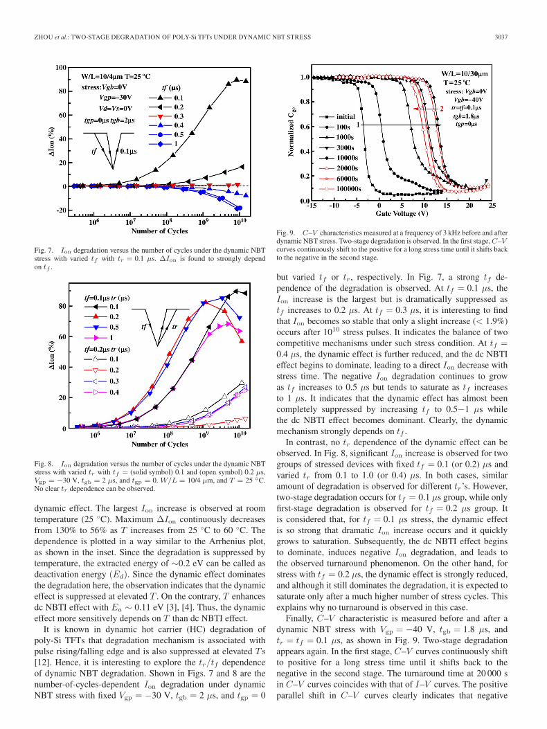
Fig. 7. Ion degradation versus the number of cycles under the dynamic NBTstress with varied tf with tr = 0.1 µs. ∆Ion is found to strongly dependon tf .
Fig. 8. Ion degradation versus the number of cycles under the dynamic NBTstress with varied tr with tf = (solid symbol) 0.1 and (open symbol) 0.2 µs,Vgp = −30 V, tgb = 2 µs, and tgp = 0. W/L = 10/4 µm, and T = 25 ◦C.No clear tr dependence can be observed.
dynamic effect. The largest Ion increase is observed at roomtemperature (25 ◦C). Maximum ∆Ion continuously decreasesfrom 130% to 56% as T increases from 25 ◦C to 60 ◦C. Thedependence is plotted in a way similar to the Arrhenius plot,as shown in the inset. Since the degradation is suppressed bytemperature, the extracted energy of ∼0.2 eV can be called asdeactivation energy (Ed). Since the dynamic effect dominatesthe degradation here, the observation indicates that the dynamiceffect is suppressed at elevated T . On the contrary, T enhancesdc NBTI effect with Ea ∼ 0.11 eV [3], [4]. Thus, the dynamiceffect more sensitively depends on T than dc NBTI effect.
It is known in dynamic hot carrier (HC) degradation ofpoly-Si TFTs that degradation mechanism is associated withpulse rising/falling edge and is also suppressed at elevated T s[12]. Hence, it is interesting to explore the tr/tf dependenceof dynamic NBT degradation. Shown in Figs. 7 and 8 are thenumber-of-cycles-dependent Ion degradation under dynamicNBT stress with fixed Vgp = −30 V, tgb = 2 µs, and tgp = 0
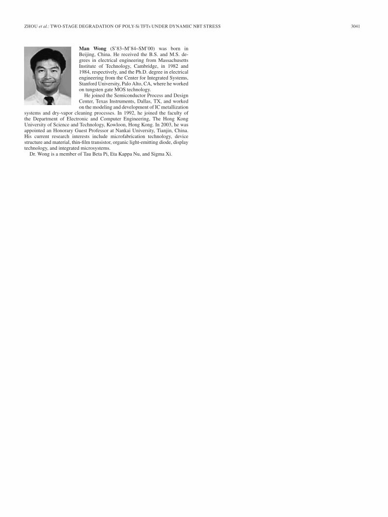
Fig. 9. C–V characteristics measured at a frequency of 3 kHz before and afterdynamic NBT stress. Two-stage degradation is observed. In the first stage, C–Vcurves continuously shift to the positive for a long stress time until it shifts backto the negative in the second stage.
but varied tf or tr, respectively. In Fig. 7, a strong tf de-pendence of the degradation is observed. At tf = 0.1 µs, theIon increase is the largest but is dramatically suppressed astf increases to 0.2 µs. At tf = 0.3 µs, it is interesting to findthat Ion becomes so stable that only a slight increase (< 1.9%)occurs after 1010 stress pulses. It indicates the balance of twocompetitive mechanisms under such stress condition. At tf =0.4 µs, the dynamic effect is further reduced, and the dc NBTIeffect begins to dominate, leading to a direct Ion decrease withstress time. The negative Ion degradation continues to growas tf increases to 0.5 µs but tends to saturate as tf increasesto 1 µs. It indicates that the dynamic effect has almost beencompletely suppressed by increasing tf to 0.5−1 µs whilethe dc NBTI effect becomes dominant. Clearly, the dynamicmechanism strongly depends on tf .
In contrast, no tr dependence of the dynamic effect can beobserved. In Fig. 8, significant Ion increase is observed for twogroups of stressed devices with fixed tf = 0.1 (or 0.2) µs andvaried tr from 0.1 to 1.0 (or 0.4) µs. In both cases, similaramount of degradation is observed for different tr’s. However,two-stage degradation occurs for tf = 0.1 µs group, while onlyfirst-stage degradation is observed for tf = 0.2 µs group. Itis considered that, for tf = 0.1 µs stress, the dynamic effectis so strong that dramatic Ion increase occurs and it quicklygrows to saturation. Subsequently, the dc NBTI effect beginsto dominate, induces negative Ion degradation, and leads tothe observed turnaround phenomenon. On the other hand, forstress with tf = 0.2 µs, the dynamic effect is strongly reduced,and although it still dominates the degradation, it is expected tosaturate only after a much higher number of stress cycles. Thisexplains why no turnaround is observed in this case.
Finally, C–V characteristic is measured before and after adynamic NBT stress with Vgp = −40 V, tgb = 1.8 µs, andtr = tf = 0.1 µs, as shown in Fig. 9. Two-stage degradationappears again. In the first stage, C–V curves continuously shiftto positive for a long stress time until it shifts back to thenegative in the second stage. The turnaround time at 20 000 sin C–V curves coincides with that of I–V curves. The positiveparallel shift in C–V curves clearly indicates that negative

3038 IEEE TRANSACTIONS ON ELECTRON DEVICES, VOL. 58, NO. 9, SEPTEMBER 2011
Fig. 10. Shown in (a) is the estimated increase in negative-charge density(−∆Qf ) and the grain-boundary trap density (∆Nt); here, Nt is the grain-boundary trap density. The comparison between the Vt shift extracted fromC–V and the Vth shift extracted from I–V curves is shown as the solid symbolin (b), and the open symbol shows the Vth shift calculated by using the Vth
model in [16].
fixed charges are generated during the first stage. As a result,channel inversion threshold voltage (Vt) increases, which isestimated as the Vg position where capacitance is one-thirdup from the minimum of the C–V curves [13]. It is noticedthat, in stressed C–V curves, the curve in Vg range below Vt
stretches, which can be attributed to the generation of interfacetraps near the source/drain region [14]. However, the stretch ismuch less significant than the positive/negative parallel shift inC–V . Since the C–V shift is dominated by charge generation∆Qf , it can be used to estimate ∆Qf roughly [15]: ∆Qf =Cox∆Vt/q, where Cox = 3.1 × 10⁻⁸ F/cm2 is the gate oxidecapacitance per unit area. Large amount of negative charges(∼3 × 1012 cm−2) is generated under dynamic NBT stress,as shown in Fig. 10(a). Similarly, positive charges generatedby dc NBTI in the second stage can be also estimated as∼5 × 1011 cm−2. Clearly, dynamic effect generates negativecharges much more efficiently than dc NBTI does for positivecharges, thus dominating the first degradation stage. It is untilthe dynamic effect tends to saturate after a long stress time thatthe dc NBT effect begins to dominate, leading to the turnaroundand the second-stage degradation.
In Fig. 10(b), the shifts of Vth and Vt are compared. Withno surprise, Vth and Vt degrade, following similar trend withstress time; however, ∆Vth deviates from ∆Vt. As has beenreported, the Vth of p-channel poly-Si TFTs is modeled as [16]Vth = Vt − H/3, where H is a GB barrier parameter relating toGB trap density Nt by H = q3N2
t d/8εsCoxkT , where εs is theSi permittivity and d is the inversion layer thickness. Thus, Nt
generation causes negative shift of Vth. By using the Levinsonmethod [17], Nt can be estimated from transfer curves, and∆Nt is shown in Fig. 10(a). For device degradation after a3000-s stress, ∆Vt is +15 V, as extracted from the C–V shift,while Nt generation (∼ 6.5 × 1011 cm−2) causes Vth negativeshift of −3.4 V. Thus, the total Vth shift should be +11.6 V,which is close to the experimental ∆Vth (+10.8 V) extractedfrom I–V . As shown in Fig. 10(b), the model well explains theobserved Vth shift before the turnaround. The mismatch after
Fig. 11. Possible negative-charge generation model. As the lateral electricalfield across the depletion region between the intrinsic channel and doped S/Dbecomes high enough, the impact ionization is induced under the dynamic NBTstress. Hot electrons leap over the surface potential barrier, break the ≡SiOHbonds, and form an interface state ≡Si∗ and a fixed charge OH−.
it could arise from Nt extraction errors for heavily stresseddevices. It may be attributed to the generation of interface traps,which was not taken into consideration in the extraction.
C. Negative-Charge Generation Model
Aside from the positive charge generation due to dc NBTImechanism, there must be a new mechanism accounting forthe large amount of negative-charge generation under dynamicNBT stress. A possible mechanism is tentatively proposed here.Previously, the effect of moisture on MOSFETs and TFTs hasbeen reported [18], [19]. Molecular H2O can penetrate SiO2
layer until it encounters a favorable site where it reacts to forman immobile Si hydroxyl group [20], i.e., H2O+ ≡SiOSi≡↔≡Si−OH + OH−Si≡. In this paper, LPCVD low-temperatureoxide is used as the gate oxide, which is typical for low-temperature poly-Si TFTs but could be sensitive to moistureexposure. Hence, we assume that plenty of ≡SiOH groups existin the vicinity of the gate-oxide/channel interface. A possiblenegative-charge generation model is shown in Fig. 11. As thelateral electrical field across the depletion region between theintrinsic channel and doped S/D becomes high enough,the impact ionization is induced under the dynamic NBT stress.Hot electrons leap over the surface potential barrier, break the≡SiOH bonds with disassociation energy of ∼1.2 eV [21],and form an interface state ≡Si∗ and a fixed charge OH− ase−(hot)+ ≡SiOH →≡Si∗ + OH−. Hence, fixed charges OH−
in the gate oxide or interface are generated.A depletion region is formed between the intrinsic channel
and the highly doped source/drain. In the falling edge ofdynamic NBT stress, where Vg quickly switches from zero tonegative, holes cannot be supplied to the channel immediately,and the depletion region still exists. During the steep pulsetransition, the impedance of gate insulator (1/j2πfCox) issmall. The transient Vg would drop mainly across the channeland the depletion region. The electrical field across the regionincreases with increasing Vg . It could become high enoughto induce impact ionization. The transient electric field andcurrent density from drain to channel, noted as Ex and Jx, re-spectively, during tf = 0.1 µs and Vgp = −30 V are simulatedby SILVACO, as shown in Fig. 11. The simulation spot is at

ZHOU et al.: TWO-STAGE DEGRADATION OF POLY-Si TFTs UNDER DYNAMIC NBT STRESS 3039
Fig. 12. Transient electric field and current density from drain to channel (Ex
and Jx) are simulated by SILVACO during the gate voltage switches from 0 to−30 V in 0.1 µs. The Ex dependence on the falling time for a fixed Vgp =−30 V and also the Ex dependence on pulse amplitude Vgp for a fixed tf =0.1 µs are plotted in the inset. Ex is estimated in a point in time correspondingto the peak Ex occurrence in the falling edge. The simulation spot is at thechannel/drain edge in the depletion region.
the channel/drain edge in the depletion region. Ex is found toincrease to a high field (∼2.2 × 10⁴ V/cm). Simultaneously, alateral current Jx is found following the same direction of Ex.Carriers exposed to the high field may become HCs throughimpact ionization. Approaching the end of the falling edge,channel hole concentration rises with Vg , the depletion regionshrinks, and the Ex decreases. During rising edge, channelinversion hole concentration is quite high, and no depletionregion between the channel and S/D can be formed. That is whythe dynamic effect does not depend on tr. The Ex dependenceon pulse amplitude and falling time is also simulated, as shownin the inset of Fig. 12. Ex is extracted at a transient of tfcorresponding to the peak Ex. Ex is the largest at tf = 0.1 µsand continuously decreases as tf increases from 0.1 to 0.5 µs.At fixed tf = 0.1 µs, Ex is enhanced as Vgp increases from −20to −40 V. Thus, at higher Vgp and shorter tf , impact ionizationis easier to occur, and more dynamic effects would be intro-duced, which is in accord with our experimental observations.Impact ionization coefficient decreases at higher temperatures[22], while avalanche-generated electron-hole pairs exponen-tially depend on the coefficient. It should be the reason why thedynamic effect decreases as temperature increases and is moresensitive to the temperature than dc NBTI effect, as observedin Fig. 6.
In the proposed negative-charge generation model, the im-pact ionization is near the S/D, which would result in nonuni-form degradation along the channel. To analyze this effect,the degradation under dynamic NBT stress on devices withdifferent L values is investigated. Shown in Fig. 13 is the Ion
degradation dependent on stress time of devices with L variedfrom 30 to 2 µm. The dynamic NBT stress with Vgp = −40 V,tgb = 2 µs, and tr = tf = 0.1 µs is applied. A significant two-stage degradation is observed. Before the turnaround point,dynamic effect dominates the degradation, and ∆Ion increasesas L decreases from 30 to 2 µm, as shown in the inset. It isnot surprising since shorter L device should be more sensitive
Fig. 13. Ion degradation under dynamic NBT stress on devices with differentL values. Vgp = −40 V, tr = tf = 0.1 µs, tgb = 2 µs, tgp = 0, and T =25 ◦C. The Ion degradation dependence on L after a 100-s stress is plotted inthe inset.
to the damage near the source-and-drain region. Furthermore,the turnaround is found to occur earlier as L decreases, asshown at the arrow. The turnaround of the degradation underdynamic NBT stress is considered to be the result of thecombination of two competitive mechanisms: dynamic effectand dc NBTI effect. According to the proposed model, dynamicNBT-induced degradation should be higher and saturate earlierfor shorter L devices. Moreover, the dc NBTI degradation isseverer in shorter L devices [23]. Hence, before the dynamic-effect-induced Ion increase reaches a higher level, the dc NBTIeffect has dominated the degradation and thus leads to theearlier turnaround and also the lower overall Ion increase forshorter L devices.
As mentioned in Section III-A, a hump appears in the sub-threshold region during the first degradation stage and finallydisappears after a long time stress (see Fig. 2). Hump phe-nomenon has been reported in poly-Si TFTs and MOSFETs[18], [24], [25]. It is attributed to the presence of parallelparasitic transistors located at two channel edges at the channelwidth side, which have locally reduced Vth due to electric fieldcrowding effect. Device characteristic is the summation of thechannel device and two parallel parasitic edge devices [24].No hump exists in the initial I–V characteristics of our TFTs,indicating that the Vth of the parasitic edge device is the sameas that of the channel device. However, the dynamic NBT stressinduces subthreshold hump and can be understood based on ourdegradation model. As the dynamic NBT stress is applied, alsodue to electric field crowding effect, the dynamic-effect-relatedimpact ionization should occur first in edge devices or beseverer than that of the channel device. Hence, a Vth differenceis introduced between the channel and edge devices, with theedge devices having somewhat lower Vth due to more negative-charge generation therein. Thus, a hump is developed in thesubthreshold region. As stress continues, charge generation be-comes uniform possibly due to the saturation of dynamic effect;thus, the hump disappears before the second-stage degradationoccurs.

3040 IEEE TRANSACTIONS ON ELECTRON DEVICES, VOL. 58, NO. 9, SEPTEMBER 2011
IV. CONCLUSION
Degradation of p-channel poly-Si TFTs under dynamic NBTstress has been studied. A two-stage degradation is observed.The dynamic effect and dc NBTI effect are thought to beresponsible for this instability. After analyzing the dynamiceffect, we found that it is enhanced by the pulse amplitude andstrongly depends on the pulse falling time. Negative chargesare observed to be generated under the dynamic NBT stress. Itis considered that hot electrons educed by the impact ionizationbreak the bond of ≡SiOH and, then, the negative ions (OH−)are generated in the gate oxide, which shift the Vth to positive.The dynamic effect eventually saturates after a long time stress,and then, the dc NBTI effect dominates the device degradation.
REFERENCES
[1] N. D. Yang and J. R. Ayres, “Negative gate bias instability in poly-crystalline silicon TFTs,” IEEE Trans. Electron Devices, vol. 42, no. 9,pp. 1623–1627, Sep. 1995.
[2] C. Y. Chen, J. W. Lee, S. D. Wang, M. S. Shieh, P. H. Lee, W. C. Chen,H. Y. Lin, K. L. Yeh, and T. F. Lei, “Negative bias temperature instabil-ity in low-temperature polycrystalline silicon thin-film transistors,” IEEETrans. Electron Devices, vol. 53, no. 12, pp. 2993–3000, Dec. 2006.
[3] C. Hu, M. Wang, M. Zhang, B. Zhang, and M. Wong, “Degradationof solution based metal induced laterally crystallized p-type poly-SiTFTs under DC bias stresses,” in Proc. Int. Rel. Phys. Symp., 2008,pp. 363–367.
[4] C. Hu, M. Wang, B. Zhang, and M. Wong, “Negative bias temperatureinstability dominated degradation of metal-induced laterally crystallizedp-type polycrystalline silicon thin-film transistors,” IEEE Trans. ElectronDevices, vol. 56, no. 4, pp. 587–594, Apr. 2009.
[5] G. Chen, M. F. Li, C. H. Ang, J. Z. Zheng, and D. L. Kwong, “Dy-namic NBTI of p-MOS transistors and its impact on MOSFET scaling,”IEEE Electron Device Lett., vol. 23, no. 12, pp. 734–736, Dec. 2002.
[6] M. Ershov, S. Saxena, H. Karbasi, S. Winters, S. Minehane, and J.Lindley,R., Clifton, P., Redford, M., Shibkov, A. Babcock, “Dynamic recov-ery of negative bias temperature instability in p-type metal–oxide–semiconductor field-effect transistors,” Appl. Phys. Lett., vol. 83, no. 8,pp. 1647–1649, Aug. 2003.
[7] S. S. Tan, T. P. Chen, and L. Chan, “Dynamic NBTI lifetime modelfor inverter-like waveform,” Microelectron. Reliab., vol. 45, no. 7/8,pp. 1115–1118, Jul./Aug. 2005.
[8] J. C. Liao, Y. K. Fang, C. H. Kao, and C. Y. Cheng, “Dynamic negativebias temperature instability (NBTI) of low-temperature polycrystallinesilicon (LTPS) thin-film transistors,” IEEE Electron Device Lett., vol. 29,no. 5, pp. 477–479, May 2008.
[9] C. F. Huang, H. C. Sun, P. S. Kuo, Y. T. Chen, C. W. Liu, Y. J. Hsu, andJ. S. Chen, “Dynamic bias temperature instability of p-channel polycrys-talline silicon thin-film transistors,” in Proc. 16th IEEE Int. Symp. Phys.Failure Anal. Integr. Circuits, 2009, pp. 158–162.
[10] J. Zhou, M. Wang, and M. Wong, “Instability of p-channel poly-Sithin-film transistors under dynamic negative bias temperature stress,” inProc. 17th IEEE Int. Symp. Phys. Failure Anal. Integr. Circuits, 2010,pp. 317–320.
[11] B. Zhang, Z. Meng, S. Zhao, M. Wong, and H.-S. Kwok, “Polysil-icon thin-film transistors with uniform and reliable performance us-ing solution-based metal-induced crystallization,” IEEE Trans. ElectronDevices, vol. 54, no. 5, pp. 1244–1248, May 2007.
[12] Y. Uraoka, H. Yano, T. Hatayama, and T. Fuyuki, “Comprehensive studyon reliability of low-temperature poly-Si thin-film transistors under dy-namic complimentary metal-oxide semiconductor operations,” Jpn. J.Appl. Phys., vol. 41, no. 4B, pp. 2414–2418, Apr. 2002.
[13] M. D. Jacunski, M. S. Shur, and M. Hack, “Threshold voltage, field effectmobility, and gate-to-channel capacitance in polysilicon TFTs,” IEEETrans. Electron Devices, vol. 43, no. 9, pp. 1433–1440, Sep. 1996.
[14] S.-C. Huang, Y.-H. Kao, and Y.-H. Tai, “Study on electrical degradationof p-type low-temperature polycrystalline silicon thin film transistor withC–V measurement analysis,” Thin Solid Films, vol. 515, no. 3, pp. 1206–1209, Nov. 2006.
[15] M. Wang and M. Wong, “An effective channel mobility based analyticalon-current model for polycrystalline silicon thin film transistor,” IEEETrans. Electron Devices, vol. 54, no. 4, pp. 869–874, Apr. 2007.
[16] Y. Zhou, M. Wang, D. Zhou, and M. Wong, “An analytical expression forthreshold voltage of polycrystalline-silicon thin-film transistors,” IEEEElectron Device Lett., vol. 31, no. 8, pp. 815–817, Aug. 2010.
[17] J. Levinson, F. R. Shepherd, P. J. Scanlon, W. D. Westwood, G. Este, andM. Rider, “Conductivity behavior in polycrystalline semiconductor thinfilm transistors,” J. Appl. Phys., vol. 53, no. 2, pp. 1193–1202, Feb. 1982.
[18] N. D. Young and A. Gill, “Water-related instability in TFTs formed usingdeposited gate oxides,” Semicond. Sci. Technol., vol. 7, no. 8, pp. 1103–1108, Aug. 1992.
[19] K. Sasada, M. Arimoto, H. Nagasawa, A. Nishida, H. Aoe, T. Dan,S. Fujiwara, Y. Matsushita, and K. Yodoshi, “The influence of SIN filmson negative bias temperature instability and characteristics in MOSFETs,”in Proc. IEEE Int. Conf. Microelectron. Test Struct., 1998, vol. 11,pp. 207–210.
[20] R. H. Doremus, “Oxidation of silicon by water and oxygen and diffusionin fused silica,” J. Phys. Chem., vol. 80, no. 16, pp. 1773–1775, 1976.
[21] M. D. Allendorf, C. F. Melius, P. Ho, and M. R. Zachariah, “Theoreti-cal study of the thermochemistry of molecules in the Si–O–H system,”J. Phys. Chem., vol. 99, no. 41, pp. 15 285–15 293, 1995.
[22] M. Ershov and V. Ryzhii, “Temperature dependence of the electron impactionization coefficient in silicon,” Semicond. Sci. Technol., vol. 10, no. 2,pp. 138–142, Feb. 1995.
[23] T. Yamamoto, K. Uwasawa, and T. Mogami, “Bias temperature instabil-ity in scaled p+ polysilicon gate p-MOSFETs,” IEEE Trans. ElectronDevices, vol. 46, no. 5, pp. 921–926, May 1999.
[24] A. Valletta, P. Gaucci, L. Mariucci, G. Fortunato, and F. Templier,“‘Hump’ characteristics and edge effects in polysilicon thin film tran-sistors,” J. Appl. Phys., vol. 104, no. 12, pp. 124511.1–124511.6,Dec. 2008.
[25] N. Shigyo, S. Fukuda, T. Wada, K. Hieda, T. Hamamoto, H. Watanabe,K. Sunouchi, and H. Tango, “Three-dimensional analysis of subthresholdswing and transconductance for fully recessed oxide (trench) isolated1/4-µm-width MOSFETs,” IEEE Trans. Electron Devices, vol. 35, no. 7,pp. 945–951, Jul. 1988.
Jie Zhou was born in Nantong, China, in 1986. Shereceived the B.S. degree in microelectronics fromSoochow University, Suzhou, China, in 2008, whereshe is currently working toward the M.S. degree inthe Department of Microelectronics.
Her current research work is about the NBTI ofp-channel poly-Si TFTs.
Mingxiang Wang (M’07–SM’09) received the B.S.degree in physics and the Ph.D. degree in condensedmatter physics from Nanjing University, Nanjing,China, in 1993 and 1998, respectively.
From 1998 to 2001, he was a Postdoctoral Re-search Associate with the Department of Electri-cal and Electronic Engineering, The Hong KongUniversity of Science and Technology, Kowloon,Hong Kong. He joined Semiconductor Manufactur-ing International Corporation, Shanghai, China, as aMember of the technical staff in process reliability
engineering. He is currently with the Department of Microelectronics, SoochowUniversity, Suzhou, China. His research interests include thin-film materialsand devices, semiconductor device physics, and device reliability.
ZHOU et al.: TWO-STAGE DEGRADATION OF POLY-Si TFTs UNDER DYNAMIC NBT STRESS 3041
Man Wong (S’83–M’84–SM’00) was born inBeijing, China. He received the B.S. and M.S. de-grees in electrical engineering from MassachusettsInstitute of Technology, Cambridge, in 1982 and1984, respectively, and the Ph.D. degree in electricalengineering from the Center for Integrated Systems,Stanford University, Palo Alto, CA, where he workedon tungsten gate MOS technology.
He joined the Semiconductor Process and DesignCenter, Texas Instruments, Dallas, TX, and workedon the modeling and development of IC metallization
systems and dry-vapor cleaning processes. In 1992, he joined the faculty ofthe Department of Electronic and Computer Engineering, The Hong KongUniversity of Science and Technology, Kowloon, Hong Kong. In 2003, he wasappointed an Honorary Guest Professor at Nankai University, Tianjin, China.His current research interests include microfabrication technology, devicestructure and material, thin-film transistor, organic light-emitting diode, displaytechnology, and integrated microsystems.
Dr. Wong is a member of Tau Beta Pi, Eta Kappa Nu, and Sigma Xi.


![Synthesis and degradation of poly (alkyl [alpha]-cyanoacrylates) · 2012-11-23 · POLY(ALKYL a-CYANOACRYLATES) 261 The mononiers obtained after redistillatioil were found to have](https://img.pdfslide.us/doc/110x75/5f1fb66ae2851b644e6140c0/synthesis-and-degradation-of-poly-alkyl-alpha-cyanoacrylates-2012-11-23-polyalkyl.jpg)