Embed Size (px)
Citation preview

Full Terms & Conditions of access and use can be found athttp://www.tandfonline.com/action/journalInformation?journalCode=tetl20
Download by: [Ryerson University Library] Date: 01 November 2016, At: 09:54
International Journal of Electronics Letters
ISSN: 2168-1724 (Print) 2168-1732 (Online) Journal homepage: http://www.tandfonline.com/loi/tetl20
Two-Stage Class-AB OTA with Enhanced DC-Gainand Slew Rate
Seyed Mahmoud Anisheh & Hossein Shamsi
To cite this article: Seyed Mahmoud Anisheh & Hossein Shamsi (2016): Two-Stage Class-ABOTA with Enhanced DC-Gain and Slew Rate, International Journal of Electronics Letters, DOI:10.1080/21681724.2016.1253780
To link to this article: http://dx.doi.org/10.1080/21681724.2016.1253780
Accepted author version posted online: 27Oct 2016.
Submit your article to this journal
Article views: 2
View related articles
View Crossmark data

1
Publisher :Taylor & Francis
Journal :International Journal of Electronics Letters
DOI :10.1080/21681724.2016.1253780
Two-Stage Class-AB OTA with Enhanced DC-Gain and Slew Rate
Seyed Mahmoud Anisheh, Hossein Shamsi*
Faculty of Electrical Engineering, K. N. Toosi University of Technology *Corresponding author, Email: [email protected]
Abstract This letter proposes a new two-stage class-AB operational trans-conductance amplifier (OTA). In this OTA, the characteristics of class-AB are applied in both of the stages. By increasing the effective trans-conductance of the first stage, DC-gain is improved. Nonlinear current mirror boosts the current of the second stage; Therefore, Slew Rate (SR) is increased. In order to verify the performance of the proposed OTA, some simulations are carried out in a 0.18μm CMOS process in which the supply voltage is 1.8 V. The simulation results indicate 21 dB enhancement in DC-gain and 2.7 times improvement in SR compared to its conventional counterpart. The post-layout and Monte Carlo (MC) simulations show the proposed OTA has better performance than the state of the art designs. Keywords: Operational Trans-conductance Amplifier; Class-AB OTAs; DC-Gain; Slew Rate; Post-layout Simulation.
1. Introduction
*Corresponding author, Email: [email protected]

2
Nowadays, due to increase in applications of switched-capacitor, sample-and-hold circuits, and data converters in electronic circuits, serving of OTAs is necessary as one of the main usable part in their circuit configurations (Akbari, Biabanifarda, Asadi, & Yagoub, 2014; Akbari, Biabanifarda, Asadi, & Yagoub, 2015). The OTAs should have high DC-gain, slew rate (SR), and unity-gain bandwidth (UGBW) while operating with low-voltage and low static power. Achieving these specifications are not viable using class-A OTAs. This is mainly due to the fact that the increasing of SR and UGBW would lead to increase power dissipation, considerably. Some techniques have been proposed in the literature for low-power OTAs. One of these techniques is based on bulk-driven method (Ferreira, Pimenta, & Moreno, 2007; Raikos & Vlassis, 2011; Ferreira & Sonkusale, 2014). The main disadvantage of a bulk-driven MOS device in CMOS technologies is that bulk-source trans-conductance is smaller than the gate-source trans-conductance and may not be sufficient in some cases. Class-AB OTAs can be considered as a better solution for the realization of the above specifications. Several class-AB OTAs have been suggested in the literatures (Callewaert & Sansen, 1990; Galan, López-Martín, Carvajal, Ramírez-Angulo, & Rubia-Marcos, 2007; Noormohammadi & Hajsadeghi, 2012; Liu & Yang, 2006; Baharudin, Jambek, & Ismail, 2014). A class-AB OTA has been introduced to increase tail current when large input signals are applied (Callewaert & Sansen, 1990). However, due to the extra circuitry, the power consumption has increased drastically. An adaptive-biasing circuit (ABC) based class-AB OTA has been proposed that is suitable for low-voltage operation (Galan, López-Martín, Carvajal, Ramírez-Angulo, & Rubia-Marcos, 2007). The main drawback of this technique is its poor performance in terms of output noise. A class-AB output stage OTA using current boosting method has been proposed which enhances both of the SR and UGBW parameters (Noormohammadi & Hajsadeghi, 2012). This method suffers from high static power consumption due to class-A operation of the input stage. A low-voltage, low-power class-AB OTA has been proposed, which is based on the current mirror OTA topology and positive feedback (Liu & Yang, 2006). However, stability of the OTA may encounter difficulties due to variations of process and environmental parameters. A two-stage OTA has been proposed which has high DC-gain (Baharudin, Jambek, & Ismail, 2014). However, SR has not been increased significantly. In this letter, a new two-stage class-AB OTA has been introduced. The results indicate the superiority of the proposed technique in terms of DC-gain and SR compared to the conventional OTA. In Section 2, the proposed OTA is described. The performance evaluations of the OTA and comparison results are presented in Section 3. Finally, Section 4 concludes the letter.
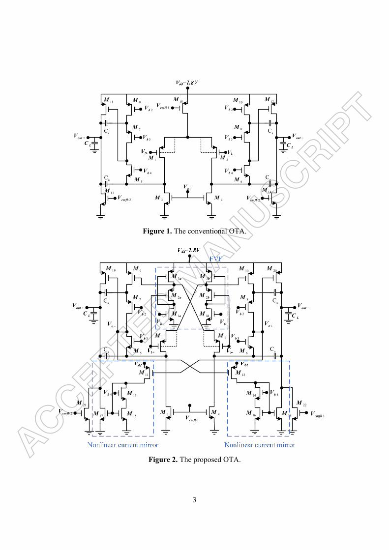
2. Proposed OTA Figure 1 shows the conventional two-stage OTA that utilizes hybrid-cascode compensation technique (Yavari, 2005). Also, Figure 2 shows the circuit configuration of the proposed OTA. The common-mode feedback (CMFB) circuit is shown in Figure 3. The differential pair in the first stage consists of two matched transistors 1M and 2M
which are biased by an ABC. Under the conditions in which the differential input is not applied, small quiescent currents would be flowed through 1M and 2M . However, this
current would be boosted when the differential input voltage is sensed by ABC. Based on the aforementioned discussion, the proposed circuit can be classified as a class-AB OTA.
3
1M 2M
3M 4M
5M 6M
7M 8M
9M 10M15M
3bVLC
2bV
1bV
4bV
2bV
3bV
4bV
2cmfbV2cmfbV
11M 12M
14M
1cmfbV
−outV+outV sC sC
aC aC
13M
LC
Figure 1. The conventional OTA.
1M 2M
3M 4M
5M 6M
7M 8M
9M 10M
2bVLC
3bV
1bV2bV
3bV
2cmfbV
19M 20M
1cmfbV
−outV+outV sC sC
aC aC
−oV +oVLC
4bV
2cmfbV
4bV
1aM
17M
13M 14M
15M 16M
12M11M
21M 22M
1bV
18M
1bM
2aM 2bM
3aM 3bM
Figure 2. The proposed OTA.

4
1M 2M
3M 4M 5M 6M
7M
8M
+oV −oV
Figure 3. Common-mode feedback (CMFB) circuit
The adopted ABC is composed of a modified version of the source follower named as flipped voltage follower (FVF) (Carvajal, Ramirez-Angulo, Torralba, Galan, Carlosena, & Chavero, 2005; Guo, Ho, Kwong, & Leung, 2015; Kim & Lee, 2013). The FVF consists of transistors 2 2,a bM M and 3 3,a bM M , in which 1 1,a bM M act as current
sources that provide quiescent current equal to BI . By neglecting second-order effects,
the source-gate voltage of 2aM is given by
2 , 22
2
(W/ L)B
SG a th p ap ox a
IV V
C= + (1)
where ,pthV is the threshold voltage of PMOS transistor. By considering
9 2 1,G SG a CMiV V V= + where 1CMiV is the input common-mode voltage of the first stage, the
current through 9M can be obtained. The source-gate voltage of 2M is given by
2 2 .SG SG aV V= therefore, the current through 2M is calculated. The voltage OV − is
determined by CMFB1; hence, the current through 19M is found.
By applying the input signal, the current flowing in one of the differential pair transistors increases. For example, consider a condition in which iV + and iV − increases and
decreases, respectively. Upon this, the source voltages of 1M and 2M are decreased and
increased, and their drain currents would be decreased and increased, respectively. Source of 2M is connected to the drain of 3aM and to the gate of 9M . Also, Source of
1M is connected to the drain of 3bM and to the gate of 10M . This architecture realize the
class-AB operation for the active load transistors 9M and 10M that are associated with
the common-gate transistors 5M and 6M . By applying the input signal to the OTA, this
5
signal would also appear at the gate-source of 9M and 10M by means of FVF. Therefore,
the trans-conductance of the input stage is increased from 1,2mg to 1,2 9,10meff m mg g g= +
which enhance the DC-gain. Increasing the input stage trans-conductance can also reduce the total input-referred noise voltage as follows:
2
1,a2 2 31,prop ,2 2
4 4m mmni ni conv
meff meff meff
g ggV kT V kT
g g g
≈ × + × + ×
(2)
where 2,ni convV denotes the total input-referred noise voltage of the conventional OTA.
FVF-based nonlinear current mirrors have been used for the output active loads that are composed of transistor sets 11 13 15 17( , , , )M M M M and 12 14 16 18( , , , )M M M M . The gates
of 11M and 12M are connected to the nodes oV + and oV − , respectively. The transistors
15M and 16M are biased close to the triode region so that their drain-source voltages
would be a bit higher than DS,satV . Consider a condition in which input voltages iV + and
iV − are increased and decreased, respectively. Then, voltages of the nodes oV − and oV +
are decreased and increased, respectively. The current through 12M increases by
decreasing the voltage of the node oV − . Then the gate-source voltage of 14M and the
drain-source voltage of 16M are increased and decreased, respectively. Thus 16M is
pushed into the triode region. As a result, a large voltage variation is produced across the gate-source of 16M that can be expressed as below:
16 16 16 , 16( ).GS th n DSI V V V= − (3)
where 16 16(W/ L)n oxC= and ,th nV is the threshold voltage of NMOS transistor.
A large gate-source voltage variation of 16M would boost the current of the active load
18M . This current can be obtained by equation (4) as long as it remains in saturation
region. 22
121 1 ,
1818
16 16
2 22
idDD meff o CMO th n
DS
VV g R V V
IV
− − − =
×
(4)
where 1CMOV is the common-mode output voltage of the first stage, and 1oR denotes the
resistance of node oV − . From (4) it is clear that for a large idV the output current
increases with 4
idV , that would enhance the current boosting provided by the Class-AB,
quadratically.
3. Simulation Results In order to verify the performance of the proposed OTA compared to the conventional one, some simulations are carried out. Both of the competitors are designed in a 0.18 μm CMOS process with 1.8V supply voltage. Supply voltage, load capacitor, phase margin,

6
and power dissipation are identical for both OTAs. Currents allocations to MOSFETs used in the proposed OTA are reported in Table 1. Gm versus differential input voltage for both of the proposed and conventional OTAs are demonstrated in Figure 4. The results show that the Gm of the proposed OTA is higher than the conventional OTA. The Bode diagrams of the competitors are shown in Figure 5, indicating 21 dB DC-gain improvement in schematic level simulation. UGBW and phase margin of the proposed
OTA are 270 MHz and o65 , respectively. Complete OTA specifications along with a comparison to the conventional OTA are summarized in Table 2. As seen from the results, SR of the proposed OTA has been enhanced 2.7 times compared to its conventional counterpart. Moreover, the total input-referred noise voltage of the proposed OTA is smaller than the conventional design. The physical layout of the both OTAs is shown in Figure 6. As a drawback, the layout area of the proposed OTA is increased by the factor of 1.2 compared to the conventional one. This is mainly due to larger compensating capacitors in the proposed OTA for achieving equal phase margin compared to conventional OTA. Figure 7 shows the Monte Carlo (MC) histograms of the proposed OTA comprising of 10000-run simulations, and the results are summarized in Table 3. The results show that the variations in OTA specifications are relatively low. Post-layout simulation results are compared with some other methods in Table 4. The proposed OTA shows the small value for layout area compared to the most existing methods. Moreover, the proposed OTA has the highest DC-gain, at least 19 dB more than the other solutions. In order to compare the other performance parameters, the traditional couple of figure of merits in (5), (6) which for a given load show a trade-off between speed performance and total bias current ( TI ) are utilized (Grasso, Palumbo, & Pennisi,
2006; Grasso, Palumbo, & Pennisi, 2007). . L
ST
UGBW CFOM
I=
(5) SR . L
LT
CFOM
I=
(6) As can be seen from Table 4, the proposed OTA has proper values for both of FOMs and FOML.
Table 1. Currents allocations to MOSFETs.
Device Current Value (µA)
1M 128
1aM 114
9M 214
11M 98
19M 255

7
Figure 4. Gm versus differential input voltage for both OTAs.

8
Figure 5. Bode diagrams of the OTAs.
Table 2. Specifications of the proposed and conventional OTAs.
Specification
Conventional OTA Proposed OTA
TT( 27C) FF( 40− C) SS( 90C) TT( 27C) FF( 40− C) SS( 90C)
Technology 0.18μm 0.18μm 0.18μm 0.18μm 0.18μm 0.18μm
Supply Voltage 1.8V 1.8V 1.8V 1.8V 1.8V 1.8V
DC-Gain (dB) 74 69 71 95 86 96 Input-Referred Noise@100kHz
(μV/ Hz) 0.55 0.44 0.95 0.29 0.24 0.35
Layout Area 131μm×142μm 131μm×142μm 131μm×142μm 131μm×164μm 131μm×164μm 131μm×164μm
Output Voltage Swing (peak to
peak) (V) 2.8 2.8 2.8 2.8 2.8 2.8
Phase Margin () 68 64 78 65 63 67
Power Dissipation (mW)
2.9 4.3 1.8 2.9 3.9 2.1
Slew Rate (V/μs) 221 398 120 595 776 399
UGBW (MHz) 220 368 91 270 390 180 CL (pF) 1 1 1 1 1 1

9
(a) (b)
Figure 6. Physical layout of (a) the conventional and (b) proposed OTAs.
(a) (b)
(c) (d)

10
(e)
Figure 7. Histogram of Monte Carlo Simulation. (a) DC Gain, (b) Power Dissipation, (c)
Phase Margin, (d) UGBW, (e) SR.
Table 3. The Monte Carlo Analysis of the Proposed OTA.
Specification Mean Value Standard Deviation DC Gain (dB) 94.1 1.2
Power Dissipation (mW) 2.9 0.079
Phase Margin () 66.7 2.1
UGBW (MHz) 265.1 22 Slew Rate (V/μs) 599 58
Table 4. Performance Comparison of the Proposed OTA and the Existing Methods.
This work
Yavari. (2005)
Ferreira, et al.
(2007)
Raikos, et al.
(2011)
Ferreira, et al.
(2014)
Galan, et al.
(2007)
Baharudin, et al.
(2014) b
Technology 0.18μm 0.18μm 0.35μm 0.18μm 0.13μm 0.5μm 0.13μm
Supply Voltage (V) 1.8 1.8 0.6 1 0.25 1 2.5 DC-Gain (dB) 93 72 69 64 60 30 74 Input-Reffered Noise@100kHz
(μv/ Hz) 0.31 0.58 -- -- -- 144 --
Layout Area (mm2) 0.021 0.018 0.060 0.063 0.083 0.011 -- Differential Output 2.8 2.8 -- -- -- -- 2.4

11
Swing (peak to peak) (V)
Phase Margin (degree)
65 66 65 45 53 90 62
Power Dissipation (mW)
3 3 0.00054 0.13 0.000018 0.08 1.3
Slew Rate (V/μs) 494 190 0.015 0.7 0.0007 0.35 47.9 UGBW (MHz) 216 177 0.011 2 0.002 0.2 0.02
Loading Capacitance (pF)
1 1 15 1 15 80 3
Operating Modea SI SI SUB, BD
SI, BD SUB, BD
SI SI
S
MHz.pFFOM =
mA 135 111 183 15 417 200 0.115
L
V.pFFOM =
μs.mA 309 119 250 5 146 350 276
aSUB: subthresold; BD: bulk driven; SI: strong inversion. bOnly Schematic level simulation
4. Conclusion
In this letter a new two-stage class-AB OTA in a 0.18 μm CMOS process with a 1.8 V
supply voltage has been presented. The proposed OTA was based on the simultaneous application of class-AB operation in both of the stages. In order to evaluate the effectiveness of the proposed method, several simulation scenarios have been performed. The results indicated the superiority of the proposed OTA in terms of DC-gain and SR compared to the conventional OTA with the cost of a little increase in the layout area. References Akbari, M., Biabanifarda, S., Asadi, S., & Yagoub, M. C. E. (2014). Design and analysis of DC gain and transconductance boosted recycling folded cascode OTA. AEU-International Journal of Electronics and Communications, 68(11), 1047-1052. doi:10.1016/j.aeue.2014.05.007 Akbari, M., Biabanifarda, S., Asadi, S., & Yagoub, M. C. E. (2015). High Rerformance Folded Cascode OTA Using Positive Feedback and Recycling Structure. Analog Integrated Circuits and Signal Processing, 82(1), 217-227. doi:10.1007/s10470-014-0464-0 Ferreira, L. H. C., Pimenta, T. C., & Moreno, R. L. (2007). An ultra-low-voltage ultra-low-power CMOS Miller OTA with rail-to-rail input/output swing. IEEE Trans. Circuits Syst. II, Exp. Briefs, 54(10), 843–847. doi: 10.1109/TCSII.2007.902216 Raikos, G., & Vlassis, S. (2011). Low-voltage bulk-driven input stage with improved transconductance. Int. J. Circuit Theor, 39(3), 327–339. doi:10.1002/cta.637

12
Ferreira, L. H. C., & Sonkusale, S. R. (2014). A 60-dB gain OTA operating at 0.25-V power supply in 130-nm digital CMOS process. IEEE Trans. Circuits Syst. I, Reg. Papers, 61(6), 1609-1617. doi: 10.1109/TCSI.2013.2289413 Callewaert, L. G. A., & Sansen, W. M. C. (1990). Class AB CMOS amplifiers with high efficiency. IEEE J. Solid-State Circuits, 25(3), 684–691. doi:10.1109/4.102661 Galan, J. A., López-Martín, A. J., Carvajal, R. G., Ramírez-Angulo, J., & Rubia-Marcos, C. (2007). Super class-AB OTAs with adaptive biasing and dynamic output current scaling. IEEE Transactions on Circuits and Systems I: Regular Papers, 54(3), 449-457. doi:10.1109/TCSI.2006.887639 Noormohammadi, M., Lazarjan., V-K., & Hajsadeghi, K. (2012). New operational transconductance amplifiers using current boosting. International Midwest Symposium on Circuits and Systems (pp. 109–112). doi:10.1109/MWSCAS.2012.6291969 Liu, A., & Yang, H. (2006). Low voltage low power class-AB OTA with negative resistance load. International Conference on Communications, Circuits and Systems Proceedings (pp. 2251 – 2254). doi:10.1109/ICCCAS.2006.285126 Baharudin, S. N. S., Jambek, A. B., & Ismail, R. C. (2014). Design and Analysis of a Two-Stage OTA for Sensor Interface Circuit. IEEE Symposium on Computer Applications & Industrial Electronics (ISCAIE) (pp. 88-92). doi:10.1109/ISCAIE.2014.7010215 Yavari, M. (2005). Hybrid cascode compensation for two-stage CMOS op-amps. IEICE trans. Electronics, 88(6), 1161-1165. doi:10.1093/ietele/e88-c.6.1161 Carvajal, R. G., Ramirez-Angulo, J., Torralba, A., Galan, J. A .G., Carlosena, A., & Chavero, F. M. (2005). The Flipped Voltage Follower: A Useful Cell for Low-Voltage Low-Power Circuit Design. IEEE Transactions on Circuits and Systems I: Regular Papers., 52(7), 1276 – 1291. doi:10.1109/TCSI.2005.851387 Guo, J., Ho, M., Kwong, K. Y., & Leung, K. N. (2015). Power-area-efficient transient-improved capacitor-free FVF-LDO with digital detecting technique. Electronics Letters, 51(1), 94–96. doi:10.1049/el.2014.3330 Kim, Y-I., & Lee, S-S. (2013). A capacitorless LDO regulator with fast feedback technique and low-quiescent current error amplifier. IEEE Trans. Circuits Syst. II, Exp. Briefs, 60(6), 326-330. doi:10.1109/TCSII.2013.2258250 Grasso, A. D., Palumbo, G., & Pennisi, S. (2006). Three-stage CMOS OTA for large capacitive loads with efficient frequency compensation scheme. IEEE Trans. Circuits Syst. II, Exp. Briefs, 53(10), 1044-1048. doi:10.1109/TCSII.2006.882231

13
Grasso, A. D., Palumbo, G., & Pennisi, S. (2007). Advances in reversed Nested Miller compensation. IEEE Trans. Circuits Syst. I, Reg. Papers, 54(7), 1459-1470. doi: 10.1109/TCSI.2007.900170
1) Reviewer(s)' Comments to Authors: Please note that your paper should be formatted according to the Journal's rules, in particular please use APA style for the references. ANS. The manuscript has been modified. 2) there are no explain about layout fig. compare the schematic, please. Mark the FVF and nonlinear current mirror part at layout fig. ANS. Thank you for your valuable comment. Please consider the Figure 6(b).

14
3) Please considering ref. papers. A Capacitorless LDO Regulator With Fast Feedback Technique and Low-Quiescent Current Error Amplifier, IEEE Transactions on Circuits and Systems II: Express Briefs (Volume:60, Issue: 6 ),Young-il Kim. ANS. We would like to thank the reviewer for bringing this paper to our attention. The manuscript has been modified according to the above comment.


![Modified recycling folded cascode OTA with enhancement in ...journals.tubitak.gov.tr/elektrik/issues/elk-19-27-6/elk-27-6-32-1902-82.pdfgain, bandwidth, and slew rate. In [3, 4], an](https://img.pdfslide.us/doc/110x75/5e61650945f6ec0e4a4ef915/modified-recycling-folded-cascode-ota-with-enhancement-in-gain-bandwidth-and.jpg)