Embed Size (px)
Citation preview
Nanoscale
FEATURE ARTICLE
Cite this: Nanoscale, 2015, 7, 8261
Received 13th February 2015,Accepted 31st March 2015
DOI: 10.1039/c5nr01052g
www.rsc.org/nanoscale
Two-dimensional materials and their prospects intransistor electronics
F. Schwierz,* J. Pezoldt and R. Granzner
During the past decade, two-dimensional materials have attracted incredible interest from the electronic
device community. The first two-dimensional material studied in detail was graphene and, since 2007, it
has intensively been explored as a material for electronic devices, in particular, transistors. While graphene
transistors are still on the agenda, researchers have extended their work to two-dimensional materials
beyond graphene and the number of two-dimensional materials under examination has literally exploded
recently. Meanwhile several hundreds of different two-dimensional materials are known, a substantial part
of them is considered useful for transistors, and experimental transistors with channels of different two-
dimensional materials have been demonstrated. In spite of the rapid progress in the field, the prospects of
two-dimensional transistors still remain vague and optimistic opinions face rather reserved assessments.
The intention of the present paper is to shed more light on the merits and drawbacks of two-dimensional
materials for transistor electronics and to add a few more facets to the ongoing discussion on the pro-
spects of two-dimensional transistors. To this end, we compose a wish list of properties for a good tran-
sistor channel material and examine to what extent the two-dimensional materials fulfill the criteria of the
list. The state-of-the-art two-dimensional transistors are reviewed and a balanced view of both the pros
and cons of these devices is provided.
1. Introduction
The FET (field-effect transistor) is the backbone of today’ssemiconductor electronics. It represents the basic buildingblock of the systems of modern information and communi-cation technology and progress in this important field criti-cally depends on rapid improvements of FET performance. Anefficient option to achieve this goal is the introduction of novelchannel materials into FET technology. In this regard, 2D(two-dimensional) materials have attracted considerable atten-tion from the transistor community. The rise of 2D materialsbegan in 2004 with the successful preparation of graphenesamples.1,2 Particularly the observed high carrier mobilitiesraised expectations that graphene could be the perfect channelmaterial for FETs and will become the successor of conven-tional semiconductors. After the enthusiastic early days of gra-phene transistor research it became clear, however, thatgraphene would not be able to fulfill these high expectationssince it does not possess a bandgap which is mandatorilyneeded for proper FET operation.3
Just when the interest of the transistor community in gra-phene began to subside,4,5 a paper on the fabrication of
single-layer MoS2 FETs6 gave new momentum to the researchon 2D materials. Over a surprisingly short period of time,entire classes of new 2D materials have been discovered. Asteadily increasing number of groups worldwide are nowworking intensively on 2D FETs, chipmakers pay attention tothe progress in the field, and since 2011 the ITRS (Inter-national Technology Roadmap for Semiconductors), the stra-tegic planning document of the semiconductor industry, hasmentioned 2D materials beyond graphene as candidates forfuture electronics.7 Nevertheless, the prospects of the 2Dmaterials in electronics are controversially debated. While partof the community is very optimistic, another fraction believesthat 2D transistors are of academic interest only and are usefulfor niche applications at best.
The strong interest of the community in 2D transistors ismanifested in the remarkable number of recent review paperson this topic, each with a specific focus and flavor. Particularmention should be made of the thorough overviews on 2Dmaterials by Butler et al.8 and on 2D transistors by Lemmeet al.9 and of the survey on the status of TMD (transition metaldichalcogenide) as a prominent group of 2D materials beyondgraphene.10 The reader will also appreciate the excellent dis-cussions on 2D transistors for digital logic by Fiori et al.11 andfor flexible electronics by Akinwande et al.12
The present paper focuses on the properties and physics of2D materials and 2D FETs and is organized as follows. Section
Institut für Mikro- und Nanoelektronik, Technische Universität Ilmenau, PF 100565,
98684 Ilmenau, Germany. E-mail: [email protected]
This journal is © The Royal Society of Chemistry 2015 Nanoscale, 2015, 7, 8261–8283 | 8261
Ope
n A
cces
s A
rtic
le. P
ublis
hed
on 0
3 A
pril
2015
. Dow
nloa
ded
on 1
0/5/
2021
8:2
9:16
PM
. T
his
artic
le is
lice
nsed
und
er a
Cre
ativ
e C
omm
ons
Attr
ibut
ion
3.0
Unp
orte
d L
icen
ce.
View Article OnlineView Journal | View Issue
2 reviews important trends in semiconductor electronics andintroduces the figures of merit we later use to assess the per-formance of transistors. Section 3 presents an overview of thedifferent classes of 2D materials. In section 4 we compose awish list of properties desirable for FET channel materials andexamine to what extent the 2D materials meet the requirementsof our list. To keep the discussion manageable, neither theentries of the wish list nor the set of transistor figures of meritare intended to be exhaustive. Instead, we limit the discussionto a selected set of material parameters as entries for the wishlist and a few key transistor figures of merit. Section 5 providesa discussion of the current status, prospects, and problems of2D transistors, and finally section 6 concludes the paper.
2. More Moore and More ThanMoore – trends in semiconductorelectronics2.1 More Moore trends
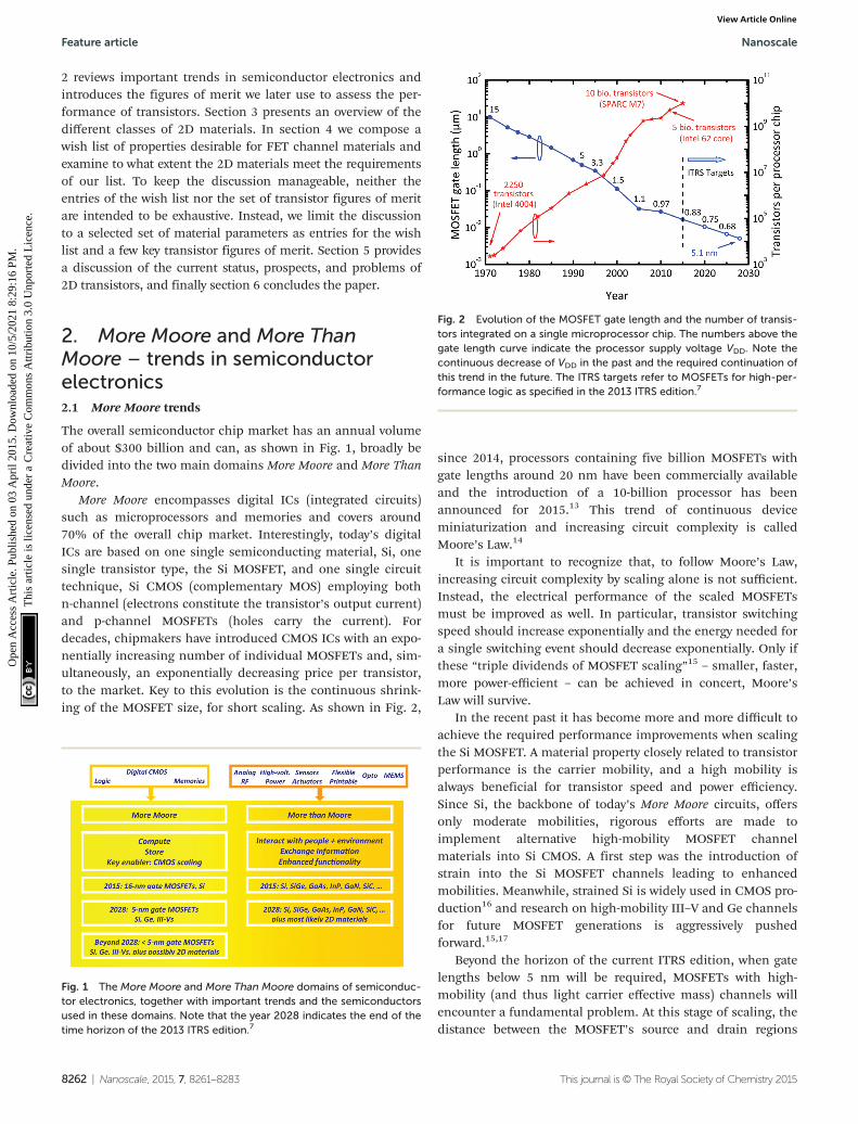
The overall semiconductor chip market has an annual volumeof about $300 billion and can, as shown in Fig. 1, broadly bedivided into the two main domains More Moore and More ThanMoore.
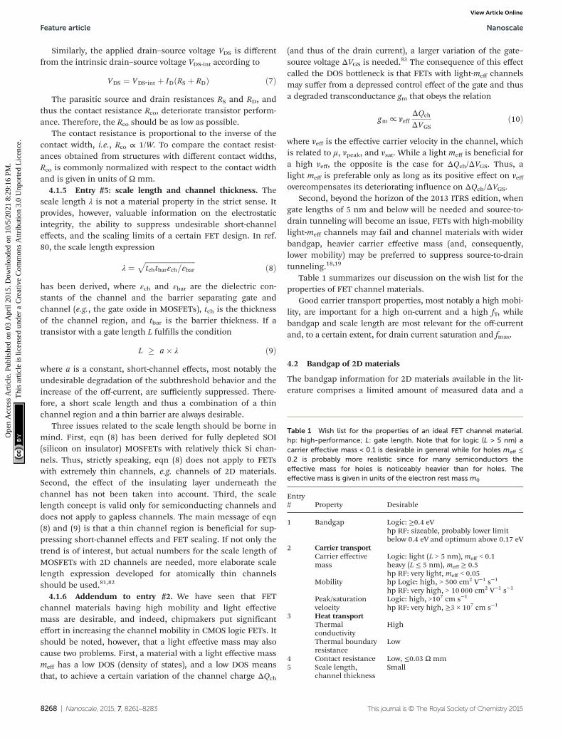
More Moore encompasses digital ICs (integrated circuits)such as microprocessors and memories and covers around70% of the overall chip market. Interestingly, today’s digitalICs are based on one single semiconducting material, Si, onesingle transistor type, the Si MOSFET, and one single circuittechnique, Si CMOS (complementary MOS) employing bothn-channel (electrons constitute the transistor’s output current)and p-channel MOSFETs (holes carry the current). Fordecades, chipmakers have introduced CMOS ICs with an expo-nentially increasing number of individual MOSFETs and, sim-ultaneously, an exponentially decreasing price per transistor,to the market. Key to this evolution is the continuous shrink-ing of the MOSFET size, for short scaling. As shown in Fig. 2,
since 2014, processors containing five billion MOSFETs withgate lengths around 20 nm have been commercially availableand the introduction of a 10-billion processor has beenannounced for 2015.13 This trend of continuous deviceminiaturization and increasing circuit complexity is calledMoore’s Law.14
It is important to recognize that, to follow Moore’s Law,increasing circuit complexity by scaling alone is not sufficient.Instead, the electrical performance of the scaled MOSFETsmust be improved as well. In particular, transistor switchingspeed should increase exponentially and the energy needed fora single switching event should decrease exponentially. Only ifthese “triple dividends of MOSFET scaling”15 – smaller, faster,more power-efficient – can be achieved in concert, Moore’sLaw will survive.
In the recent past it has become more and more difficult toachieve the required performance improvements when scalingthe Si MOSFET. A material property closely related to transistorperformance is the carrier mobility, and a high mobility isalways beneficial for transistor speed and power efficiency.Since Si, the backbone of today’s More Moore circuits, offersonly moderate mobilities, rigorous efforts are made toimplement alternative high-mobility MOSFET channelmaterials into Si CMOS. A first step was the introduction ofstrain into the Si MOSFET channels leading to enhancedmobilities. Meanwhile, strained Si is widely used in CMOS pro-duction16 and research on high-mobility III–V and Ge channelsfor future MOSFET generations is aggressively pushedforward.15,17
Beyond the horizon of the current ITRS edition, when gatelengths below 5 nm will be required, MOSFETs with high-mobility (and thus light carrier effective mass) channels willencounter a fundamental problem. At this stage of scaling, thedistance between the MOSFET’s source and drain regions
Fig. 1 The More Moore and More Than Moore domains of semiconduc-tor electronics, together with important trends and the semiconductorsused in these domains. Note that the year 2028 indicates the end of thetime horizon of the 2013 ITRS edition.7
Fig. 2 Evolution of the MOSFET gate length and the number of transis-tors integrated on a single microprocessor chip. The numbers above thegate length curve indicate the processor supply voltage VDD. Note thecontinuous decrease of VDD in the past and the required continuation ofthis trend in the future. The ITRS targets refer to MOSFETs for high-per-formance logic as specified in the 2013 ITRS edition.7
Feature article Nanoscale
8262 | Nanoscale, 2015, 7, 8261–8283 This journal is © The Royal Society of Chemistry 2015
Ope
n A
cces
s A
rtic
le. P
ublis
hed
on 0
3 A
pril
2015
. Dow
nloa
ded
on 1
0/5/
2021
8:2
9:16
PM
. T
his
artic
le is
lice
nsed
und
er a
Cre
ativ
e C
omm
ons
Attr
ibut
ion
3.0
Unp
orte
d L
icen
ce.
View Article Online

becomes so short that quantum-mechanical source–drain tun-neling impedes proper FET operation. It may turn out that forsub-5 nm MOSFETs heavy effective mass materials with lowermobilities will become preferable since a heavy carriereffective mass suppresses source–drain tunneling.18,19
2.2 More Than Moore trends
More Than Moore is not primarily focused on increasing circuitcomplexity but rather on enhancing the functionality of ICsand electronic systems by combining digital electronics withcomponents such as analog/RF (radio frequency) and high-voltage circuitry, sensors, actuators, etc. In the More ThanMoore domain, traditionally the material basis has been muchbroader compared to More Moore and, apart from Si, a varietyof alternative semiconductors is used to complement Si.
More Than Moore covers a wide and heterogeneous field,see Fig. 1. Here we focus solely on RF electronics where atpresent, in addition to Si, the compound semiconductorsbased on GaAs, InP, and GaN are very popular. It should benoted that in RF electronics only n-channel FETs are usedsince in most materials electrons are faster than holes. Amajor trend in RF electronics is the striving for higher transis-tor operating frequencies and for extending transistor oper-ation into the THz range. The evolution of the frequencyperformance of RF FETs in terms of the characteristic frequen-cies fT (cutoff frequency) and fmax (maximum frequency ofoscillation) is shown in Fig. 3.
As can be seen, the current record fmax of RF FETs is slightlyabove 1 THz, which means that FETs capable of THz amplifica-tion with reasonable power gain are still missing. On the otherhand, the frequency range around and above 1 THz is attrac-tive for applications in a variety of fields, such as security,medicine, and ultra-high-speed communications, to name justa few.40,41 Therefore, RF device engineers are looking foralternative FET channel materials offering improved mobilityand closely follow the research on 2D materials.
2.3 Transistor figures of merit
A FET consists of a channel region connecting two reservoirsof mobile charges called source and drain. The third electrode(gate) is separated from the channel by a thin barrier. Theapplied gate–source voltage VGS controls the conductivity ofthe channel and the applied drain–source voltage VDS drives adrain current ID through the transistor. Fig. 4 shows a genericFET, together with the structures of Si MOSFETs, III–V HEMTs,and 2D MOSFETs. FETs are devices with the ability (i) toswitch and (ii) to amplify signals and provide gain. For digitalelectronics, i.e., More Moore, switching is relevant while ampli-fying signals is important for RF applications.
In digital logic, the FET is supposed to switch between onand off. In the on-state, see Fig. 4(a), the channel has a lowresistance and a large on-current Ion can flow through it. Asper definition, Ion is the transistor current for the bias con-dition VGS = VDS = VDD. In the off-state, see Fig. 4(b), on theother hand, the FET should block the current, the channelresistance should be high, and only a very small off-current Ioffis allowed to flow. The off-current is defined as the currentflowing under the condition VGS = 0 and VDS = VDD. The gatevoltage at which the transistor is just at the verge of switchingon is the threshold voltage VTh. The transfer characteristics ofa MOSFET shown in Fig. 5 indicate that in the subthresholdregion (VGS < VTh) the drain current depends exponentially onVGS, followed by a transition region around VTh and finally bythe superthreshold region where the drain current is essen-tially linearly dependent on VGS. As we have shown in Fig. 2,the supply voltage VDD of logic circuits has been decreasedcontinuously over the years and a further reduction is requiredfor the future. This means that logic transistors must switchfrom off to on within a very limited range of VGS.
A further FOM (figure of merit) related to switching is theon–off ratio Ion/Ioff. For FETs to be used in digital logic, on–offratios in the range of ≈104–5 × 10⁷ are required.7 As a basicrule, Ioff should be as low as possible and both Ion and the on–off ratio should be as high as possible. A low Ioff is needed fora low static power consumption of logic circuits while a highIon is relevant for a high transistor switching speed.
When operated as an amplifier, on the other hand, the FETdoes not necessarily need to switch off. Instead, in most RFamplifier configurations the FET is permanently operated inthe on-state and small signals applied to its input, i.e., thegate, appear amplified at the output. The extent to which theinput signal is amplified is called gain. The small-signalcurrent gain, for example, is defined as the RF output currentof the transistor divided by the RF input current. Gains are fre-quency dependent and decrease with increasing frequency.Two important FOMs of RF transistors are the characteristicfrequencies fT and fmax. The cutoff frequency fT is the fre-quency at which the small-signal current gain h21 of the tran-sistor has dropped to unity (i.e., 0 dB) and the maximumfrequency of oscillation fmax is the frequency where the uni-lateral power gain U becomes unity. It should be noted that formost RF applications, power gain and fmax are more important
Fig. 3 Evolution of the cutoff frequency fT and maximum frequency ofoscillation fmax of RF FETs. Shown are the record fT and fmax valuesreported at a certain time. MESFET: metal-semiconductor FET; HEMT:high electron mobility transistor; pHEMT: pseudomorphic HEMT;mHEMT: metamorphic HEMT. Data are taken from ref. 20–39.
Nanoscale Feature article
This journal is © The Royal Society of Chemistry 2015 Nanoscale, 2015, 7, 8261–8283 | 8263
Ope
n A
cces
s A
rtic
le. P
ublis
hed
on 0
3 A
pril
2015
. Dow
nloa
ded
on 1
0/5/
2021
8:2
9:16
PM
. T
his
artic
le is
lice
nsed
und
er a
Cre
ativ
e C
omm
ons
Attr
ibut
ion
3.0
Unp
orte
d L
icen
ce.
View Article Online

than current gain and fT. Moreover, as a rule of thumb, theoperating frequency should be lower than 20% of the usedtransistors’ fmax to guarantee sufficient power gain. Fig. 6shows the small-signal current and power gains of an RF FETas a function of frequency, together with fT and fmax.
Commonly the voltage gain of RF FETs is not discussedexplicitly since, if both current and power gain are reported,this data pair contains information on the voltage gain.Because FETs with gapless channels, e.g. graphene MOSFETs,suffer from poor power gain, an inspection of the voltage gainis advisable, however. The frequency-dependent voltage gainAV is defined as
AV ¼ z21=z11 ð1Þ
where z21 and z11 are ac impedance parameters. At low fre-quencies, AV approaches the so-called intrinsic gain Gint
given as
Gint ¼ gm=gd ð2Þ
where gm is the transconductance (i.e., the slope of the transfercharacteristics, see Fig. 5, at the dc operating point) and gd isthe drain conductance (i.e., the slope of the ID–VDS outputcharacteristics). A transistor with low intrinsic gain, e.g.,caused by a large drain conductance, will always suffer from alow power gain.
All semiconductor devices generate fluctuations of voltageand current called noise. Noise is always undesirable andparticularly critical for the amplification of small RF signals.
Fig. 4 Basic FET structures. Generic structure of a FET (a) in the on-state and (b) in the off-state. (c) Conventional Si n-channel MOSFET. (d) HEMT.(e) 2D MOSFET. (f ) Back-gate 2D MOSFET frequently used for proof-of-concept purposes. Note that HEMTs and 2D MOSFETs do not possess pnjunctions as present in conventional Si MOSFETs shown in (c) but rather resemble the junctionless MOSFET which is intensively investigated atpresent.42
Fig. 5 Transfer characteristics of an n-channel FET showing the draincurrent ID as a function of the gate-source voltage VGS together with theon and off operating points for CMOS logic. Note that the scale of theleft current axis is logarithmic and that of the right current axis is linear.
Fig. 6 Small-signal current gain h21 and unilateral power gain U of a RFFET as a function of frequency, after ref. 43 and 44. The characteristicfrequencies fT and fmax are obtained by extrapolating the measured h21
and U with the characteristic slope of −20 dB per dec.
Feature article Nanoscale
8264 | Nanoscale, 2015, 7, 8261–8283 This journal is © The Royal Society of Chemistry 2015
Ope
n A
cces
s A
rtic
le. P
ublis
hed
on 0
3 A
pril
2015
. Dow
nloa
ded
on 1
0/5/
2021
8:2
9:16
PM
. T
his
artic
le is
lice
nsed
und
er a
Cre
ativ
e C
omm
ons
Attr
ibut
ion
3.0
Unp
orte
d L
icen
ce.
View Article Online

A measure for the noise generated in a transistor is the noisefigure NF, usually given in units of dB and defined as
NF dB½ � ¼ 10� logPSi=PNi
PSo=PNoð3Þ
where PSi and PSo are the signal powers at the input andoutput, and PNi and PNo are the noise powers at the input andoutput, respectively. Under optimum matching and bias con-ditions, the noise figure reaches a minimum called minimumnoise figure NFmin. It is the relevant FOM to characterize thenoise performance of RF transistors. For a good RF FET thecharacteristic frequencies fT and fmax should be high and theminimum noise figure NFmin should be low.
3. Overview of 2D materials
Inspired by the successful preparation of graphene, research-ers have intensively examined options to obtain stable 2Dmaterials beyond graphene. These efforts include real-worldexperiments where 2D materials have been prepared and ana-lyzed, as well as computational experiments where the thermo-dynamic stability and the band structure of existing andhypothetical 2D materials have been computed. For the latter,particularly the Atlas of 2D Materials reporting the propertiesof more than 140 different 2D materials45 is worthmentioning.
Recent experimental and theoretical efforts have shownthat a variety of 2D materials beyond graphene does or shouldexist and that their electronic properties span the full rangefrom metallic to insulating. Of particular interest for FETchannels are the semiconducting and, to a lesser extent, thegapless semi-metallic 2D materials. Fig. 7 shows schematicallythe relevant parts of the band structure of different classes ofthese 2D materials.
3.1 X-enes
Single-layer materials consisting of atoms of one singleelement arranged in a hexagonal lattice are designated asX-enes. So far, graphene as well as its Si-, Ge-, and P-based
counterparts silicene,46 germanene,47 and phosphorene48 havebeen experimentally realized, and the band structure ofstanene, the X-ene based on tin (Sn), has been calculated.49
Compared to graphene, much less is known on the otherX-enes. As of the end of 2014, the Web of Science databaselisted almost 91 000 entries under the search term graphenecompared to 654 entries for silicene, 133 for germanene, 81for phosphorene, and 8 for stanene.50 As shown in Fig. 7, gra-phene, silicene, germanene, and stanene are gapless and havecone-shaped conduction and valence bands. The cones are fre-quently called Dirac cones and, correspondingly, graphene,silicene, germanene, and stanene are designated as Diracmaterials. Phosphorene, on the other hand, is a semiconduc-tor with a sizeable gap.
3.2 X-anes
The crystallographic structure of the X-anes is closely relatedto that of the X-enes. They also possess a hexagonal lattice ofcarbon (graphane), silicon (silicane), germanium (germanane),or tin (stanane) atoms. However, their lattice atoms areadditionally out of plane bonded to hydrogen atoms – this isfrequently called hydrogenated. Graphane was predicted toexist in 200751 and was produced experimentally shortly after-wards.52 Recently, germanane could also be realized experi-mentally.53 Most relevant for electronic applications is the factthat graphane, silicane, and germanane possess sizeablebandgaps.
3.3 Fluoro-X-enes
The structure of these materials is very similar to that of theX-anes. Here, the lattice atoms are bonded out of plane to F(fluorine) atoms. Fluorographene has already been producedexperimentally and shown to have a wide gap of around, poss-ibly even exceeding, 3 eV.54,55 Theory has confirmed theseresults for fluorographene and predicted a gap around 1 eV forfluorosilicene while fluorogermanene seems to be gapless.45
3.4 TMDs
The TMDs constitute a group of materials consisting of a tran-sition metal M (elements of groups 4, 5, and 6 of the periodictable of elements) and a chalcogen Q, i.e., sulfur (S), selenium(Se), or tellurium (Te). These M and Q elements form co-valently bonded 2D layers of the MQ2 type (e.g., MoS2) with ahexagonal lattice. Single-layer TMDs consist of three atomiclayers where a layer of M atoms is sandwiched between twolayers of Q atoms. For example, single-layer MoS2 is composedof one layer of molybdenum atoms and two layers of sulfuratoms. Today, more than 40 different types of TMDs areknown.10 While many of them are metallic, those containingMo and W (i.e., MoS2, WSe2, etc.) as well as several of the Hf-,Pd-, Pt-, and Zr-based TMDs are semiconductors with band-gaps of the order of 1–2 eV.10,45 It should be noted that TMDsoccur in different polytypes 1T, 1T’, 2H, and 3R, where Tmeans trigonal, T’ distorted trigonal, H hexagonal, and Rrhombohedral, and 1, 2, or 3 indicates the number of TMDlayers in the unit cell,56,57 which have different properties. For
Fig. 7 Schematic band structure of 2D materials relevant for transistors.BLG: bilayer graphene; GNR: graphene nanoribbon; TMD: transitionmetal dichalcogenide; SMC: semimetal chalcogenide.
Nanoscale Feature article
This journal is © The Royal Society of Chemistry 2015 Nanoscale, 2015, 7, 8261–8283 | 8265
Ope
n A
cces
s A
rtic
le. P
ublis
hed
on 0
3 A
pril
2015
. Dow
nloa
ded
on 1
0/5/
2021
8:2
9:16
PM
. T
his
artic
le is
lice
nsed
und
er a
Cre
ativ
e C
omm
ons
Attr
ibut
ion
3.0
Unp
orte
d L
icen
ce.
View Article Online

example, the common 2H polytypes of the Mo- and W-basedTMDs are semiconducting while their metastable counterpartsof the 1T type are metallic.58
3.5 SMCs
SMCs consist of a semimetal M (Ga or In) and a chalcogen(S or Se). In contrast to the TMDs, they are expected to occur inM2X2 stoichiometry in a four-layer X–M–M–X configurationand to be semiconducting.45
3.6 MX-enes
There is a material class called the MAX phase family compris-ing more than 60 individual ternary layered materials.59 Thesematerials have a hexagonal lattice and the compositionMn+1AXn where M is an early transition metal, A is a group 13or 14 element, X is either carbon or nitrogen, and n is aninteger equal to 1, 2, or 3. The bonds between the M and Xatoms are much stronger than the M–A bonds so that the Aatoms can easily be removed, e.g., by an acid treatment. By asubsequent sonication, single Mn+1Xn layers, the so-called MX-enes, can be obtained. As the first MX-ene, Ti3C2 has been suc-cessfully prepared from the MAX material Ti3AlC2,
60 soon fol-lowed by the experimental verification of five further MX-enes,61 and the existence of even more MX-enes has been pre-dicted. Furthermore, F2, (OH)2, and O2 groups can be attachedto the pure MX-enes of the M2X configuration, resulting in theformation of the modified MX-enes M2XF2, M2X(OH)2, andMXO2.
62 Several modified MX-enes have been predicted to besemiconductors with sizeable bandgaps.62
3.7 Further 2D materials
By first-principles calculations, the phonon properties andband structures of entire classes of 2D IV–IV and III–V com-pounds and of many other 2D materials have been investi-gated. It has been shown that a large body of these 2Dmaterials with both hexagonal and tetragonal lattice structuresshould be stable and show bandgaps between 0.2 and5 eV.45,63,64 Although it is uncertain whether all these 2Dmaterials can be synthesized, at least part of them maybecome available for experiments in the future.
3.8 Production of 2D materials
To fabricate 2D transistors, first the 2D starting material mustbe produced, preferably in the form of large-area sheets withuniform thickness and high crystallographic quality. Layeredvan der Waals materials, where the stacked layers are boundby weak van der Waals forces, can be exfoliated. Mechanicalexfoliation is widely used to produce graphene,1 TMDs,6 andphosphorene48 layers. While this approach is simple and doesnot require expensive equipment, it is time consuming andprovides flakes of limited size only. Liquid exfoliation as asecond exfoliation method delivers 2D flakes dispersed in aliquid.65 This method is very effective, but the dispersed flakesare small, which makes transistor and circuit processingchallenging.
As an alternative, wafer-scale 2D materials can be grown onsubstrates. Epitaxial graphene on SiC has successfully beenformed and used for transistor processing.66 Graphene canalso be grown by CVD (chemical vapor deposition) on metalsand subsequently be transferred to insulating substrates suchas oxidized Si wafers.67 Furthermore, different TMDs such asMoS2, WS2, and WSe2 have been grown by CVD directly on oxi-dized Si wafers.68,69 Finally, silicene has been grown on metalsand transferred to SiO2/Si substrates for device processing.
70
4. Properties of 2D materials relevantfor transistors4.1 The ideal material for a FET channel – a wish list†
To assess the potential of novel materials for FET channels itis not sufficient to consider only one single material propertysuch as the carrier mobility. Instead, a set of properties shouldbe examined to get a realistic impression on the suitability ofthe new material for transistors. Therefore, in the following wecompose a (certainly not complete) wish list for the materialproperties of a FET channel, particularly for use in digital logicand RF FETs, and examine the extent to which the 2Dmaterials meet our wishes. In the discussion it should alwaysbe kept in mind that research on most of the 2D materials hasjust begun and is in an embryonic stage compared to the con-ventional 3D bulk semiconductors such as Si, Ge, and the III–V compounds. This leads to the situation that, while our wishlist itself is well established and relies on the experiences ofdecades of transistor research, the available data for the rele-vant properties of the 2D materials are rather fragmentary.
4.1.1 Wish list entry #1: bandgap. The bandgap is a keyproperty of semiconductors. It decisively affects their applica-bility to electronic devices and the existence of a gap is essen-tial for proper FET operation. As discussed in section 2.3, FETsfor digital logic need a high on–off ratio. While the on-currentof a FET is not directly related to the bandgap EG, the off-current strongly depends on EG according to
Ioff / exp�EG
mkBTð4Þ
where m is a factor of 2 (ref. 72) or larger (depending on thespecific FET design), kB is the Boltzmann constant, and T isthe temperature. Thus, the on–off ratio follows
IonIoff
/ expEG
mkBTð5Þ
Estimations suggest that at room temperature a gap of theorder of 400 meV is needed to achieve a sufficiently goodswitch-off and the required on–off ratios.72–74
Since RF FETs can permanently be operated in the on-stateand do not need to switch off, one might conclude that here agap is not needed. Unfortunately, the situation is more
†The idea for the title of this section originates from ref. 71.
Feature article Nanoscale
8266 | Nanoscale, 2015, 7, 8261–8283 This journal is © The Royal Society of Chemistry 2015
Ope
n A
cces
s A
rtic
le. P
ublis
hed
on 0
3 A
pril
2015
. Dow
nloa
ded
on 1
0/5/
2021
8:2
9:16
PM
. T
his
artic
le is
lice
nsed
und
er a
Cre
ativ
e C
omm
ons
Attr
ibut
ion
3.0
Unp
orte
d L
icen
ce.
View Article Online

complex. It has been discussed in detail that to achieve a highpower gain and high fmax, the FET needs to show a sufficientlygood saturation of the drain current and for that, in turn, agap is needed.3 Current gain and fT, on the other hand, areless affected by a missing or weak current saturation. Thus,transistors with gapless channels can provide high currentgain and fT but suffer from poor power gain and fmax. It is notexactly known how wide the gap of the channel of a good RFFET should be. Most likely, the requirements are less stringentthan for logic FETs. The fastest and least noisy RF FETs areInP HEMTs32 and GaAs mHEMTs75,76 having InxGa1−xAs chan-nels with high In contents x ranging from 0.7 (EG ≈ 0.65 eV) to1 (i.e., InAs, EG = 0.35 eV). Experiments with InSb channelHEMTs (EG InSb = 0.17 eV), on the other hand, revealed thatthese transistors, despite being fast, show lower fT and fmax com-pared to InP HEMTs and GaAs mHEMTs with a similar gatelength.77,78 This suggests that the 0.17 eV gap of InSb mightalready be too narrow for ultra-high-performance RF FETs.
4.1.2 Entry #2: carrier transport and effective mass. Logicand RF FETs should be fast, i.e., they should react quickly onvariations of their input signals, and show a large on-statecurrent. For this, fast carriers are needed. Measures for thespeed of carrier transport are the mobility µ, the peak velocityvpeak, and the saturation velocity vsat. When a low electric fieldE acts on a carrier, its drift velocity v is given by v = µ × E. Themobility is inversely proportional to the carrier effective massmeff and a light meff is a precondition for a high µ. Under high-field conditions, the carrier velocity no longer follows the fieldlinearly. The high-field velocity for holes shows a soft satur-ation and approaches vsat at high fields. For electrons, the situ-ation is more diverse. In some semiconductors (e.g., GaAs), theelectron velocity shows a pronounced peak (vpeak) at a certainfield, then decreases at higher fields, and eventuallyapproaches the saturation velocity. In other semiconductors,e.g., Si, soft saturation without a velocity peak occurs. Fig. 8shows exemplarily the v–E (velocity–electric field) character-istics for electrons and holes in Si and GaAs. The channelmaterial of a fast FET should show a high mobility (and thus alight meff ), preferably combined with a high vpeak and/or vsat.
For logic FETs, a high mobility and a high saturation velo-city are always desirable. It should be mentioned, however,that Si MOSFETs show surprisingly good switching character-istics in spite of the rather moderate µ (200–500 cm2 V−1 s−1)and vsat (10
7 cm s−1). The InxGa1−xAs channels of the best RFFETs, i.e., InP HEMTs and GaAs mHEMTs, show mobilities of10 000–15 000 cm2 V−1 s−1 and peak velocities of 3–4 × 10⁷ cms−1, and alternative channel materials that are to compete withInxGa1−xAs for high-performance RF FETs should show at leastsimilar transport characteristics, combined with an appropri-ate bandgap. Reasonably good RF performance, however, canbe achieved already with lower mobility channels, e.g., Si chan-nels of RF Si MOSFETs, provided the contact resistance (seeentry #4) is low and the scale length (entry #5) is short.
4.1.3 Entry #3: heat transport. If a voltage is applied to aFET and a current is flowing through its channel, electricalenergy is converted into heat and this heat must be removedto avoid unacceptable self-heating. To accomplish an effectiveheat removal, the channel material should show a highthermal conductivity κ.
The thermal conductivity of the channel material, however,does not tell the whole story of heat transport, in particular ifthe transistor is located on a substrate different from thechannel material. 2D FETs, such as graphene or TMD FETs(see Fig. 4e showing a MoS2 MOSFET), are frequentlyrealized on the surface of oxidized Si wafers. Here, the heatgenerated in the channel first has to cross the channel–SiO2
interface acting as a thermal boundary resistance RTB, movethrough the SiO2 layer, and then cross the SiO2–substrate inter-face forming a second RTB before it can spread across the Sisubstrate.79 To limit self-heating, the thermal conductivity ofthe FET channel material and of all materials underneathshould be high and the thermal boundary resistances of allinterfaces between the channel and the back side of the chipshould be low.
4.1.4 Entry #4: contact resistance. In a FET, the gate–source voltage controls the channel conductivity and thus thedrain current ID. A closer inspection shows that not the gate–source voltage applied between the gate and source terminals,but rather the intrinsic gate–source voltage VGS-int, i.e., thepotential difference between the gate and the source-sidedend of the channel, is controlling the current. Carrierscoming from the source terminal first cross the metal–semi-conductor interface which hinders the carrier flow and acts asa resistance called source contact resistance Rco-S. Next, thecarriers flow through an ungated semiconductor regionuntil they reach the channel underneath the gate.This ungated region represents the source series resistanceRser-S. The overall parasitic resistance at the source side, RS,is the sum Rco-S + Rser-S. The same situation occurs at thedrain side of the FET leading to the parasitic drainresistance RD.
Due to the voltage drop across RS, part of the applied VGS islost for the control of the current as can be seen from
VGS ¼ VGS-int þ IDðRco-S þ Rser-SÞ ¼ VGS-int þ IDRS ð6ÞFig. 8 Velocity-field characteristics for electrons and holes in Si andGaAs. Note the peak of the electron velocity in GaAs and the soft satur-ation of the other v–E characteristics.
Nanoscale Feature article
This journal is © The Royal Society of Chemistry 2015 Nanoscale, 2015, 7, 8261–8283 | 8267
Ope
n A
cces
s A
rtic
le. P
ublis
hed
on 0
3 A
pril
2015
. Dow
nloa
ded
on 1
0/5/
2021
8:2
9:16
PM
. T
his
artic
le is
lice
nsed
und
er a
Cre
ativ
e C
omm
ons
Attr
ibut
ion
3.0
Unp
orte
d L
icen
ce.
View Article Online
Similarly, the applied drain–source voltage VDS is differentfrom the intrinsic drain–source voltage VDS-int according to
VDS ¼ VDS-int þ IDðRS þ RDÞ ð7ÞThe parasitic source and drain resistances RS and RD, and
thus the contact resistance Rco, deteriorate transistor perform-ance. Therefore, the Rco should be as low as possible.
The contact resistance is proportional to the inverse of thecontact width, i.e., Rco ∝ 1/W. To compare the contact resist-ances obtained from structures with different contact widths,Rco is commonly normalized with respect to the contact widthand is given in units of Ω mm.
4.1.5 Entry #5: scale length and channel thickness. Thescale length λ is not a material property in the strict sense. Itprovides, however, valuable information on the electrostaticintegrity, the ability to suppress undesirable short-channeleffects, and the scaling limits of a certain FET design. In ref.80, the scale length expression
λ ¼ffiffiffiffiffiffiffiffiffiffiffiffiffiffiffiffiffiffiffiffiffiffiffiffiffiffiffiffitchtbarεch=εbar
pð8Þ
has been derived, where εch and εbar are the dielectric con-stants of the channel and the barrier separating gate andchannel (e.g., the gate oxide in MOSFETs), tch is the thicknessof the channel region, and tbar is the barrier thickness. If atransistor with a gate length L fulfills the condition
L � a� λ ð9Þwhere a is a constant, short-channel effects, most notably theundesirable degradation of the subthreshold behavior and theincrease of the off-current, are sufficiently suppressed. There-fore, a short scale length and thus a combination of a thinchannel region and a thin barrier are always desirable.
Three issues related to the scale length should be borne inmind. First, eqn (8) has been derived for fully depleted SOI(silicon on insulator) MOSFETs with relatively thick Si chan-nels. Thus, strictly speaking, eqn (8) does not apply to FETswith extremely thin channels, e.g. channels of 2D materials.Second, the effect of the insulating layer underneath thechannel has not been taken into account. Third, the scalelength concept is valid only for semiconducting channels anddoes not apply to gapless channels. The main message of eqn(8) and (9) is that a thin channel region is beneficial for sup-pressing short-channel effects and FET scaling. If not only thetrend is of interest, but actual numbers for the scale length ofMOSFETs with 2D channels are needed, more elaborate scalelength expression developed for atomically thin channelsshould be used.81,82
4.1.6 Addendum to entry #2. We have seen that FETchannel materials having high mobility and light effectivemass are desirable, and indeed, chipmakers put significanteffort in increasing the channel mobility in CMOS logic FETs. Itshould be noted, however, that a light effective mass may alsocause two problems. First, a material with a light effective massmeff has a low DOS (density of states), and a low DOS meansthat, to achieve a certain variation of the channel charge ΔQch
(and thus of the drain current), a larger variation of the gate–source voltage ΔVGS is needed.83 The consequence of this effectcalled the DOS bottleneck is that FETs with light-meff channelsmay suffer from a depressed control effect of the gate and thusa degraded transconductance gm that obeys the relation
gm / veffΔQch
ΔVGSð10Þ
where veff is the effective carrier velocity in the channel, whichis related to µ, vpeak, and vsat. While a light meff is beneficial fora high veff, the opposite is the case for ΔQch/ΔVGS. Thus, alight meff is preferable only as long as its positive effect on veffovercompensates its deteriorating influence on ΔQch/ΔVGS.
Second, beyond the horizon of the 2013 ITRS edition, whengate lengths of 5 nm and below will be needed and source-to-drain tunneling will become an issue, FETs with high-mobilitylight-meff channels may fail and channel materials with widerbandgap, heavier carrier effective mass (and, consequently,lower mobility) may be preferred to suppress source-to-draintunneling.18,19
Table 1 summarizes our discussion on the wish list for theproperties of FET channel materials.
Good carrier transport properties, most notably a high mobi-lity, are important for a high on-current and a high fT, whilebandgap and scale length are most relevant for the off-currentand, to a certain extent, for drain current saturation and fmax.
4.2 Bandgap of 2D materials
The bandgap information for 2D materials available in the lit-erature comprises a limited amount of measured data and a
Table 1 Wish list for the properties of an ideal FET channel material.hp: high-performance; L: gate length. Note that for logic (L > 5 nm) acarrier effective mass < 0.1 is desirable in general while for holes meff ≤0.2 is probably more realistic since for many semiconductors theeffective mass for holes is noticeably heavier than for holes. Theeffective mass is given in units of the electron rest mass m0
Entry# Property Desirable
1 Bandgap Logic: ≥0.4 eVhp RF: sizeable, probably lower limitbelow 0.4 eV and optimum above 0.17 eV
2 Carrier transportCarrier effectivemass
Logic: light (L > 5 nm), meff < 0.1heavy (L ≤ 5 nm), meff ≥ 0.5hp RF: very light, meff < 0.05
Mobility hp Logic: high, > 500 cm2 V−1 s−1
hp RF: very high, > 10 000 cm2 V−1 s−1
Peak/saturationvelocity
Logic: high, >107 cm s−1
hp RF: very high, ≥3 × 107 cm s−1
3 Heat transportThermalconductivity
High
Thermal boundaryresistance
Low
4 Contact resistance Low, ≤0.03 Ω mm5 Scale length,
channel thicknessSmall
Feature article Nanoscale
8268 | Nanoscale, 2015, 7, 8261–8283 This journal is © The Royal Society of Chemistry 2015
Ope
n A
cces
s A
rtic
le. P
ublis
hed
on 0
3 A
pril
2015
. Dow
nloa
ded
on 1
0/5/
2021
8:2
9:16
PM
. T
his
artic
le is
lice
nsed
und
er a
Cre
ativ
e C
omm
ons
Attr
ibut
ion
3.0
Unp
orte
d L
icen
ce.
View Article Online

wide body of results obtained from first-principle (ab initio)calculations. Calculations provide not only the bandgap itself,but the entire band structure, from which the carrier effectivemasses can be extracted. Thus, first-principle calculations area very useful means of assessing the suitability of a semi-conductor for FET channels. It should be mentioned, however,that different methods of first-principle calculations can leadto quite different bandgaps for one and the same material.The popular DFT (density functional theory) systematicallyunderestimates the bandgap, while computationally moredemanding approaches, such as GW, predict wider gapswhich, however, in some cases exceed the measured gaps.45,84
Two examples for the considerable differences between thebandgaps obtained from DFT calculations and those calcu-lated using more rigorous methods are given below. For ger-manane, the bandgap predicted by DFT ranges from 0.95 eV85
to 1.53 eV53 compared to values in the range of 1.84 eV45 to3.6 eV86 obtained by other methods and a measured gap of1.59 eV.53 As a second example we consider GNRs. For N =7 armchair GNRs (N is the number of carbon atoms along theGNR width and N = 7 corresponds to a width of about0.74 nm), a gap of 3.8 eV has been calculated by the GWmethod87 compared to 1.5–1.6 eV obtained by DFT87,88 andmeasured gaps of 2.3–2.8 eV.89,90 Thus, calculated bandgapsshould be treated as estimates rather than accurate predic-tions, and those obtained by DFT calculations as a lower limit.On the other hand, the shape of the individual bands calcu-lated by DFT and the extracted carrier effective masses can beconsidered as reasonable guides.45
Large-area graphene is gapless and the same holds for sili-cene and germanene.45 There are, however, options to open agap in these materials. For graphene, the first approach is toform narrow GNRs by either chemical synthesis91,92 or litho-graphic patterning.93,94 Chemically synthesized GNRs withatomically precise edges have been reported while patternedGNRs typically show non-ideal edges that degrade carriertransport. Fig. 9 compiles theoretical bandgap data (calculatedby the GW method) together with experimental bandgap datafor GNRs and shows the general trend of an increasing gap fordecreasing width. As can be seen, narrow ribbons having awidth of 10 nm or less are needed to achieve the 0.4 eV gaprequired for digital logic.
The second option to open a gap in graphene is by applyinga perpendicular electric field to BLG, i.e., two graphene layers,one located directly on top of the other.96,97 As shown inFig. 7, the conduction and valence bands of biased BLG arenot parabolic as for most other semiconductors, but Mexican-hat-shaped.96 For FET-relevant BLG structures, realisticallygaps up to 130 meV can be expected.97 This might be helpfulfor RF FETs but is not sufficient for digital logic FETs.
Recent calculations have predicted a gap opening in sili-cene and germanene nanoribbons98 as well as in single-layersilicene and germanene when a vertical electric field isapplied.99 For a given field, however, the gap in silicene andgermanene is smaller than that in biased BLG. Thus, regard-ing the bandgap, large-area silicene and germanene are not
suited for logic FETs and their potential for RF FETs isunclear.
The bandgaps of the 2D materials (except Dirac materials,nanoribbons, BLG, and biased silicene and germanene) aresummarized in Fig. 10. To guarantee consistency, all gapsshown are calculated by DFT. True semiconductors (EG = 0.5–2eV) are phosphorene, germanane, fluorosilicene, the Mo- and
Fig. 9 Bandgap of GNRs vs. ribbon width. Shown are theoretical dataobtained by the GW method for ac (armchair) GNRs of the 3p, 3p + 1,and 3p + 2 families (full triangles and lines, p is an integer) and for zz(zigzag) GNRs from ref. 87, together with measured results for chemi-cally synthesized89,90,95 and lithographically patterned93,94 GNRs.
Fig. 10 Bandgap of semiconducting and insulating 2D materials calcu-lated by DFT (data taken from ref. 45 unless otherwise stated). Theletters indicate the material class. (a) Semiconducting X-enes (phos-phorene,100 note that graphene, silicene, and germanene are gapless).(b) X-anes (from top to bottom graphane, silicane, germanane). (c)Fluoro-X-enes (fluorographene, fluorosilicene, note that fluorogerma-nene is gapless). (d) Mo-based TMDs (MoS2, MoSe2, MoTe2). (e) W-basedTMDs (WS2, WSe2, WTe2). (f ) Further disulfides (HfS2, ZrS2, TiS2). (g)SMCs (GaS, InS, GaSe, InSe). (h) MX-enes62,101 (top: Sc2CO2, middle:Hf2CO2, Sc2CF2, Ti2CO2 (all 1 eV), bottom: Zr2CO2). (i) BN, SiC. Alsoshown are the gaps of conventional 3D semiconductors labeled asmaterial class k (GaN, GaAs, Si, In0.53Ga0.47As, Ge, InAs).
Nanoscale Feature article
This journal is © The Royal Society of Chemistry 2015 Nanoscale, 2015, 7, 8261–8283 | 8269
Ope
n A
cces
s A
rtic
le. P
ublis
hed
on 0
3 A
pril
2015
. Dow
nloa
ded
on 1
0/5/
2021
8:2
9:16
PM
. T
his
artic
le is
lice
nsed
und
er a
Cre
ativ
e C
omm
ons
Attr
ibut
ion
3.0
Unp
orte
d L
icen
ce.
View Article Online

W-based TMDs, as well as HfS2, ZrS2, and TiS2, GaSe, InSe,and several MX-enes. Graphane, silicane, fluorographene, GaS,InS, and SiC can be considered as wide bandgap semiconduc-tors while BN is an insulator. For comparison, bandgap datafor conventional 3D semiconductors widely used for FET chan-nels are also shown in Fig. 10.
Due to its wide gap, BN is not really a candidate channelmaterial. It has, however, successfully been used as a gatedielectric for graphene MOSFETs102 and moreover shown tohave a beneficial effect on the mobility in graphene channelsunderneath or above it.102,103
The bandgap of TMDs and phosphorene depends on thelayer number. It is widest for single layers and graduallydecreases with increasing layer number toward the bulk value.This is important since the channels of experimental TMDand phosphorene MOSFETs frequently consist of few-layermaterial instead of single layers. The thickness dependence ofthe gap is particularly pronounced for phosphorene where thegap decreases from 1 eV for single layers (see Fig. 10) down to0.67 and 0.52 eV for bilayer and trilayer materials.100
In summary we state that in terms of bandgap many 2Dmaterials fulfill the requirements of our wish list and thereforeare suitable for FET channels.
4.3 Carrier transport and effective mass
It is well established that the carrier mobility of semiconduc-tors tends to decrease with increasing bandgap. From Fig. 11showing this trend for the electron mobility µn, we see that forthe III–V compounds (black full circles), the electron mobility
reduces from 77 000 cm2 V−1 s−1 for the narrow-bandgap InSbto 3000 cm2 V−1 s−1 for the wider-bandgap Ga0.51In0.49P (EG =1.85 eV). Si (EG = 1.12 eV) and Ge (EG = 0.66 eV) follow this ten-dency although for these materials the electron mobility is lowerthan that of the III–V compounds with a comparable gap. Alsographene cannot escape from this mobility-bandgap trend. Sus-pended gapless graphene shows very high electron mobilities ofup to 200 000 cm2 V−1 s−1. The electron mobility in gapless gra-phene on insulating substrates is lower, but still impressivelyhigh as shown in Table 2. The gap opening in GNRs and biasedBLG results, however, in a dramatic mobility reduction.
The electron mobility data reported by early 2015 for 2Dmaterials beyond graphene are also included in Fig. 11. ForMoS2, phonon limited mobilities, i.e., the upper mobility limitfor defect-free undoped material, ranging from 130 cm2 V−1
s−1 (ref. 104) to 410 cm2 V−1 s−1 (ref. 107), have been calculatedand mobilities between 1 and 300 cm2 V−1 s−1 have beenextracted from experimental MoS2 MOSFET structures, see,e.g., ref. 6, 109–112. Note that (i) the mobility reported forback-gated MoS2 MOSFETs (a few to a few tens of cm2 V−1 s−1)is lower than the mobility observed in top-gated MoS2 FETs(several tens to a few hundreds of cm2 V−1 s−1), and (ii) for top-gated MoS2 FETs occasionally electron mobilities of up to1000 cm2 V−1 s−1 (ref. 121) have been reported. These data arenot included in Fig. 11 since it most likely results from an ir-regular extraction approach.122,123
For single-layer WSe2, a hole mobility of 250 cm2 V−1 s−1
has been reported126 that compares favorably with the bestelectron mobilities around 200 cm2 V−1 s−1 observed in multi-layer WSe2
114 and in ref. 127 it has been shown that the holemobility in WSe2 can indeed be higher than the electron mobi-lity. In few-layer phosphorene, a remarkable hole mobility of1000 cm2 V−1 s−1 has been measured.128
Velocity-field characteristics for gapless graphene have beensimulated and measured, and for BLG, GNRs, silicene, andMoS2 high-field transport data have been simulated. Thereported v–E characteristics of 2D materials show a soft satur-ation with a slight decline of the velocity at high fields. Table 3summarizes the available saturation and peak velocity data for2D materials. These high-field transport data can be comparedwith the v–E characteristics for Si and GaAs in Fig. 8.
It should be mentioned that for future generations of Si-based logic ICs, ultra-thin-body SOI MOSFETs and possibly Sinanowire MOSFETs with ultra-small body cross-section will be
Fig. 11 Room-temperature electron mobility vs. bandgap for differentmaterials. The data for the conventional 3D bulk semiconductors takenfrom the compilation in ref. 44 relate to undoped material. III–Vmaterials (black solid circles), from left to right InSb, InAs, In0.53Ga0.47As,InP, GaAs, In0.52Al0.48As, Al0.3Ga0.7As, Ga0.51In0.49P. Experimental data forgraphene and simulated mobilities for GNRs and BLG taken from thecompilation in ref. 3. Calculated mobilities for silicene and germanenetaken from ref. 104–106. Simulated MoS2 mobilities taken from ref. 104,107 and 108, experimental MoS2 data taken exemplarily from ref. 6 and109–112, and those for WS2, MoSe2 and WSe2 from ref. 113, 114, 124 and125.
Table 2 Measured electron mobility in gapless graphene produced bydifferent methods. Note that the predicted upper limit for the mobility ingapless graphene on SiO2/Si is 40 000 cm2 V−1 s−1 (ref. 120)
Graphenetype
Supporting layer/substrate
Mobility(cm2 V−1 s−1) Ref.
Exfoliated SiO2/Si 24 000 115Exfoliated WS2/SiO2/Si 38 000 116CVD SiO2/Si 16 000 117Epitaxial Si-face SiC 2000 118Epitaxial C-face SiC 8700 119
Feature article Nanoscale
8270 | Nanoscale, 2015, 7, 8261–8283 This journal is © The Royal Society of Chemistry 2015
Ope
n A
cces
s A
rtic
le. P
ublis
hed
on 0
3 A
pril
2015
. Dow
nloa
ded
on 1
0/5/
2021
8:2
9:16
PM
. T
his
artic
le is
lice
nsed
und
er a
Cre
ativ
e C
omm
ons
Attr
ibut
ion
3.0
Unp
orte
d L
icen
ce.
View Article Online

needed and that in these structures, the mobility is degradedand much smaller compared to bulk Si. For example, in sub-5 nm diameter Si nanowire MOS structures, the electron mobi-lity at low perpendicular effective fields can be below 100 cm2
V−1 s−1 and drop further at higher effective fields down to afew tens of cm2 V−1 s−1.133,134 Thus, several 2D semiconductorscan be considered as a viable alternative.
If carrier transport data for a new material are not available,an examination of the material’s band structure and carriereffective mass can be helpful. Although the effective mass isnot the only quantity influencing the mobility, a light effectivemass is always an indication for a high mobility. In Fig. 12 theelectron effective mass of 2D materials and of conventionalsemiconductors is plotted as a function of the bandgap.
For conventional semiconductors (Si, Ge, III–V compounds)the hole mobility µp is always lower than the electron mobility.This is particularly true for the III–V compounds with veryhigh electron mobility. The ratio µp/µn is around 0.5 for Ge, 0.3
for Si, 0.05 for GaAs, and approaches 0.01 for the narrowbandgap compounds InAs and InSb. For the Mo- and W-basedTMDs45 and for germanane,53 as well as for phosphorene fortransport in the armchair direction,100,136,137 meff-n/meff-p ratios(meff-n and meff-p are the electron and hole effective masses) of0.8–1 have been calculated and band structure calculations forBLG and GNRs also reveal a high degree of symmetry of thetop of the valence band and the bottom of the conductionband. This suggests µp/µn ratios close to unity for thesematerials. For CMOS logic, µn ≈ µp is highly desirable sinceunder these conditions a symmetric design of n- andp-channel MOSFETs is possible.
When comparing the electron mobilities of the 2Dmaterials in Fig. 11 with those of the conventional 3D semi-conductors it seems that the semiconducting 2D materialsshow rather moderate mobilities and, with the exception ofgermanene, do not compete well. This leads us to the con-clusion that the 2D materials cannot compete with the high-mobility III–V compounds and will not be suitable for ultra-fast high-performance transistors. On the other hand, theirmobilities are appropriate for many other applications wherehigh speed is not of primary importance. The calculated elec-tron mobility of more than 18 000 cm2 V−1 s−1 for germa-nane,106 on the other hand, is very promising. However, thisresult needs to be confirmed by experiments and to be repro-duced by calculations of other groups.
4.4 Heat transport
Table 4 summarizes the currently available data for thethermal conductivity of 2D materials in comparison with thatof 3D bulk materials. The thermal conductivity of suspendedgraphene exceeds that of metals (e.g., κCu = 400 W m−1 K−1)and the maximum reported record value from ref. 138 is evenabove that of bulk graphite. The thermal conductivity of gra-phene on SiO2 is still high but lower compared to suspendedgraphene due to interface interactions. GNRs as well as theMo- and W-based TMDs show lower thermal conductivities.
Table 5 shows the thermal boundary resistance RTB of gra-phene/SiO2, graphene/SiC, and graphene/BN junctions and forcomparison that of silicon on SiO2 as used in modern SOIstructures. Unfortunately, information on the thermal bound-ary resistance for the 2D materials beyond graphene is not yet
Fig. 12 Electron effective mass of 2D and conventional 3D semi-conductors vs. bandgap. III–V compounds (black solid circles), from leftto right InSb, InAs, In0.53Ga0.47As, InP, GaAs, Al0.3Ga0.7As. Data for TMDsand graphane from ref. 45, for germanane from ref. 53, for GNRs fromref. 135, and for phosphorene from ref. 136 and 137. The numbers at theGNR data points indicate the ribbon width according to the width–gaprelationship from ref. 87.
Table 3 Peak and saturation velocities for 2D materials and the corresponding fields (in kV cm−1) and carrier sheet densities
Material vpeak (107 cm s−1) vsat (10
7 cm s−1) Comment Ref.
Graphene — 1–3 @ 20 Exp. + fit, different nS 129Graphene 5.8 @ 15 5.2 @ 50 Sim., nS = 1011 cm−2 130BLG 3.4 @ 5 2.9 @ 20 Sim., nS = 5 × 1011 cm−2 131BLG — 3.0 @ 25 Sim., nS = 1012 cm−2, EG = 0.1 eV 130GNR 3.7 @ 10 <3 @ >30 Sim., nS = 1012 cm−2, w = 10.1 nm 132
>3.1 @ >100 — Sim., nS = 1012 cm−2, w = 2.62 nmGNR — 3.3 @ 25 Sim., nS = 1012 cm−2, EG = 0.4 eV 130Silicene 0.5 @ 30 0.46 @ 50 Sim. 104
0.39 @ 100MoS2 — 0.34 @ 100 Sim. 104MoS2 — 1.5 @ 100 Sim. 108
Nanoscale Feature article
This journal is © The Royal Society of Chemistry 2015 Nanoscale, 2015, 7, 8261–8283 | 8271
Ope
n A
cces
s A
rtic
le. P
ublis
hed
on 0
3 A
pril
2015
. Dow
nloa
ded
on 1
0/5/
2021
8:2
9:16
PM
. T
his
artic
le is
lice
nsed
und
er a
Cre
ativ
e C
omm
ons
Attr
ibut
ion
3.0
Unp
orte
d L
icen
ce.
View Article Online
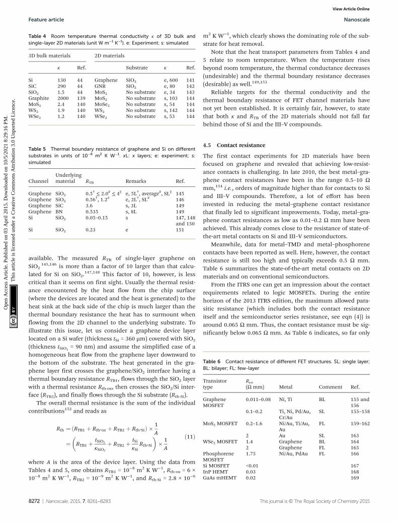
available. The measured RTB of single-layer graphene onSiO2
145,146 is more than a factor of 10 larger than that calcu-lated for Si on SiO2.
147,148 This factor of 10, however, is lesscritical than it seems on first sight. Usually the thermal resist-ance encountered by the heat flow from the chip surface(where the devices are located and the heat is generated) to theheat sink at the back side of the chip is much larger than thethermal boundary resistance the heat has to surmount whenflowing from the 2D channel to the underlying substrate. Toillustrate this issue, let us consider a graphene device layerlocated on a Si wafer (thickness tSi = 360 µm) covered with SiO2
(thickness tSiO2= 90 nm) and assume the simplified case of a
homogeneous heat flow from the graphene layer downward tothe bottom of the substrate. The heat generated in the gra-phene layer first crosses the graphene/SiO2 interface having athermal boundary resistance RTB1, flows through the SiO2 layerwith a thermal resistance Rth-ox, then crosses the SiO2/Si inter-face (RTB2), and finally flows through the Si substrate (Rth-Si).
The overall thermal resistance is the sum of the individualcontributions152 and reads as
Rth ¼ RTB1 þ Rth-ox þ RTB2 þ Rth-Sið Þ � 1A
¼ RTB1 þ tSiO2
κSiO2
þ RTB2 þ tSiκSi
Rth-Si
� �� 1A
ð11Þ
where A is the area of the device layer. Using the data fromTables 4 and 5, one obtains RTB1 = 10−8 m2 K W−1, Rth-ox = 6 ×10⁻⁸ m2 K W−1, RTB2 = 10−9 m2 K W−1, and Rth-Si = 2.8 × 10⁻⁶
m2 K W−1, which clearly shows the dominating role of the sub-strate for heat removal.
Note that the heat transport parameters from Tables 4 and5 relate to room temperature. When the temperature risesbeyond room temperature, the thermal conductance decreases(undesirable) and the thermal boundary resistance decreases(desirable) as well.149,153
Reliable targets for the thermal conductivity and thethermal boundary resistance of FET channel materials havenot yet been established. It is certainly fair, however, to statethat both κ and RTB of the 2D materials should not fall farbehind those of Si and the III–V compounds.
4.5 Contact resistance
The first contact experiments for 2D materials have beenfocused on graphene and revealed that achieving low-resist-ance contacts is challenging. In late 2010, the best metal–gra-phene contact resistances have been in the range 0.5–10 Ωmm,154 i.e., orders of magnitude higher than for contacts to Siand III–V compounds. Therefore, a lot of effort has beeninvested in reducing the metal–graphene contact resistancethat finally led to significant improvements. Today, metal–gra-phene contact resistances as low as 0.01–0.2 Ω mm have beenachieved. This already comes close to the resistance of state-of-the-art metal contacts on Si and III–V semiconductors.
Meanwhile, data for metal–TMD and metal–phosphorenecontacts have been reported as well. Here, however, the contactresistance is still too high and typically exceeds 0.5 Ω mm.Table 6 summarizes the state-of-the-art metal contacts on 2Dmaterials and on conventional semiconductors.
From the ITRS one can get an impression about the contactrequirements related to logic MOSFETs. During the entirehorizon of the 2013 ITRS edition, the maximum allowed para-sitic resistance (which includes both the contact resistanceitself and the semiconductor series resistance, see eqn (4)) isaround 0.065 Ω mm. Thus, the contact resistance must be sig-nificantly below 0.065 Ω mm. As Table 6 indicates, so far only
Table 5 Thermal boundary resistance of graphene and Si on differentsubstrates in units of 10−8 m2 K W−1. xL: x layers; e: experiment; s:simulated
ChannelUnderlyingmaterial RTB Remarks Ref.
Graphene SiO2 0.5† ≤ 2.0# ≤ 4§ e, 5L†, average#, SL§ 145Graphene SiO2 0.56†, 1.2# e, 2L†, SL# 146Graphene SiC 3.6 s, 3L 149Graphene BN 0.535 s, 8L 149Si SiO2 0.05–0.15 s 147, 148
and 150Si SiO2 0.23 e 151
Table 6 Contact resistance of different FET structures. SL: single layer;BL: bilayer; FL: few-layer
Transistortype
Rco(Ω mm) Metal Comment Ref.
GrapheneMOSFET
0.011–0.08 Ni, Ti BL 155 and156
0.1–0.2 Ti, Ni, Pd/Au,Cr/Au
SL 155–158
MoS2 MOSFET 0.2–1.6 Ni/Au, Ti/Au,Au
FL 159–162
2 Au SL 163WSe2 MOSFET 1.4 Graphene BL 164
2 Graphene FL 165PhosphoreneMOSFET
1.75 Ni/Au, PdAu FL 166
Si MOSFET <0.01 167InP HEMT 0.03 168GaAs mHEMT 0.02 169
Table 4 Room temperature thermal conductivity κ of 3D bulk andsingle-layer 2D materials (unit W m−1 K−1). e: Experiment; s: simulated
3D bulk materials 2D materials
κ Ref. Substrate κ Ref.
Si 130 44 Graphene SiO2 e, 600 141SiC 290 44 GNR SiO2 e, 80 142SiO2 1.5 44 MoS2 No substrate e, 34 143Graphite 2000 139 MoS2 No substrate s, 103 144MoS2 2.4 140 MoSe2 No substrate s, 54 144WS2 1.9 140 WS2 No substrate s, 142 144WSe2 1.2 140 WSe2 No substrate s, 53 144
Feature article Nanoscale
8272 | Nanoscale, 2015, 7, 8261–8283 This journal is © The Royal Society of Chemistry 2015
Ope
n A
cces
s A
rtic
le. P
ublis
hed
on 0
3 A
pril
2015
. Dow
nloa
ded
on 1
0/5/
2021
8:2
9:16
PM
. T
his
artic
le is
lice
nsed
und
er a
Cre
ativ
e C
omm
ons
Attr
ibut
ion
3.0
Unp
orte
d L
icen
ce.
View Article Online

graphene has fulfilled this requirement. Given the successfulreduction of Rco for metal–graphene contacts by more than anorder of magnitude within a few years, we expect sizeableimprovements for TMD and phosphorene contacts in the nearfuture as well.
4.6 Scale length
Table 7 shows the scale length λ of GNR, MoS2, and SiMOSFETs as well as of InP HEMTs and GaAs mHEMTsobtained using eqn (8). The results indicate that, in terms ofscale length and thus regarding the suppression of short-channel effects and scaling limits, the FETs with 2D channelsbehave much better than those with conventional channelmaterials.
5. State-of-the-art 2D FETs
In the following, the status of research on 2D transistors isreviewed by presenting experimental transistor data collectedfrom the literature. In addition, transistor performance trendsare discussed on the basis of theoretical considerations.
5.1 X-ene FETs
5.1.1 Graphene FETs. Recently, several comprehensivereview papers on the state-of-the-art graphene FETs have beenpublished.3,102,170,171 Therefore, we only summarize the mainmessages of these papers and refer the reader to ref. 3, 102,170 and 171 for more details.
5.1.2 Graphene MOSFETs for digital logic. MOSFETs withgapless large-area graphene channels do not switch off andshow on–off ratios of only 2–10. Thus, large-area graphene isnot a suitable channel material for logic MOSFETs. Back-gateGNR MOSFETs with on–off ratios of 104 to >106 have been suc-cessfully fabricated.91,172,173 Due to the thick back-gate dielec-trics, however, these transistors need unacceptably large gatevoltage swings of 3–20 V for switching. As we have shown inFig. 2, the supply voltage for logic circuits (and thus themaximum available gate voltage swing) is currently below 1 Vand is required to decrease further in the future. Therefore,top-gate GNR MOSFETs with very thin gate dielectrics areneeded to achieve good switching behavior with a sub-1 V gatevoltage swing. Moreover, as has been shown in Fig. 11, the gapopening in GNRs is accompanied by a dramatic mobility
reduction. For these reasons, in the short to medium term theapplication of GNR MOSFETs in digital logic is rather unlikely.Things may change at 5 nm and below gate length levels whendirect source–drain tunneling becomes an issue.
To circumvent the problems of gapless large-area graphene,vertical non-FET transistor concepts that do not require a gapfor switch-off have been elaborated. These concepts rely eitheron graphene–Si Schottky barriers as described in ref. 174,where on–off ratios of up to 105 have been demonstrated, ontunneling through an insulator between two graphenelayers,175 or on using graphene as the base of a hot electrontransistor.176 These devices represent interesting options toexploit gapless graphene in logic transistors and can ingeneral be realized also using 2D materials beyond graphene.It is difficult, however, to assess their true potential for futurelogic at the moment.
5.1.3 Graphene MOSFETs for RF. So far, only experimentalgraphene RF FETs with gapless channels have been reported.Soon after the demonstration of the first graphene MOSFETwith a gapless channel,177 the RF capabilities of such transis-tors have been investigated,178 and meanwhile many groupshave realized RF MOSFETs with gapless graphene channels.Table 8 summarizes the best reported cutoff frequencies fT andmaximum frequencies fmax of such graphene MOSFETs,together with the fT − fmax performance of competing RF FETtypes. More details can be found in the fT vs. L and fmax vs. Lplots of ref. 3.
In terms of fT, graphene MOSFETs perform competitively.They outperform Si MOSFETs with comparable size andcompete well with InP HEMTs and GaAs mHEMTs (which arethe fastest RF FETs of all) down to gate lengths of about60 nm.3 Regarding the more important FOM fmax, however, thepicture looks less promising for graphene MOSFETs. Whilethe record fmax of InP HEMTs and GaAs mHEMTs exceeds 1THz and Si MOSFETs with an fmax of 420 GHz have beenreported, the best graphene RF FETs show an fmax of about 100GHz only.182 It has been discussed in detail that the mainreason for this poor fmax performance is the missing gap inlarge-area graphene.3 Thus, no matter how carefully the designof large-area graphene FETs is optimized, these transistors will
Table 8 The best fT and fmax data for graphene RF MOSFETs withgapless channels and for competing RF FETs. L is the gate length
FET type L (nm) fT (GHz) fmax (GHz) Ref.
Graphene MOSFET(gapless channel)
67 427 — 17940 350 22 180
144 300 — 181100 93 105 182
InP HEMT 30 644 681 18330 600 1200 36
GaAs mHEMT 40 688 800 7535 515 >1000 76
Si MOSFET 29 485 — 18429 360 420 18528 395 410 186
Table 7 Scale lengths of 2D MOSFETs and competing conventionalFET types, all with one single top-gate
Transistor class εr-ch εr-bartch(nm)
tbar(nm)
λ(nm)
Si SOI MOSFET 11.9 3.9 5 0.6 3InP HEMT & GaAs mHEMT 14.1 12.7 15 15 16GNR MOSFET 1.8 3.9 0.35 0.6 <1MoS2 MOSFET 2.8 3.9 0.72 0.6 <1
Nanoscale Feature article
This journal is © The Royal Society of Chemistry 2015 Nanoscale, 2015, 7, 8261–8283 | 8273
Ope
n A
cces
s A
rtic
le. P
ublis
hed
on 0
3 A
pril
2015
. Dow
nloa
ded
on 1
0/5/
2021
8:2
9:16
PM
. T
his
artic
le is
lice
nsed
und
er a
Cre
ativ
e C
omm
ons
Attr
ibut
ion
3.0
Unp
orte
d L
icen
ce.
View Article Online

never compete well with III–V HEMTs and Si MOSFETs interms of power gain and fmax.
When comparing experimental fT and fmax data of grapheneMOSFETs with that of other RF FETs, one should take a closerlook at the applied de-embedding procedure. De-embedding isa common practice in RF electronics to eliminate the effect ofthe parasitics of the measurement environment from themeasured RF data. Usually all parasitics down to the largepads (needed for the RF probes) are de-embedded while themetal lines from the pads to the transistor are not de-embedded. In the RF characterization of graphene MOSFETs,however, frequently these metal lines are de-embedded as well.This full de-embedding procedure provides the RF parametersof the intrinsic device which are difficult to compare withthose obtained by the common pad de-embedding approachand leads to a very optimistic picture of the transistor’s RF per-formance. This issue has nicely been discussed in ref. 187 andits relevance becomes evident from Table 9 comparing thefT and fmax data of a 260 nm gate graphene MOSFET obtainedby different de-embedding procedures.
So far, only a little amount of data is available on the RFnoise for graphene MOSFETs. In ref. 188 and 189 the noiseperformance of graphene MOSFETs with gapless large-areachannels has been measured up to 8 GHz. To enable acomparison of competing FET technologies with differentchannel materials and gate lengths in terms of noise, wedefine the noise-related FOM MN as
MN ¼ TN-min=L ð12Þwhere L is the gate length in µm and TN-min is the minimumnoise temperature at a given frequency defined as
TN-min ¼ T0ð10NFmin½dB�=10 � 1 ð13Þwhere T0 is the ambient temperature during measurement. Itshould be noted sometimes that other expressions such as MN
= TN-min/( f × L) or NFmin/( f × L) are used as noise-relatedFOM.188,190 These figures, however, may be misleading sincethey result in noticeably different numbers of MN for one andthe same transistor at different frequencies. Table 10 showsMN after eqn (12) for graphene MOSFETs and competing state-of-the-art RF FETs based on noise figures consistentlymeasured at a frequency of 8 GHz. The choice of this fre-quency is a compromise since it marks the upper bound up towhich experimental noise data for graphene MOSFETs areavailable at present and the lower bound of published experi-mental noise data for III–V HEMTs which are usually charac-terized at much higher frequencies.
As Table 10 shows, the noise performance of graphene tran-sistors significantly lags behind that of InP and GaAs HEMTs,but their MN is close to that of RF Si MOSFETs.
While so far experimental RF data for GNR MOSFETs havenot been reported, their fT performance has been studiedusing simulations. An overview of recent simulation activitiesfor graphene RF MOSFETs with both gapless large-area andGNR channels can be found in ref. 199. Taking carrier scatter-ing into account, a cutoff frequency of 5 THz has been simu-lated for a 10 nm gate transistor with a 10 nm wide GNRchannel.200 Without experimental results for RF GNRMOSFETs it is hard to judge this result, particularly since, insimulations, usually idealized device structures and conditionsare assumed. Although fmax simulations for GNR MOSFETs arestill missing, we expect that due to the gap opening in narrowGNRs a notable improvement of fmax compared to gapless gra-phene MOSFETs should be possible. On the other hand,achieving an fmax performance of GNR MOSFETs better thanthat of InP HEMTs and GaAs mHEMTs is rather unlikelyowing to the much lower mobility of GNR channels.
An interesting direction in 2D transistor research that con-cerns transistors with gapless graphene and TMD channelsand that recently has attracted considerable interest is thedevelopment of MOSFETs on flexible substrates. Grapheneand the 2D materials beyond graphene are bendable and caneasily be transferred to flexible substrates without seriouslyaffecting the carrier mobility. For example, electron and holemobilities of 8000 cm2 V−1 s−1 and 6000 cm2 V−1 s−1, respecti-vely, have been reported for CVD-grown graphene transferredto polyimide.201 This is orders of magnitude more than themobility of organic semiconductors which are commonly usedfor flexible electronics. Although flexible graphene transistorssuffer from the missing switch-off as do their counterparts onrigid substrates, they show promise for flexible RF electronics.Fig. 13 summarizes the state-of-the-art RF performance of flex-ible 2D transistors. Particularly remarkable are the results for a260 nm gate flexible graphene MOSFET showing an fT of 198GHz and an fmax of 28 GHz.187 For comparison, the fastest
Table 10 Noise performance of graphene MOSFETs and competing RFFET types at a frequency of 8 GHz
FET typeL(nm)
NFmin(dB)
Tmin(K)
MN(K µm−1) Ref
Graphene MOSFET(gapless channel)
1000 4.27a 502 502 1884.85b 616 616
150 6.8 1136 7573 189InP HEMT 150 0.14 9.83 65.5 191
250 0.21 14.9 59.5 192GaAs mHEMT 150 0.16 11.26 75.1 193
150 0.17 12 79.8 194GaAs pHEMT 130 0.215 15.2 117.1 195
200 0.5 36.6 146.4 196Si MOSFET 180 0.96 74.2 412 197
80 0.6 44.4 556 198
aDe-embedded. b As measured.
Table 9 fT and fmax of 260 nm gate graphene MOSFETs obtained bydifferent de-embedding procedures187
As measured Pad de-embedding Full de-embedding
fT (GHz) 23.6 38.7 198fmax (GHz) 6.5 7.6 28.2
Feature article Nanoscale
8274 | Nanoscale, 2015, 7, 8261–8283 This journal is © The Royal Society of Chemistry 2015
Ope
n A
cces
s A
rtic
le. P
ublis
hed
on 0
3 A
pril
2015
. Dow
nloa
ded
on 1
0/5/
2021
8:2
9:16
PM
. T
his
artic
le is
lice
nsed
und
er a
Cre
ativ
e C
omm
ons
Attr
ibut
ion
3.0
Unp
orte
d L
icen
ce.
View Article Online

competing organic transistor reported so far is a 2 µm gatepentacene-channel MOSFET showing an fT of 27.7 MHz.202
Even when the relatively long gate is taken into consideration,this transistor behaves much worse compared to flexible2D FETs.
To make the picture of flexible RF transistors complete, oneshould also consider the research on realizing ultrathin Si andInAs membranes and transferring them to flexible substrates.Based on this approach, 1.5 µm gate flexible Si MOSFETsshowing an fT of 5.1 GHz and an fmax of 15.1 GHz203 and75 nm gate flexible InAs-channel MOSFETs with fT = 105 GHzand fmax = 22.9 GHz204 have been reported. It should be notedthat the bendability of the 2D materials is larger than that ofthe ultrathin Si and InAs membranes.12
Thus, the 2D materials are very promising for flexible elec-tronics. Graphene is particularly interesting for flexible RFelectronics while phosphorene and the TMDs are useful forboth flexible digital and RF applications due to their semi-conducting nature.
5.1.4 Phosphorene and silicene MOSFETs. In 2014, thefirst experimental phosphorene MOSFETs werereported.48,100,208 The channels of these transistors obtainedby exfoliating few-layer phosphorene flakes (several nm thick)
from black phosphorus crystals show p-type conductivity andhole mobilities ranging from 286 cm2 V−1 s−1 (ref. 100) toalmost 1000 cm2 V−1 s−1.48 As can be expected from thereasonably wide gap of phosphorene, high on–off ratios of upto 105 have been reported.100 Particularly interesting are a300 nm RF phosphorene MOSFET showing an fT of 12 GHzand an fmax of 20 GHz, see Fig. 13,208 and the first flexiblephosphorene MOSFET circuits.209 Phosphorene transistorshave (even for 2D transistor standards) a short history.Nevertheless, remarkable results have been obtained in such ashort period of time and further progress in phosphorene tran-sistor processing and performance is expected in the nearfuture. More work is needed, however in order to assess thetrue potential of these transistors.
In 2015, the first silicene MOSFET was demonstrated.70
This back-gate device shows an on–off ratio of around 10 onlydue to the gapless silicene channel.
5.2 X-ane FETs
The current–voltage characteristics of graphane n- andp-channel MOSFETs have been simulated and, assuming bal-listic carrier transport, on–off ratios of 105–106 have beenobtained for a gate voltage swing of 0.8 V.210 Due to the factthat in graphane (in contrast to other bulk and 2D semi-conductors) the electron effective mass is heavier than thehole effective mass, a higher on-current has been predicted forthe p-channel MOSFET. Recently the first experimental gra-phane-like MOSFET has been reported.211 For this back-gatetransistor with a hydrogenated graphene channel having ahydrogen coverage of 25% (compared to 100% for true gra-phane) and a gap of 4 eV, an on–off ratio of 3 × 10⁶ has beenmeasured for a gate voltage swing of more than 40 V.
5.3 TMD FETs
The first true 2D TMD transistor has been a 500 nm top-gateMOSFET with an exfoliated single-layer MoS2 channel reportedin 2011.6 Due to the ≈2 eV bandgap of 2D MoS2, this deviceshowed good switch-off and an on–off ratio of 108 for a gatevoltage swing of 4 V. Subsequently other groups followed andfabricated MOSFETs with single- and multi-layer MoS2 chan-nels. In most cases exfoliated MoS2 has been used, e.g.6,163,207
although also CVD-grown MoS2 has been reported.212 Inaddition to single transistors, recently simple circuits withMoS2 MOSFETs have been realized.212,213
Since MoS2 is bendable,214 it is attractive for flexible elec-tronics. Indeed, MoS2 MOSFETs on flexible substrates havebeen demonstrated.207,215 Due to their relatively low channelmobility, MoS2 MOSFETs show worse fT performance com-pared to graphene MOSFETs, see Fig. 13(a). They have,however, the big advantage of a semiconducting channel witha sufficiently wide gap leading to excellent switch-off as well asgood drain current saturation and thus reasonable power gainand fmax. The current record RF performance for MoS2MOSFETs is defined by a 68 nm gate transistor on a rigid SiO2/Si substrate showing an fT of 42 GHz and an fmax of 50 GHzand its counterpart on a flexible substrate with fT = 13.5 GHz
Fig. 13 RF performance of 2D MOSFETs on flexible and rigid substrates.(a) Cutoff frequency fT vs. gate length. (b) Maximum frequency of oscil-lation fmax vs. gate length. The respective record fT and fmax data areshown by large symbols. The numbers next to the record data points arethe frequency ( fT or fmax) and the gate length of the transistor. Datataken from ref. 179, 182, 187, 201, 205 and 206 for MOSFETs with gra-phene, from ref. 163 and 207 with MoS2, and from ref. 208 with phos-phorene channels.
Nanoscale Feature article
This journal is © The Royal Society of Chemistry 2015 Nanoscale, 2015, 7, 8261–8283 | 8275
Ope
n A
cces
s A
rtic
le. P
ublis
hed
on 0
3 A
pril
2015
. Dow
nloa
ded
on 1
0/5/
2021
8:2
9:16
PM
. T
his
artic
le is
lice
nsed
und
er a
Cre
ativ
e C
omm
ons
Attr
ibut
ion
3.0
Unp
orte
d L
icen
ce.
View Article Online

and fmax = 10.5 GHz.207 Thus, MoS2 MOSFETs are very promis-ing for flexible digital and RF applications.
While experimental work on TMD transistors has so farfocused on MoS2 MOSFETs, recently the first single- and/ormulti-layer WSe2,
216 WS2,217 MoSe2,
218 and MoTe2219
MOSFETs have been demonstrated.On the theoretical side, a lot of work has been done too,
particularly to investigate the advantages and drawbacks ofTMD MOSFETs for future logic transistor generations and tocompare their performance with that of Si MOSFETs. In ref. 220and 221 it has been shown that in the ballistic limit TMDMOSFETs show slightly higher on-currents for a given off-current,i.e., better on–off ratios, than Si MOSFETs. It has also beenshown that among the TMD MOSFETs those with tungsten-basedchannels show the highest on-currents due to the lower carriereffective mass compared to the Mo-based TMDs.220,222
As we have seen in Fig. 2, logic MOSFETs with gate lengthsaround 5 nm will be needed in 2028. This target was the motiv-ation for numerous theoretical studies on the behavior of5 nm gate MOSFETs.18,19,223 It has been shown that in suchshort channels direct source–drain tunneling becomes aserious issue, and that particularly high-mobility (and thuslow-effective-mass) channels will suffer from unacceptablylarge tunneling currents. This suggests that channel materialswith heavier carrier effective mass such as the TMDs would bea viable option. While the tunneling currents in 5 nm TMDchannels have been analyzed by simulations,224 a study com-paring the tunneling tendency of 5 nm Si and III–V channelswith that of TMD channels is still missing. In the following weprovide such a comparison for n-channel MOSFETs employinga simple first-order approximation.
In ref. 19 the source–drain tunneling current in III–V, Ge,and Si NW (nanowire) MOSFETs has been investigated. First,the band structure of the NWs has been calculated, and thebandgap and the carrier effective masses have been extracted(note that the band structure of small diameter NWs isdifferent from that of the corresponding bulk material). Thesedata and a simplified rectangular potential profile in theMOSFET channel have then been used to calculate the source–drain tunneling current in 5 nm NW n-channel MOSFETs. Inthe present study, we take both the electron effective massesfor NWs with 6 nm diameter and the potential profile fromref. 19 and calculate the transmission coefficient TT throughthe barrier according to ref. 225
TT ¼ 1þ E02 sinh2 kj jð ÞW4E E0 � Eð Þ
� ��1
ð14Þ
Here E0 is the barrier height, W is the 5 nm barrier width, E isthe electron energy at source, and k is given byffiffiffiffiffiffiffiffiffiffiffiffiffiffiffiffiffiffiffiffiffiffiffiffiffiffiffiffiffiffiffiffiffiffiffiffi
2meff-t E � E0ð Þ=ℏp, where meff-t is the electron tunneling
effective mass and ħ is the reduced Planck constant. The tun-neling current IT is proportional to the transmission coeffi-cient and can be estimated using
IT � cMTT ð15Þ
where c is a constant and M is the number of propagatingmodes (4 for the Si and Ge NWs and 1 for the III–V NWs19). Ascan be seen from Fig. 14(a), our simple approach reproducesthe tunneling currents and the order of the materials from ref.19 properly. This shows that the transmission coefficientaccording to eqn (14) is a reasonable measure to assess andcompare the source-to-drain tunneling tendency in differentmaterials.
Fig. 14(b) shows the transmission coefficient through a5 nm wide barrier as a function of the carrier effective mass ofthe channel material. The transmission coefficients have beencalculated using eqn (14) and assuming the potential profilefrom ref. 19. Indicated by symbols are the transmission coeffi-
Fig. 14 Tunneling behavior of 5 nm wide source–drain barriers. (a)Tunneling currents of 5 nm n-channel NW MOSFETs vs. electron tunnel-ing effective mass of the barrier material from ref. 19 (blue curve) andcalculated using eqn (14) and (15) with c = 10.4 µA. (b) Transmissioncoefficient through a 5 nm wide barrier vs. the electron effective massof the barrier. Symbols indicate the calculated coefficients for 6 nm dia-meter NWs (black squares, from left to right InSb, InAs, GaAs, Ge, Si),3.8 nm diameter strained Si NWs (red circles), W-based TMDs (bluecircles, from left to right WS2, WSe2, WTe2), Mo-based TMDs (greencircles, from left to right MoS2, MoSe2, MoTe2), and GNRs (olive stars,width from left to right 5, 3, 1.48, 1.11, and 0.74 nm).
Feature article Nanoscale
8276 | Nanoscale, 2015, 7, 8261–8283 This journal is © The Royal Society of Chemistry 2015
Ope
n A
cces
s A
rtic
le. P
ublis
hed
on 0
3 A
pril
2015
. Dow
nloa
ded
on 1
0/5/
2021
8:2
9:16
PM
. T
his
artic
le is
lice
nsed
und
er a
Cre
ativ
e C
omm
ons
Attr
ibut
ion
3.0
Unp
orte
d L
icen
ce.
View Article Online

cients for selected 2D materials, 6 nm diameter Si, Ge, and III–V NWs using the effective masses from ref. 19, and differentGNRs. As can be seen, the TMDs and the narrowest GNRsclearly outperform the III–V NWs in terms of tunneling. Itshould be noted that in narrow Si NWs the carrier effectivemass can be tuned over a wide range by properly choosing thewire direction and strain.223 Therefore, in Fig. 14(b) the trans-mission coefficients for two compressively strained Si NWswith 3.8 nm diameter are included. NW (i) is <110> orientedand experiences −3 GPa strain leading to an electron effectivemass of 0.581 × m0 and NW (ii) is <100> oriented, strained by−2 GPa, and shows an electron effective mass of 0.948 × m0.
223
As can be seen, both NWs perform highly competitively interms of tunneling. Thus, apart from TMDs and narrow GNRs,Si NWs are a possible option for the channels of beyond-roadmap MOSFETs. This leads us to the conclusion that Siremains a strong contender even at the end of and beyond theITRS horizon.
Based on the results of our previous study, Fig. 15 shows apossible scenario for the choice of MOSFET channel materials.As discussed above and shown in Fig. 14(b), particularly the Mo-based TMDs, well-designed strained Si NWs, and narrow GNRsmay become attractive beyond the horizon of the 2013 ITRSedition due to their reasonably heavy carrier effective mass.
5.4 All-2D transistors
Recently transistors with multiple 2D materials in differentdevice parts have been demonstrated.164,226–228 The general
idea of all-2D MOSFETs is to use a suitable 2D material, e.g.,MoS2 or WS2, for the channel, boron nitride as a gate dielec-tric, and gapless graphene for the contacts.
6. Outlook
Research on 2D materials for electronic applications is a newfield as can be seen from the fact that the first graphene,MoS2, and phosphorene MOSFETs have been reported in 2007,2011, and 2014, respectively. Given this short history, theachievements made so far are remarkable and further progressis expected. On the other hand, it is extremely difficult toassess the real potential of the 2D materials in electronics.Table 11 lists, based on our current state of knowledge andprovided that high-quality 2D layers can be realized in anindustrial environment, our expectations on future appli-cations of several 2D materials for MOSFET channels.
Due to their zero gap, the gapless X-enes are not suitablefor logic and high-performance RF FETs. The bendability andhigh mobility make graphene, however, a candidate for flexiblemedium-performance RF FETs. The semiconducting 2Dmaterials with the exception of germanane suffer from lowmobilities and therefore show only a little promise for high-performance logic (as long as source–drain tunneling is not anissue) and RF transistors, while they may find applications inflexible medium-performance logic and RF circuits. Due totheir thinness (resulting in short scale lengths) and relativelyheavy carrier effective mass (leading to suppressed source–
Fig. 15 Possible scenario for the selection of the channel materials for logic MOSFETs. sSi means strained Si, µ is the carrier mobility, meff is thecarrier effective mass, and 2Ds means semiconducting 2D materials.
Table 11 Main advantages (pros), drawbacks (cons), and potential applications of selected 2D channel materials
Material class Material Main pros Main cons Potential for Not suited for
X-enes LA graphene High µ Zero gap flex. mp RF Logic, hp RFGNRs ? Low µ Logic at L < 5 nm hp RFBLG ? Low µ, narrow gap ? LogicSilicene ? Zero gap ? Logic, hp RFGermanene ? Zero gap ? Logic, hp RFPhosphorene Reasonable µ ? flex. mP RF & logic Logic at L < 5 nm
hp logic L > 5 nmX-anes Germanane High µa ? hp RF Logic at L < 5nmTMDs Mo-based Reasonable EG Moderate µ flex. mp RF & logic hp RF
hp logic L ≤ 5nmW-based Reasonable EG Moderate µ flex. Mp RF & logic hp RF
a The high mobility of germanene is yet to be confirmed. hp: high performance; mp: medium performance; flex: flexible. A question markindicates that the advantages, drawbacks, and potential applications are not clear yet.
Nanoscale Feature article
This journal is © The Royal Society of Chemistry 2015 Nanoscale, 2015, 7, 8261–8283 | 8277
Ope
n A
cces
s A
rtic
le. P
ublis
hed
on 0
3 A
pril
2015
. Dow
nloa
ded
on 1
0/5/
2021
8:2
9:16
PM
. T
his
artic
le is
lice
nsed
und
er a
Cre
ativ
e C
omm
ons
Attr
ibut
ion
3.0
Unp
orte
d L
icen
ce.
View Article Online

drain tunneling) they may become an option for sub-5 nmlogic FETs. It should be recognized, however, that multiple-gate Si NW transistors will be strong competitors in this field.In case germanane actually shows such a high mobility as pre-dicted in ref. 53, it could become a very interesting materialfor high-performance logic and RF FETs.
We note that the fascinating variety of 2D materials is botha blessing and a curse – a blessing for researchers for whomthe 2D materials are a new and wide field for exciting science,and a curse since the available funding for research spreadsacross many materials. Thus, sooner or later funding andresearch activities need to be focused on a limited number ofpromising 2D materials.
In conclusion we believe that research on 2D materials isjust at the beginning and will stay a very exciting field. We areconvinced that eventually certain 2D materials will find theirapplications in electronics, particularly since they can be usednot only in transistors but also for other purposes, such astransparent electrodes, sensors, touch screen displays, etc.,which are possibly closer to industrial fabrication than 2Dtransistors.
Acknowledgements
This work was supported by the Excellence Research and theIntra-Faculty Research Grants of Technische UniversitätIlmenau, Germany, and by DFG under contract numbersSCHW 729/16-1 and PE 624/11-1. The authors would like tothank A. Alsioufy and M. Lootze for processing MoS2 and WS2devices as well as F. Bechstedt, T. Heine and A. MacDonald forfruitful discussions and D. Akinwande for providing experi-mental results prior to its publication.
References
1 K. S. Novoselov, A. K. Geim, S. V. Morozov, D. Jiang,Y. Zhang, S. V. Dubonos, I. V. Grigorieva and A. A. Firsov,Science, 2004, 306, 666–669.
2 C. Berger, Z. Song, T. Li, X. Li, A. Y. Ogbazghi, R. Feng,Z. Dai, A. N. Marchenkov, E. H. Conrad, P. N. First andW. A. de Heer, J. Phys. Chem. B, 2004, 108, 19912–19916.
3 F. Schwierz, Proc. IEEE, 2013, 101, 1567–1584.4 K. Bourzac, Nature, 2012, 483, S34–S36.5 M. Segal, Nature, 2012, 483, S43–S44.6 B. Radisavljevic, A. Radenovic, J. Brivio, V. Giacometti and
A. Kis, Nat. Nanotechnol., 2011, 6, 147–150.7 The International Technology Roadmap for Semiconduc-
tors, http://www.itrs.net.8 S. Z. Butler, S. M. Hollen, L. Cao, Y. Cui, J. A. Gupta,
H. R. Gutierrez, T. F. Heinz, S. S. Hong, J. Huang,A. F. Ischmach, E. Johnston-Halperin, M. Kuno,V. V. Plashnitsa, R. D. Robinson, R. S. Ruoff,S. Salahuddin, J. Shan, L. Shi, M. G. Spencer, M. Terrones,
W. Windl and J. E. Goldberger, ACS Nano, 2013, 7, 2898–2926.
9 M. C. Lemme, L.-J. Li, T. Palacios and F. Schwierz, MRSBull., 2014, 39, 711–718.
10 Q. H. Wang, K. Kalantar-Zadeh, A. Kis, J. N. Coleman andM. S. Strano, Nat. Nanotechnol., 2012, 7, 699–712.
11 G. Fiori, F. Bonaccorso, G. Iannaccone, T. Palacios,D. Neumaier, A. Seabaugh, S. K. Banerjee andL. Colombo, Nat. Nanotechnol., 2014, 9, 768–779.
12 D. Akinwande, N. Petrone and J. Hone, Nat. Commun.,2014, 5, 5678.
13 http://www.enterprisetech.com/2014/08/13/oracle-cranks-cores-32-sparc-m7-chip/.
14 G. E. Moore, Dig. ISSCC, 2003, 20–23.15 J. A. del Alamo, Nature, 2011, 479, 317–323.16 S. E. Thompson, G. Sun, Y. S. Choi and T. Nishida, IEEE
Trans. Electron Devices, 2006, 53, 1010–1020.17 H. Shang, M. M. Frank, E. P. Gusev, J. O. Chu,
S. W. Bedell, K. W. Guarini and M. Ieong, IBM J. Res. Dev.,2006, 50, 377–386.
18 M. Luisier, M. Lundstrom, D. A. Antoniadis and J. Bokor,Tech. Dig. IEDM, 2011, 251–254.
19 S. S. Sylvia, H.-Y. Park, M. A. Khayer, K. Alam, G. Klimeckand R. K. Lake, IEEE Trans. Electron Devices, 2012, 59,2064–2069.
20 W. Baechtold, K. Daetwyler, T. Forster, T. O. Mohr,W. Walter and P. Wolf, Electron. Lett., 1973, 9, 232–234.
21 C. Huang, A. Herbig and R. Anderson, Dig. MTT-S, 1981,25–27.
22 L. F. Lester, P. M. Smith, P. Ho, P. C. Chao, R. C. Tiberio,K. H. G. Du and E. D. Wolf, Tech. Dig. IEDM, 1988, 172–175.
23 L. D. Nguyen, D. C. Radulescu, P. J. Tasker, W. J. Schaffand L. F. Eastman, IEEE Electron Device Lett., 1988, 9, 374–376.
24 L. D. Nguyen, P. J. Tasker, D. C. Radulescu andL. F. Eastman, IEEE Trans. Electron Devices, 1989, 36,2243–2248.
25 P. C. Chao, A. J. Tessmer, K.-H. G. Duh, P. Ho, M.-Y. Kao,P. M. Smith, J. M. Ballingall, S.-M. J. Liu and A. A. Jabra,IEEE Electron Device Lett., 1990, 11, 59–62.
26 P. Ho, M. Y. Kao, P. C. Chao, K. H. G. Duh,J. M. Ballingall, S. T. Allen, A. J. Tessmer and P. M. Smith,Electron. Lett., 1991, 27, 352–327.
27 L. D. Nguyen, A. S. Brown, M. A. Thompson andL. M. Jelloian, IEEE Trans. Electron Devices, 1992, 39,2007–2014.
28 P. C. Smith, S.-M. J. Liu, M.-Y. Kao, P. Ho, S. C. Wang,K. H. G. Duh, S. T. Fu and P. C. Chao, IEEE MicrowaveGuided Wave Lett., 1995, 5, 230–232.
29 T. Suemitsu, T. Ishii, H. Yokoyama, Y. Umeda, T. Enoki,Y. Ishii and T. Tamamura, Tech. Dig. IEDM, 1998,223–226.
30 A. Endoh, Y. Yamashita, M. Higashiwaki, K. Hikosaka,T. Mimura, S. Hiyamizu and T. Matsui, Proc. IPRM, 2000,87–90.
Feature article Nanoscale
8278 | Nanoscale, 2015, 7, 8261–8283 This journal is © The Royal Society of Chemistry 2015
Ope
n A
cces
s A
rtic
le. P
ublis
hed
on 0
3 A
pril
2015
. Dow
nloa
ded
on 1
0/5/
2021
8:2
9:16
PM
. T
his
artic
le is
lice
nsed
und
er a
Cre
ativ
e C
omm
ons
Attr
ibut
ion
3.0
Unp
orte
d L
icen
ce.
View Article Online
31 Y. Yamashita, A. Endoh, K. Shinohara, T. Matsui,S. Hiyamizu and T. Mimura, IEEE Electron Device Lett.,2002, 23, 573–575.
32 R. Lai, X. B. Mei, W. R. Deal, W. Yoshida, Y. M. Kim,P. H. Liu, J. Lee, J. Uyeda, V. Radisic, M. Lange, T. Gaier,L. Samoska and A. Fung, Tech. Dig. IEDM, 2007, 609–611.
33 S.-J. Yeon, M. Park, J. Choi and K. Seo, Tech. Dig. IEDM,2007, 613–616.
34 D.-H. Kim and J. A. del Alamo, IEEE Electron Device Lett.,2008, 23, 830–833.
35 R. Lai, W. R. Deal, X. B. Mei, W. Yoshida, J. Lee, D. Dang,J. Wang, Y. M. Kim, P. H. Liu, V. Radisic, M. Lange,T. Gaier, L. Samoska and A. Fung, Proc. IPRM, 2008, 1–3.
36 W. Deal, X. B. Mei, K. M. K. H. Leong, V. Radisic,S. Sakozy and R. Lai, IEEE Trans. THz Sci. Technol., 2011,1, 25–32.
37 D.-H. Kim, B. Brar and J. A. del Alamo, Tech. Dig. IEDM,2011, 319–322.
38 M. Schlechtweg, A. Tessmann, I. Kallfass, A. Leuther,V. Hurm, H. Massler, M. Riessle, R. Lösch andO. Ambacher, Proc. NEWCAS, 2011, 269–272.
39 A. Leuther, A. Tessmann, M. Dammann, H. Massler,M. Schlechtweg and O. Ambacher, Proc. IPRM, 2013, 1–2.
40 D. L. Woolard, E. R. Brown, M. Pepper and M. Kemp, Proc.IEEE, 2005, 93, 1722–1743.
41 M. Tonouchi, Nat. Photonics, 2007, 1, 97–105.42 J.-P. Colinge, C.-W. Lee, A. Afzalian, N. D. Akhavan,
R. Yan, I. Ferain, P. Razavi, B. O’Neill, A. Blake, M. White,A.-M. Kelleher, B. McCarthy and R. Murphy, Nat. Nano-technol., 2010, 5, 225–229.
43 F. Schwierz, H. Wong and J. J. Liou, Nanometer CMOS, PanStanford Publishing, Singapore, 2010.
44 F. Schwierz and J. J. Liou, Modern Microwave Transistors,J. Wiley & Sons, Hoboken, 2003.
45 P. Miro, M. Audiffred and T. Heine, Chem. Soc. Rev., 2014,43, 6537–6554.
46 P. Vogt, P. De Padova, C. Quaresima, J. Avila,E. Frantzeskakis, M. C. Asensio, A. Resta, B. Ealet andG. Le Lay, Phys. Rev. Lett., 2012, 108, 155501.
47 M. E. Davila, L. Xian, S. Cahangirov, A. Rubio and G. LeLay, New J. Phys., 2014, 16, 095002.
48 L. Li, Y. Yu, G. J. Ye, Q. Ge, X. Ou, H. Wu, D. Feng,X. H. Chen and Y. Zhang, Nat. Nanotechnol., 2014, 9, 372–377.
49 B. van den Broek, M. Houssa, E. Scarlise, G. Pourtois,V. V. Afanas’ev and A. Stesmans, 2D Mater., 2014, 1,021004.
50 http://apps.webofknowledge.com/.51 J. O. Sofo, A. S. Chaudhari and G. D. Barber, Phys. Rev. B:
Condens. Matter, 2007, 75, 153401.52 D. C. Elias, R. R. Nair, T. M. G. Mohiuddin, S. V. Morozov,
P. Blake, M. P. Halsall, A. C. Ferrari, D. W. Boukhvalov,M. I. Katsnelson, A. K. Geim and K. S. Novoselov, Science,2010, 323, 610–613.
53 E. Bianco, S. Butler, S. Jiang, O. D. Restrepo, W. Windland J. E. Goldberger, ACS Nano, 2013, 7, 4414–4421.
54 R. R. Nair, W. C. Ren, R. Jalil, I. Riaz, V. G. Kravets,L. Britnell, P. Blake, F. Schedin, A. S. Mayorov, S. J. Yuan,M. I. Katsnelson, H. M. Cheng, W. Strupinski,L. G. Bulusheva, A. V. Okotrub, I. V. Grigorieva,A. N. Grigorenko, K. S. Novoslov and A. K. Geim, Small,2010, 6, 2877–2884.
55 J. T. Robinson, J. S. Burgess, C. E. Junkermeier, S. C.Badescu, T. L. Reinecke, F. K. Perkins, M. K. Zalalutdniov,J. W. Baldwin, J. C. Culbertson, P. E. Sheehan andE. S. Snow, Nano Lett., 2010, 10, 3001–3005.
56 A. Kuc, in Chemical Modelling: 11, ed. M. Springborg andJ.-O. Joswig, 2015, pp. 1–29.
57 A. P. Nayak, T. Pandey, D. Voiry, J. Liu, S. T. Moran,A. Sharma, C. Tan, C.-H. Chen, L.-J. Li, M. Chhowalla,J.-F. Lin, A. K. Singh and D. Akinwande, Nano Lett., 2015,15, 346–353.
58 G. Eda, T. Fujita, H. Yamaguchi, D. Voiry, M. Chen andM. Chhowalla, ACS Nano, 2012, 6, 7311–7317.
59 M. Naguib, O. Mashtalir, J. Carle, V. Presser, J. Lu,L. Hultman, Y. Gogotsi and M. W. Barsoum, ACS Nano,2012, 6, 1322–1331.
60 M. Naguib, M. Kurtogly, V. Presser, J. Lu, J. Niu, M. Heon,L. Hultman, Y. Gogotsi and M. W. Barsoum, Adv. Mater.,2011, 23, 4248–4253.
61 M. Naguib, J. Come, B. Dyatkin, V. Presser, P.-L. Taberna,P. Simon, M. W. Barsoum and Y. Gogotsi, Electrochem.Commun., 2012, 16, 61–64.
62 M. Khazaei, M. Arai, T. Sasaki, C.-Y. Chung,N. S. Venkataramanan, M. Estili, Y. Sakka and Y. Kawazoe,Adv. Funct. Mater., 2013, 23, 2185–2192.
63 H. Sahin, C. Cahangirov, M. Topsakal, E. Bekaroglu,E. Akturk, R. T. Senger and S. Ciraci, Phys. Rev. B: Condens.Matter, 2009, 80, 155453.
64 H. L. Zhuang, A. K. Singh and R. Hennig, Phys. Rev. B:Condens. Matter, 2013, 87, 165415.
65 V. Nicolosi, M. Chhowalla, M. G. Kanatzidis, M. S. Stranoand J. N. Coleman, Science, 2013, 340, 1420.
66 Y.-M. Lin, C. Dimitrakopoulos, K. A. Jenkins,D. B. Farmer, H.-Y. Chiu, A. Grill and P. Avouris, Science,2010, 327, 662.
67 L. Colombo, R. M. Wallace and R. S. Ruoff, Proc. IEEE,2013, 101, 1536–1556.
68 Y.-H. Lee, L. Yu, H. Wang, W. Fang, X. Ling, Y. Shi,C.-T. Lin, J.-K. Huang, M.-T. Chang, C.-S. Chang,M. Dresselhaus, T. Palacios, L.-J. Li and J. Kong, NanoLett., 2013, 13, 1852–1857.
69 H. Zhou, C. Wang, J. C. Shaw, R. Cheng, Y. Chen,X. Huang, Y. Liu, N. O. Weiss, Z. Lin, Y. Huang andX. Duan, Nano Lett., 2015, 15, 709–713.
70 L. Tao, E. Cinquanta, D. Chiappe, C. Granzianetti,M. Fanciulli, M. Dubey, A. Molle and D. Akinwande, Nat.Nanotechnol., 2015, 10, 227–231.
71 J. C. Bean, in High-Speed Semiconductor Devices, ed.S. M. Sze, J. Wiley, 1990.
72 K. Kim, J.-Y. Choi, S.-H. Cho and H.-J. Chung, Nature,2011, 479, 338–344.
Nanoscale Feature article
This journal is © The Royal Society of Chemistry 2015 Nanoscale, 2015, 7, 8261–8283 | 8279
Ope
n A
cces
s A
rtic
le. P
ublis
hed
on 0
3 A
pril
2015
. Dow
nloa
ded
on 1
0/5/
2021
8:2
9:16
PM
. T
his
artic
le is
lice
nsed
und
er a
Cre
ativ
e C
omm
ons
Attr
ibut
ion
3.0
Unp
orte
d L
icen
ce.
View Article Online
73 F. Schwierz, Nat. Nanotechnol., 2010, 5, 487–496.74 D. Reddy, L. F. Register, G. D. Carpenter and
S. K. Banerjee, J. Phys. D: Appl. Phys., 2011, 44, 313001.75 D.-H. Kim, B. Brar and J. A. del Alamo, Tech. Dig. IEDM,
2011, 319–322.76 A. Leuther, A. Tessmann, M. Dammann, H. Massler,
M. Schlechtweg and O. Ambacher, Proc. IPRM, 2013, 1–2.77 T. Ashley, L. Buckle, M. T. Emeny, M. Fearn, D. G. Hayes,
K. P. Hilton, R. Jefferies, T. Martin, T. J. Phillips, J. Powell,A. W.-H. Tang, D. Wallis and P. J. Wilding, Proc. CSIC,2006, 121–124.
78 T. Ashley, M. T. Emeny, D. G. Hayes, K. P. Hilton,R. Jefferies, J. O. Maclean, S. J. Smith, A. W.-H. Tang,D. Wallis and P. J. Webber, Tech. Dig. IEDM, 2009, 849–852.
79 E. Pop, V. Varshney and A. K. Roy, MRS Bull., 2012, 37,1273–1281.
80 R.-H. Yan, A. Ourmazd and K. F. Lee, IEEE Trans. ElectronDevices, 1992, 39, 1704–1710.
81 Q. Zhang, Y. Lu, H. G. Xing, S. J. Koester andS. O. Koswatta, IEEE Electron Device Lett., 2010, 31, 531–533.
82 Q. Zhang, Y. Lu, G. H. Xing, C. A. Richter, S. J. Koesterand S. O. Koswatta, Proc. DRC, 2010, 75–76.
83 M. V. Fischetti, T. P. O’Regan, S. Narayanan, C. Sachs,S. Jin, J. Kim and Y. Zhang, IEEE Trans. Electron Devices,2007, 54, 2116–2136.
84 S. Kümmel and L. Kronik, Rev. Mod. Phys., 2008, 80, 3–60.85 J. C. Garcia, D. B. De Lima, L. V. C. Assali and J. F. Justo,
J. Phys. Chem. C, 2011, 115, 13242–13246.86 M. Houssa, E. Scalise, K. Sankaran, G. Pourtois,
V. V. Afanas’ev and A. Stesmans, Appl. Phys. Lett., 2011, 98,223107.
87 L. Yang, C.-H. Park, Y.-W. Son, M. L. Cohen andS. G. Louie, Phys. Rev. Lett., 2007, 99, 186801.
88 D. Gunlycke and C. T. White, Phys. Rev. B: Condens.Matter, 2008, 77, 115116.
89 P. Ruffieux, J. Cai, N. Plumb, L. Patthey, D. Prezzi,A. Ferretti, E. Molinari, X. Feng, K. Müllen, C. A. Pignedoliand R. Fasel, ACS Nano, 2012, 6, 6930–6935.
90 S. Linden, D. Zhong, A. Timmer, N. Aghdassi, J. H.Franke, H. Zhang, X. Feng, K. Müllen, H. Fuchs, L. Chiand H. Zacharias, Phys. Rev. Lett., 2012, 108, 216801.
91 X. Li, X. Wang, L. Zhang, S. Lee and H. Dai, Science, 2008,319, 1229–1232.
92 J. Cai, P. Ruffieux, R. Jaafar, M. Bieri, T. Braun,S. Blankenburg, M. Muoth, A. P. Seitsonen, M. Saleh,X. Feng, K. Müllen and R. Fasel, Nature, 2010, 466, 470–473.
93 M. Y. Han, B. Özyilmaz, Y. Zhang and P. Kim, Phys. Rev.Lett., 2007, 98, 206805.
94 L. Tapaszto, G. Dobrik, P. Lambin and L. P. Biro, Nat.Nanotechnol., 2008, 3, 397–401.
95 Y.-C. Chen, D. G. de Oteyza, Z. Pedramrazi, C. Chen,F. R. Fischer and M. F. Crommie, ACS Nano, 2013, 7,6123–6128.
96 E. V. Castro, K. S. Novoselov, S. V. Morozov, N. M. R. Peres,J. M. B. Lopes dos Santos, J. Nilsson, F. Guinea,A. K. Geim and A. H. Castro Netro, Phys. Rev. Lett., 2007,99, 216802.
97 G. Iannaccone, G. Fiori, M. Macucci, P. Michetti, M. Cheli,A. Betti and P. Marconcini, Tech. Dig. IEDM, 2009,245–248.
98 S. Cahangirov, M. Topsakal and S. Ciraci, Phys. Rev. B:Condens. Matter, 2010, 81, 195120.
99 Z. Ni, Q. Liu, K. Tang, J. Zheng, J. Zhou, R. Qin, Z. Gao,D. Yu and J. Lu, Nano Lett., 2012, 12, 113–118.
100 H. Liu, A. T. Neal, Z. Zhu, Z. Luo, X. Xu, D. Tomanek andP. D. Ye, ACS Nano, 2014, 8, 4033–4041.
101 Y. Xie and P. R. C. Kent, Phys. Rev. B: Condens. Matter,2013, 87, 235441.
102 I. Meric, C. R. Dean, N. Petrone, L. Wang, J. Hone,P. Kim and K. L. Shepard, Proc. IEEE, 2013, 101, 1609–1619.
103 W. Gannett, W. Regan, K. Watanabe, T. Taniguchi,M. F. Crommie and A. Zettl, Appl. Phys. Lett., 2011, 98,242105.
104 X. Li, J. T. Mullen, Z. Jinn, K. M. Borysenko, M. B. Nardelliand K. W. Kim, Phys. Rev. B: Condens. Matter, 2013, 87,115418.
105 Z.-G. Shao, X.-S. Ye, L. Yang and C.-L. Wang, J. Appl. Phys.,2013, 114, 093712.
106 O. D. Restrepo, K. E. Krymowski, J. Goldberger andW. Windl, New J. Phys., 2014, 16, 105009.
107 K. Kaasbjerg, K. S. Thygesen and K. W. Jacobsen, Phys.Rev. B: Condens. Matter, 2012, 85, 115317.
108 L. Zeng, Z. Xie, S. Chen, G. Du, J. Kang and X. Liu, Appl.Phys. Lett., 2013, 103, 113505.
109 W. Bao, X. Cai, D. Kim, K. Sridhara and M. S. Fuhrer,Appl. Phys. Lett., 2013, 102, 042104.
110 S. Das, H.-Y. Chen, A. V. Penumatcha and J. Appenzeller,Nano Lett., 2013, 13, 100–105.
111 J. Lee, H.-Y. Chang, T.-J. Ha, H. Li, R. S. Ruoff,A. Dodabalapu and D. Akinwande, Tech. Dig. IEDM, 2013,491–494.
112 W. Liu, J. Kang, W. Cao, D. Sarkar, Y. Khatami,D. Jena and K. Banerjee, Tech. Dig. IEDM, 2013, 499–502.
113 S. Larentis, B. Fallahazad and E. Tutuc, Appl. Phys. Lett.,2012, 101, 223104.
114 W. Liu, J. Kang, D. Sarkar, Y. Khatami, D. Jena andK. Banerjee, Nano Lett., 2013, 13, 1983–1990.
115 Y. Wang, B.-C. Huang, M. Zhang, C. Miao, Y.-H. Xie andJ. C. S. Woo, Dig. VLSI Technol., 2011, 116–117.
116 J. Y. Tan, A. Avsar, J. Balakrishnan, G. K. W. Koon,T. Taychatanapat, E. C. T. O’Farrell, K. Watanabe,T. Taniguchi, G. Eda, A. H. Castro Neto and B. Özyilmaz,Appl. Phys. Lett., 2014, 104, 183504.
117 X. Li, C. W. Magnuson, A. Venugopal, J. An, J. W. Suk,B. Han, M. Borysiak, W. Cai, A. Velamakanni, Y. Zhu,L. Fu, E. M. Vogel, E. Voelkl, L. Colombo and R. S. Ruoff,Nano Lett., 2010, 10, 4328–4334.
Feature article Nanoscale
8280 | Nanoscale, 2015, 7, 8261–8283 This journal is © The Royal Society of Chemistry 2015
Ope
n A
cces
s A
rtic
le. P
ublis
hed
on 0
3 A
pril
2015
. Dow
nloa
ded
on 1
0/5/
2021
8:2
9:16
PM
. T
his
artic
le is
lice
nsed
und
er a
Cre
ativ
e C
omm
ons
Attr
ibut
ion
3.0
Unp
orte
d L
icen
ce.
View Article Online

118 J. A. Robinson, M. Hollander, M. LaBella, K. A. Trumbull,R. Cavalero and D. W. Snyder, Nano Lett., 2011, 11, 3875–3880.
119 Z. Guo, R. Dong, P. S. Chakraborty, N. Lourenco,J. Palmer, Y. Hu, M. Ruan, J. Hankinson, J. Kunc,J. D. Cressler, C. Berger and W. A. de Heer, Nano Lett.,2013, 13, 942–947.
120 J.-H. Chen, C. Jang, S. Xiao, M. Ishigami and M. S. Fuhrer,Nat. Nanotechnol., 2008, 3, 206–209.
121 D. Lembke and A. Kis, ACS Nano, 2012, 6, 10070–10075.122 M. S. Fuhrer and J. Hone, Nat. Nanotechnol., 2013, 8, 146–
147.123 B. Radislavjevic and A. Kis, Nat. Nanotechnol., 2013, 8,
147–148.124 S. Jo, N. Ubrig, H. Berger, A. B. Kuzmenko and
A. Morpurgo, Nano Lett., 2014, 14, 2019–2025.125 D. Ovchinnikov, A. Allain, Y.-S. Huang, D. Dumcenco and
A. Kis, ACS Nano, 2014, 8, 8174–8181.126 H. Fang, S. Chuang, T. C. Chang, K. Takei, T. Takahashi
and A. Javey, Nano Lett., 2012, 12, 3788–3792.127 A. Allain and A. Kis, ACS Nano, 2014, 8, 7180–7185.128 L. Li, Y. Yu, G. J. Ye, Q. Ge, X. Ou, H. Wu, D. Feng,
X. H. Chen and Y. Zhang, Nat. Nanotechnol., 2014, 9, 372–377.
129 V. E. Dorgan, M.-H. Bae and E. Pop, Appl. Phys. Lett., 2010,97, 082112.
130 M. Bresciani, A. Paussa, P. Palestri, D. Esseni andL. Selmi, Tech. Dig. IEDM, 2010, 724–727.
131 X. Li, K. M. Borysenko, M. B. Nardelli and K. W. Kim,Phys. Rev. B: Condens. Matter, 2011, 84, 195453.
132 A. Betti, G. Fiori and G. Iannaccone, Appl. Phys. Lett.,2011, 99, 242108.
133 R. Granzner, V. M. Polyakov, C. Schippel and F. Schwierz,IEEE Trans. Electron Devices, 2014, 61, 3601–3607.
134 M. Schmidt, M. C. Lemme, H. D. B. Gottlob, F. Driussi,L. Selmi and H. Kurz, Solid-State Electron., 2009, 53, 1246–1251.
135 H. Raza and E. C. Kan, Phys. Rev. Lett., 2008, 77, 245434.136 K.-T. Lam, Z. Dong and J. Guo, IEEE Electron Device Lett.,
2014, 35, 963–965.137 J. Qiao, X. Kong, Z.-X. Hu, F. Yang and W. Ji, Nat.
Commun., 2014, 5, 4475.138 A. A. Balandin, S. Gosh, W. Bao, I. Calizo,
D. Teweldebrhan, F. Miao and C. N. Lau, Nano Lett., 2008,8, 902–907.
139 E. Pop, V. Varshney and A. K. Roy, MRS Bull., 2012, 37,1273–1281.
140 C. Muratore, V. Varshney, J. J. Gengler, J. J. Hu,J. E. Bultman, T. M. Smith, P. J. Shamberger, B. Qiu,X. Ruan, A. K. Roy and A. A. Voevodin, Appl. Phys. Lett.,2013, 102, 081604.
141 J. H. Seol, I. Jo, A. L. Moore, L. Lindsay, Z. H. Aitken,M. T. Pettes, X. Li, Z. Yao, R. Huang, D. Broido, N. Mingo,R. S. Ruoff and L. Shi, Science, 2010, 328, 213–216.
142 A. D. Liao, J. Z. Wu, X. Wang, K. Tahy, D. Jena, H. Dai andE. Pop, Phys. Rev. Lett., 2011, 106, 256801.
143 R. Yan, J. R. Simpson, S. Bertolazzi, J. Brivio, M. Watson,X. Wu, A. Kis, T. Luo, A. R. H. Walker and H. G. Xing, ACSNano, 2014, 8, 986–993.
144 X. Gu and R. Yang, Appl. Phys. Lett., 2014, 105, 131903.145 K. F. Mak, C. H. Lui and T. F. Heinz, Appl. Phys. Lett.,
2010, 97, 221904.146 Z. Chen, W. Jang, W. Bao, C. N. Lau and C. Dames, Appl.
Phys. Lett., 2009, 95, 161910.147 S. S. Mahajan, G. Subbarayan and B. G. Sammakia, IEEE
Trans. Comp., Packag., Manuf. Technol., 2011, 1, 1132–1139.
148 J. Chen, G. Zhang and B. Li, J. Appl. Phys., 2012, 112,064319.
149 R. Mao, B. D. Kong, K. W. Kim, T. Jayasekera, A. Calzolariand M. B. Nardelli, Appl. Phys. Lett., 2012, 101, 113111.
150 B. Deng, A. Chernatynskiy, M. Khafizov, D. H. Hurley andS. R. Phillpot, J. Appl. Phys., 2014, 115, 084910.
151 D. H. Hurley, M. Khafizov and S. L. Shinde, J. Appl. Phys.,2011, 109, 083504.
152 M.-H. Bae, S. Islam, V. E. Dorgan and E. Pop, ACS Nano,2011, 5, 7936–7944.
153 Z.-Y. Ong, M. V. Fischetti, A. Y. Serov and E. Pop, Phys.Rev. B: Condens. Matter, 2013, 87, 195404.
154 K. Nagashio, T. Nishimura, K. Kita and A. Toriumi, Tech.Dig. IEDM, 2009, 565–568.
155 W. S. Leong, H. Gong and J. T. L. Thong, ACS Nano, 2014,8, 994–1001.
156 J. S. Moon, M. Antcliffe, H. C. Seo, D. Curtis, S. Lin,A. Schmitz, I. Milosavljevic, A. A. Kiselev, R. S. Ross,D. K. Gaskill, P. M. Campbell, R. C. Fitch, K.-M. Lee andP. Asbeck, Appl. Phys. Lett., 2012, 100, 203512.
157 F. Xia, V. Perebeinos, Y.-M. Lin, Y. Wu and P. Avouris, Nat.Nanotechnol., 2011, 6, 179–184.
158 I. Meric, C. R. Dean, A. F. Young, N. Baklitskaya,N. J. Tremblay, C. Nuckolls, P. Kim and K. L. Sheppard,Nano Lett., 2011, 11, 1093–1097.
159 L. Yang, K. Majumdar, Y. Du, H. Liu, H. Wu,M. Hatzistergos, P. Y. Hung, R. Tieckelmann, W. Tsai,C. Hobbs and P. D. Ye, Dig. VLSI Technol., 2014, 1–2.
160 R. Kappera, D. Voiry, S. E. Yalcin, B. Branch, G. Gupta,A. D. Mohite and M. Chhowalla, Nat. Mater., 2014, 13,1128–1134.
161 W. Liu, J. Kang, W. Cao, D. Sarkar, Y. Khatami, D. Jenaand K. Banerjee, Tech. Dig. IEDM, 2013, 499–502.
162 C. D. English, G. Shine, V. E. Dorgan, K. C. Saraswat andE. Pop, Proc. DRC, 2014, 193–194.
163 D. Krasnozhon, D. Lembke, C. Nyffeler, Y. Leblebici andA. Kis, Nano Lett., 2014, 14, 5905–5911.
164 S. Das, R. Gulotty, A. V. Sumant and A. Roelofs, Nano Lett.,2014, 14, 2861–2866.
165 H.-J. Chuang, X. Tan, N. J. Ghimire, M. M. Parera,B. Chamberlain, M. M.-C. Cheng, J. Yan, D. Mandrus,D. Tomanek and Z. Zhou, Nano Lett., 2014, 14, 3594–3601.
166 Y. Du, H. Liu, Y. Deng and P. D. Ye, ACS Nano, 2014, 10,10035–10042.
Nanoscale Feature article
This journal is © The Royal Society of Chemistry 2015 Nanoscale, 2015, 7, 8261–8283 | 8281
Ope
n A
cces
s A
rtic
le. P
ublis
hed
on 0
3 A
pril
2015
. Dow
nloa
ded
on 1
0/5/
2021
8:2
9:16
PM
. T
his
artic
le is
lice
nsed
und
er a
Cre
ativ
e C
omm
ons
Attr
ibut
ion
3.0
Unp
orte
d L
icen
ce.
View Article Online

167 S. M. Koh, E. Y.-J. Kong, B. Liu, C.-M. Ng, G. S. Samudraand Y.-C. Yeo, IEEE Trans. Electron Devices, 2011, 58, 3852–3862.
168 A. R. Alt and C. R. Bolognesi, IEEE Trans. Electron Devices,2013, 60, 787–792.
169 H. Li, Z. Feng, C. W. Tang and K. M. Lau, IEEE ElectronDevice Lett., 2011, 32, 1224–1226.
170 Y. Wu, D. B. Farmer, F. Xia and P. Avouris, Proc. IEEE,2013, 101, 1620–1637.
171 A. Hsu, H. Wang, Y. C. Shin, B. Mailly, X. Zhang, L. Yu,Y. Shi, Y. H. Lee, M. Dubey, K. K. Kim, J. Kong andT. Palacios, Proc. IEEE, 2013, 101, 1638–1652.
172 X. Wang, Y. Ouyang, X. Li, H. Wang, J. Guo and H. Dai,Phys. Rev. Lett., 2008, 100, 206803.
173 M.-W. Lin, C. Ling, Y. Zhang, H. J. Yoon, M. M.-C. Cheng,L. A. Agapito, N. Kioussis, N. Widjaja and Z. Zhou, Nano-technology, 2011, 22, 265201.
174 H. Yang, J. Heo, S. Park, H. J. Song, D. H. Seo, K.-E. Byun,P. Kim, I. Yoo, H.-J. Chung and K. Kim, Science, 2012, 336,1140–1143.
175 L. Britnell, R. V. Gorbatchev, R. Jalil, B. D. Belle,F. Schedin, A. Mishchenko, T. Georgiou, M. I. Katsnelson,L. Eaves, S. V. Morozov, N. M. R. Peres, J. Leist,A. K. Geim, K. S. Novoselov and L. A. Ponomarenko,Science, 2012, 335, 947–950.
176 W. Mehr, J. Dabrowski, J. C. Scheytt, G. Lippert, Y.-H. Xie,M. C. Lemme, M. Ostling and G. Lupina, IEEE ElectronDevice Lett., 2012, 33, 691–693.
177 M. C. Lemme, T. J. Echtermeyer, M. Baus and H. Kurz,IEEE Electron Device Lett., 2007, 28, 282–284.
178 I. Meric, N. Baklitskaya, P. Kim and K. L. Shepard, Tech.Dig. IEDM, 2008, 1–4.
179 R. Cheng, J. Bai, L. Liao, H. Zhou, Y. Chen, L. Liu,Y.-C. Lin, S. Jiang, Y. Huang and X. Duan, Proc. Natl. Acad.Sci. U. S. A., 2012, 109, 11588–11592.
180 Y. Wu, K. A. Jenkins, A. Valdes-Garcia, D. B. Farmer,Y. Zhu, A. A. Bol, C. Dimitrakopoulos, W. Zhu, F. Xia,P. Avouris and Y.-M. Lin, Nano Lett., 2012, 12, 3062–3067.
181 L. Liao, Y.-C. Lin, M. Bao, R. Cheng, J. Bai, Y. Liu, Y. Qu,K. L. Wang, Y. Huang and X. Duan, High-speed graphenetransistors with a self-aligned nanowire gate, Nature,2010, 467, 305–308.
182 Z. H. Feng, C. Yu, J. Li, Q. B. Liu, Z. Z. He, X. B. Song,J. J. Wang and S. J. Cai, Carbon, 2014, 75, 249–254.
183 D.-H. Kim and J. A. del Alamo, 30-nm InAs PHEMTs withfT=644 GHz and fmax=681 GHz, IEEE Electron Device Lett.,2010, 31, 806–808.
184 S. Lee, B. Jagannathan, S. Narasimha, A. Chou,N. Zamdmer, J. Johnson, R. Williams, L. Wagner, J. Kim,J.-O. Plouchart, J. Pekarik, S. Springer and G. Freeman,Tech. Dig. IEDM, 2007, 255–258.
185 I. Post, M. Akbar, G. Curello, S. Gannavaram, W. Hafez,U. Jalan, K. Komeyli, J. Lin, N. Lindert, J. Park, J. Rizk,G. Sacks, C. Tsai, D. Yeh, P. Bai and C.-H. Jan, Tech. Dig.IEDM, 2006, 1–3.
186 C.-H. Jan, P. Bai, S. Biwas, M. Buehler, Z.-P. Chen,G. Curello, S. Gannavaram, W. Hafez, J. He, J. Hicks,U. Jalan, N. Lazo, J. Lin, N. Lindert, C. Litteken, M. Jones,M. Kang, K. Komeyli, A. Mezhiba, S. Naskar, S. Olson,J. Park, R. Parker, L. Pei, I. Post, N. Pradhan, C. Prasad,M. Prince, J. Rizk, G. Sacks, H. Tashiro, D. Towner,C. Tsai, Y. Wang, L. Yang, J.-Y. Yeh, J. Yip and K. Misty,Tech. Dig. IEDM, 2008, 1–3.
187 N. Petrone, I. Meric, T. Chari, K. L. Shepard and J. Hone,J. Electron Device Soc., 2015, 3, 44–48.
188 M. Tanzid, M. A. Anderson, J. Sun and J. Stake, Appl. Phys.Lett., 2014, 104, 013502.
189 D. Mele, S. Fregonese, S. Lepilliet, E. Pichonat,G. Dambrine and H. Happy, IMS Dig., 2013, 1–4.
190 B. Hughes, IEEE Trans. Microwave Theory Tech., 1992, 40,1821–1832.
191 P. C. Chao, A. J. Tessmer, K.-H. G. Du, P. Ho, M.-Y. Kao,P. M. Smith, J. M. Ballingall, S.-M. J. Liu and A. A. Jabra,IEEE Electron Device Lett., 1990, 11, 59–62.
192 P. Ho, P. C. Chao, K. H. G. Duh, A. A. Jabra,J. M. Ballingall and P. M. Smith, Tech. Dig. IEDM, 1988,184–186.
193 W. E. Hoke, P. J. Lemonias, J. J. Mosca, P. S. Lyman,A. Torabi, P. F. Marsh, R. A. McTaggart, S. M. Lardizabaland K. Hetzler, JVST B, 1999, 13, 1131–1135.
194 M. Schlechtweg, A. Tessmann, A. Leuther, H. Massler,S. Wagner, R. Aidam, J. Rosenzweig and O. Ambacher,Proc. COMCAS, 2013, 1–4.
195 J.-H. Lee, H.-S. Yoon, C.-S. Park and H.-M. Park, IEEE Elec-tron Device Lett., 1995, 16, 271–273.
196 D. Geiger, M. Mittermeier, J. Dickmann, C. Geng,F. Scholz and E. Kohn, Electron. Lett., 1995, 31, 1295–1297.
197 L. F. Tiemeijer, H. M. J. Boots, R. J. Havens, A. J. Scholten,P. H. W. de Vreede, P. H. Woerlee, A. Heringa andD. B. M. Klaassen, Tech. Dig. IEDM, 2001, 223–226.
198 K. Kuhn, R. Basco, D. Becher, M. Hattendorf, P. Packan,I. Post, P. Vandervoorn and I. Young, Dig. VLSI Symp.,2004, 224–225.
199 F. Schwierz, Graphene electronics, in Emerging nanoelec-tronic devices, ed. A. Chen, J. Hutchby, V. Zhirnov and G.Bourianoff, J. Wiley & Sons, 2015.
200 I. Imperiale, S. Bonsignore, A. Gnudi, E. Gnani,S. Reggiani and G. Baccarani, Tech. Dig. IEDM, 2010, 732–735.
201 J. Lee, H.-Y. Chang, T.-J. Ha, H. Li, R. S. Ruoff,A. Dodabalapur and D. Akinwande, Tech. Dig. IEDM, 2013,491–494.
202 M. Kitamura and Y. Arakawa, Jpn. J. Appl. Phys., 2011, 50,01BC01.
203 H. Zhou, J.-H. Seo, D. M. Paskiewicz, Y. Zhu, G. K. Celler,P. M. Voyles, W. Zhou, M. G. Lagally and Z. Ma, Sci. Rep.,2013, 3, 1291.
204 C. Wang, J.-C. Chien, H. Fang, K. Takei, J. Nah, E. Plis,S. Krishna, A. M. Niknejad and A. Javey, Nano Lett., 2012,12, 4140–4145.
Feature article Nanoscale
8282 | Nanoscale, 2015, 7, 8261–8283 This journal is © The Royal Society of Chemistry 2015
Ope
n A
cces
s A
rtic
le. P
ublis
hed
on 0
3 A
pril
2015
. Dow
nloa
ded
on 1
0/5/
2021
8:2
9:16
PM
. T
his
artic
le is
lice
nsed
und
er a
Cre
ativ
e C
omm
ons
Attr
ibut
ion
3.0
Unp
orte
d L
icen
ce.
View Article Online

205 M. N. Yogeesh, K. Parish, J. Lee, L. Tao andD. Akinwande, Dig. IMS, 2014, 1–4.
206 N. Petrone, I. Meric, J. Hone and K. L. Shepard, NanoLett., 2013, 13, 121–125.
207 R. Cheng, S. Jiang, Y. Chen, Y. Liu, N. Weiss, H.-C. Cheng,H. Wu, Y. Huang and X. Duan, Nat. Commun., 2014, 5,5143.
208 H. Wang, X. Wang, F. Xia, L. Wang, H. Jiang, Q. Xia,M. L. Chin, M. Dubey and S.-J. Han, Nano Lett., 2014, 14,6424–6429.
209 W. Zhu, M. N. Yogeesh, S. Yang, S. H. Aldave, J.-S. Kim,S. Sonde, L. Tao, N. Lu and D. Akinwande, Nano Lett.,2015, 15, 1883–1890.
210 G. Fiori, S. Lebegue, A. Betti, P. Michetti, M. Klintenberg,O. Eriksson and G. Iannaccone, Phys. Rev. B: Condens.Matter, 2010, 82, 153404.
211 J. Son, S. Lee, S. J. Kim, B. C. Park, H.-K. Lee, S. Kim,J. H. Kim, B. H. Hong and J. Hong, 2015, unpublished.
212 H. Wang, L. Yu, Y.-H. Lee, W. Fang, A. Hsu, P. Herring,M. Chin, M. Dubey, L.-J. Li, J. Kong and T. Palacios, Tech.Dig. IEDM, 2012, 88–91.
213 B. Radisavljevic, M. B. Whitwick and A. Kis, ACS Nano,2011, 5, 9934–9938.
214 S. Bertolazzi, J. Brivio and A. Kis, ACS Nano, 2011, 5,9703–9709.
215 H.-Y. Chang, S. Yang, J. Lee, L. Tao, W.-S. Hwang, D. Jena,N. Lu and D. Akinwande, ACS Nano, 2013, 6, 5446–5452.
216 M. Tosun, S. Chuang, H. Fang, A. B. Sachid, M. Hettick,Y. Lin, Y. Zeng and A. Javey, ACS Nano, 2014, 8, 4948–4953.
217 W. S. Hwang, M. Remskar, R. Yan, V. Protasenko, K. Tahy,S. D. Chae, P. Zhao, A. Konar, H. Xing, A. Seabaugh andD. Jena, Appl. Phys. Lett., 2012, 101, 013107.
218 S. Larentis, B. Fallahazad and E. Tutuc, Appl. Phys. Lett.,2012, 101, 223104.
219 S. Fathipour, N. Ma, W. S. Hwang, V. Protasenko,S. Vishwanath, H. G. Xing, H. Xu, D. Jena,J. Appenzeller and A. Seabaugh, Appl. Phys. Lett., 2014,105, 192101.
220 L. Liu, S. B. Kumar, Y. Ouyang and J. Guo, IEEE Trans.Electron Devices, 2011, 58, 3042–3047.
221 K. Alam and R. K. Lake, IEEE Trans. Electron Devices, 2012,59, 3250–3254.
222 J. Chang, L. F. Register and S. K. Banerjee, Proc. SISPAD,2013, 408–411.
223 S. R. Mehrotra, S.-G. Kim, T. Kubis, M. Povolotskyi,M. S. Lundstrom and G. Klimeck, IEEE Trans. ElectronDevices, 2013, 60, 2171–2177.
224 K. Majumdar, C. Hobbs and P. D. Kirsch, IEEE ElectronDevice Lett., 2013, 35, 402–404.
225 S. M. Sze and K. K. Ng, Physics of semiconductor devices,J. Wiley & Sons, 2007.
226 L. Yu, Y.-H. Lee, X. Ling, E. J. G. Santos, Y. C. Shin, Y. Lin,M. Dubey, E. Kaxiras, J. Kong, H. Wang and T. Palacios,Nano Lett., 2014, 14, 3055–3063.
227 S. Bertolazzi, D. Krasnozhon and A. Kis, ACS Nano, 2013,7, 3246–3252.
228 T. Roy, M. Tosun, J. S. Kang, A. B. Sachid, S. B. Desai,M. Hettick, C. C. Hu and A. Javey, ACS Nano, 2014, 8,6259–6264.
Nanoscale Feature article
This journal is © The Royal Society of Chemistry 2015 Nanoscale, 2015, 7, 8261–8283 | 8283
Ope
n A
cces
s A
rtic
le. P
ublis
hed
on 0
3 A
pril
2015
. Dow
nloa
ded
on 1
0/5/
2021
8:2
9:16
PM
. T
his
artic
le is
lice
nsed
und
er a
Cre
ativ
e C
omm
ons
Attr
ibut
ion
3.0
Unp
orte
d L
icen
ce.
View Article Online