Embed Size (px)
Citation preview

1
Tutorial on
FPGA Design Flow
based on
Xilinx ISE Webpack
and ModelSim
ver. 1.6

2
Prepared by Marcin Rogawski, Ekawat (Ice) Homsirikamol, Kishore Kumar Surapathi, Jeremy Kelly and Dr. Kris Gaj
The example codes used in this tutorial can be obtained from http://ece.gmu.edu/coursewebpages/ECE/ECE448/S11/labs/448_lab3.htm The current version of the tutorial was tested using the following tools: Toolset − Xilinx ISE Webpack Version : 12.4
Synthesis Tool − ISE&Webpack Synthesis&Implementation Version : 12.4
Implementation Tool − Xilinx ISE/WebPack Version : 12.4 Simulation Tool − ModelSim SE Version : 6.3a

3
Table of Contents 1. Project Settings 4 2. Behavioral Simulation 13 3. Pin Assignment 16 4 Synthesis and Implementation 18 4.1 Synthesis with Xilinx XST 18 4.2 Translate 23
4.3 Post-Translate Simulation 23 4.4 Map 24 4.5 Place and Route 25 4.6 Post Place and Route Simulation 26 4.7 Implementation Reports 27 4.8 Bit Stream Generation 31
5. Uploading Bitstream to FPGA Board 32

4
1. Project Settings To Start Xilinx ISE in the ECE Labs go to: Start->All Programs-> VLSI Tools->Xilinx ISE 12.4->ISE Design Tools ->Project Navigator At home, adjust the path accordingly based on your installation.

5
To start new Project go to: menu File->New Project

6
Specify Project Name and location for project files

7
Click Next and specify
Family : Xilinx12x Spartan3E Device : XC3S100E Package : cp132 Speed Grade : -5
Simulator : ModelSim SE VHDL

8

9
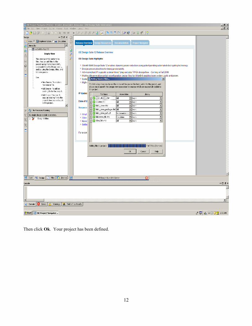
Click Finish and then Add Source. Choose files for the project.
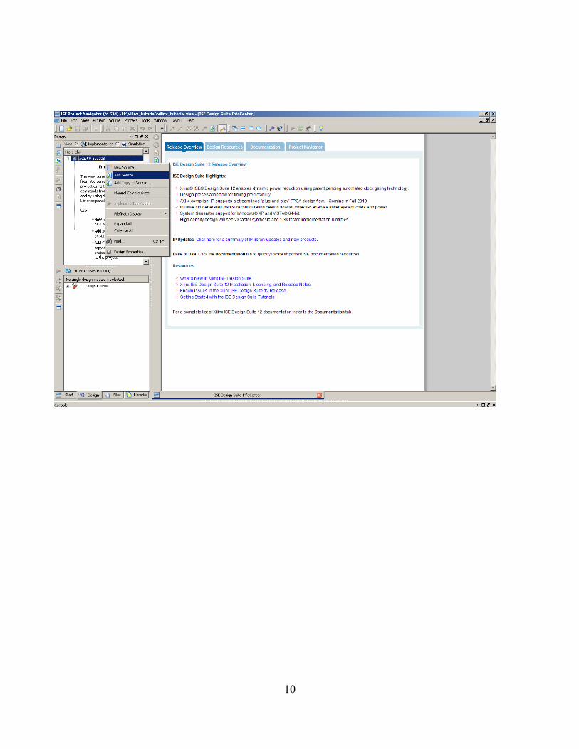
10

11
12
Then click Ok. Your project has been defined.
13
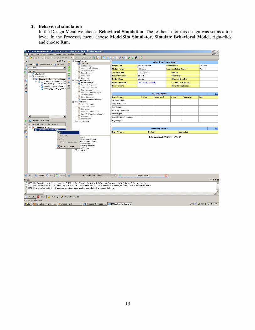
2. Behavioral simulation In the Design Menu we choose Behavioral Simulation. The testbench for this design was set as a top level. In the Processes menu choose ModelSim Simulator, Simulate Behavioral Model, right-click and choose Run.

14
You will see a picture similar to the one above.

15
Finally, you should be able to observe waveforms for your design.

16
3. Pin Assignment
Go to menu Sources for and change this option to Synthesis/Implementation. Click on Assign Package Pins. The User Constraint File (UCF) will be created if you decide to assign design port names to the physical pins. Columns I/O Names and I/O Descriptions represent ports from your design. The Loc column should be used to input the location of the corresponding pin in the FPGA device.

17

18
We can specify Pin Assignments by going to User Constraint menu. We can assign design port names to the physical pins of a chosen device by option Edit Constraints (Text). Keyword NET is for a port name assignment and keyword LOC is for a physical pin assignment.

19
4. Synthesis and Implementation 4.1 Synthesis with Xilinx XST Go to the menu Sources for and change this option to Synthesis/Implementation. Click Check Syntax to check if vhdl sources are properly coded.

20
When you right-click on Generate Post-Synthesis Simulation Model then pop-up menu appears. ChooseRun to start synthesis (There is no option to simulate post-synthesis netlist for Xilinx ISE WebPack). But you can see the post synthesis vhdl file in folder <project name>- <netgen><synthesis>

21
When Synthesis process is completed, the report from synthesis becomes available. Some of the most important features of the design are the minimum clock period and the maximum clock frequency. We can find these two parameters in the report file from Synthesis. Please remember that the values of these parameters after synthesis are different than the values of the same parameters after implementation.
The other important information we can find in this report is the amount of FPGA resources your design requires.

22
Synthesis and generation of Post-Synthesis Simulation Model were completed successfully and we can start Implementation part.

23
Implementation :

24
4.2 Translate The first step in the Xilinx Design Flow for implementation is Translate. Under Implement Design option, choose Translate, and then Run. If you are successful with this part you should generate Post Translate Simulation Model. 4.3 Post-Translate Simulation When you right-click on Generate Post-Translate Simulation Model then pop-up menu appears. Choose Run to start. In the menu Sources for we choose Post-Translate Simulation. The testbench for this design was set as a top level. In the menu Processes for choose ModelSim Simulator, right-click and choose Run.
ModelSim SE will be launched and waveforms for our design should appear. We can save script for further re-simulation by saving .do type files.

25
There is in the bottom part ModelSim terminal. We can type there commands such like do name_of_script.do and our waveform will be updated. It is possible to use terminal in every step of implementation. 4.4 Map Go to the menu Sources for and change this option to Synthesis/Implementation. From the Implement Design menu choose Map. Do right-click and pop-up menu should appear. Choose Run to start mapping process. Post-Map Simulation When you right-click on Generate Post-Map Simulation Model then pop-up menu appears. Choose Run to start. In the menu Sources for we choose Post-Map Simulation. The testbench for this design was set as a top level. In the menu Processes for choose ModelSim Simulator, right-click and choose Run.

26
4.5 Place and Route Go to menu Sources for and change this option to Synthesis/Implementation. From the Implement
Design menu choose Place and Route. Do right-click and pop-up menu should appear. Choose Run to start place and route process. When we right-click on Generate Post Place and Route Simulation Model then pop-up menu appears and you should choose Run.
27
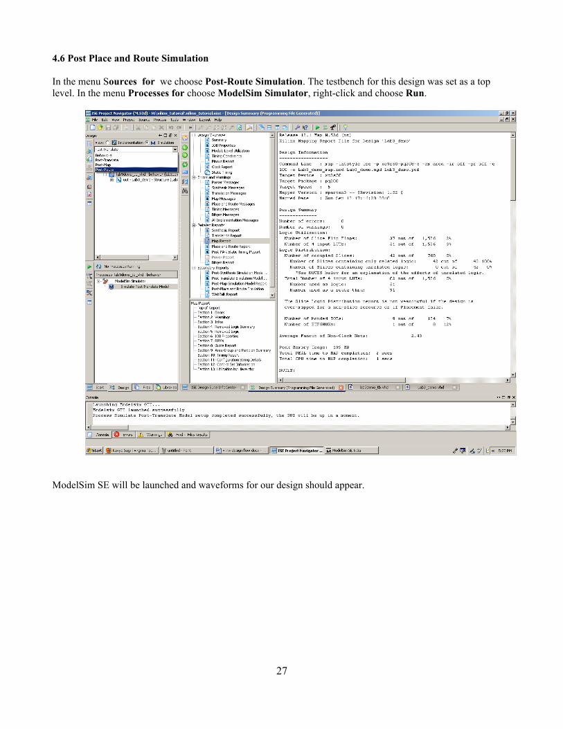
4.6 Post Place and Route Simulation In the menu Sources for we choose Post-Route Simulation. The testbench for this design was set as a top level. In the menu Processes for choose ModelSim Simulator, right-click and choose Run.
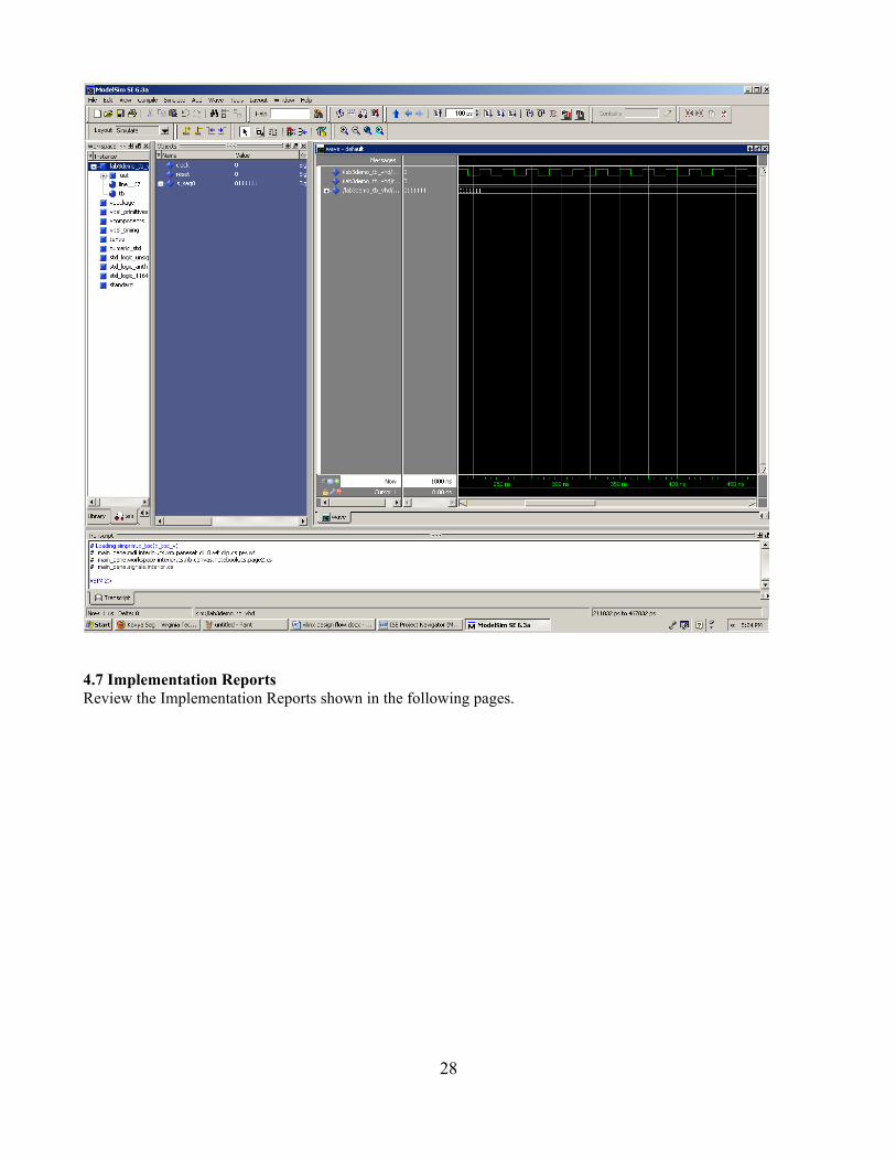
ModelSim SE will be launched and waveforms for our design should appear.
28
4.7 Implementation Reports Review the Implementation Reports shown in the following pages.

29

30

31
.

32
4.8 Bit Stream Generation
Go to menu Sources for and change this option to Synthesis/Implementation. Choose Generate Programming File, do right-click and pop-up menu should appear. Choose Run to start bit generation process.
33
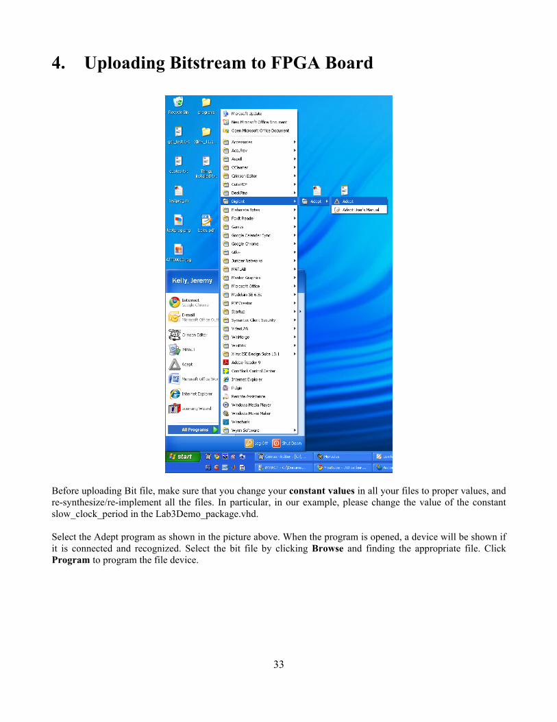
4. Uploading Bitstream to FPGA Board
Before uploading Bit file, make sure that you change your constant values in all your files to proper values, and re-synthesize/re-implement all the files. In particular, in our example, please change the value of the constant slow_clock_period in the Lab3Demo_package.vhd. Select the Adept program as shown in the picture above. When the program is opened, a device will be shown if it is connected and recognized. Select the bit file by clicking Browse and finding the appropriate file. Click Program to program the file device.

34
Good luck! Have fun debugging =)