Embed Size (px)
Citation preview

Tutorial II:
- Periodic Density Functional Theory Simulations
Solids and Surfaces
FHI-aims workshop
June 24, 2009
Paula Havu and Mina Yoon
Objectives of This Tutorial
o Periodic boundary conditions with DFT
o Cohesive properties of solids
o Basic properties of surfaces
o Electronic band structures & density of states

�r�R
exp(i�G ·�R) = 1
DFT with Periodic Boundary Conditions
Bravais lattice, a1,2,3: primitive vectors : integers
o Bloch theorem:
a1
a2
o Reciprocal lattice:
, where
Real space Reciprocal space
�k�G
�r�R
DFT with Periodic Boundary Conditions
Bravais lattice, a1,2,3: primitive vectors : integers
o Bloch theorem:
a1
a2
o Reciprocal lattice:
, where
Real space Reciprocal space
First Brillouin Zone
�k�G
exp(i�G ·�R) = 1

DFT with Periodic Boundary Conditions
Bravais lattice, a1,2,3: primitive vectors : integers
oBloch theorem:
a1
a2
o Reciprocal lattice:
, where
o KS equation : k-dependento Block like generalized basis function:
o ex: electron density
exp(i�G ·�R) = 1
Primitive Unit Cell vs. Brillouin Zone
Primitive fcc unit cellReal Space
Brillouin ZoneReciprocal Space
geometry.in (fcc Si, a=3.8Å):
lattice_vector 0.0 1.9 1.9lattice_vector 1.9 0.0 1.9lattice_vector 1.9 1.9 0.0
a

Silicon: fcc vs. diamond
•Diamond (=fcc with a basis)
Primitive unit cellReal Space
geometry.in (fcc Si, a=3.8Å):
lattice_vector 0.0 1.9 1.9lattice_vector 1.9 0.0 1.9lattice_vector 1.9 1.9 0.0 atom 0.0 0.0 0.0 Si
geometry.in (diamond Si a=5.4Å):
lattice_vector 0.0 2.7 2.7lattice_vector 2.7 0.0 2.7lattice_vector 2.7 2.7 0.0
atom 0.0 0.0 0.0 Siatom 1.35 1.35 1.35 Si
aa
•fcc
a
Convergence Test: Number of k-points
•Metallic example: fcc Si
•Semiconductor example: Diamond Si
Monkhorst-Pack grid(shift of k-grid by 0.5,0.5,0.5)
Monkhorst-Pack grid(shift of k-grid by 0.5,0.5,0.5)
(shift of k grid by 0.5,0.5,0.5)
(shift of k grid by 0.5,0.5,0.5)

Energy Convergence: Structural Stability
Small number of k-points:
Fcc< bcc < diamond
Sufficient number of k-points:
Diamond < bcc < fcc
Cohesive properties of solids
How to evaluate cohesive properties of solids?Birch-Murnaghan equation of states
Unit cell volume (V)
Tota
l ene
rgy
(E)
From elasticity theory, deformation of an isotropic medium
V: volumeV0: optimum volumeB0: bulk modulusB0’: derivative of B0 (w.r.t. pressure)E0: equilibrium energy
Cohesive energy:
E(V ) = E0 +B0VB′
0
((V0/V )B′
0
B′0−1
+1
)− B0V0
B′0−1
Ecoh = −Ebulk−N ×Eatom
N

Formation of Electronic Bands: Si (Diamond)
1s
2s
2p
3s
3p
4s3d
Ener
gy le
vel
atom (dSi-Si >> 1)
hybridization
solid
antibonding
bonding
Egap
Electronic Band of Diamond Si
[001]
[100]
[111]
[010]
[111] [100]
Valence band
Conduction band
Note: This is LDA results, which underestimatethe experimental gap of 1.17 eV,
Si is an indirect gap semiconductor
X
X
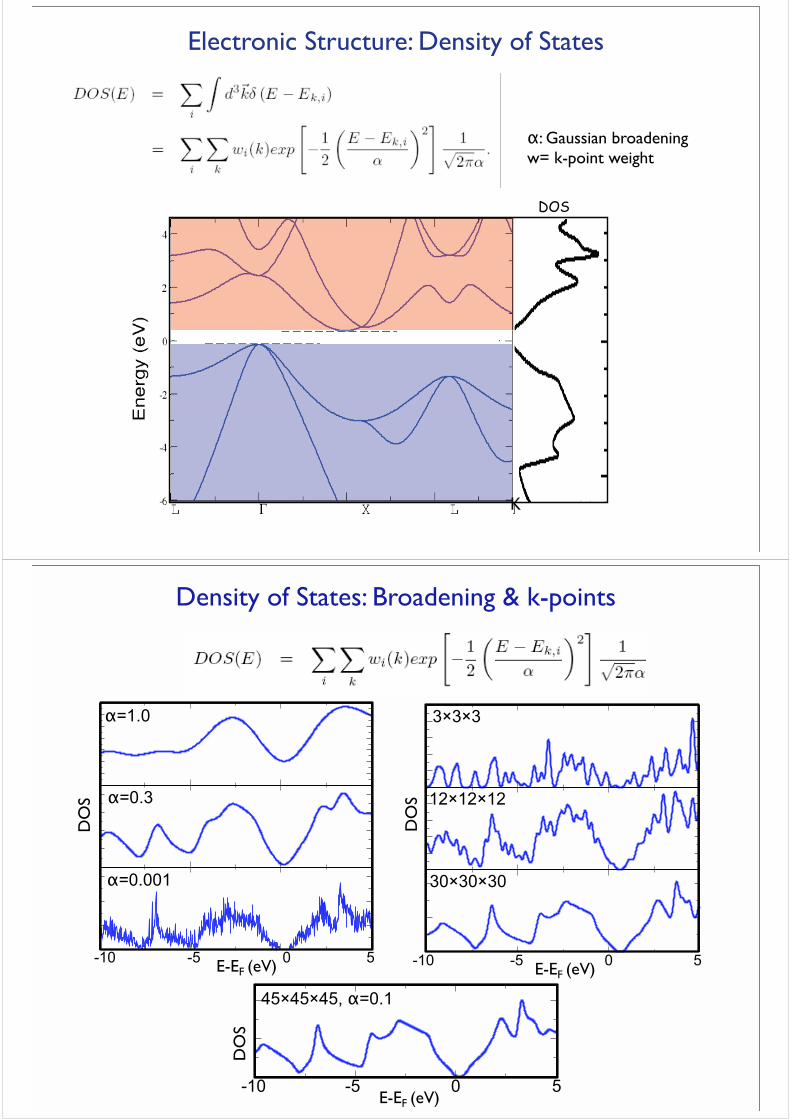
�: Gaussian broadening w= k-point weight
Electronic Structure: Density of States
K
DOS
Density of States: Broadening & k-points
E-EF (eV)
45�45�45, �=0.1
DO
S
0 5-5-10
DO
S
E-EF (eV) 0 5-5-10
3�3�3
12�12�12
30�30�30
�=1.0
�=0.3
�=0.001
E-EF (eV) 0 5-5-10
DO
S

Surface structure
truncated bulk geometry
formation of dimers
dimer buckling
alternating buckling
Example: different Si(100) surface geometries
0
4
2
-2
-4
0
4
2
-2
-4
Energ
y (
eV
)
� �J JK K
Surface band structure
Si truncated bulk geometry Si 2x2 surface reconstruction

Construction of Surfaces: Si(100) surface
Surface: Semi-infinite solid
Slab
supercell
(100)
(010)
(111)
(000)
Construction of “slab”
Vacuum
Convergence of Supercell Parameters
o Two new convergence parameters: vacuum length & number of atom layerso Reconstruction of Si(100) will be discussed in the Tutorial V.
Tips & Tricks: o Unphysical interactions between unsaturated charges on the top & bottom surface can be prevented by saturating with H (Tutorial V).o Dipole layer correction
Number of atom layersin slab Vacuum layer thickness (Å)
2 6 10 16
E / a
tom
[eV
]
-7847.104
-7847.112
-7847.108
Here: Basis set overlap
bulk

Esur f =Eslab−N ×Ebulk
2A
Eslab(N) = 2A×Esur f −N ×Ebulk
Energy required to create an unit area of surface:
How to calculate the reference energy (bulk energy)?
3) Apple to apple:
k x k x 1 k x k x 4
Different symmetry from surfaceBulk+surface need to be convergedWith k-mesh
1) bulk:
2) fitting:
Surface Energy
Overview
Part III: Basic properties of Si(100) surfaces
oGeneration & visualization of surfaces
oSurface band structures & surface energy
Part II: Electronic properties of bulk Si
oElectronic band structure& density of states
Part I: Basic properties of bulk Si & convergence test
oGeneration & visualization of bulk structures
oEnergy convergence tests
oRelative structural stability of different phases
oCohesive properties of bulk structures
Bonus problem!
Surface electronic structure of quantum thin films
2:30-3:10 (40min)
3:10-3:40 (30min)
3:40-4:10 (30min)
4:10-4:30 (20min)
5:00-5:20 (20min)
5:20-6:00 (40min)
2:30-4:30 (120min)
4:30-4:30 (30min)
5:00-6:00 (60min)


![Weka Inst Manual Boxcoolers 20090701[1]](https://img.pdfslide.us/doc/110x75/577ce09d1a28ab9e78b3b7df/weka-inst-manual-boxcoolers-200907011.jpg)