Embed Size (px)
Citation preview
UW-Madison: ECE 555/755 Cadence Tutorial-I Prepared By: Ranjith Kumar
TUTORIAL – I
CADENCE SCHEMATIC SIMULATION USING SPECTRE
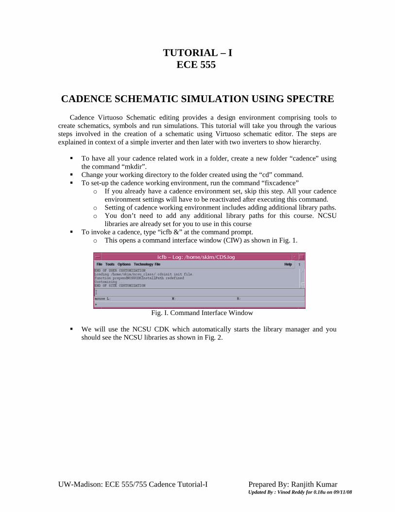
Cadence Virtuoso Schematic editing provides a design environment comprising tools to create schematics, symbols and run simulations. This tutorial will take you through the various steps involved in the creation of a schematic using Virtuoso schematic editor. The steps are explained in context of a simple inverter and then later with two inverters to show hierarchy.
To have all your cadence related work in a folder, create a new folder “cadence” using the command “mkdir”.
Change your working directory to the folder created using the “cd” command. To set-up the cadence working environment, run the command “fixcadence”
o If you already have a cadence environment set, skip this step. All your cadence environment settings will have to be reactivated after executing this command.
o Setting of cadence working environment includes adding additional library paths.o You don’t need to add any additional library paths for this course. NCSU
libraries are already set for you to use in this course To invoke a cadence, type “icfb &” at the command prompt.
o This opens a command interface window (CIW) as shown in Fig. 1.
Fig. I. Command Interface Window
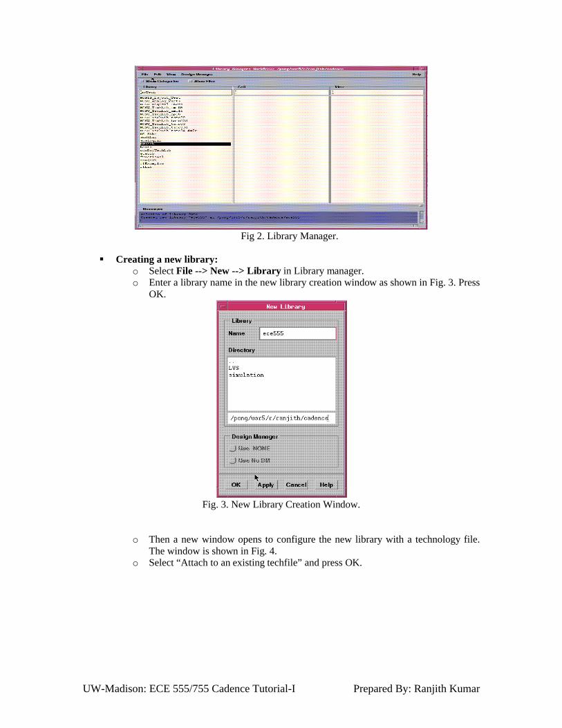
We will use the NCSU CDK which automatically starts the library manager and you should see the NCSU libraries as shown in Fig. 2.
ECE 555
Updated By : Vinod Reddy for 0.18u on 09/11/08
UW-Madison: ECE 555/755 Cadence Tutorial-I Prepared By: Ranjith Kumar
Fig 2. Library Manager.
Creating a new library: o Select File --> New --> Library in Library manager.o Enter a library name in the new library creation window as shown in Fig. 3. Press
OK.
Fig. 3. New Library Creation Window.
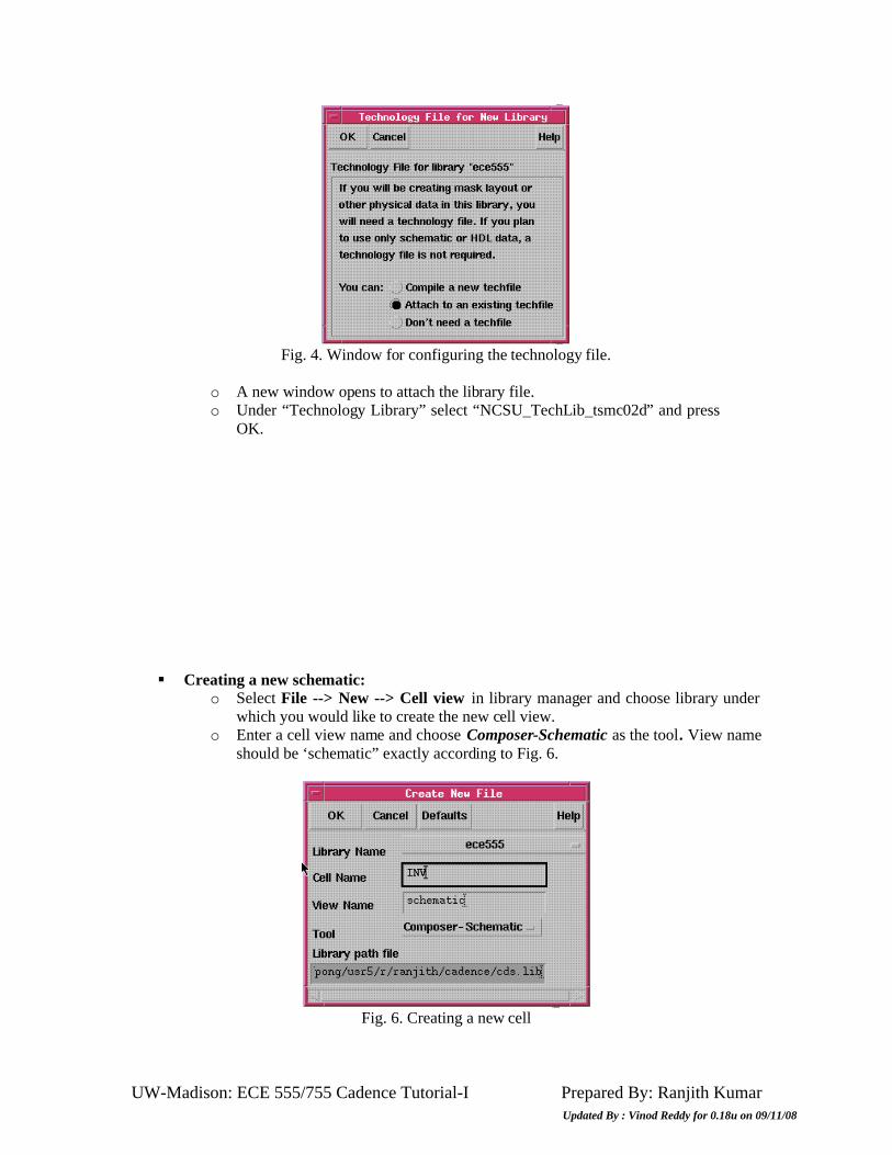
o Then a new window opens to configure the new library with a technology file. The window is shown in Fig. 4.
o Select “Attach to an existing techfile” and press OK.
UW-Madison: ECE 555/755 Cadence Tutorial-I Prepared By: Ranjith Kumar
Fig. 4. Window for configuring the technology file.
OK.
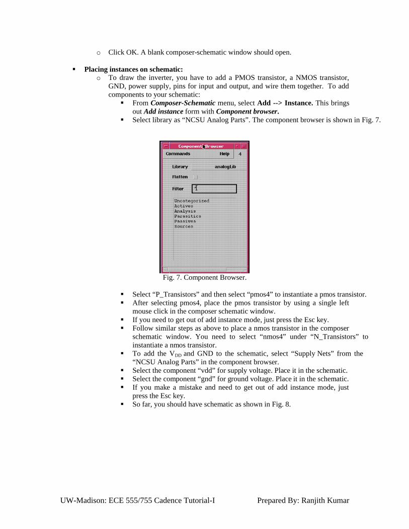
Creating a new schematic:o Select File --> New --> Cell view in library manager and choose library under
which you would like to create the new cell view.o Enter a cell view name and choose Composer-Schematic as the tool. View name
should be ‘schematic” exactly according to Fig. 6.
Fig. 6. Creating a new cell
o Under “Technology Library” select “NCSU_TechLib_tsmc02d” and press o A new window opens to attach the library file.
Updated By : Vinod Reddy for 0.18u on 09/11/08
UW-Madison: ECE 555/755 Cadence Tutorial-I Prepared By: Ranjith Kumar
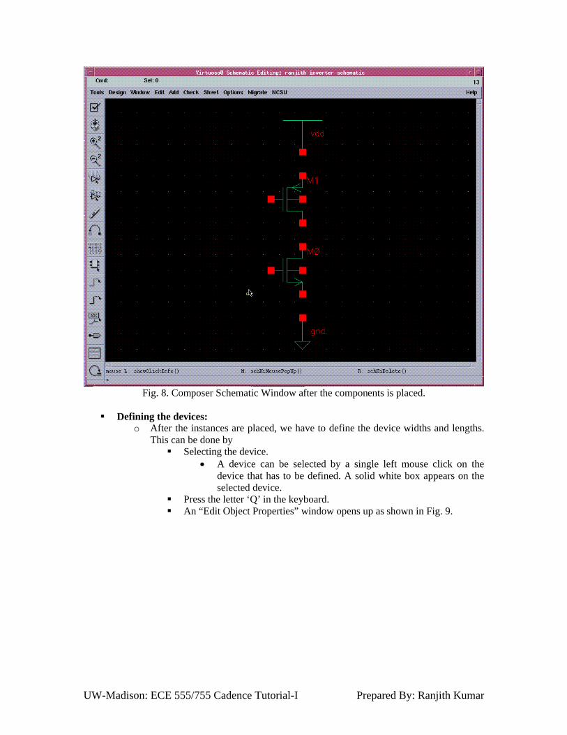
o Click OK. A blank composer-schematic window should open.
Placing instances on schematic: o To draw the inverter, you have to add a PMOS transistor, a NMOS transistor,
GND, power supply, pins for input and output, and wire them together. To add components to your schematic: From Composer-Schematic menu, select Add --> Instance. This brings
out Add instance form with Component browser.
Fig. 7. Component Browser.
After selecting pmos4, place the pmos transistor by using a single left mouse click in the composer schematic window.
If you need to get out of add instance mode, just press the Esc key. Follow similar steps as above to place a nmos transistor in the composer
instantiate a nmos transistor.DD
Select the component “vdd” for supply voltage. Place it in the schematic. Select the component “gnd” for ground voltage. Place it in the schematic. If you make a mistake and need to get out of add instance mode, just
press the Esc key. So far, you should have schematic as shown in Fig. 8.
Select library as “NCSU Analog Parts”. The component browser is shown in Fig. 7.
Select “P_Transistors” and then select “pmos4” to instantiate a pmos transistor.
schematic window. You need to select “nmos4” under “N_Transistors” to
To add the V and GND to the schematic, select “Supply Nets” from the “NCSU Analog Parts” in the component browser.
UW-Madison: ECE 555/755 Cadence Tutorial-I Prepared By: Ranjith Kumar
Fig. 8. Composer Schematic Window after the components is placed.
Defining the devices:o After the instances are placed, we have to define the device widths and lengths.
This can be done by Selecting the device.
A device can be selected by a single left mouse click on the device that has to be defined. A solid white box appears on the selected device.
Press the letter ‘Q’ in the keyboard. An “Edit Object Properties” window opens up as shown in Fig. 9.

UW-Madison: ECE 555/755 Cadence Tutorial-I Prepared By: Ranjith Kumar
Fig. 9. Edit object properties window.
width. Press OK.
width. Press OK.
After defining the devices, you should have schematic as Fig. 10.
For a PMOS, select model name as ‘tsmc18dP’ and define its length and
For a NMOS, select model name as ‘tsmc18dN’ and define its length and
The minimum width for the devices in this technology is 27 0nm.
The minimum length for the devices in this technology is 18 0nm.
UW-Madison: ECE 555/755 Cadence Tutorial-I Prepared By: Ranjith Kumar
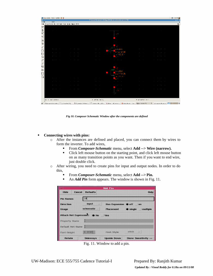
Connecting wires with pins: o After the instances are defined and placed, you can connect them by wires to
form the inverter. To add wires, From Composer-Schematic menu, select Add --> Wire (narrow). Click left mouse button on the starting point, and click left mouse button
on as many transition points as you want. Then if you want to end wire, just double click.
o After wiring, you need to create pins for input and output nodes. In order to do this, From Composer-Schematic menu, select Add --> Pin. An Add Pin form appears. The window is shown in Fig. 11.
Fig. 11. Window to add a pin.
Fig 10. Composer Schematic Window after the components are defined
Updated By : Vinod Reddy for 0.18u on 09/11/08
UW-Madison: ECE 555/755 Cadence Tutorial-I Prepared By: Ranjith Kumar
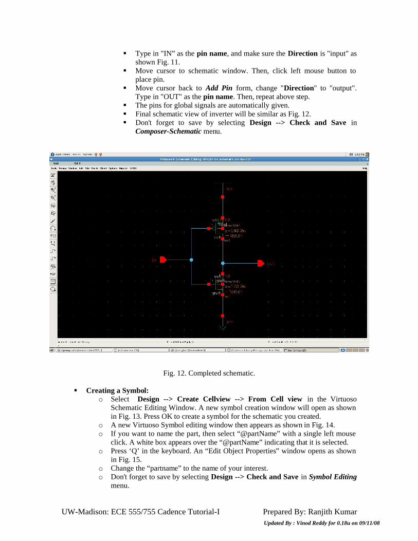
Type in "IN” as the pin name, and make sure the Direction is "input" as shown Fig. 11.
Move cursor to schematic window. Then, click left mouse button to place pin.
Move cursor back to Add Pin form, change "Direction" to "output". Type in "OUT" as the pin name. Then, repeat above step.
The pins for global signals are automatically given. Final schematic view of inverter will be similar as Fig. 12. Don't forget to save by selecting Design --> Check and Save in
Composer-Schematic menu.
Fig. 12. Completed schematic.
Creating a Symbol: o Select Design --> Create Cellview --> From Cell view in the Virtuoso
Schematic Editing Window. A new symbol creation window will open as shown in Fig. 13. Press OK to create a symbol for the schematic you created.
o A new Virtuoso Symbol editing window then appears as shown in Fig. 14. o If you want to name the part, then select “@partName” with a single left mouse
click. A white box appears over the “@partName” indicating that it is selected. o Press ‘Q’ in the keyboard. An “Edit Object Properties” window opens as shown
in Fig. 15.o Change the “partname” to the name of your interest.o Don't forget to save by selecting Design --> Check and Save in Symbol Editing
menu.
Updated By : Vinod Reddy for 0.18u on 09/11/08

UW-Madison: ECE 555/755 Cadence Tutorial-I Prepared By: Ranjith Kumar
Fig. 13. Creating a Symbol
Fig. 14. Virtuoso Symbol Editing Window.
Fig. 15. Edit Object Properties Window
UW-Madison: ECE 555/755 Cadence Tutorial-I Prepared By: Ranjith Kumar
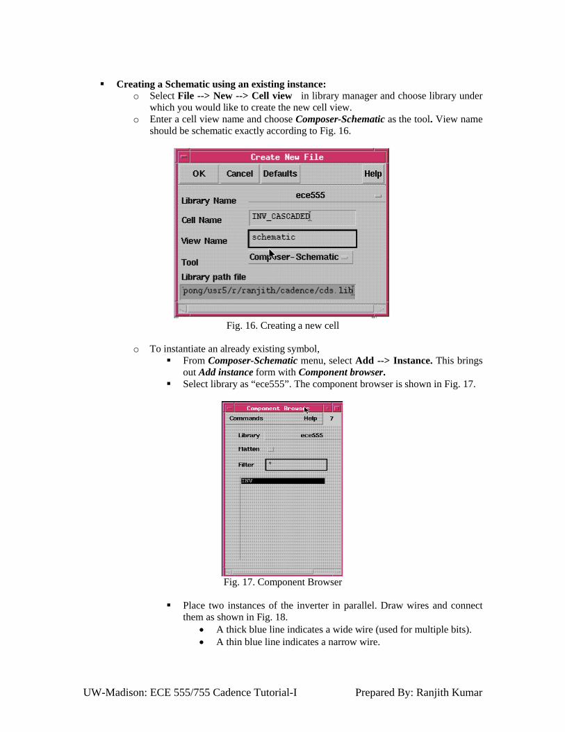
Creating a Schematic using an existing instance:o Select File --> New --> Cell view in library manager and choose library under
which you would like to create the new cell view.o Enter a cell view name and choose Composer-Schematic as the tool. View name
should be schematic exactly according to Fig. 16.
Fig. 16. Creating a new cell
o To instantiate an already existing symbol, From Composer-Schematic menu, select Add --> Instance. This brings
out Add instance form with Component browser. Select library as “ece555”. The component browser is shown in Fig. 17.
Fig. 17. Component Browser
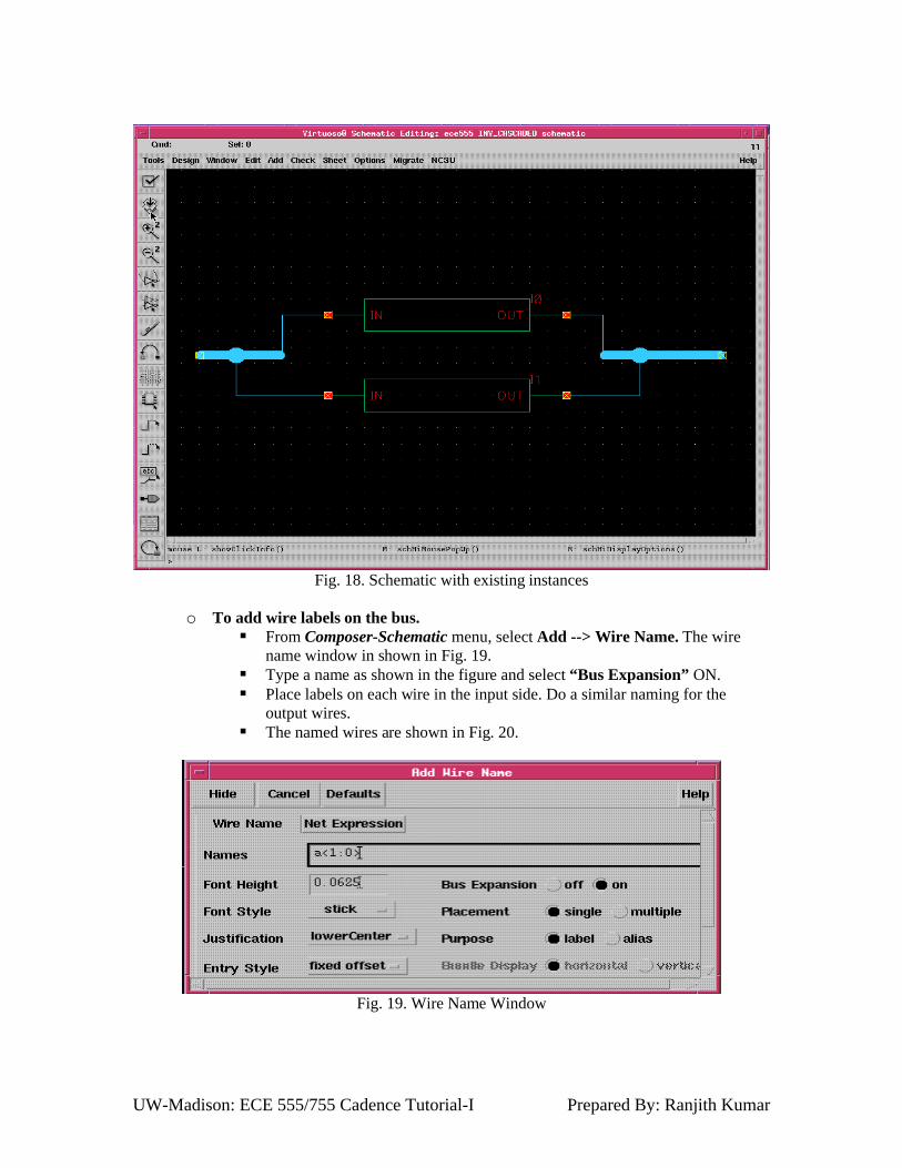
Place two instances of the inverter in parallel. Draw wires and connect them as shown in Fig. 18.
A thick blue line indicates a wide wire (used for multiple bits). A thin blue line indicates a narrow wire.
UW-Madison: ECE 555/755 Cadence Tutorial-I Prepared By: Ranjith Kumar
Fig. 18. Schematic with existing instances
o To add wire labels on the bus. From Composer-Schematic menu, select Add --> Wire Name. The wire
name window in shown in Fig. 19. Type a name as shown in the figure and select “Bus Expansion” ON. Place labels on each wire in the input side. Do a similar naming for the
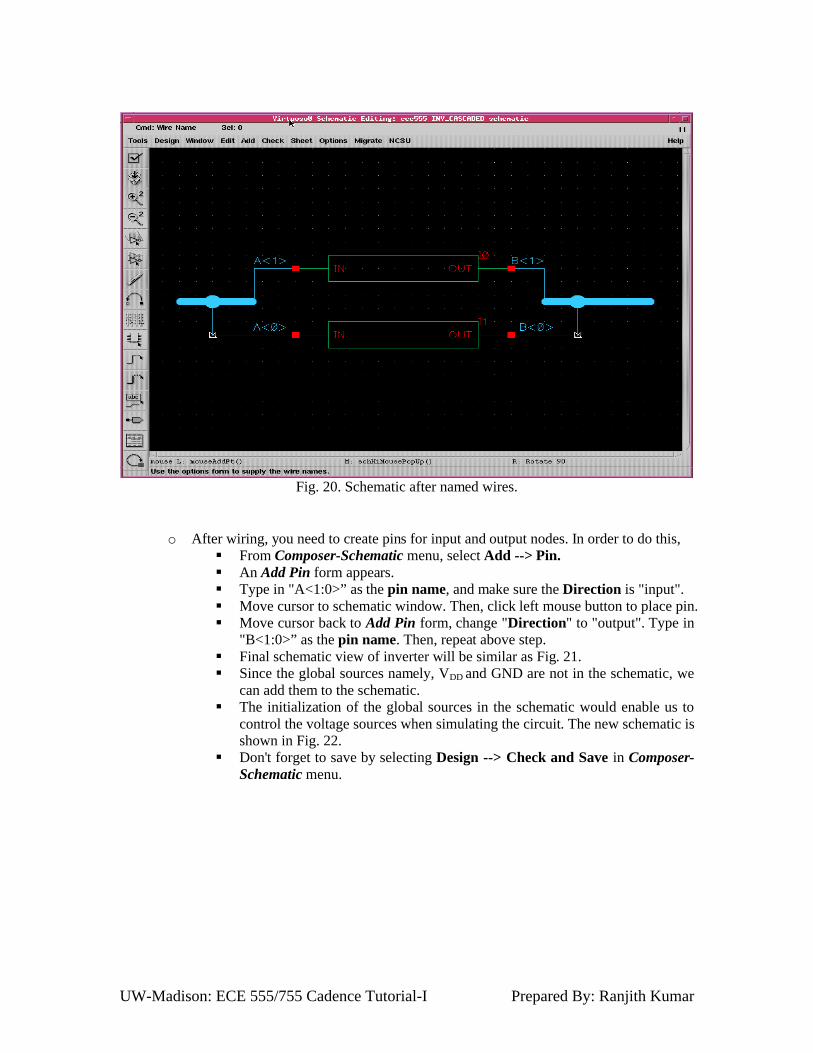
output wires. The named wires are shown in Fig. 20.
Fig. 19. Wire Name Window
UW-Madison: ECE 555/755 Cadence Tutorial-I Prepared By: Ranjith Kumar
o After wiring, you need to create pins for input and output nodes. In order to do this, From Composer-Schematic menu, select Add --> Pin. An Add Pin form appears. Type in "A<1:0>” as the pin name, and make sure the Direction is "input". Move cursor to schematic window. Then, click left mouse button to place pin. Move cursor back to Add Pin form, change "Direction" to "output". Type in
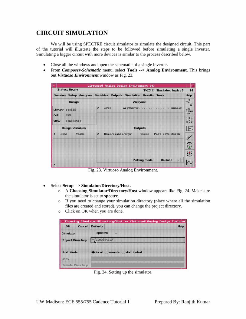
"B<1:0>” as the pin name. Then, repeat above step. Final schematic view of inverter will be similar as Fig. 21. Since the global sources namely, VDD and GND are not in the schematic, we
can add them to the schematic. The initialization of the global sources in the schematic would enable us to
control the voltage sources when simulating the circuit. The new schematic is shown in Fig. 22.
Don't forget to save by selecting Design --> Check and Save in Composer-Schematic menu.
Fig. 20. Schematic after named wires.
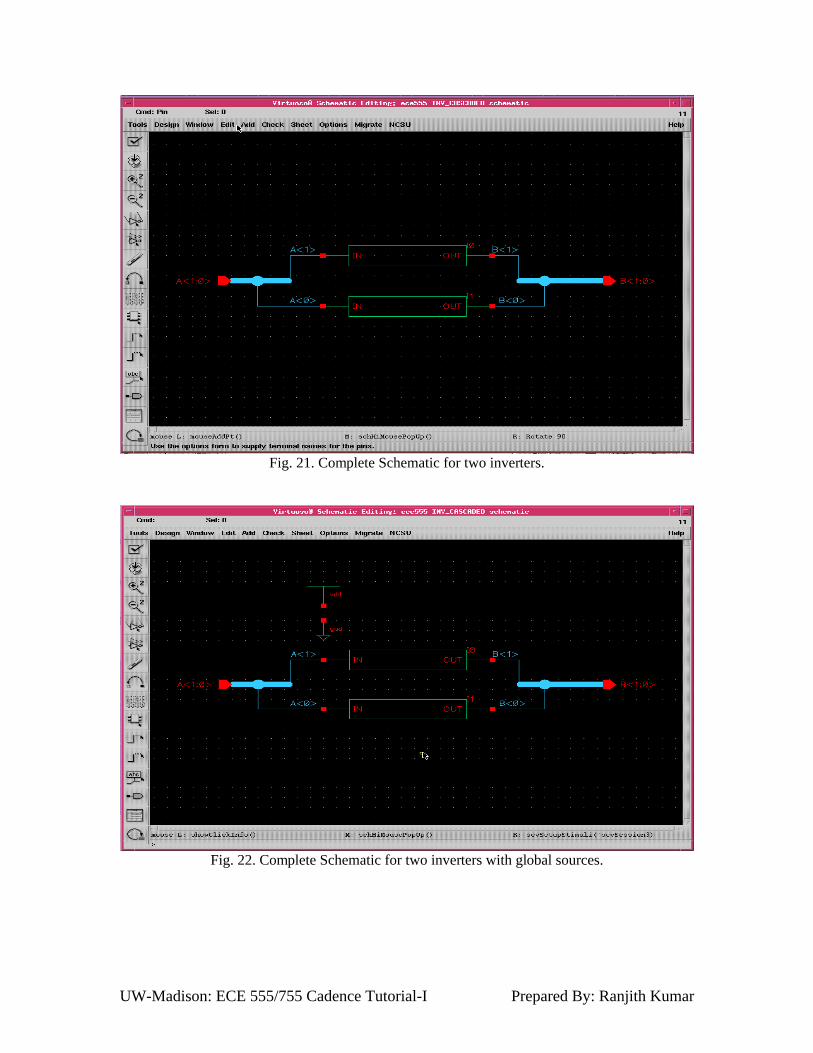
UW-Madison: ECE 555/755 Cadence Tutorial-I Prepared By: Ranjith Kumar
Fig. 21. Complete Schematic for two inverters.
Fig. 22. Complete Schematic for two inverters with global sources.
UW-Madison: ECE 555/755 Cadence Tutorial-I Prepared By: Ranjith Kumar
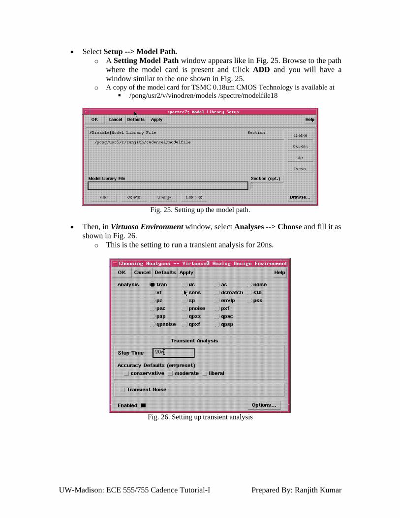
CIRCUIT SIMULATION
We will be using SPECTRE circuit simulator to simulate the designed circuit. This part of the tutorial will illustrate the steps to be followed before simulating a single inverter. Simulating a bigger circuit with more devices is similar to the process described below.
Close all the windows and open the schematic of a single inverter. From Composer-Schematic menu, select Tools --> Analog Environment. This brings
out Virtuoso Environment window as Fig. 23.
Fig. 23. Virtuoso Analog Environment.
Select Setup --> Simulator/Directory/Host.o A Choosing Simulator/Directory/Host window appears like Fig. 24. Make sure
the simulator is set to spectre.o If you need to change your simulation directory (place where all the simulation
files are created and stored), you can change the project directory.o Click on OK when you are done.
Fig. 24. Setting up the simulator.
UW-Madison: ECE 555/755 Cadence Tutorial-I Prepared By: Ranjith Kumar
Select Setup --> Model Path.o A Setting Model Path window appears like in Fig. 25. Browse to the path
where the model card is present and Click ADD and you will have a window similar to the one shown in Fig. 25.
Fig. 25. Setting up the model path.
Then, in Virtuoso Environment window, select Analyses --> Choose and fill it as shown in Fig. 26.
o This is the setting to run a transient analysis for 20ns.
Fig. 26. Setting up transient analysis
o A copy of the model card for TSMC 0.18um CMOS Technology is available at /pong/usr2/v/vinodren/models /spectre/modelfile18

UW-Madison: ECE 555/755 Cadence Tutorial-I Prepared By: Ranjith Kumar
In Virtuoso Environment window, select Outputs --> To Be Plotted --> Select On Schematic.
o Then, go back to schematic and click on the wires attached input and output of inverter. The wires should change colors. Press Esc key to exit of selection mode. The signals should be added in the outputs window, as shown in Fig. 27.
Fig. 27. Setting up the output plots.
Select Setup --> Stimuli.o A Setting Analog Stimuli window appears like in Fig. 28.o To set-up a input pulse at the pin “IN”
Select Stimulus Type “Inputs” Check “Enable” Set “function” to “pulse” Set “Voltage 1” to 0.0
Set “Delay time” to 0
Press “Change”o To set-up a global inputs
Select Stimulus Type “Global Sources” Check “Enable” Set “function” to “dc”
Press “Change”o Press OKo In Virtuoso Environment window, select Simulation --> Run.
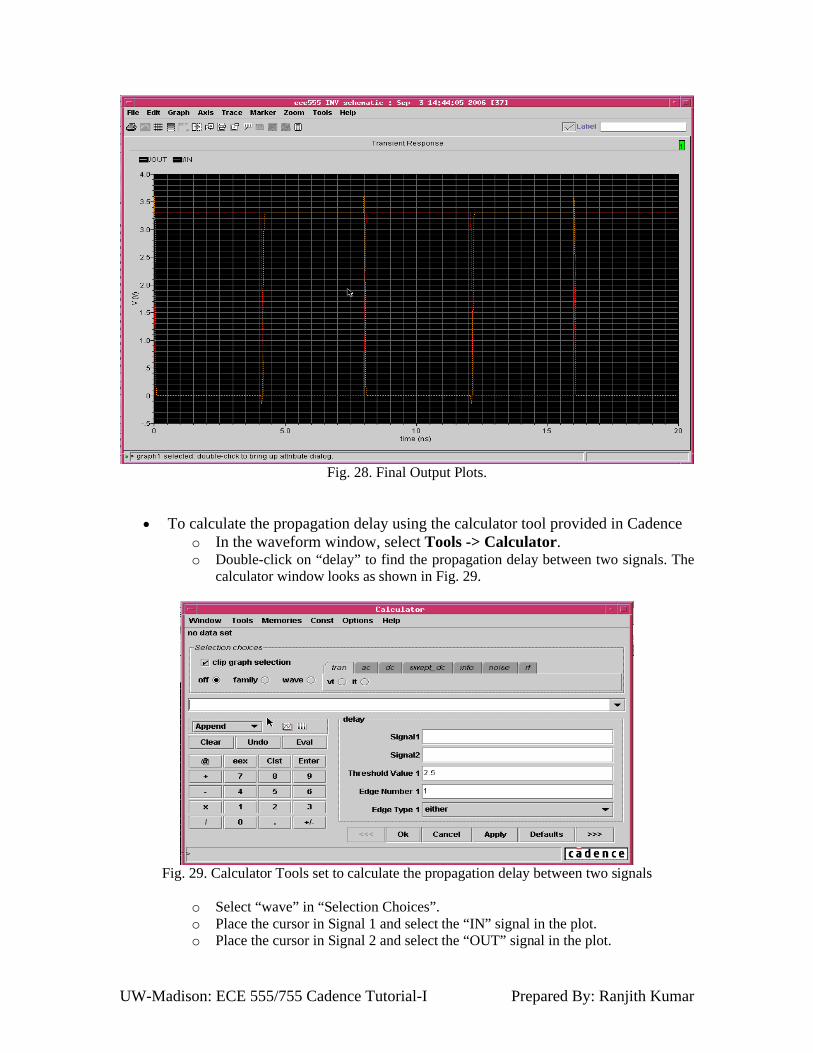
The plot of the simulation should appear in the Waveform Window, similar to Fig. 28.
Set “Voltage 2” to 1.8
Set “Rise Time” to 0.05n Set “Fall Time” to 0.05n Set “Pulse Width” to 2n Set “Period” to 4n
Set DC Voltage to 1.8V
UW-Madison: ECE 555/755 Cadence Tutorial-I Prepared By: Ranjith Kumar
Fig. 28. Final Output Plots.
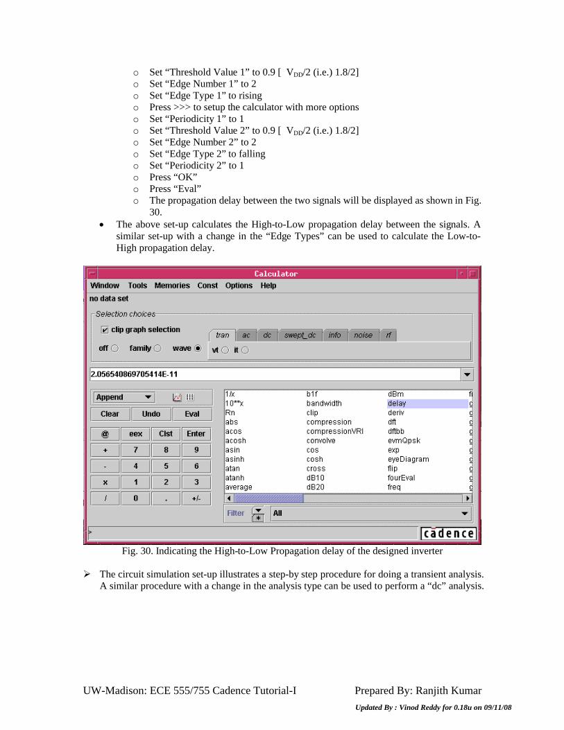
To calculate the propagation delay using the calculator tool provided in Cadenceo In the waveform window, select Tools -> Calculator.o Double-click on “delay” to find the propagation delay between two signals. The
calculator window looks as shown in Fig. 29.
Fig. 29. Calculator Tools set to calculate the propagation delay between two signals
o Select “wave” in “Selection Choices”.o Place the cursor in Signal 1 and select the “IN” signal in the plot.o Place the cursor in Signal 2 and select the “OUT” signal in the plot.
UW-Madison: ECE 555/755 Cadence Tutorial-I Prepared By: Ranjith Kumar
DD
o Set “Edge Number 1” to 2o Set “Edge Type 1” to risingo Press >>> to setup the calculator with more optionso Set “Periodicity 1” to 1
DD
o Set “Edge Number 2” to 2o Set “Edge Type 2” to fallingo Set “Periodicity 2” to 1o Press “OK”o Press “Eval”o The propagation delay between the two signals will be displayed as shown in Fig.
30. The above set-up calculates the High-to-Low propagation delay between the signals. A
similar set-up with a change in the “Edge Types” can be used to calculate the Low-to-High propagation delay.
Fig. 30. Indicating the High-to-Low Propagation delay of the designed inverter
The circuit simulation set-up illustrates a step-by step procedure for doing a transient analysis. A similar procedure with a change in the analysis type can be used to perform a “dc” analysis.
o Set “Threshold Value 1” to 0.9 [ V /2 (i.e.) 1.8/2]
o Set “Threshold Value 2” to 0.9 [ V /2 (i.e.) 1.8/2]
Updated By : Vinod Reddy for 0.18u on 09/11/08

UW-Madison: ECE 555/755 Cadence Tutorial-I Prepared By: Ranjith Kumar
SIMULATION OF LARGE CIRCUITS
We can follow the above procedure to simulating large circuits. However, as the number of stimuli increases, the time to set the stimuli values also increases. In this section of the tutorial, you will be introduced to some techniques to save time while simulating large circuits with many stimuli values.
Technique I:The easiest option is to save the stimuli values that were entered once and reuse the state
values when needed consequently.
After all the stimuli values are entered for the first time in the Virtuoso Environment window, select Session -> Save State. A save state window appears as shown in Fig. 31.
Fig. 31. Save State Window
The stimuli values along with the analysis type, waveforms to plot, technology file path and other settings gets saved under the specified name.
When needed later, the state can be retrieved by selecting Session -> Load State in the Virtuoso Environment window after selecting the corresponding simulator.
UW-Madison: ECE 555/755 Cadence Tutorial-I Prepared By: Ranjith Kumar
Technique II:The other option is to write the stimuli in a file and add it to the simulation whenever
needed.
A sample stimulus file for the above inverter is given below A copy of the stimulus file is available at
V2 gnd! 0 0
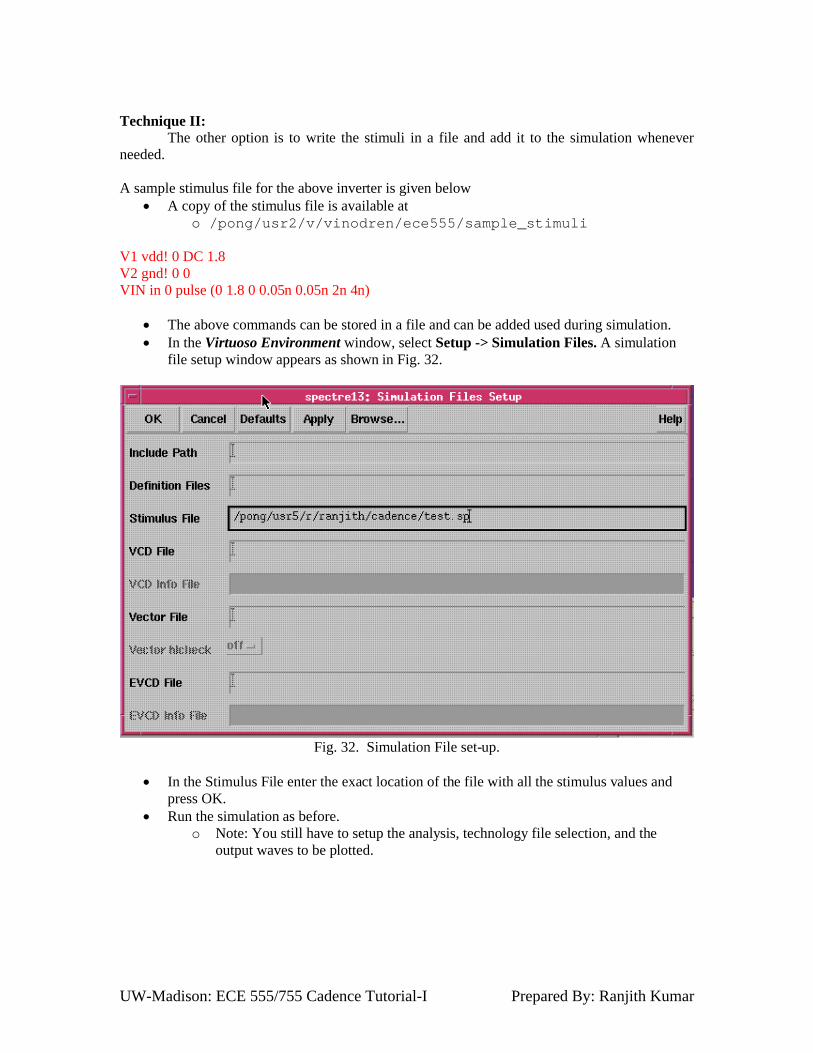
The above commands can be stored in a file and can be added used during simulation. In the Virtuoso Environment window, select Setup -> Simulation Files. A simulation
file setup window appears as shown in Fig. 32.
Fig. 32. Simulation File set-up.
In the Stimulus File enter the exact location of the file with all the stimulus values and press OK.
Run the simulation as before.o Note: You still have to setup the analysis, technology file selection, and the
output waves to be plotted.
V1 vdd! 0 DC 1.8
VIN in 0 pulse (0 1.8 0 0.05n 0.05n 2n 4n)
o /pong/usr2/v/vinodren/ece555/sample_stimuli

UW-Madison: ECE 555/755 Cadence Tutorial-I Prepared By: Ranjith Kumar
Syntax of some important statements
Pulse Signal: The definition of a pulse is as follows:pulse ( voltage_1 voltage_2 offset_time rise_time fall_time duty_cycle period)
cycle of 2n and a period of 4n
Piece-Wise Linear: The definition is as follows
pwl ( time1 voltage1 time2 voltage2 time3 voltage3 time4 voltage4…..)
interval 4ns to 4.1ns and remains stationary afterwards.
Ex: pulse( 0 1.8 0 0.05n 0.05n 2n 4n)
Produces a pulse from 0V to 1.8V with 0 offset and 0.05n rise and fall time with a duty
Ex: pwl ( 0 0 2n 0 2.1n 1.8 4n 1.8 4.1n 0)
Produces a signal that stays at 0v from time 0s to 2ns and then rises to 1.8volts in the time interval 2ns to 2.1ns and stays at 1.8v from 2.1n to 4ns and goes from 1.8v to 0v in the time
Updated By : Vinod Reddy for 0.18u on 09/11/08