Embed Size (px)
Citation preview
�1
Biosensors and Instrumentation: Tutorial 2 Solutions
1. One of the most straightforward methods of monitoring temperature is to use the thermal variation of a resistor. 1.1. Suggest a possible problem with the use of a standard Wheatstone bridge setup in a remote
application like an implanted sensor?The other resistors used in the bridge will also have some temperature dependence which will be confounded with that of the RTD if care is not taken. It would be very hard to control temperatures in an implanted device like that.
1.2. Can you suggest a possible solution?It is unlikely but if the temperature dependence of the other resistors can be made to be much much smaller than the measured device then this could almost be ignored.
1.3. The alternative might be to locate the resistor at the remote sensing position while the instrumentation is in a stable environment. Why does this lead to a problem?The resistance of the electrical connections to the RTD become a problem. These could be balanced at one particular temperature but they may also have some temperature dependence that will cause an error in the measurement.
1.4. Why does a Kelvin measurement improve measurements of small resistances?Current and voltage are separated in a four-terminal Kelvin measurement meaning that the resistance of the electrical connections should not impact on the measured resistance.
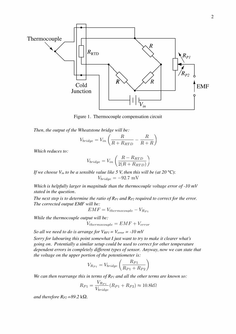
2. The circuit shown in figure 1 can be used to compensate for the error in the output voltage which results from the fact that the “cold junction” is not at 0 ℃. There are two parameters which can control this compensation (assuming all of the resistors in the Wheatstone bridge are equal when the cold bridge temperature is 0 ℃), which are the voltage used to power the bridge and the position of the potentiometer. If we have the following parameters suggest values for Vin, and the ratio of RP1 to RP2 to correct for an observed error in the thermocouple output EMF of –10mV when the cold junction is at room temperature (20 ℃):
RRTD = 100 Ω @ Tjunction = 0 ℃αRTD = 0.00385 Ω Ω–1 K–1
R = 100 Ω (Wheatstone bridge resistor)RPot = RP1 + RP2 = 100 kΩ1
The first step in solving this is to determine the output of the Wheatstone bridge, which gives us the temperature dependent voltage which can then be used to correct for the error due to the cold junction temperature. The resistance RRTD at 20 ℃ is:
�RRTD = R0[1 + ↵(T � T0)] = 107.7 ⌦
Hint for Q2, if RRTD is greater than R then think about the size and direction of the voltage output from the 1
Wheatstone bridge then about how that adds/subtracts from the EMF from the thermocouple and the cold junctions in order to correct for any error. It might be useful to redraw the circuit with voltage sources replacing these components.
�2
�Figure 1. Thermocouple compensation circuit
Then, the output of the Wheatstone bridge will be:
�Which reduces to:
�If we choose Vin to be a sensible value like 5 V, then this will be (at 20 ℃):
�Which is helpfully larger in magnitude than the thermocouple voltage error of -10 mV stated in the question. The next step is to determine the ratio of RP1 and RP2 required to correct for the error. The corrected output EMF will be:
�While the thermocouple output will be:
�So all we need to do is arrange for VRP1 = Verror = -10 mVSorry for labouring this point somewhat I just want to try to make it clearer what’s going on. Potentially a similar setup could be used to correct for other temperature dependent errors in completely different types of sensor. Anyway, now we can state that the voltage on the upper portion of the potentiometer is:
�We can then rearrange this in terms of RP1 and all the other terms are known so:
�and therefore RP2 =89.2 kΩ.
EMF
RRTD
RR R
R
Vin
RP1
RP2
ColdJunction
Thermocouple
Vbridge = Vin
✓R
R+RRTD� R
R+R
◆
Vbridge = Vin
✓R�RRTD
2(R+RRTD)
◆
Vbridge = �92.7 mV
EMF = Vthermocouple
� VRP1
Vthermocouple
= EMF + Verror
VRP1 = Vbridge
✓RP1
RP1 +RP2
◆
RP1 =VRP1
Vbridge(RP1 +RP2) ⇡ 10.8k⌦
�3
3. The basic formula for resistance is R = ρ L/A. From this we can work out the fractional change in resistivity for a strain gauge:
" The first term there deals with the change in the material resistivity due to applied strain. The piezoresistive coefficient π is defined as:
�Where E is the Young’s modulus of the material and ε is the strain (ε = ΔL/L).Poisson’s ratio ν is another material parameter that defines the change in the transverse strain due to an applied axial strain, for our resistor we can say that:
�3.1. Combine all of this information with the equation for the gauge factor of a piezoresistor
(given below) to produce an expression for GF in terms of ν, π and E.
�Going back to the piezo resistive coefficient:
�Then using the formula for gauge factor:
�Finally we remember that strain is ε = ΔL/L and the formula for Poisson’s ratio given above and substitute where appropriate:
�
3.2. In most metals the poisson ratio is between 0 and 0.5, while the effect of π is negligible, what does that mean for the possible range of values for GF?With no significant piezoresistive effect the gauge factor will vary between 1 (for ν = 0) and 2 (for ν = 1).
3.3. Polycrystalline silicon can have a gauge factor as high as 40. What is the source of this?Semiconductors all have significant piezoresistive effects meaning that π dominates in the GF equation. The source of this is the effect of strain on the mobility of charge carriers in the semiconductor.
4. A platinum based strain gauge with an unstrained resistance (RG) of 1kΩ has a gauge factor (GF) of 2. The formula for gauge factor is covered in the previous question.
�R
R=
��
�� �A
A+
�L
L
� =�⇥/⇥
E⇤
�A/A
�L/L= �2�
GF =�R
�RG
�⇥
⇥= �E⇤
GF =1
⇥
✓��
�� �A
A+
�L
L
◆
GF = 1 + 2� + ⇥E
�4
4.1. If the gauge is securely fixed to a measured structure undergoing a strain (ε) of 10%, what will be the maximum change in resistance (∆R)?
�This is obviously quite large and reflects the rather unrealistically high strain value.
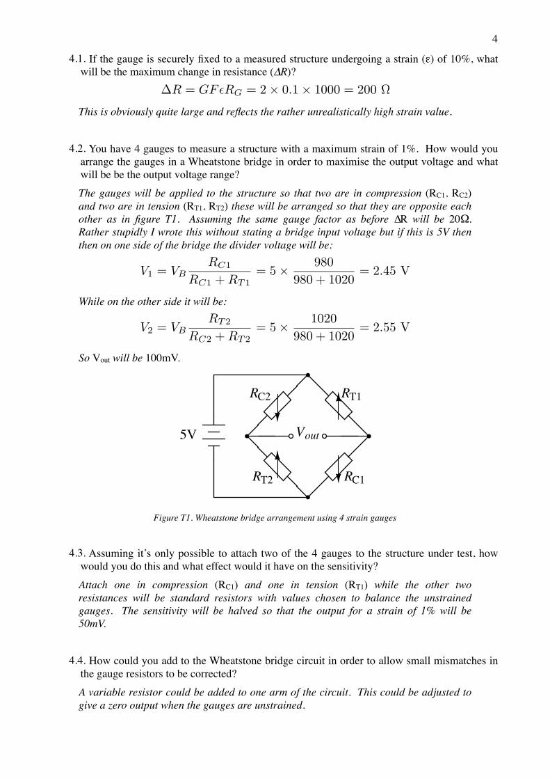
4.2. You have 4 gauges to measure a structure with a maximum strain of 1%. How would you arrange the gauges in a Wheatstone bridge in order to maximise the output voltage and what will be be the output voltage range?The gauges will be applied to the structure so that two are in compression (RC1, RC2) and two are in tension (RT1, RT2) these will be arranged so that they are opposite each other as in figure T1. Assuming the same gauge factor as before ∆R will be 20Ω. Rather stupidly I wrote this without stating a bridge input voltage but if this is 5V then then on one side of the bridge the divider voltage will be:
�While on the other side it will be:
�So Vout will be 100mV.
�Figure T1. Wheatstone bridge arrangement using 4 strain gauges
4.3. Assuming it’s only possible to attach two of the 4 gauges to the structure under test, how would you do this and what effect would it have on the sensitivity? Attach one in compression (RC1) and one in tension (RT1) while the other two resistances will be standard resistors with values chosen to balance the unstrained gauges. The sensitivity will be halved so that the output for a strain of 1% will be 50mV.
4.4. How could you add to the Wheatstone bridge circuit in order to allow small mismatches in the gauge resistors to be corrected?A variable resistor could be added to one arm of the circuit. This could be adjusted to give a zero output when the gauges are unstrained.
�R = GF ✏RG = 2⇥ 0.1⇥ 1000 = 200 ⌦
V1 = VBRC1
RC1 + RT1= 5⇥ 980
980 + 1020= 2.45 V
V2 = VBRT2
RC2 + RT2= 5⇥ 1020
980 + 1020= 2.55 V
V5V
RR
R R
T1
out
C1T2
C2
�5
5. Piezoelectric acoustic wave devices are now widely used in RF filters in mobile communications and in passive RF-ID tags. Surface acoustic wave filters can also be adapted into sensitive detectors. The frequency of the acoustic wave is proportional to the wave velocity in the material.5.1. Suggest how this could be used in a biosensor.
Biosensing molecules can be attached to the surface of the SAW sensor, changing the mass that is being moved by the wave, effectively changing the transmission velocity. Subsequent attachment of the chemical/marker being sensed will further change this and the change can be detected.
5.2. What factors can also affect the frequency?Temperature and applied strains can also affect the SAW frequency, by altering the wave velocity or by slightly changing the distance between the interdigitated electrodes.
5.3. How can these be corrected for? Sketch a SAW sensor setup that could avoid these problems which only uses one driven IDE.The RF pulse is fed to the central IDE which sends out SAW pulses in opposite directions. These are reflected back and the difference in timing between the pulse from the sensing and reference sides contains information about the status of the sensing area. Changes due to temperature or applied strain should be common for both sides of the sensor and can be cancelled out.
5.4. Why are “Rayleigh wave” type SAW devices unsuitable for use in liquid environments?Rayleigh waves have an amplitude that is normal to the surface of the SAW device and are heavily damped by contact with dense fluids. This could prevent the propagation of the SAW waves from the input transducer to the input.
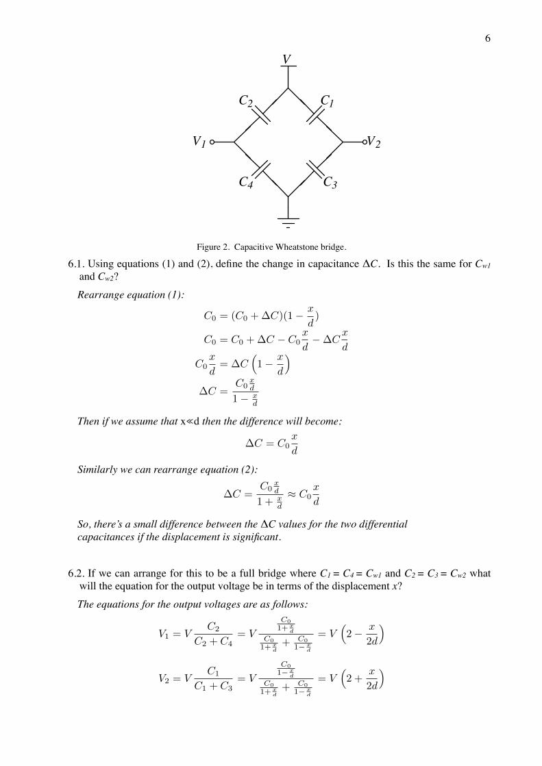
6. The capacitive bridge circuit shown in figure 2 is used to convert changes in the capacitance of a MEMS accelerometer with a differential sensing setup. It has the following output voltage amplitude, when driven with an ac voltage with amplitude V:
�When C2 = C4 = C0, C1 = Cw1 and C3 = Cw2 where
� (1)and
� (2)
V
out
= V2 � V1 = V
x
2d
Cw1 =
C0
1� x
d
= C0 +�C
Cw2 =
C0
1 + x
d
= C0 ��C
�6
�Figure 2. Capacitive Wheatstone bridge.
6.1. Using equations (1) and (2), define the change in capacitance ΔC. Is this the same for Cw1 and Cw2?Rearrange equation (1):
�Then if we assume that x≪d then the difference will become:
�Similarly we can rearrange equation (2):
�So, there’s a small difference between the ΔC values for the two differential capacitances if the displacement is significant.
6.2. If we can arrange for this to be a full bridge where C1 = C4 = Cw1 and C2 = C3 = Cw2 what will the equation for the output voltage be in terms of the displacement x?The equations for the output voltages are as follows:
�
�
V
C1C2
CC 34
V V1 2
C0 = (C0 +�C)(1� x
d
)
C0 = C0 +�C � C0x
d
��C
x
d
C0x
d
= �C
⇣1� x
d
⌘
�C =C0
x
d
1� x
d
�C = C0x
d
�C =C0
x
d
1 + x
d
⇡ C0x
d
V1 = V
C2
C2 + C4= V
C01+ x
d
C01+ x
d
+ C01� x
d
= V
⇣2� x
2d
⌘
V2 = V
C1
C1 + C3= V
C01� x
d
C01+ x
d
+ C01� x
d
= V
⇣2 +
x
2d
⌘
�7
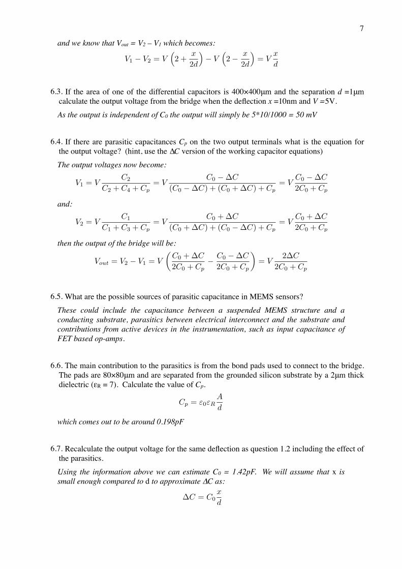
and we know that Vout = V2 – V1 which becomes:
�
6.3. If the area of one of the differential capacitors is 400×400μm and the separation d =1μm calculate the output voltage from the bridge when the deflection x =10nm and V =5V. As the output is independent of C0 the output will simply be 5*10/1000 = 50 mV
6.4. If there are parasitic capacitances Cp on the two output terminals what is the equation for the output voltage? (hint, use the ∆C version of the working capacitor equations)The output voltages now become:
�and:
�then the output of the bridge will be:
�
6.5. What are the possible sources of parasitic capacitance in MEMS sensors?These could include the capacitance between a suspended MEMS structure and a conducting substrate, parasitics between electrical interconnect and the substrate and contributions from active devices in the instrumentation, such as input capacitance of FET based op-amps.
6.6. The main contribution to the parasitics is from the bond pads used to connect to the bridge. The pads are 80×80μm and are separated from the grounded silicon substrate by a 2μm thick dielectric (εR = 7). Calculate the value of Cp.
� which comes out to be around 0.198pF
6.7. Recalculate the output voltage for the same deflection as question 1.2 including the effect of the parasitics.Using the information above we can estimate C0 = 1.42pF. We will assume that x is small enough compared to d to approximate ∆C as:
�
V1 � V2 = V
⇣2 +
x
2d
⌘� V
⇣2� x
2d
⌘= V
x
d
V1 = VC2
C2 + C4 + Cp= V
C0 ��C
(C0 ��C) + (C0 +�C) + Cp= V
C0 ��C
2C0 + Cp
V2 = VC1
C1 + C3 + Cp= V
C0 +�C
(C0 +�C) + (C0 ��C) + Cp= V
C0 +�C
2C0 + Cp
Vout
= V2 � V1 = V
✓C0 +�C
2C0 + Cp
� C0 ��C
2C0 + Cp
◆= V
2�C
2C0 + Cp
Cp = "0"RA
d
�C = C0x
d
�8
So ∆C = 14.2 fF and Vout = 0.04673V. It’s not a huge effect (<10%) but if Cp was ten times larger (~2pF), which isn’t unheard of then the output would only be about 0.03V, a change of 40%.
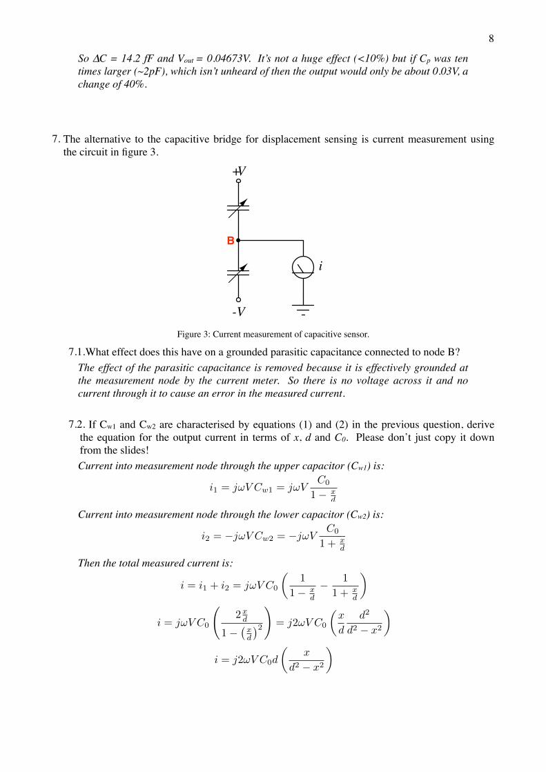
7. The alternative to the capacitive bridge for displacement sensing is current measurement using the circuit in figure 3.
�Figure 3: Current measurement of capacitive sensor.
7.1.What effect does this have on a grounded parasitic capacitance connected to node B?The effect of the parasitic capacitance is removed because it is effectively grounded at the measurement node by the current meter. So there is no voltage across it and no current through it to cause an error in the measured current.
7.2. If Cw1 and Cw2 are characterised by equations (1) and (2) in the previous question, derive the equation for the output current in terms of x, d and C0. Please don’t just copy it down from the slides!Current into measurement node through the upper capacitor (Cw1) is:
�Current into measurement node through the lower capacitor (Cw2) is:
�Then the total measured current is:
�
�
�
B
V
-V
+
i
i1 = j�V Cw1 = j�V
C0
1� x
d
i2 = �j�V Cw2 = �j�V
C0
1 + x
d
i = i1 + i2 = j�V C0
✓1
1� x
d
� 1
1 + x
d
◆
i = j�V C0
2x
d
1��x
d
�2
!= j2�V C0
✓x
d
d2
d2 � x2
◆
i = j2�V C0d
✓x
d2 � x2
◆
�9
7.3. If this circuit is used to measure a micromachined accelerometer with nominal gap d = 2.5 μm and area A = 1.2 mm × 1.2 mm calculate the output current when the displacement is 0.46 μm and the device is driven with an ac voltage V = 0.1 V, f = 100 kHz.First calculate C0 = 5.1pF then slot all the numbers into the equation to get i = 0.12µA.
7.4. If a current-follower op-amp circuit is used to amplify and convert this current, what value of resistor is required to give a 1V p-p voltage output?For a current follower Vout = -iR, so to get 1V from 0.12µA, R ≈ 8.2MΩ.
8. Switched capacitor circuits may be more appropriate for use in IC based sensor interfaces.8.1. Give as many reasons as you can come up with why resistors are a problem in integrated
electronics, particularly if an amplifier circuit such as that in question 3.4 is required. What are the advantages of capacitors?Disadvantages of resistors for biasing integrated amplifiers:
• Large value resistors are physically large, sheet resistance usually defined in process.
• Resistor matching can be poor• Resistors are thermal noise sources, especially large values• Resistor values have significant temperature dependence
Advantages of Capacitors:• Capacitors can be made smaller than resistors• Capacitor ratios can be easily set• Capacitors are not thermal noise sources• Capacitors temperature dependence is low
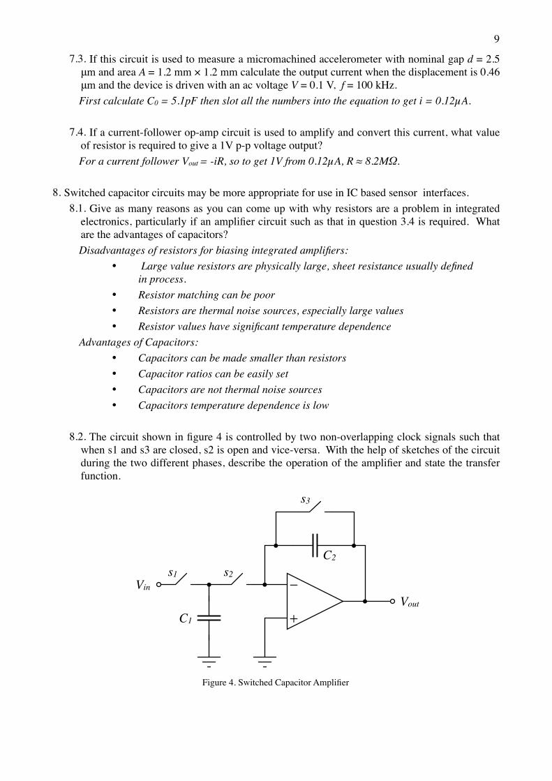
8.2. The circuit shown in figure 4 is controlled by two non-overlapping clock signals such that when s1 and s3 are closed, s2 is open and vice-versa. With the help of sketches of the circuit during the two different phases, describe the operation of the amplifier and state the transfer function.
�Figure 4. Switched Capacitor Amplifier
C1
−
+
C2
s1 s2
s3
Vin
Vout
�10
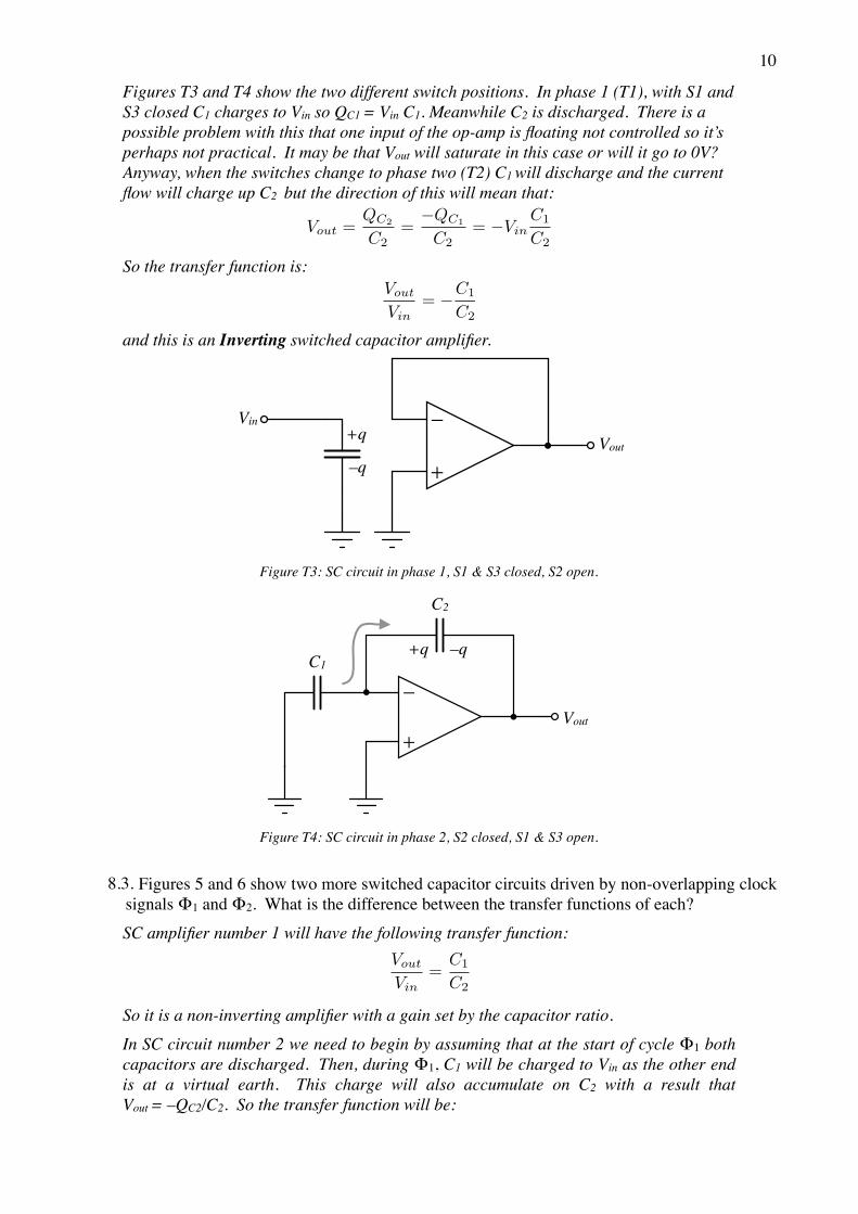
Figures T3 and T4 show the two different switch positions. In phase 1 (T1), with S1 and S3 closed C1 charges to Vin so QC1 = Vin C1. Meanwhile C2 is discharged. There is a possible problem with this that one input of the op-amp is floating not controlled so it’s perhaps not practical. It may be that Vout will saturate in this case or will it go to 0V? Anyway, when the switches change to phase two (T2) C1 will discharge and the current flow will charge up C2 but the direction of this will mean that:
�So the transfer function is:
�and this is an Inverting switched capacitor amplifier.
�Figure T3: SC circuit in phase 1, S1 & S3 closed, S2 open.
�Figure T4: SC circuit in phase 2, S2 closed, S1 & S3 open.
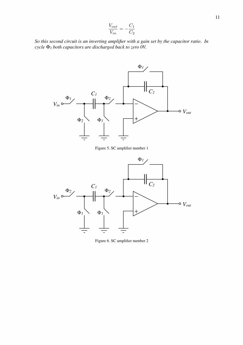
8.3. Figures 5 and 6 show two more switched capacitor circuits driven by non-overlapping clock signals Φ1 and Φ2. What is the difference between the transfer functions of each?SC amplifier number 1 will have the following transfer function:
�So it is a non-inverting amplifier with a gain set by the capacitor ratio. In SC circuit number 2 we need to begin by assuming that at the start of cycle Φ1 both capacitors are discharged. Then, during Φ1, C1 will be charged to Vin as the other end is at a virtual earth. This charge will also accumulate on C2 with a result that Vout = –QC2/C2. So the transfer function will be:
Vout
=Q
C2
C2=
�QC1
C2= �V
in
C1
C2
Vout
Vin
= �C1
C2
−
+
+q
–q
Vin
Vout
−
+
C2
C1
Vout
+q –q
Vout
Vin
=C1
C2
�11
�So this second circuit is an inverting amplifier with a gain set by the capacitor ratio. In cycle Φ2 both capacitors are discharged back to zero 0V.
�Figure 5. SC amplifier number 1
�Figure 6. SC amplifier number 2
Vout
Vin
= �C1
C2
C1 C2Φ1
Vin
Vout
−
+Φ1
Φ1
Φ2
Φ2
C1 C2Φ2
Vin
Vout
−
+Φ1
Φ1
Φ1
Φ2