Embed Size (px)
Citation preview
145
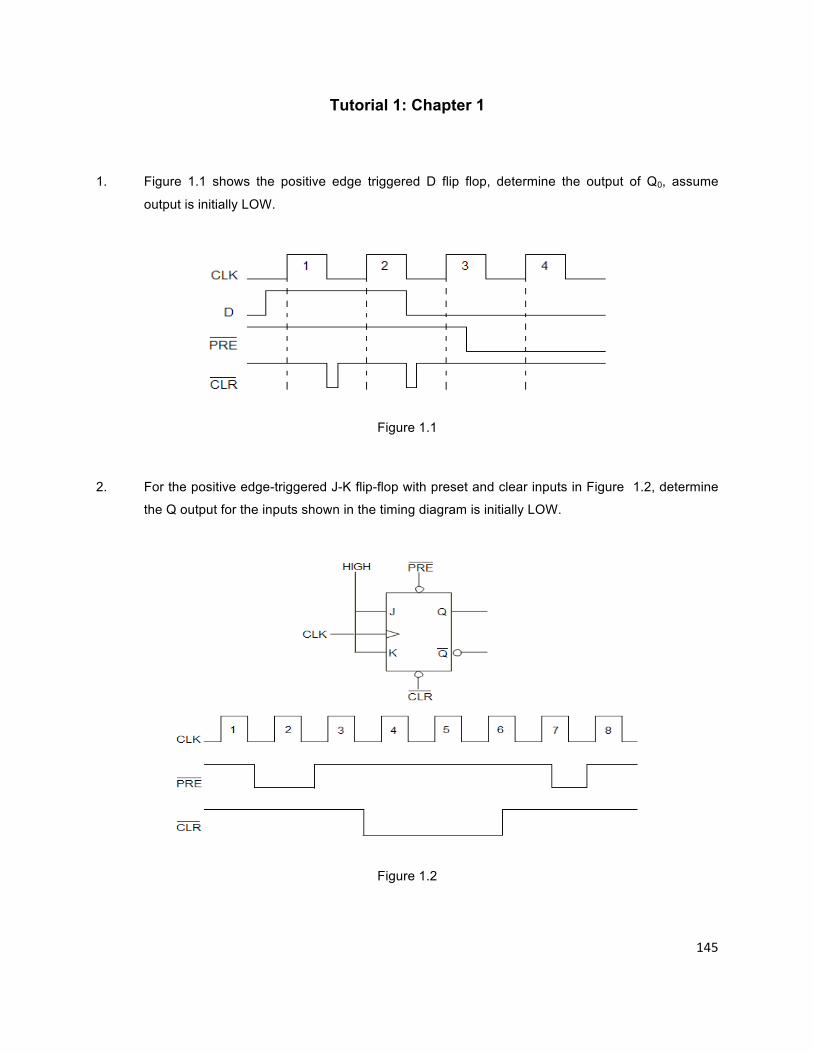
Tutorial 1: Chapter 1
1. Figure 1.1 shows the positive edge triggered D flip flop, determine the output of Q0, assume
output is initially LOW.
Figure 1.1
2. For the positive edge-triggered J-K flip-flop with preset and clear inputs in Figure 1.2, determine
the Q output for the inputs shown in the timing diagram is initially LOW.
Figure 1.2
146
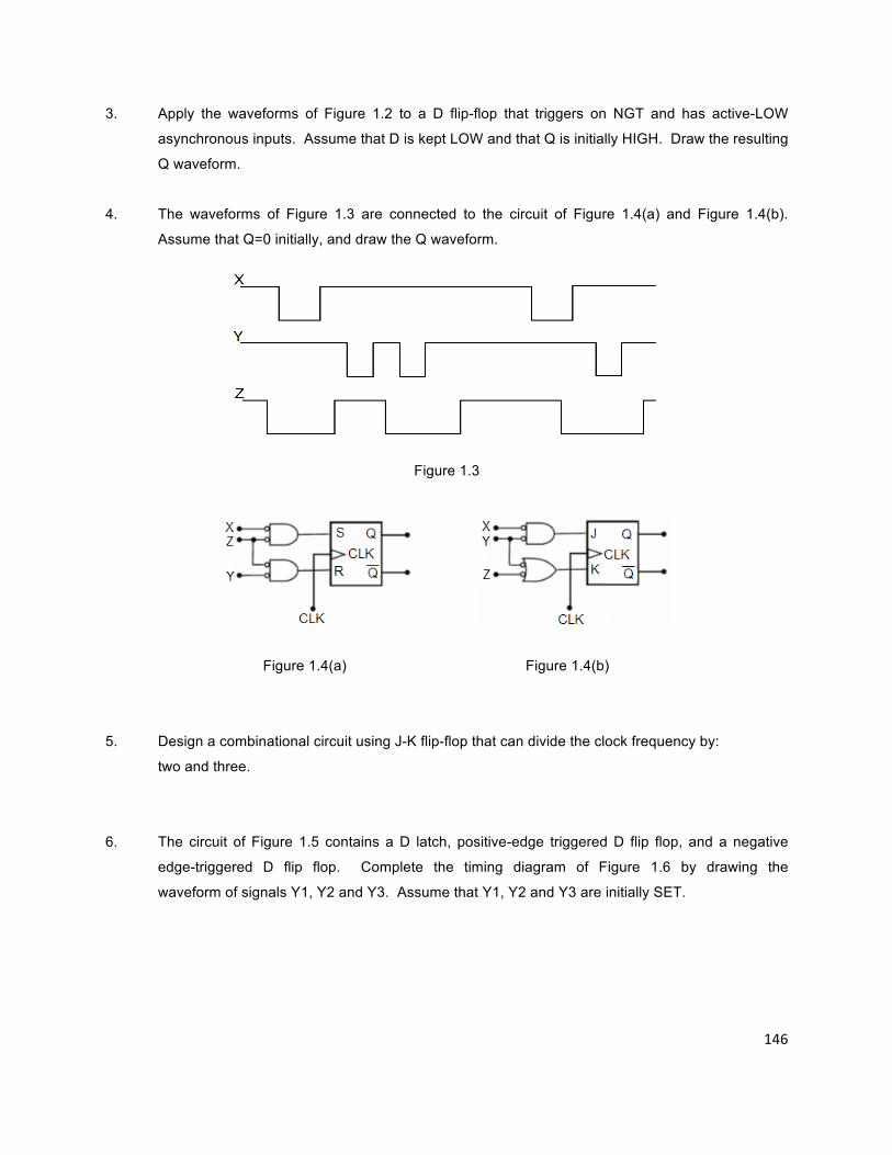
3. Apply the waveforms of Figure 1.2 to a D flip-flop that triggers on NGT and has active-LOW
asynchronous inputs. Assume that D is kept LOW and that Q is initially HIGH. Draw the resulting
Q waveform.
4. The waveforms of Figure 1.3 are connected to the circuit of Figure 1.4(a) and Figure 1.4(b).
Assume that Q=0 initially, and draw the Q waveform.
Figure 1.3
Figure 1.4(a) Figure 1.4(b)
5. Design a combinational circuit using J-K flip-flop that can divide the clock frequency by:
two and three.
6. The circuit of Figure 1.5 contains a D latch, positive-edge triggered D flip flop, and a negative
edge-triggered D flip flop. Complete the timing diagram of Figure 1.6 by drawing the
waveform of signals Y1, Y2 and Y3. Assume that Y1, Y2 and Y3 are initially SET.
147
Figure 1.5
Figure 1.6
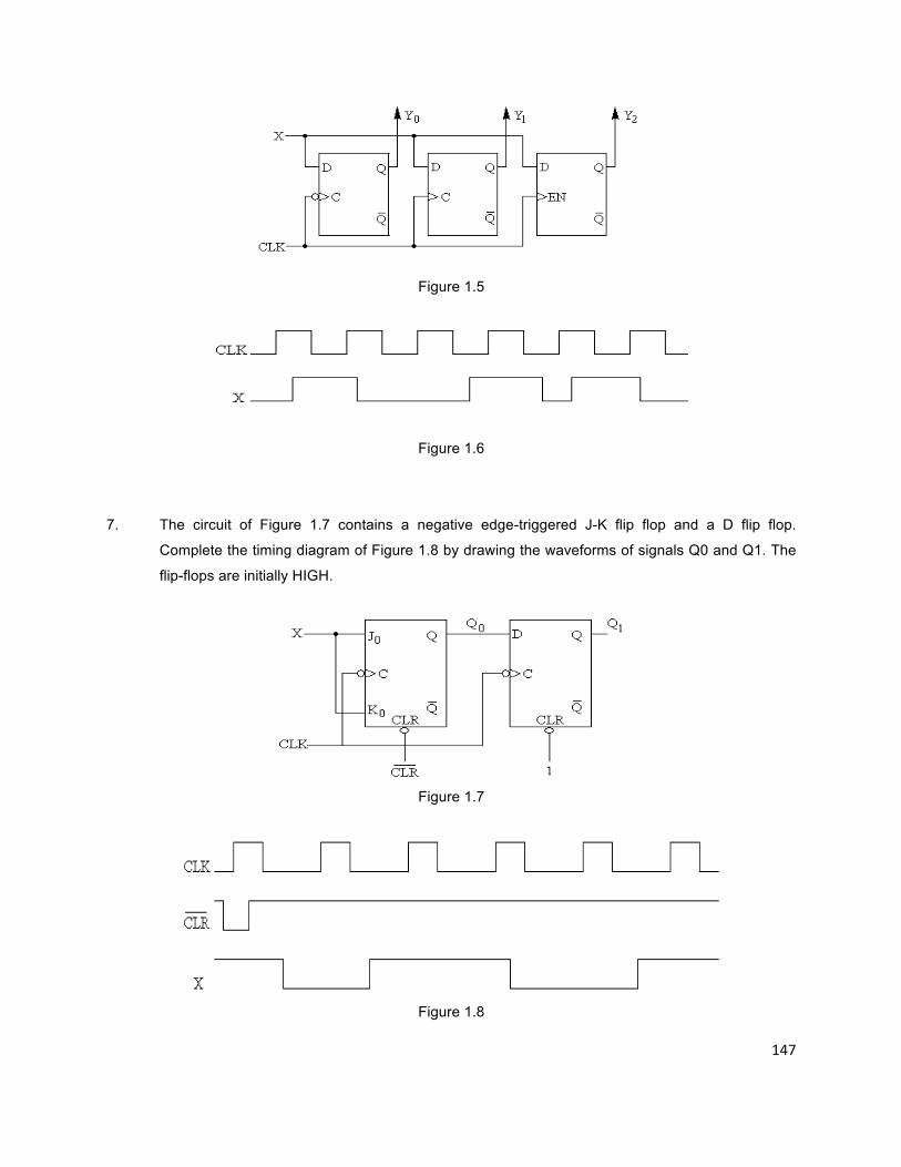
7. The circuit of Figure 1.7 contains a negative edge-triggered J-K flip flop and a D flip flop.
Complete the timing diagram of Figure 1.8 by drawing the waveforms of signals Q0 and Q1. The
flip-flops are initially HIGH.
Figure 1.7
Figure 1.8
148
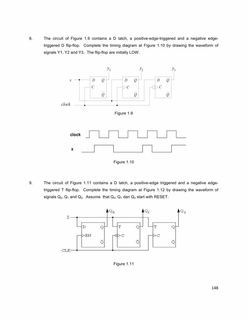
8. The circuit of Figure 1.9 contains a D latch, a positive-edge-triggered and a negative edge-
triggered D flip-flop. Complete the timing diagram at Figure 1.10 by drawing the waveform of
signals Y1, Y2 and Y3. The flip-flop are initially LOW.
Figure 1.9
Figure 1.10
9. The circuit of Figure 1.11 contains a D latch, a positive-edge triggered and a negative edge-
triggered T flip-flop. Complete the timing diagram at Figure 1.12 by drawing the waveform of
signals Q0, Q1 and Q2. Assume that Q0, Q1 dan Q2 start with RESET.
Figure 1.11
149
Figure 1.12
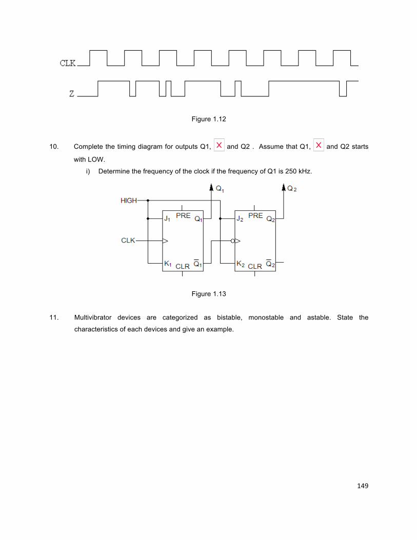
10. Complete the timing diagram for outputs Q1, and Q2 . Assume that Q1, and Q2 starts
with LOW.
i) Determine the frequency of the clock if the frequency of Q1 is 250 kHz.
Figure 1.13
11. Multivibrator devices are categorized as bistable, monostable and astable. State the
characteristics of each devices and give an example.
150
Tutorial 2: Chapter 2
1. What is does the term asynchronous mean in relation to counter?
2. What is advantage of synchronous counter over an asynchronous counter?
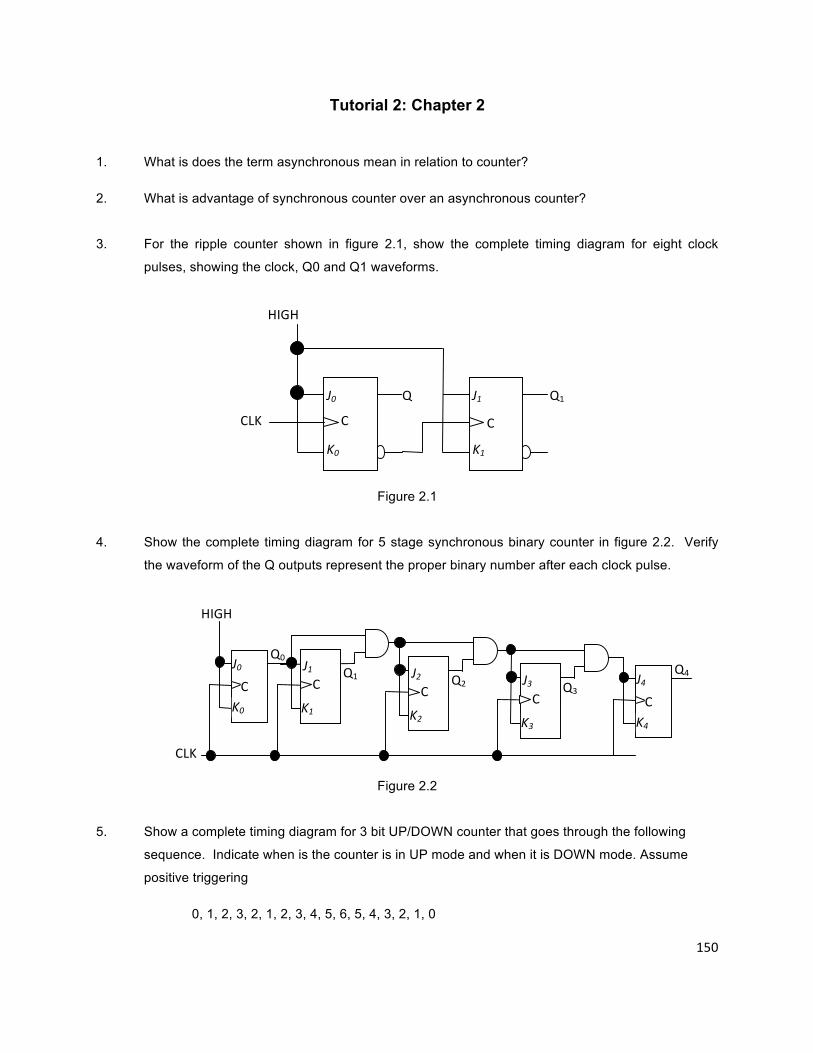
3. For the ripple counter shown in figure 2.1, show the complete timing diagram for eight clock
pulses, showing the clock, Q0 and Q1 waveforms.
Figure 2.1
4. Show the complete timing diagram for 5 stage synchronous binary counter in figure 2.2. Verify
the waveform of the Q outputs represent the proper binary number after each clock pulse.
Figure 2.2
5. Show a complete timing diagram for 3 bit UP/DOWN counter that goes through the following
sequence. Indicate when is the counter is in UP mode and when it is DOWN mode. Assume
positive triggering
0, 1, 2, 3, 2, 1, 2, 3, 4, 5, 6, 5, 4, 3, 2, 1, 0
HIGH
CLK
Q0
K0
J0
C Q1
J1
K1
C Q3 J3
K3
C Q2
J2
K2
C
Q4
K4
J4
C
J0
K0
J1
K1
C C CLK
Q
0 Q1
HIGH
151
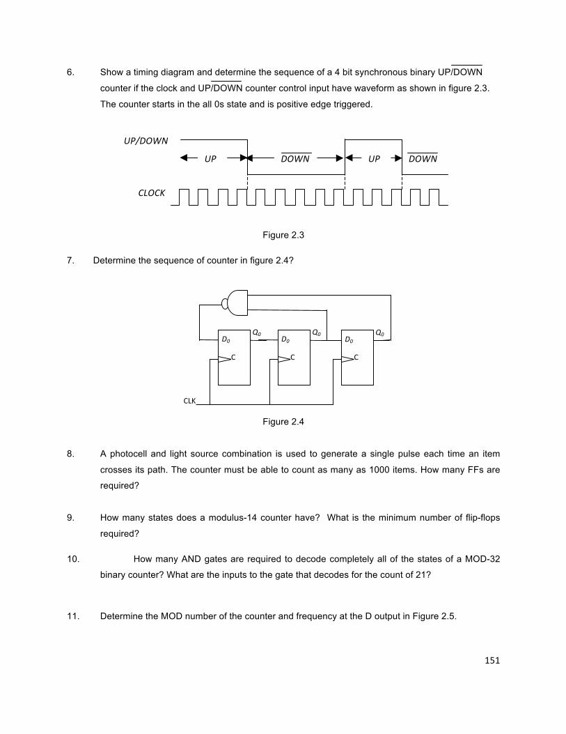
6. Show a timing diagram and determine the sequence of a 4 bit synchronous binary UP/DOWN
counter if the clock and UP/DOWN counter control input have waveform as shown in figure 2.3.
The counter starts in the all 0s state and is positive edge triggered.
Figure 2.3
7. Determine the sequence of counter in figure 2.4?
Figure 2.4
8. A photocell and light source combination is used to generate a single pulse each time an item
crosses its path. The counter must be able to count as many as 1000 items. How many FFs are
required?
9. How many states does a modulus-14 counter have? What is the minimum number of flip-flops
required?
10. How many AND gates are required to decode completely all of the states of a MOD-32
binary counter? What are the inputs to the gate that decodes for the count of 21?
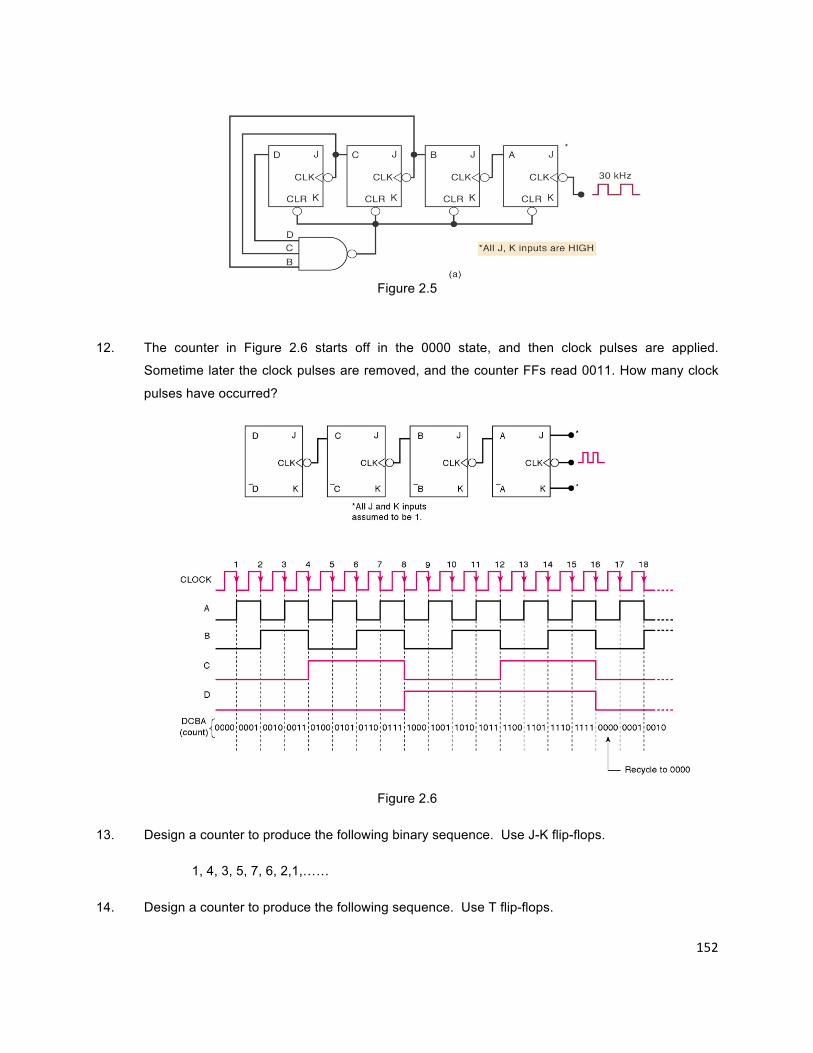
11. Determine the MOD number of the counter and frequency at the D output in Figure 2.5.
DOWN
UP/DOWN
DOWN UP UP
CLOCK
D0
C
Q0
CLK
D0
C
Q0 D0
C
Q0
152
Figure 2.5
12. The counter in Figure 2.6 starts off in the 0000 state, and then clock pulses are applied.
Sometime later the clock pulses are removed, and the counter FFs read 0011. How many clock
pulses have occurred?
Figure 2.6
13. Design a counter to produce the following binary sequence. Use J-K flip-flops.
1, 4, 3, 5, 7, 6, 2,1,……
14. Design a counter to produce the following sequence. Use T flip-flops.
153
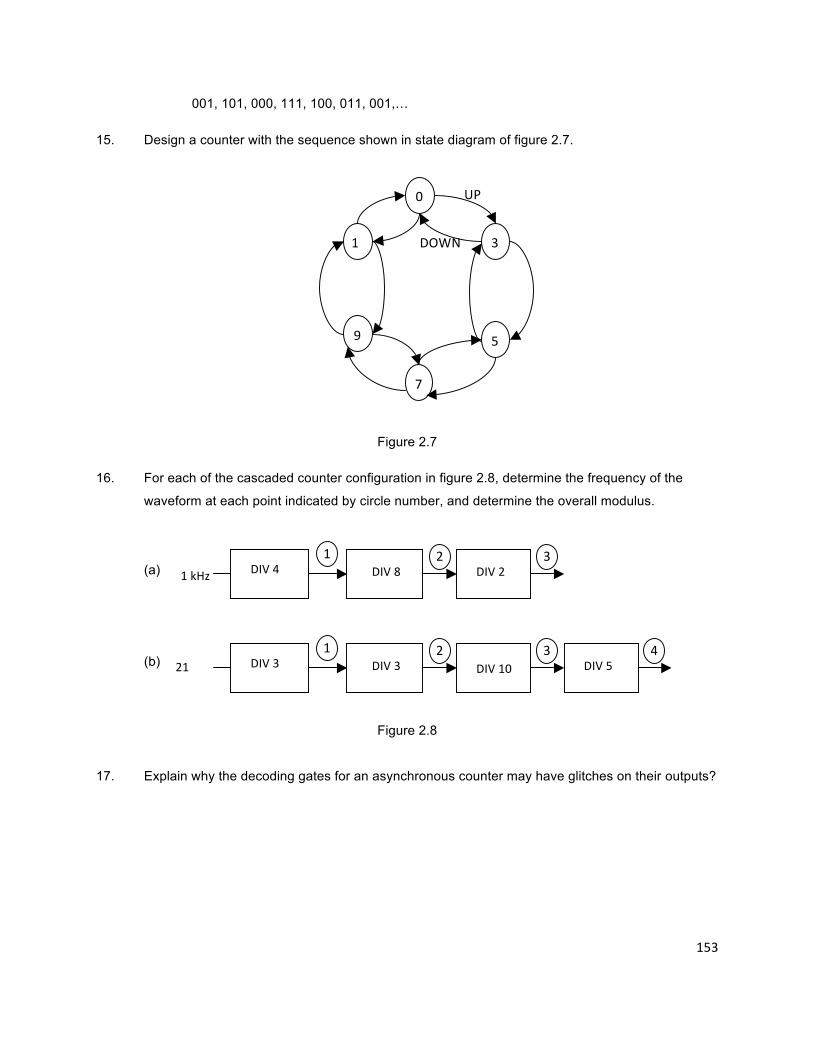
001, 101, 000, 111, 100, 011, 001,…
15. Design a counter with the sequence shown in state diagram of figure 2.7.
Figure 2.7
16. For each of the cascaded counter configuration in figure 2.8, determine the frequency of the
waveform at each point indicated by circle number, and determine the overall modulus.
(a)
(b)
Figure 2.8
17. Explain why the decoding gates for an asynchronous counter may have glitches on their outputs?
UP
DOWN
0
0
7
30
5
0
111
0
9
1 2 3 DIV 4
IV 8
DIV 8 DIV 2 1 kHz
4 DIV 5 DIV 3
IV 8
21
kHz
1 DIV 3
2 3 DIV 10
154
Tutorial 3: Chapter 3
1. Mrs. Brooke owns a robot with an FSM brain. The robot walks from left to right along a paper type
containing a sequence of 1’s and 0’s. On each clock cycle, the robot walks to the next bit. An
indicator on the robot’s body will light up when the last four bits that it has walked over are, from
left to right, 1101. Design the FSM to compute when the robot should indicate a light. The input A
is the bit underneath the robot’s legs. The output Y is TRUE when the indicator lights up.
a. Sketch a timing diagram for each machine showing the input, states and output
as your robot walks along the sequence 111011010.
b. Compare Moore and Mealy state machine designs.
c. Simulate your design in Multisim using T flip-flop.
2. A sequential system is the controller for a stamp-vending machine. There is an input to reset the
controller (put in the initial state), one input whose value corresponds to the type of coin inserted
either 10¢ or 20¢ (Malaysia’s currency coins), one input to select between three choices of
stamps and one input to request return of coins. Assume that the values of three selections are
20 cents, 40 cents and 50 cents and that the machine should give change. The outputs are
release stamp 1, release stamp 2, release stamp 3, return coin give 10 cents change.
a. Design a Moore machine using D flip-flop
b. Simulate your design in Multisim.
3. A sequential network has one input (X) and two outputs (Z1 and Z2). An output Z1=1 occurs every
time the input sequence 010 is completed provided that the sequence 100 has never occurred.
An output Z2=1 occurs every time the input sequence 100 is completed. Note that once a Z2=1
output has occurred, Z1= 1 can never occur, but not vice versa [3].
a. Derive a Mealy state diagram.
b. Realize the network using T flip-flops and NAND gates. Repeat using NOR gates. (Work
this part by hand)
c. Simulate your design in b) using Multisim.
4. Ben decides to solve the problem with an FSM. He installs two traffic sensors, TA and TB on
Academic Ave and Bravado Blvd respectively. Each sensor indicates TRUE if students are
present and FALSE if the street is empty. He also installs two traffic lights, LA and LB to control
traffic. Each light receives digital inputs specifying whether it should be green, yellow or red.
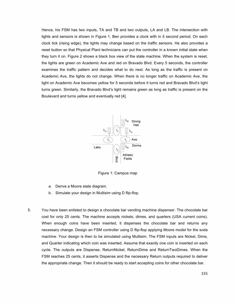
155
Hence, his FSM has two inputs, TA and TB and two outputs, LA and LB. The intersection with
lights and sensors is shown in Figure 1. Ben provides a clock with in 5 second period. On each
clock tick (rising edge), the lights may change based on the traffic sensors. He also provides a
reset button so that Physical Plant technicians can put the controller in a known initial state when
they turn it on. Figure 2 shows a black box view of the state machine. When the system is reset,
the lights are green on Academic Ave and red on Bravado Blvd. Every 5 seconds, the controller
examines the traffic pattern and decides what to do next. As long as the traffic is present on
Academic Ave, the lights do not change. When there is no longer traffic on Academic Ave, the
light on Academic Ave becomes yellow for 5 seconds before it turns red and Bravado Blvd’s light
turns green. Similarly, the Bravado Blvd’s light remains green as long as traffic is present on the
Boulevard and turns yellow and eventually red [4].
Figure 1: Campus map
a. Derive a Moore state diagram.
b. Simulate your design in Multisim using D flip-flop.
5. You have been enlisted to design a chocolate bar vending machine dispenser. The chocolate bar
cost for only 25 cents. The machine accepts nickels, dimes, and quarters (USA current coins).
When enough coins have been inserted, it dispenses the chocolate bar and returns any
necessary change. Design an FSM controller using D flip-flop applying Moore model for the soda
machine. Your design is then to be simulated using Multisim. The FSM inputs are Nickel, Dime,
and Quarter indicating which coin was inserted. Assume that exactly one coin is inserted on each
cycle. The outputs are Dispense, ReturnNickel, ReturnDime and ReturnTwoDimes. When the
FSM reaches 25 cents, it asserts Dispense and the necessary Return outputs required to deliver
the appropriate change. Then it should be ready to start accepting coins for other chocolate bar.
156
Tutorial 4: Chapter 4
1. How many clock pulse are needed to get the complete data for the following shift registers:
a. 5-bit serial to parallel shift register
b. 4-bit parallel to serial shift register
2. Determine the output of serial to parallel register for the following conditions:
a. after three clock pulses initially loaded with 101011
b. after four clock pulses initially loaded with 000111011
3. Determine the output of parallel to serial register for the following condition:
a. after two clock pulses initially loaded with 11011
b. after five clock pulses initially loaded with 00101
4. What two principal functions are performed by a shift register?
5. How many clock pulses are required to enter a byte of data serially into an 8-bit shift register?
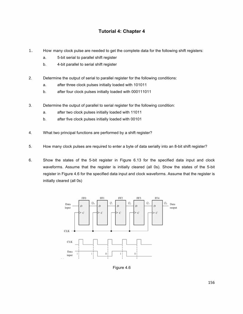
6. Show the states of the 5-bit register in Figure 6.13 for the specified data input and clock
waveforms. Assume that the register is initially cleared (all 0s). Show the states of the 5-bit
register in Figure 4.6 for the specified data input and clock waveforms. Assume that the register is
initially cleared (all 0s)
Figure 4.6
157
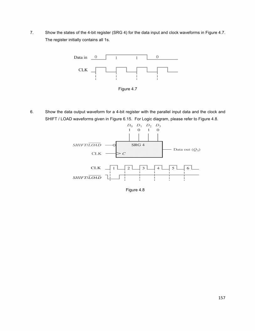
7. Show the states of the 4-bit register (SRG 4) for the data input and clock waveforms in Figure 4.7.
The register initially contains all 1s.
Figure 4.7
6. Show the data output waveform for a 4-bit register with the parallel input data and the clock and
SHIFT / LOAD waveforms given in Figure 6.15. For Logic diagram, please refer to Figure 4.8.
Figure 4.8
158
Tutorial 5: Chapter 5
1. What is the smallest unit of data that can be stored in a memory?
2. What is the bit capacity of a memory that can store 256 bytes of data?
3. What is a read and write operation in memory?
4. Explain how SRAMs and DRAMs differ?
5. List four types of DRAM?
6. What is the bit storage capacity of a ROM with a 512 X 8 organization?
7. How many address bits are required for a 2048-bit memory organized as a 256 X 8 memory?
8. How do PROMs differ from ROMs?
9. How many 16k x 1 RAMs are required to achieve a memory with a word capacity of 16k and a
word length of eight bits?
10. What is FIFO and LIFO memory?
11. What is difference between GAL and PAL?
12. What does a macrocell contain?
13. What is a CPLD?
14. Explain the purpose of the XOR gate in the macrocell.
15. What are the two major modes of a macrocell?
16. Besides the OR gate, XOR gate, and flip-flop, what other logic element is commonly used in a
macrocell?
159
17. How does FPGA differ from CPLD?
18. Describe an LUT and discuss its purpose
19. What does CLB in a Xilinx FPGA consist of?
20. Describe a slice in a Xilinx FPGA.