Embed Size (px)
Citation preview
S. Yuasa, R. Matsumoto, A. Fukushima, H. Kubota, K. Yakushiji, T. Nakamura,
Y. Suzuki and K. Ando
Tunnel Magnetoresistance Effect and Its Applications
Collaborators
Canon Anelva Corp. (R & D of manufacturing technology)
Toshiba Corp.(R & D of Spin-MRAM)
Funding agencies
Osaka University (High-frequency experiment)
(1) Introduction
(2) Epitaxial MTJs with a crystalline MgO(001) barrier
(3) CoFeB / MgO / CoFeB MTJs for device applications
Outline
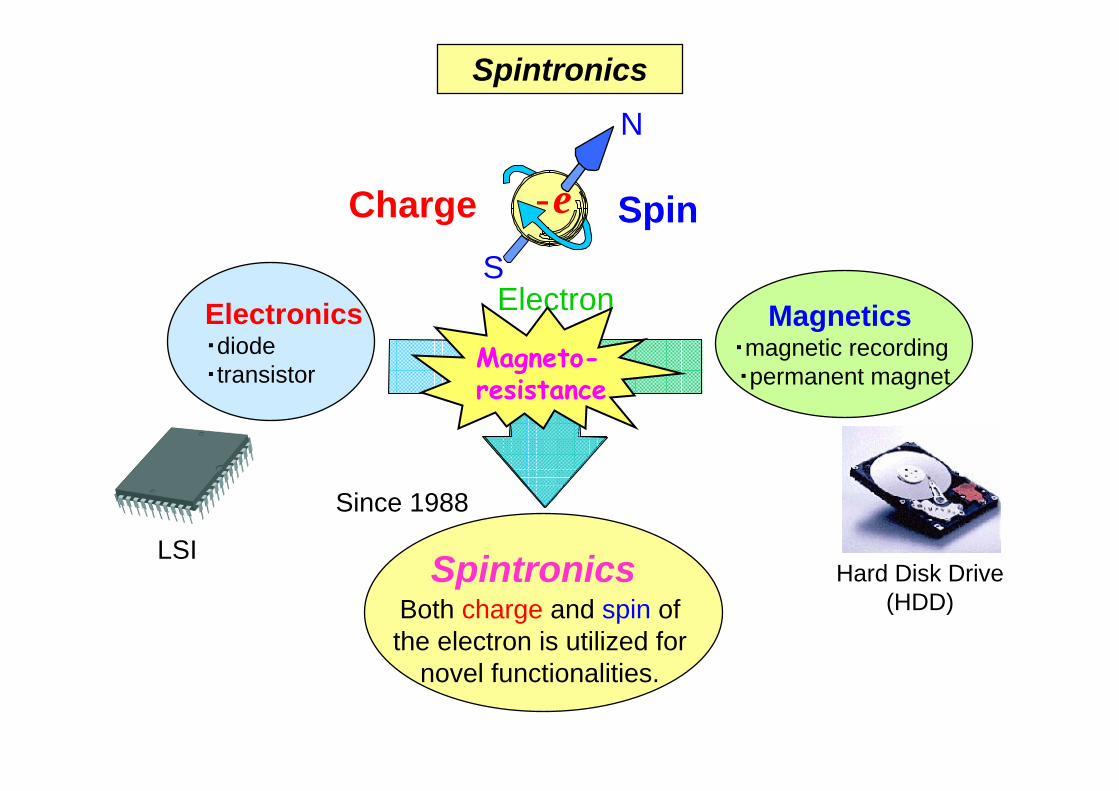
Electronics・diode ・transistor
LSI
Magnetics・magnetic recording ・permanent magnet
Hard Disk Drive(HDD)
SpintronicsBoth charge and spin of the electron is utilized for
novel functionalities.
Since 1988
Electron
Charge -e Spin
N
S
Spintronics
Magneto-resistance
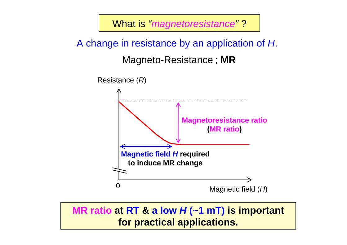
What is “magnetoresistance” ?
A change in resistance by an application of H.
Magneto-Resistance ; MR
Resistance (R)
Magnetic field (H) 0
Magnetic field H required to induce MR change
Magnetoresistance ratio(MR ratio)
MR ratio at RT & a low H (~1 mT) is important for practical applications.
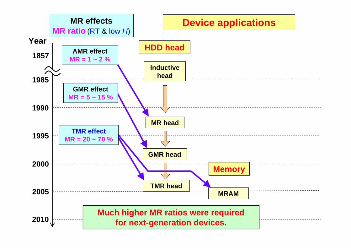
Year
1995
2000
2005
2010
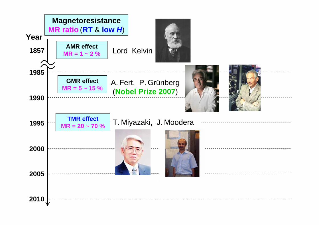
MagnetoresistanceMR ratio (RT & low H)
1857
1985
1990
AMR effect MR = 1 ~ 2 % Lord Kelvin
GMR effectMR = 5 ~ 15 %
A. Fert, P. Grünberg(Nobel Prize 2007)
T. Miyazaki, J. Moodera TMR effectMR = 20 ~ 70 %
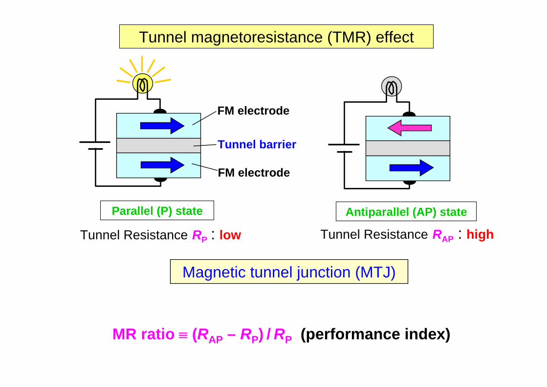
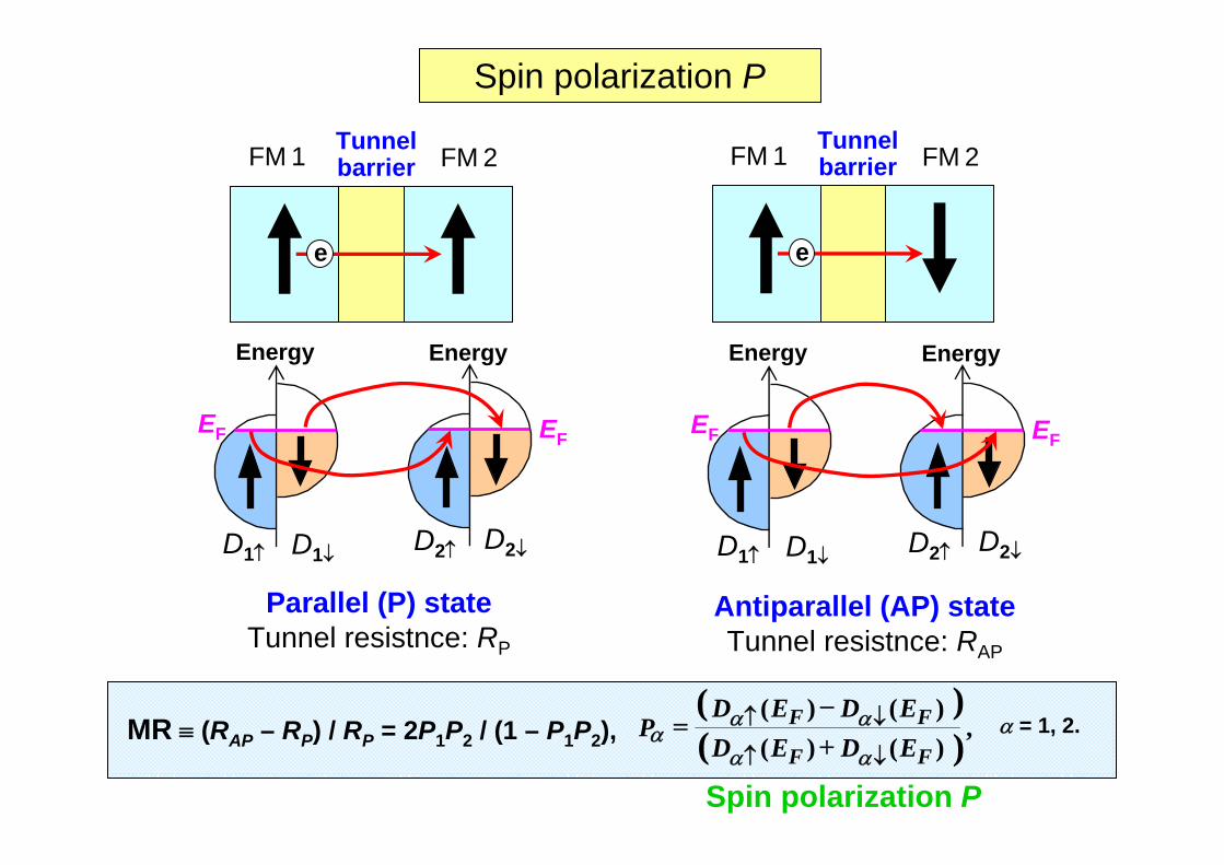
Tunnel magnetoresistance (TMR) effect
Tunnel barrier
FM electrode
FM electrode
Tunnel Resistance RP : low
Parallel (P) state
Tunnel Resistance RAP : high
Antiparallel (AP) state
Magnetic tunnel junction (MTJ)
MR ratio ≡ (RAP – RP) / RP (performance index)
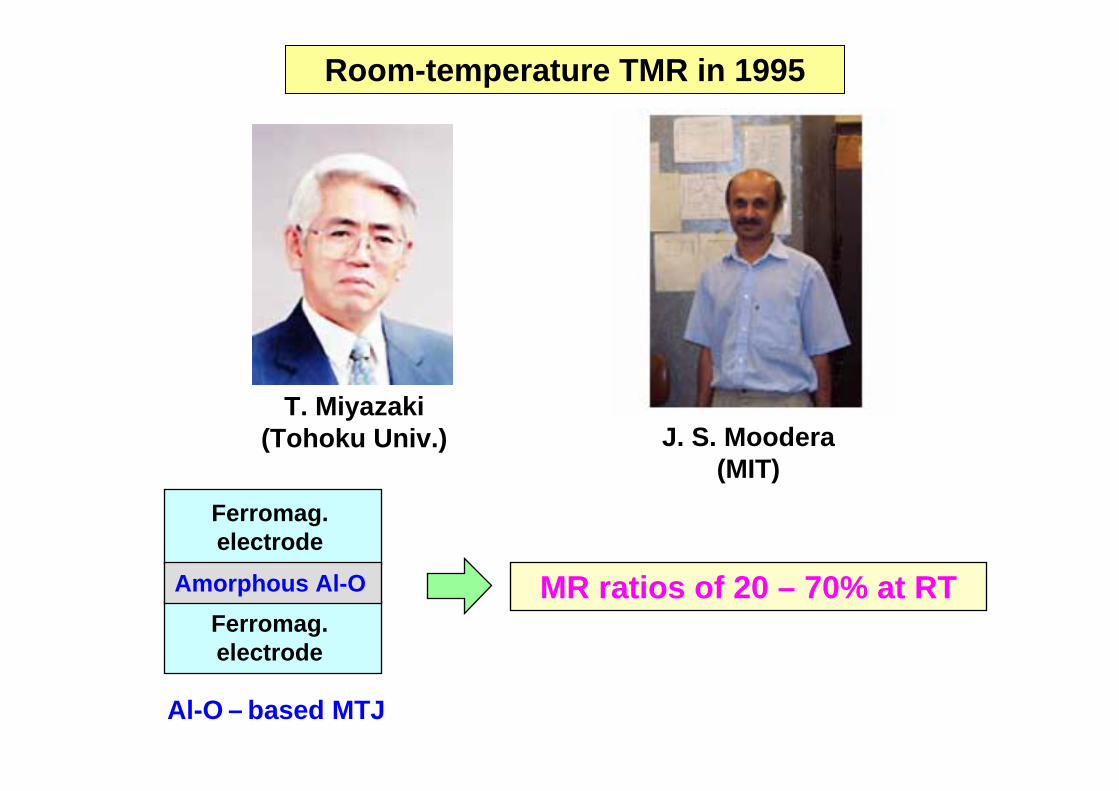
Room-temperature TMR in 1995
MR ratios of 20 – 70% at RT
T. Miyazaki (Tohoku Univ.) J. S. Moodera
(MIT) Ferromag. electrode
Ferromag. electrode
Amorphous Al-O
Al-O – based MTJ
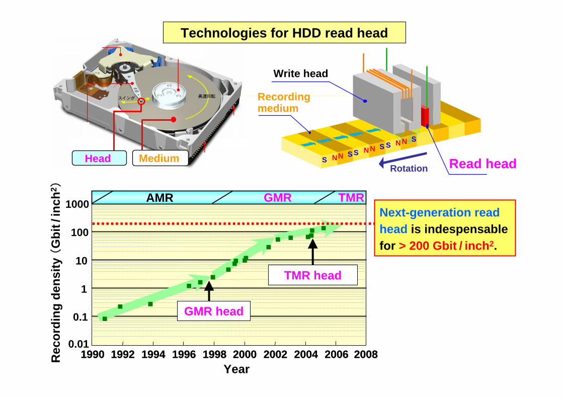
GMRヘッドの出現
0.01
0.1
1
10
100
1000
■■
■
■
■ ■
■■
■
■■■
■■
■■
■
■
■
■ ■
■■
■
■■■
■■
AMR GMR TMR
■■
1990 1992 1994 1996 1998 2000 2002 2004 2006 20081990 1992 1994 1996 1998 2000 2002 2004 2006 2008Year
GMR head
■
TMR head
■■■
Rec
ordi
ng d
ensi
ty (
Gbi
t/in
ch2 )
Recording medium
N SS N
N SS N
N SS N
Rotation
N SS N
N SS N
N SS N Read head
Write head
Next-generation read head is indespensablefor > 200 Gbit / inch2.
Head Medium
Technologies for HDD read head
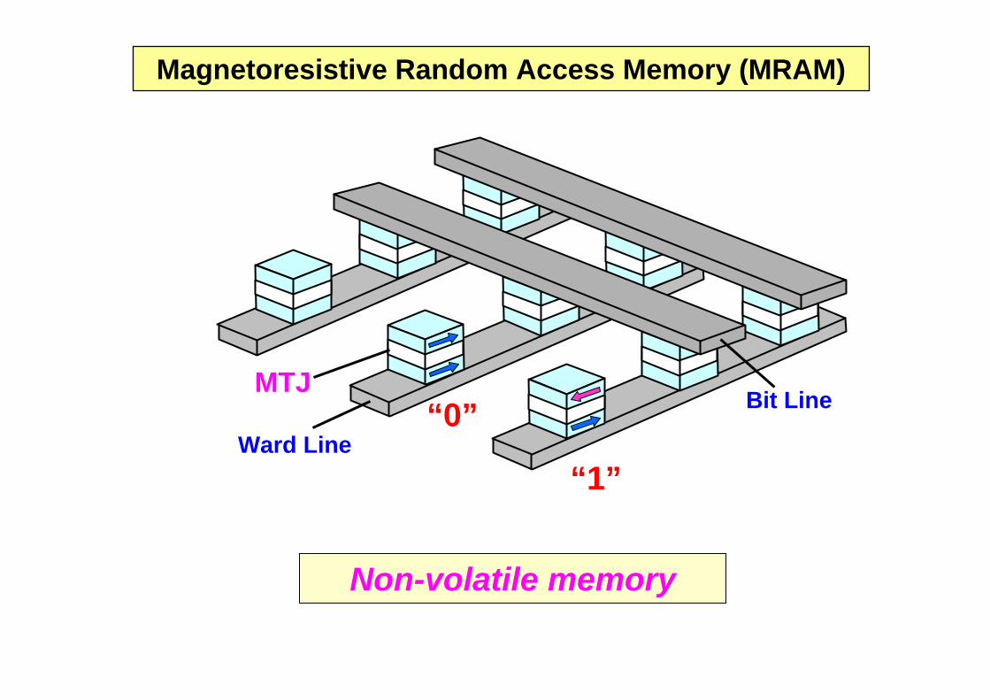
Ward Line
Bit Line MTJ
“1”
“0”
Non-volatile memory
Magnetoresistive Random Access Memory (MRAM)
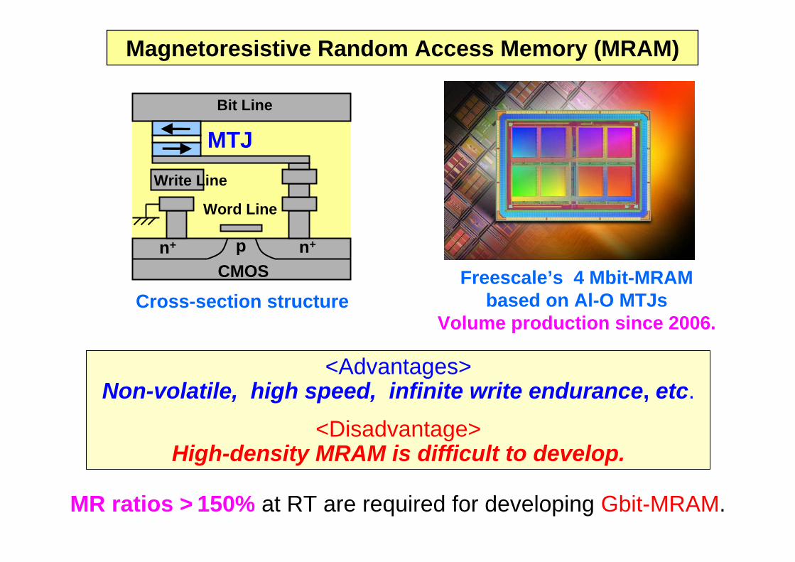
Freescale’s 4 Mbit-MRAM based on Al-O MTJs
Volume production since 2006.
Magnetoresistive Random Access Memory (MRAM)
CMOS
MTJBit Line
Write Line
n+ p n+
Word Line
Cross-section structure
<Advantages> Non-volatile, high speed, infinite write endurance, etc.
<Disadvantage>High-density MRAM is difficult to develop.
MR ratios > 150% at RT are required for developing Gbit-MRAM.
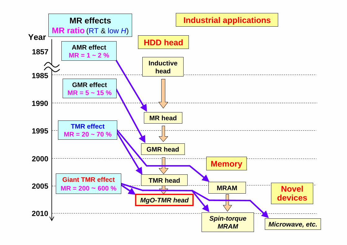
Year
1995
2000
2005
2010
1857
1985
1990
MR effects MR ratio (RT & low H)
Device applications
MR head
GMR head
TMR head
HDD head
Inductivehead
MRAM
Memory
Much higher MR ratios were required for next-generation devices.
AMR effect MR = 1 ~ 2 %
TMR effectMR = 20 ~ 70 %
GMR effectMR = 5 ~ 15 %
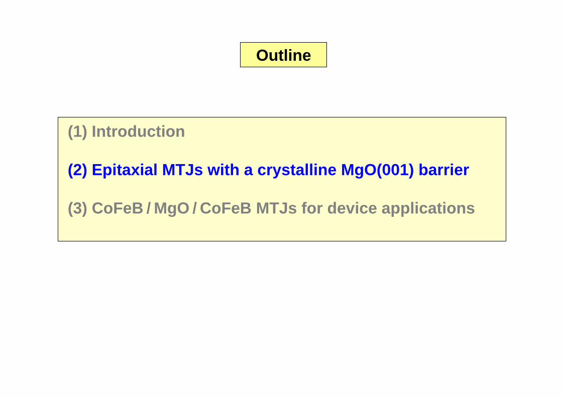
(1) Introduction
(2) Epitaxial MTJs with a crystalline MgO(001) barrier
(3) CoFeB / MgO / CoFeB MTJs for device applications
Outline
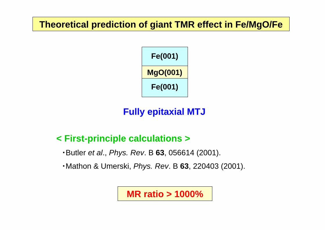
Theoretical prediction of giant TMR effect in Fe/MgO/Fe
・Butler et al., Phys. Rev. B 63, 056614 (2001).
・Mathon & Umerski, Phys. Rev. B 63, 220403 (2001).
< First-principle calculations >
MR ratio > 1000%
Fully epitaxial MTJ
Fe(001)
Fe(001)
MgO(001)
Tunnel barrier FM 1
e
FM 2
Parallel (P) stateTunnel resistnce: RP
D1↑ D1↓
Energy
D2↑ D2↓
EF EF
Spin polarization P
MR ≡ (RAP – RP) / RP = 2P1P2 / (1 – P1P2), ( )( ),
)()()()(
FF
FFEDEDEDED
P↓↑
↓↑+−
=αα
ααα α = 1, 2.
Spin polarization P
Tunnel barrier FM 1
e
FM 2
Energy
D1↑ D1↓
Energy
D2↑ D2↓
EF EF
Energy
Antiparallel (AP) stateTunnel resistnce: RAP
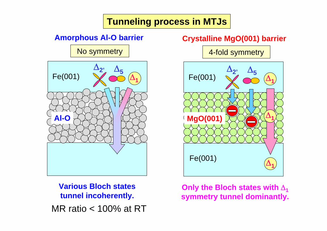
Tunneling process in MTJsAmorphous Al-O barrier
No symmetry
Various Bloch states tunnel incoherently.
Crystalline MgO(001) barrier
4-fold symmetry
MgO(001)
Fe(001)
Fe(001)
Δ2’ Δ5Δ1
Δ1
Δ1
Fe(001)
Al-O
Δ2’ Δ5Δ1
MR ratio < 100% at RT
Only the Bloch states with Δ1symmetry tunnel dominantly.
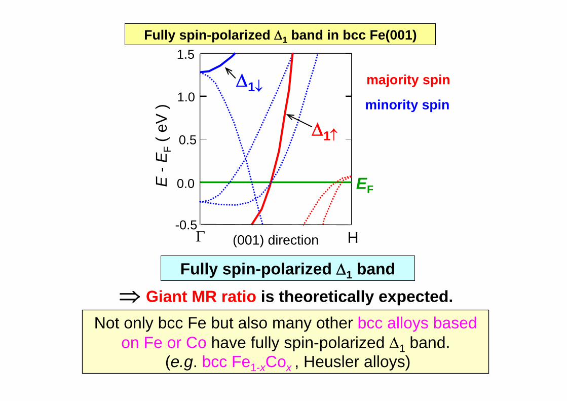
Fully spin-polarized Δ1 band in bcc Fe(001)
Fully spin-polarized Δ1 band⇒ Giant MR ratio is theoretically expected.
Not only bcc Fe but also many other bcc alloys based on Fe or Co have fully spin-polarized Δ1 band.
(e.g. bcc Fe1-xCox , Heusler alloys)
minority spin
majority spinΔ1↓
1.5
1.0
0.5
0.0
-0.5
E-E
F( e
V)
Γ H
Δ1↑
(001) direction
EF
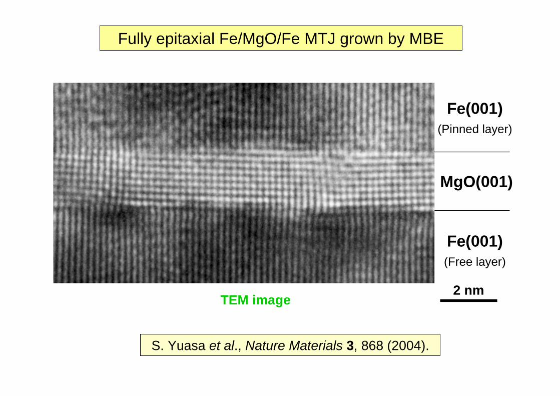
Fully epitaxial Fe/MgO/Fe MTJ grown by MBE
Fe(001)(Pinned layer)
MgO(001)
Fe(001)(Free layer)
TEM image2 nm
S. Yuasa et al., Nature Materials 3, 868 (2004).
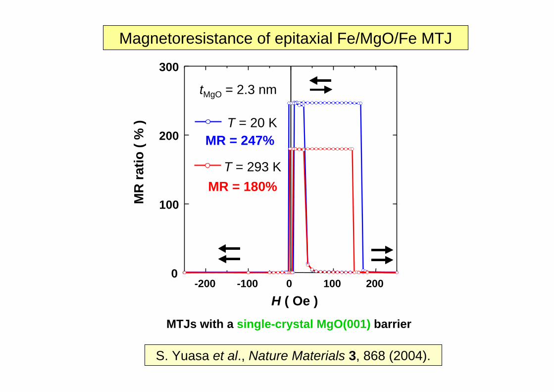
Magnetoresistance of epitaxial Fe/MgO/Fe MTJ
S. Yuasa et al., Nature Materials 3, 868 (2004).
MR = 247%
MR = 180%
-200 -100 0 100 2000
100
200
300
tMgO = 2.3 nm
T = 20 K
T = 293 K
MR
ratio
( %
)
H ( Oe )MTJs with a single-crystal MgO(001) barrier
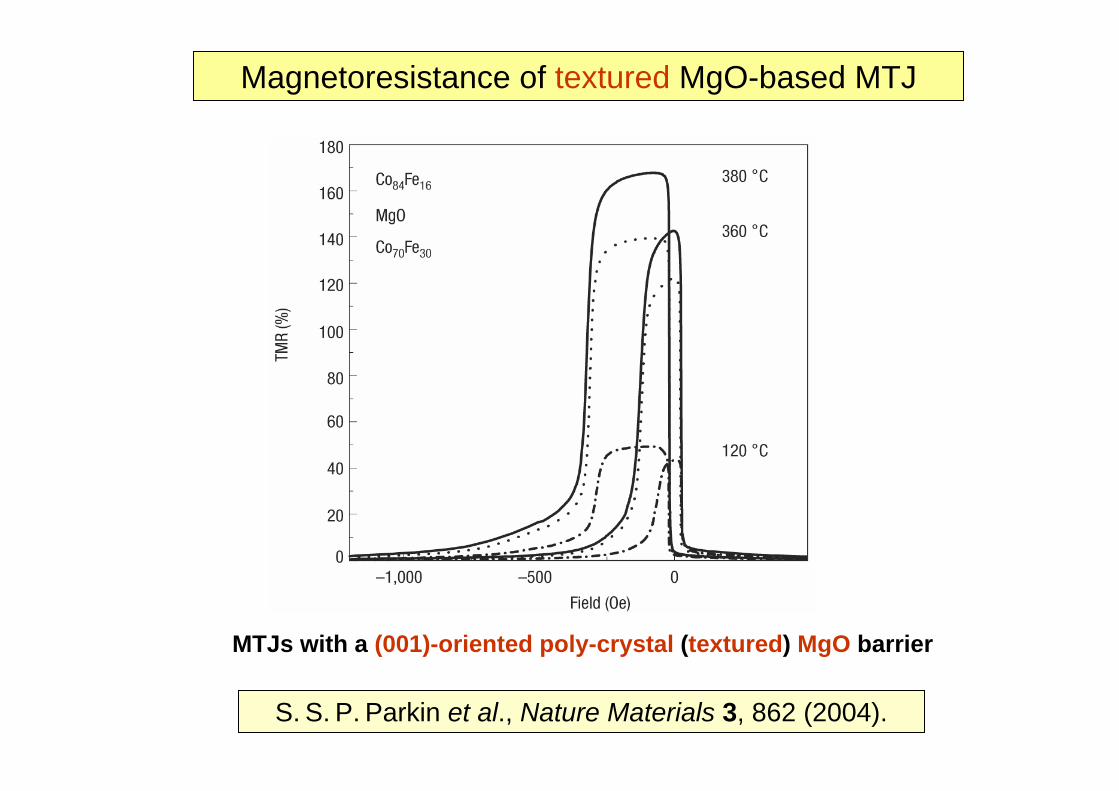
Magnetoresistance of textured MgO-based MTJ
S. S. P. Parkin et al., Nature Materials 3, 862 (2004).
MTJs with a (001)-oriented poly-crystal (textured) MgO barrier
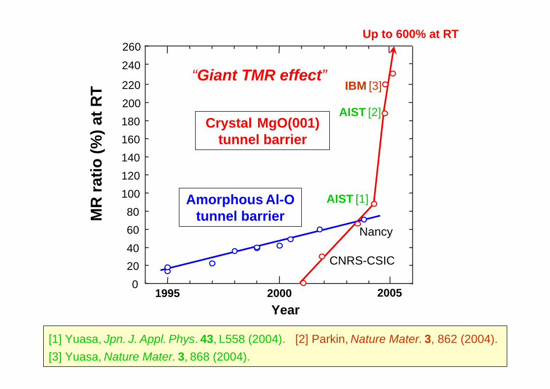
1995 20000
20406080
100120140160180200
MR
ratio
(%) a
t RT
Year
220
240
2005
260
Nancy
CNRS-CSIC
AIST [1]
AIST [2]
IBM [3]
Amorphous Al-O tunnel barrier
Crystal MgO(001) tunnel barrier
[1] Yuasa, Jpn. J. Appl. Phys. 43, L558 (2004). [2] Parkin, Nature Mater. 3, 862 (2004).[3] Yuasa, Nature Mater. 3, 868 (2004).
Up to 600% at RT
“Giant TMR effect”
(1) Introduction
(2) Epitaxial MTJs with a crystalline MgO(001) barrier
(3) CoFeB / MgO / CoFeB MTJs for device applications
Outline
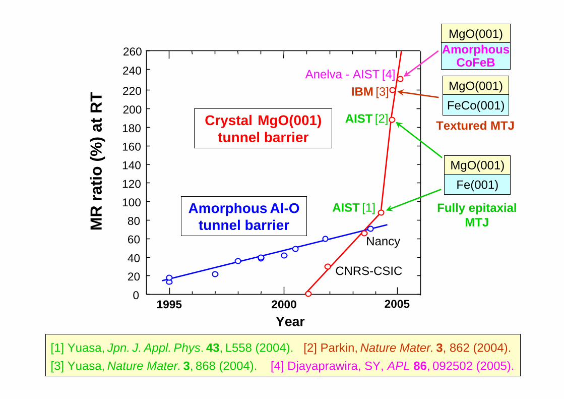
1995 20000
20406080
100120140160180200
MR
ratio
(%) a
t RT
Year
220
240
2005
260
Nancy
CNRS-CSIC
AIST [1]
AIST [2]
IBM [3]Anelva - AIST [4]
Fe(001)MgO(001)
Fully epitaxialMTJ
Textured MTJFeCo(001)MgO(001)
[1] Yuasa, Jpn. J. Appl. Phys. 43, L558 (2004). [2] Parkin, Nature Mater. 3, 862 (2004).[3] Yuasa, Nature Mater. 3, 868 (2004). [4] Djayaprawira, SY, APL 86, 092502 (2005).
Amorphous Al-O tunnel barrier
Crystal MgO(001) tunnel barrier
AmorphousCoFeB
MgO(001)
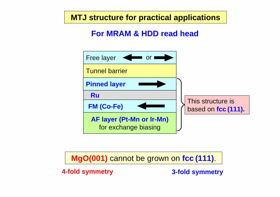
MTJ structure for practical applications
Ru
Tunnel barrier
Free layer
Pinned layer
FM (Co-Fe)
AF layer (Pt-Mn or Ir-Mn)for exchange biasing
For MRAM & HDD read head
This structure is based on fcc (111).
MgO(001) cannot be grown on fcc (111).4-fold symmetry 3-fold symmetry
or
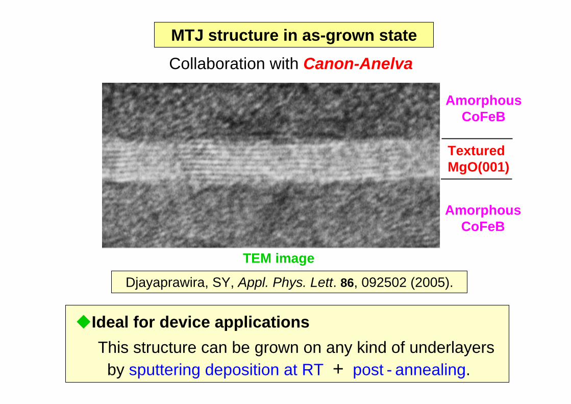
MTJ structure in as-grown state
◆Ideal for device applicationsThis structure can be grown on any kind of underlayers
by sputtering deposition at RT + post - annealing.
TexturedMgO(001)
AmorphousCoFeB
AmorphousCoFeB
Djayaprawira, SY, Appl. Phys. Lett. 86, 092502 (2005).
TEM image
Collaboration with Canon-Anelva
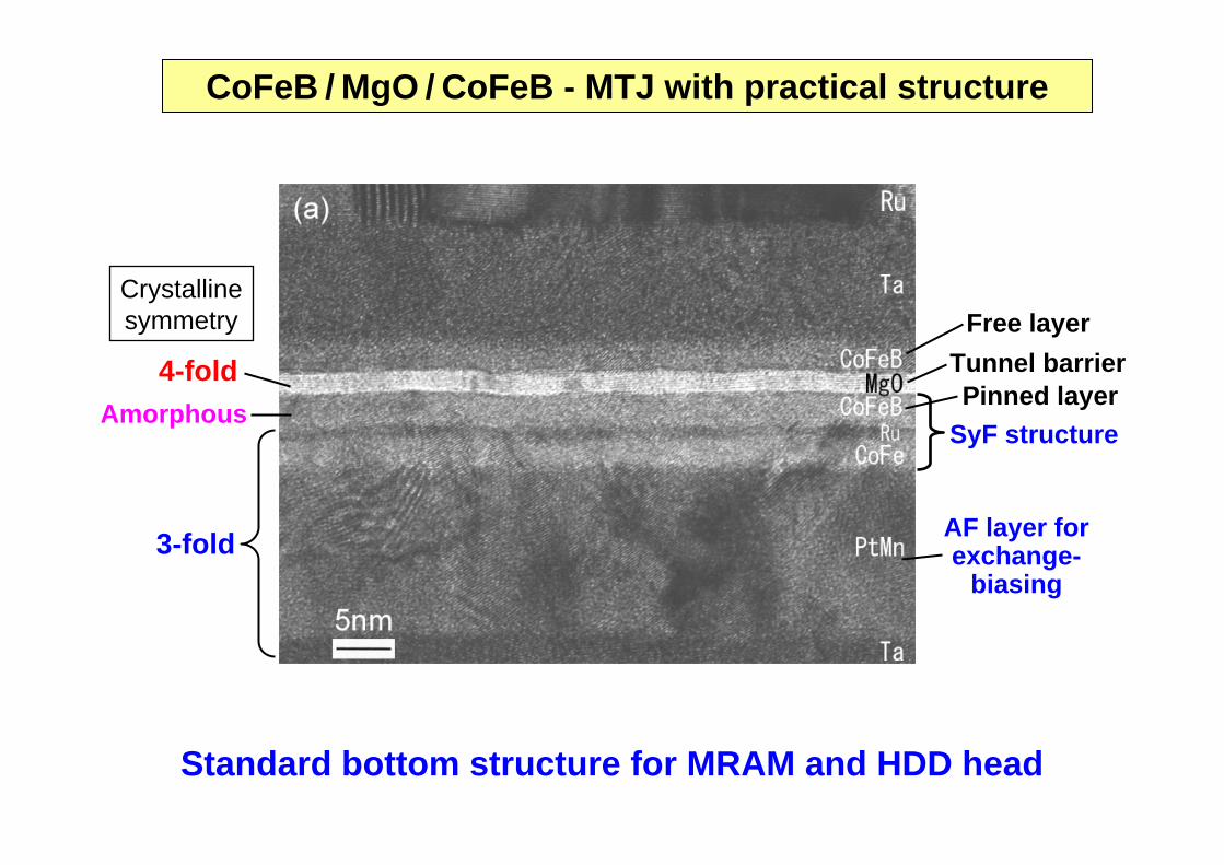
CoFeB / MgO / CoFeB - MTJ with practical structure
Standard bottom structure for MRAM and HDD head
3-fold
4-foldAmorphous
Free layerTunnel barrier
SyF structure
AF layer forexchange-
biasing
Pinned layer
Crystallinesymmetry
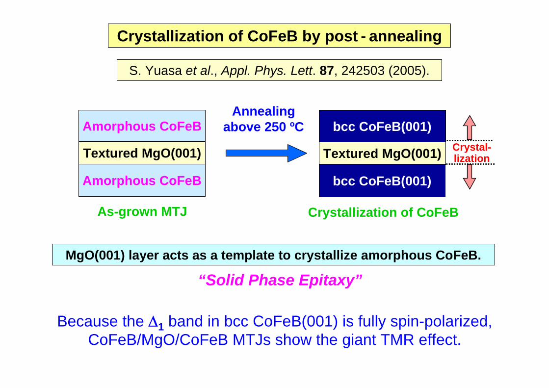
Amorphous CoFeB
Textured MgO(001)
Amorphous CoFeBCrystal-lization
Crystallization of CoFeB
Crystallization of CoFeB by post - annealing
Amorphous CoFeB
Textured MgO(001)
Amorphous CoFeB
As-grown MTJ
bcc CoFeB(001)
bcc CoFeB(001)Annealing
above 250 ºC
Because the Δ1 band in bcc CoFeB(001) is fully spin-polarized, CoFeB/MgO/CoFeB MTJs show the giant TMR effect.
S. Yuasa et al., Appl. Phys. Lett. 87, 242503 (2005).
MgO(001) layer acts as a template to crystallize amorphous CoFeB.
“Solid Phase Epitaxy”
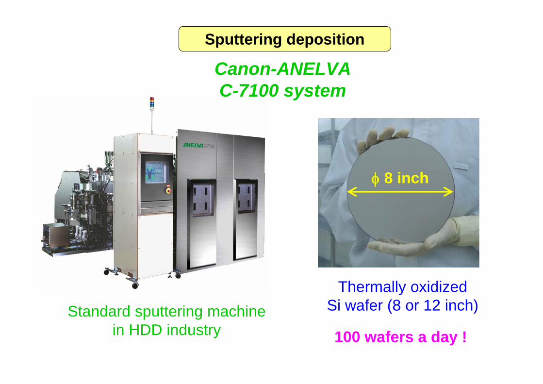
Sputtering deposition
Standard sputtering machine in HDD industry
Canon-ANELVA C-7100 system
Thermally oxidized Si wafer (8 or 12 inch)
100 wafers a day !
φ 8 inch
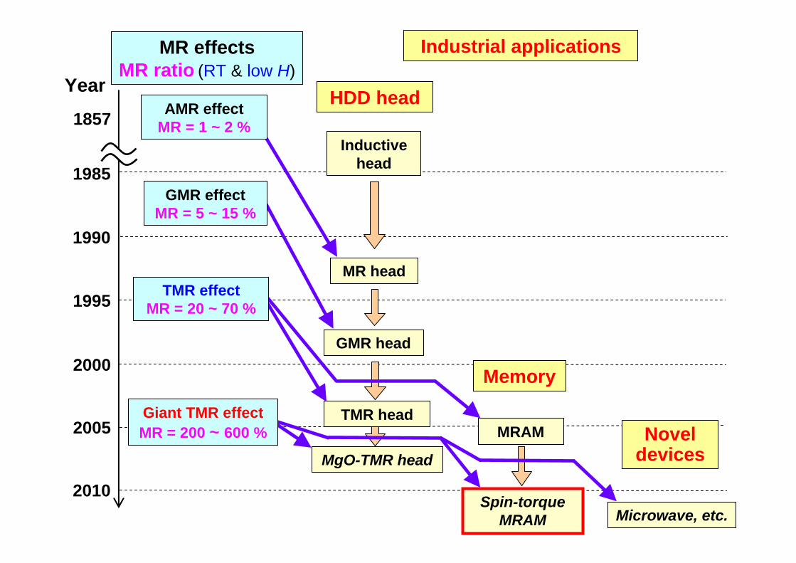
Year
1990
1995
2000
2005
2010
MR head
GMR head
HDD head
MgO-TMR head
Inductivehead
Industrial applications
MRAM
Memory
Spin-torqueMRAM
Novel devices
Microwave, etc.
AMR effect MR = 1 ~ 2 %
TMR effectMR = 20 ~ 70 %
Giant TMR effectMR = 200 ~ 600 %
1857
GMR effectMR = 5 ~ 15 %
1985
TMR head
MR effects MR ratio (RT & low H)

GMRヘッドの出現
0.01
0.1
1
10
100
1000
■■
■
■
■ ■
■■
■
■■■
■■
■■
■
■
■
■ ■
■■
■
■■■
■■
AMR GMR TMR
■■
1990 1992 1994 1996 1998 2000 2002 2004 2006 20081990 1992 1994 1996 1998 2000 2002 2004 2006 2008Year
GMR head
■
TMR head
■■■
Rec
ordi
ng d
ensi
ty (
Gbi
t/in
ch2 )
Recording medium
N SS N
N SS N
N SS N
Rotation
N SS N
N SS N
N SS N Read head
Write head
Next-generation read head is indespensablefor > 200 Gbit / inch2.
Head Medium
Technologies for HDD read head
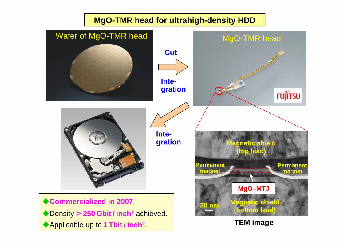
MgO-TMR head for ultrahigh-density HDD
Wafer of MgO-TMR head
TEM image
MgO-TMR head
◆Commercialized in 2007.◆Density > 250 Gbit / inch2 achieved.◆Applicable up to 1 Tbit / inch2.
Cut
Inte-gration
20 nm
Magnetic shield (top lead)
MgO–MTJ
Permanent magnet
Magnetic shield (bottom lead)
Permanent magnet
Inte-gration
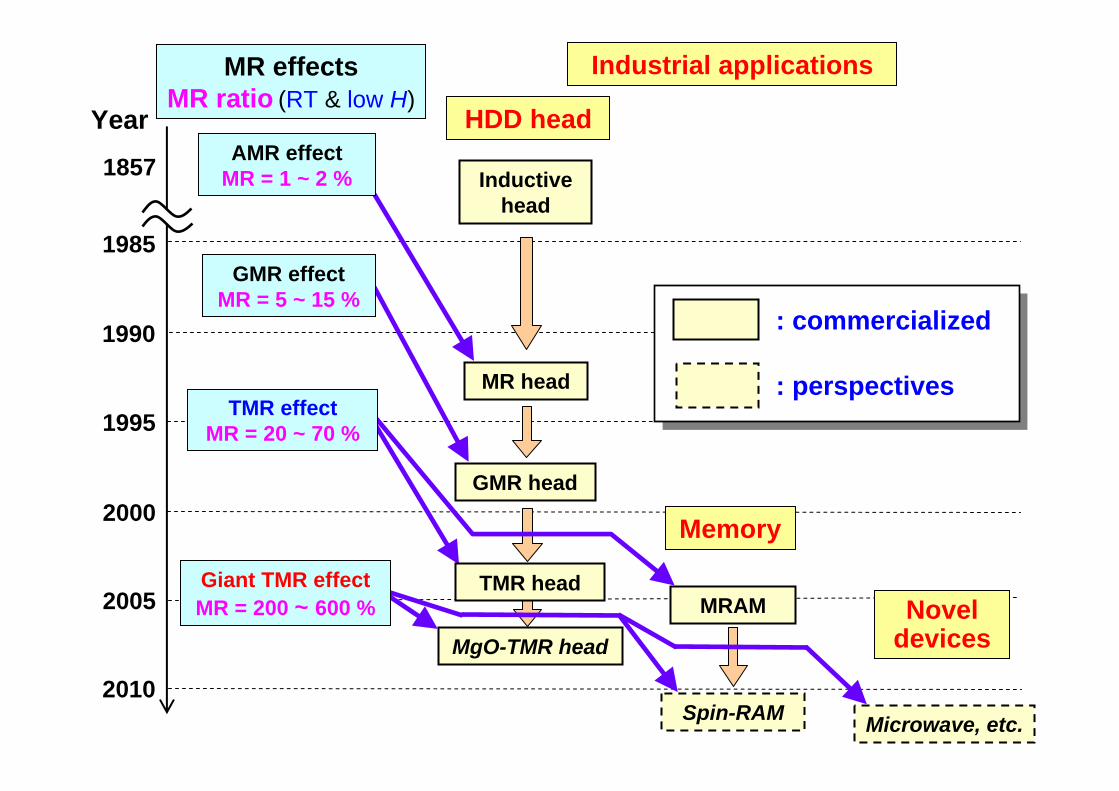
Year
1990
1995
2000
2005
2010
MR head
GMR head
HDD head
MgO-TMR head
Inductivehead
Industrial applications
MRAM
Memory
Spin-torqueMRAM
Novel devices
Microwave, etc.
AMR effect MR = 1 ~ 2 %
TMR effectMR = 20 ~ 70 %
Giant TMR effectMR = 200 ~ 600 %
1857
GMR effectMR = 5 ~ 15 %
1985
TMR head
MR effects MR ratio (RT & low H)
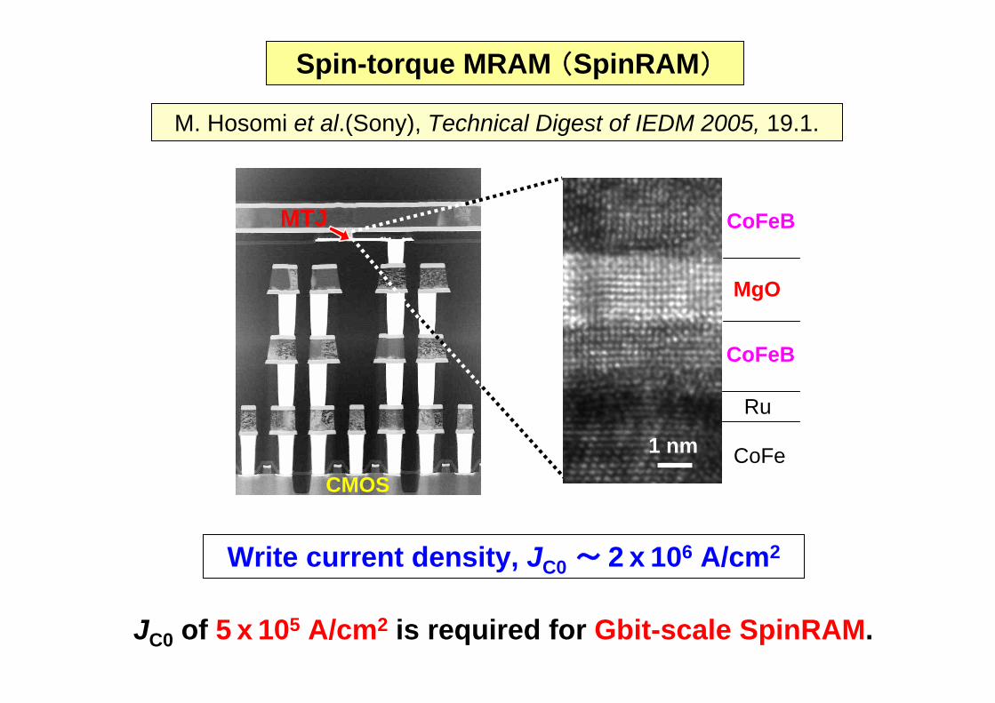
Spin-torque MRAM (SpinRAM)
MTJ
Ru
CoFe1 nm
CoFeB
MgO
CoFeB
CMOS
Write current density, JC0 ~ 2 x 10⁶ A/cm2
M. Hosomi et al.(Sony), Technical Digest of IEDM 2005, 19.1.
JC0 of 5 x 10⁵ A/cm2 is required for Gbit-scale SpinRAM.
SpinRAM having perpendicular magnetization
A CMOS integrated MTJ array
MTJ
Upper metal
Upper electrode
Bottom elctrodeReference layer
MgOStorage layer
50nm
A TEM image of 50 nm-sized MTJ
50 nm
Perpendicularly magnetized MTJ is a promising technology for
Gbit-scale Spin-RAM.
T. Kishi (Toshiba), SY et al., IEDM (2008) 12.6.
MgO(001)
or
JC0 < 106 A/cm2 achieved !
Perpendicularly-magnetized electrodes
Year
1990
1995
2000
2005
2010
MR head
GMR head
HDD head
MgO-TMR head
Inductivehead
Industrial applications
MRAM
Memory
Spin-RAM
Novel devices
Microwave, etc.
AMR effect MR = 1 ~ 2 %
TMR effectMR = 20 ~ 70 %
Giant TMR effectMR = 200 ~ 600 %
1857
GMR effectMR = 5 ~ 15 %
1985
TMR head
MR effects MR ratio (RT & low H)
: commercialized
: perspectives
: commercialized
: perspectives


![Tunnel Magnetoresistance with Atomically Thin Two ...consumption [1]. Such tunnel devices typically require growth of insulating materials of few atomic layers thin, which is a major](https://img.pdfslide.us/doc/110x75/5f4016dead667955a519a90d/tunnel-magnetoresistance-with-atomically-thin-two-consumption-1-such-tunnel.jpg)