Embed Size (px)
DESCRIPTION
Electro
Citation preview
Complementary digital logic based on the “Coulomb blockade” J. R. Tucker Lkpartmc?nt oj~Elecrrica1 and Computer Engineering and Beckman Institute, University of Illinois at ZJrhana-Cltamnpaign, Urbana, Illinois 61801
(Received 21 October 1991; accepted For publication 14 July 1992)
A finite charging energy, e”/2C’, is required in order to place a single electron onto a small isolated electrode lying between two tunnel junctions and having a total capacitance C’ to its external environment. Under suitable conditions, this elemental charging energy can effectively block all tunnel events near zero bias voltage in series arrays of ultrasmall junctions, an effect that has come to be known as the “Coulomb blockade.” This article outlines a new approach to the design of digital logic circuits utilizing the Coulomb blockade in capacitively biased double-junction series arrays. A simple “on”/“off” switch is described and complementary versions of this switch are then employed to design individual logic gates in precise correspondence with standard complementary metal-oxide semiconductor architecture. A planar nanofabrication technique is also described that may eventually allow the integration of Coulomb blockade logic onto conventional semiconductor chips, thereby realizing hybrid integrated circuits having device densities and operating speeds far in excess of present technology,
1. INTRODUCTION
It is widely recognized that the long term trend toward steadily increasing function densities in conventional inte- grated circuit.s cannot be extended indefinitely. Some argue that present semiconductor device structures cannot be usefully scaled to minimum geometries below about 0.25 pm,’ but this remains to be seen. Whatever the exact limits of conventional integrated circuit (IC) technology turn out to be, it is clear that there will still be “plenty of room at the bottom” in the sense envisioned by Feynman’ many years ago. One possibility for performing electronic func- tions at vastly higher densities involves the utilization of the Coulomb charging effects that occur when individual electrons are localized on metal islands of very small ca- pacitance and isolated between tunnel junctions. Likharev3 has proposed that tunneling of electrons across double- junction series arrays could be controlled by a bias applied at the center electrode in order to realize “transistors,” which might then be configured into logic circuits. The funct.ion densities that could theoretically be achieved are many orders of magnitude greater than the most optimistic projections of current semiconductor technology, but a practical nanolithography would need to be developed in order to realize this potential. Over the years since this possibility was first discussed, interest has remained strong in Coulomb charging effects and initial efforts toward achieving a nanometer scale lithography4 have been under- taken. It is against this background that we present a novel design for utilizing the “Coulomb blockade” effect in double-junction series arrays to implement complementary versions of a two-level “on”/“off” digital switch. Logic circuits may then be composed in direct correspondence with standard complementary metal-oxide semiconductor (CMOS) architectures. A possible planar fabrication tech- nique is also outlined. This scheme appears to have a num-
ber of practical advantages, and might serve as a focus for continued research in the direction of nanoscale electronic devices.
The importance of charging effects due to individual electrons in systems of very small particles was recognized over forty years ago by Garter,’ and convincing experi- mental evidence was obtained in measurements carried out on ultrathin granular metal films by Neugebauer and Webb.6 In 1968, Giaever and Zeller7 performed an espe- cially interesting set of experiments designed to interpret the high resistance zero-bias anomalies known to occur in many types of tunnel junctions at low temperatures. By evaporating Sn onto an oxidized Al film under conditions providing agglomeration, they were able to produce Al- oxide-Al tunnel junctions having large numbers of Sn droplets with radii -100 w imbedded inside the oxide barrier. As electrons tunneled sequentially through this structure, Coulomb charging energies for the individual droplets acted to suppress tunneling on a voltage scale given by
e 80 mV 2C’=C’0 (1)
where 1 aF= lo-‘s F and C’ represents the total capaci- tance between an individual droplet and its environment. This characteristic voltage scale corresponded to several millivolts in the Giaever-Zeller experiments, and the aver- age behavior was found to mimic the properties of the low temperature resistance peaks previously observed in many types of tunnel junctions. The temperature scale associated with the Coulomb charging energy is
2 928.5 K To=-=
2kBC’ C’(aF) ’
and these studies were carried out at liquid-I-Ie tempera- tures in order to suppress all thermal fluctuations.
4399 J. Appi. Phys. 72 (91, 1 November 1992 0021-8979/92/214399-15$04.00 $j 1992 American Institute of Physics 4399
Downloaded 26 Dec 2005 to 129.60.47.3. Redistribution subject to AIP license or copyright, see http://jap.aip.org/jap/copyright.jsp
Following closely on this work, experiments by Lambe and Jaklevic’ employed a similar fabrication technique to realize a resistor-capacitor array configuration, in which the oxide barrier between the droplets and one of the ekc- trodes was too thick to permit tunneling. Capacitance- voltage measurements clearly showed osc.illatory behavior due to quantized charging of the individual droplets in these experiments as a result of tunneling to and from the near electrode. Random charges are also induced onto the individual droplets by defects and impurities located within the oxide barriers, and Fermi levels may be offset by differences in work function. Both of these effects are some- times characterized as a random background polarization charge QP on the droplets distributed with uniform prob- ability density over the interval -e/2 < QP < e/2. Larger values are transferred into this range by tunneling of indi- vidual electrons. The capacitance-voltage oscillations due to discrete charging of the droplets were observable in the Lambe-Jaklevic experiments only because of an apparent tendency for the individual Fermi levels to become aligned through slow readjustments in Qpt and a “memory effect” was identified with the polarization changes occurring in the oxide barriers in response to an applied dc potential on a time scale of several minutes at liquid He temperatures. More recently, Cavicchi and Silsbee9 have carried out ex- tensive further experiments on droplet arrays similar to those of Lamb and Jaklevic, including a detailed study of the memory effect. This more recent work sheds important new light on the nature of the polarization occurring within the oxide barriers, and it will be discussed in some detail in Sec. VI.
Interest in Coulomb charging effects has been stimu- lated during the past few years with new theoretical pre- dictions by Averin and Likharev” and by Ben-Jacob and co-workers,” following earlier theoretical work by Kulik and Shekhter.” Experiments similar to those of Giaever and Zeller were repeated by Kuzmin and Likharev13 and by Barner and Ruggiero,‘” and these succeeded in observ- ing both the Coulomb blockade of tunneling near zero volt- age and the predicted Coulomb staircase of current steps appearing on the dc 1-V characteristic of double-junction series arrays with substantially different resistance- capacitance (RC) time constants. Van Bentum and co- workers’s further refined these experiments by utilizing the tip of a scanning tunneling microscope (STM) to inject electrons into individual Al droplets evaporated onto an oxidized Al substrate. Similar STM studies of tunneling into individual droplets were also performed by Wilkins et al. I6 and by Wan et al. l7 Data from these STM experiments on single droplets having diameters - 100 A yielded well defined “blockade” regions and sharp current steps in ex- cellent agreement with the predictions of the simplest the- oretical models, inferring junction capac.itances C< lo-‘s F in most cases.
The realization of Coulomb charging effects in the form of fabricated “device” structures had its origin in seminal work by Fulton and Dolan.18 Their tunnel junc- tion arrays were made by the shadow mask technique, with individual junc.tion areas of (0.03 =?=O.Ol pm)z and capac-
itances in the lo-r6 F range. In addition to observing the Coulomb blockade in fabricated double-junction series ar- rays, Fulton and Dolan demonstrated that these charging effects could be periodically modulated by applying a bias voltage through the substrate. This result was in agreement with predictions by Averin and Likharev,” who had ar- gued that the period of such oscillations should correspond to inducing one additional electronic charge onto the cen- ter electrode of the double-junction via a coupling capaci- tor. Work on Coulomb charging effects in fabricated arrays was extended to larger structures by Kuzmin et aI.,19 who observed the Coulomb blockade and substrate bias effects in 13-junction series arrays, again in agreement with the simplest theory. Subsequent application of microwave ra- diation onto similar 15 and N-junction series arrays by the same group”’ produced experimental evidence for the single-electron tunneling oscillations predicted” to occur at a fundamental frequency given by f =I/e.
Recently, the first “real” electronic device to utilize the Coulomb blockade effect has been reported by Geerligs et aL,‘l the so-called “electron turnstile.” This device consists of a voltage-biased series array of four identical tunnel junctions with a gate capacitor coupled to the central elec- trode lying between junctions 2 and 3. Application of a suitable positive voltage to the gate capacitor induces tun- neling out of the negative supply terminal and across junc- tions 1 and 2, causing a single extra electron to occupy the central island. Returning the gate voltage to its original level then expels this electron into the positive supply ter- minal through junctions 3 and 4, resulting in the passage of one electronic charge through the “turnstile” for each cy- cle of the gate voltage. Accurate quantization of the cur- rent at values I=ef proportional to the applied gate fre- quency f was observed in the MHz region. Relatively large junction capacitances C- 1O-‘5 F were used, however, so that the temperature needed to be reduced to -20 mK in order to completely suppress all thermal tunnel events which could otherwise spoil the current quantization.
The success of the electron turnstile has led to renewed interest in possible electronic. applications of the Coulomb blockade. Likharev3 initially proposed that double junc- tions be used as transistors, with current flow controlled by capacitive or resistive coupling to the center electrode. More recently, Likharev and co-workers”” have focused on alternative schemes for digital logic in which individual electronic charges represent the logic states appearing on the inputs and outputs of the various gates. While such schemes are conceptually elegant, there are serious practi- cal difficulties which would need to be overcome. First., the operating temperatures must be limited to T < To/100 in order to prevent a single thermally generated tunnel event from spoiling the entire calculation. Even under the as- sumption that nanolithographic techniques might someday produce fabricated tunnel junctions with capacitance val- ues C- 10-r* F, this requirement will nevertheless corre- spond to temperatures at or below the liquid-He range according to Eq. (2 ). In addition, requiring that the output of a single electron from one logic gate be capable of charg- ing the inputs of all subsequent gates plus the associated
4400 J. Appi. Phys., Vol. 72, No. 9, 1 November 1992 J. R. Tucker 4400
Downloaded 26 Dec 2005 to 129.60.47.3. Redistribution subject to AIP license or copyright, see http://jap.aip.org/jap/copyright.jsp
interconnections could be problematic. Any stray capaci- tance occurring within the interconnections between the gates would need to be kept negligible compared to the capacitances of the tunnel junctions themselves. Further- more, the design rules for such circuits would need to be altered for different numbers of following gates (fan out] in a complicated fashion. While this version of “single elec- tronics” may eventually become possible, it places espe- cially severe requirements on both the fabrication technol- ogy and the operating temperature.
The logic concept described in this paper returns to Likharev’s original idea of utilizing the double junction as a transistor. The difference here is a novel capacitive bias- ing arrangement which permits the design of simple onloff digital switches. Complementary versions of this double- junc.tion switch are used to connect the outputs of logic gates directly to the supply terminals, as in conventional CMOS technology. This scheme is therefore much more robust, because it can be designed so that a sizeable num- ber of electrons must be passed through the switches in order to charge subsequent gates and interconnects to the supply voltages. Eliminating all stray capacitance is no longer a critical design problem, and much higher operat- ing temperatures bec.ome possible. The cost of these prac- tical advantages is a substantial reduction in speed com- pared with circuits in which data is represented by individual charges, since more electrons must be passed through the switches. We wish to emphasize from the be- ginning that our purpose here is not to criticize the general concept of logic based on single electrons, but only to sug- gest an alternative design that may prove easier to imple- ment in the near term.
Prototype circuits containing one or a few logic gates of the type described here can be fabricated today. At the present limits of lithography, however, the capacitances of individual fabricated tunnel junctions are still relatively large, with C- lo-lb F. Because the total capacitance of the center electrode in our double-junction switches is de- signed to be roughly an order of magnitude larger than that of the smallest singIe junction, Eq. (2) implies that such circuits would need to be tested at temperatures T < 1 K. Relatively small numbers of logic gates are also implied by the need to individually adjust the capacitive bias volt- age of each isolated electrode in order to cancel the effects of random background polarization charges, as was done in the case of the electron turnstile device. Future progress in nanolithography, however, may make it possible to fab- ricate much smaller tunnel junctions having capacitances C<lOJ’s F, similar to the - lOO-A-diam metal droplets employed in recent STM experiments. These values of ca- pacitance could raise the operating temperature to 77 K, and perhaps even to room temperature. In addition, con- trolled fabrication techniques could potentially eliminate the effects of random bac.kground polarization charges en- tirely, opening the way to large-scale integrated circuits.
The technological driving force behind efforts to im- prove lithographic resolution is the tremendous increase in function density which might someday be achieved with nanometer scale electronic devices. Coulomb charging ef-
+e-
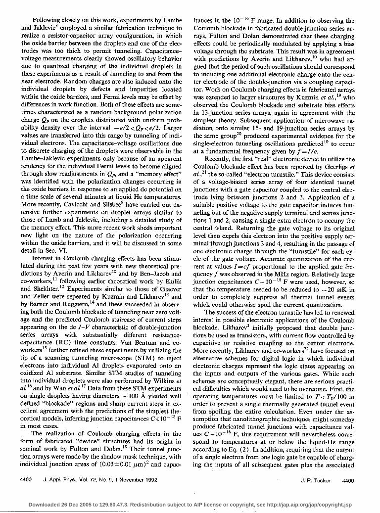
FIG. 1. Current-biased single junction with ohmic resistance R and ca- pacitance C. Forward tunneling of electronic charges +@ discretely re- duces the junction charge according to Q- (Q-e).
fects will become increasingly important as device dimen- sions are reduced, and they are expected to play a domi- nant role at the nanometer level. Single-electron charging phenomena are already being observed in GaAs double- pinch-gate structures having center islands with dimen- sions as large as 1 pm.“” Given the inevitability of this situation, it is natural to think in terms of utilizing the Coulomb blockade effect as a basis for implementing logic circ.uits at very high densities. Since tunnel junctions are perhaps the most compact of all electronic devices, it is theoretically possible to create a double-junction switch or even a complete logic gate within an area smaller than [ 100 A),’ corresponding to function densities > 10” cme2 and fundamental charging energies )O.l V. Such small capacitances imply very high speeds
RC=O.l psxR(100 kn)XC(aF) (31
even though junction resistanc.es must always be kept large compared to the “quantum of resistance,” RQ=h/4e2z6.5 kfiZ, in order to suppress tunneling by quantum fluctua- tions. Thii potential combination of speed and function density is so striking that it is difficult to imagine any other alternative electronic technology that could match the long-term possibilities of the Coulomb blockade in these areas.
Sections II and III of this article will review basic as- pects of the Coulomb blockade effect in current-biased sin- gle junctions and voltage-biased double junctions, respec- tively. Section IV describes the design of a digital on/off logic switch based on the capacitively biased double- junction configuration. Section V utilizes this switch and its complement to compose an inverter circuit and other logic gates by direct analogy with standard CMOS archi- tecture. Section VI discusses a planar nanofabrication tech- nique which might eventually be employed to integrate Coulomb blockade logic onto conventional semiconductor circuits, followed by a brief conclusion in Sec. VII.
II. CURRENT-BIASED SINGLE JUNCTION
Consider an isolated tunnel junction with resistance R and capacitance C, as illustrated in Fig. 1. Effects due to discrete transfer of charge between the electrodes become important when the elemental charging energy e2/2C is
4401 J. Appl. Phys., Vol. 72, No. 9, 1 November 1992 J. FL Tucker 4401
Downloaded 26 Dec 2005 to 129.60.47.3. Redistribution subject to AIP license or copyright, see http://jap.aip.org/jap/copyright.jsp
greater than the thermal energy k,T. In addition, the tun- neling resistance must be large compared to the quantum of resistance, Rp=h/4e’z6.5 kfi, in order to insure that quantum fluctuations with energies - h/RC are also small compared to e’/2C.
When subjected to a current bias, as indicated in Fig. 1, the junction’s charge Q will be incremented continuously, by the current source and drained discreteIy by tunneling of electrons in the forward direction
Q= JI, I dt--ne. (4)
The net number of electrons that have tunneled across the junction is represented by n, which may be taken as the difference pt = n + - n _ between forward and reverse events. Here the sign of the electron charge is chosen to be positive in order to forestall confusion associated with the usual negative sign convention. This should cause no problem, as long as we remember that the upstream electrode will ac- tually be negative in practice.
Forward tunnel events will be designated with a ( + ) sign, and these act to reduce the junction charge according to Q-Q-e. It will be assumed that the time scale of an individual tunnel event is instantaneous compared with the rate at which Q is incremented by the current source. The electrostatic energy liberated during a forward tunnel event will then be given by
AFt (Q) =Q?-(Q-e’2 ’ e2
2c ZC=e--- c 2C’ (5) The first term on the right is the product of the electron charge and the junction voltage, V=Q/C, as it is usually defined. The second term is a “Coulomb correction” due to the finite electron charge that must be included for junc- tions of very small capacitance under the conditions de- scribed above. The quantity AF+(Q) represents the in- crease in free energy imparted to an electron during a forward tunnel event, We can express this as an effective voltage for forward tunneling, Vf = AF’/e, which is seen to be reduced by Coulomb charging effects
V+(n)=V(n)-;. (6)
Note that the voltage V(n) =Q(n)/C appearing across the junction depends upon the net number of electrons that have previously tunneled across the barrier through Eq. (4). For Q < e/2 or Y< e/2C, the final state is seen to have higher free energy than the initial state, and forward tran- sitions will therefore not be possible over this range in the low temperature limit T-SO.
Reverse tunnel events will be designated with a ( -) sign. They increase the junction charge according to Q-Q +e, changing the electrostatic energy according to
&7-(Q) =$-‘Q2;)2 ’ e2 -=-eC-2C*
(7)
Reverse transitions thus produce a higher final state elec- trostatic energy for junction charges Q> -e/2 or voltages
4402 J. Appl, Phys., Vol. 72, No. 9, 1 November 1992
V > - ei2C, and this extra free energy - AF- (Q) must be supplied by the tunneling electron. The quantity - AF-(Q) thus represents the decrease in the tunneling electron’s energy with respect to the Fermi level upon en- tering the upstream electrode. An effective voltage for re- verse transitions may therefore be defined according to V- = - A.F-/e, which is seen to be increused by the Coulomb charging effects
v-(n)=V(n)+$. (8)
In the low temperature limit T-+0, reverse tunnel events are possible only when this quantity is negative (positive AFL ) for junction voltages Y< - e/2C. Since forward events are possible only for I’> e12C at low temperatures, all transitions will be suppressed by a Coulomb blockade over the voltage range -e/2C < 1’ i e/2C, corresponding to junction charges -e/2 < Q < e/2.
The concept of an effective voltage defined separately for forward and reverse transitions leads immediately to simple expressions for the tunneling rates. Suppose t.hat the ordinary dc I-Y characteristic for the junction lit V) has been measured or calculated under voltage-biased condi- tions. An ideal voltage source will maintain a constant charge Q=CV on the junction capacitance, instanta- neously compensating for fluctuations occurring as a result of tunnel events. Under these conditions, the Coulomb charging energy of the junction will not change during tunneling transitions, and the effective voltages for both forward and reverse directions will be equal and given by the externally applied source. Plasma frequencies for good metals lie in the ultraviolet region, wP.- 10” s-‘, and are thus much greater than inverse tunneling times by any reasonable estimate, so that this condition is easily realized in practice. At finite temperatures, the net current flowing through a voltage-biased tunnel junction will represent a difference between forward and reverse components. It is easy to show that the ratio of these two components is given by a Boltzmann factor, exp( -eF’/kT), so that
IjC V ‘:“)‘[*-exp(-e~~,~*)1 ’
and
I,~c v) =Ijt r k )exp( --eVikT) [I-exp(-eF’/l/kT)l ’
(9)
(10)
with Jj( Y) =I]+ ( Y) --I,: ( V). When the junction is cur- rent biased, so that the charge on the electrodes must change by *e during tunnel events, the effective voltages for forward and reverse transitions will no longer be equal due to the Coulomb charging correction, with V*(n) = V( tt) F e/2C. The forward and reverse transition rates are then given by
r*(Q)=e--.‘rli”[V(n)re/2C]. (11)
These results for the forward and reverse transition
J. FL Tucker 4402
Downloaded 26 Dec 2005 to 129.60.47.3. Redistribution subject to AIP license or copyright, see http://jap.aip.org/jap/copyright.jsp
v = ;( Jiit- ne) v n=-lv n_~s~~ 0
Td . . . i,LK/Z.S ri P n=O-1
n = 0 v ----* ..&, i,, /Sri /i, 1 e/C
- -42c
+--iF
el-+
n=+l,d er- -e/2C n=2-1
n = + 2 , - 4 /
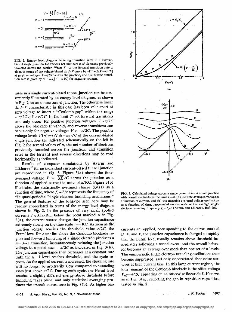
FIG. 2. Energy level diagram depicting transition rates in a current- biased single junction for various net numbers n of electrons previously tunneled across the barrier. When T-+0, the forward transition rate is given in terms of the voltage-biased dc I-Y curve by el? ’ =IJV-e/Xl at positive voltages F’=Q/C across the junction, and the reverse transi- tion rate is given by eT =I,CV+JZq for negative voltages.
l-GrS
1.0 -
-I- r - s
s
F E
D c ‘-4 Y-G
A B ( >
0 0 0.5 1.0 I
rates in a single current-biased tunnel junction can be con- veniently illustrated by an energy level diagram, as shown in Fig. 2 for an ohmic tunnel junction. The otherwise linear dc I-Y characteristic in thii case has been split apart at zero voltage to insert a “Coulomb gap” within the range -e/26< Y< e/2C. In the limit T-+0, forward transitions can only occur for positive junction voltages V>e/2C above the blockade threshold, and reverse transitions can occur only for negative voltages V< -e/2C. The possible voltage levels V(n) = (JI dt- ne)/C of the current-biased single junction are indicated schematically on the left in Fig. 2 for several values of n, the net number of electrons previously tunneled across the junction, and transition rates in the forward and reverse directions may be read horizontally as indicated.
Results of computer simulations by Averin and Likharev’” for an individual current-biased tunnel junction are reproduced in Fig. 3. Figure 3 (a) shows the time- averaged voltage V = {Q>/C across the junction as a function of applied current in units of e/RC. Figure 3 (b) illustrates the statistically averaged charge {Q(t)) as a function of time, whereJ$=l/e represents the frequency of the quasi-periodic “single electron tunneling oscillations.” The general features of the behavior seen here may be readily appreciated in terms of the energy level diagram shown in Fig. 2. In the presence of very small applied currents I < O.le/RC, below the point marked A in Fig. 3 (a), the current source charges the junction capacitance extremely slowly on the time scale ry RC. As soon as the junction voltage reaches the threshold value e/2C, the Fermi level for N = 0 lies above the Coulomb blockade re- gion and forward tunneling of a single electron produces a n==O--r 1 transition, instant.aneously reducing the junction voltage to a point near --e/2C as indicated in Fig. 3(b). The junction capacitance then recharges at a constant rate until the n= 1 level reaches threshold, and the cycle re- peats. As the applied current is increased, the charging rate will no longer be arbitrarily slow compared to tunneling rates just above e/2C. During each cycle, the Fermi level reaches a slightiy different energy above threshold before tunneling takes place, and only statistical averaging pro- duces the smooth curves seen in Fig. 3(b). As higher bias
5
(a)
FIG. 3. Calculated voltage across a single current-biased tunnel junction with normal electrodes in the limit T-0: (a) the time-averaged voltage as a function of current, and (b) the ensemble-averaged voltage oscillations as a function of time, represented on the scale of the average single- electron tunneling frequency f,= IJe (Averin and Likharev, Ref. 10).
currents are applied, corresponding to the curves marked D, E, and F, the junction capacitance is charged so rapidly that the Fermi level usually remains above threshold im- mediately following a tunnel event, and the overall behav- ior becomes an average over more than one set of n levels. The semiperiodic single electron tunneling oscillations then become suppressed, and only uncorrelated shot noise sur- vives at high current bias. In this large current regime, the lone remnant of the Coulomb blockade is the offset voltage V&= e/2C appearing on an otherwise linear dc I-V curve, as in Fig. 3(a), reflecting the gap in transition rates illus- trated in Fig. 2.
4403 J. Appl. Phys., VoL 72, No. 9, 1 November 1992 J. R. Tucker 4403
Downloaded 26 Dec 2005 to 129.60.47.3. Redistribution subject to AIP license or copyright, see http://jap.aip.org/jap/copyright.jsp
T
+u
CO
+v~ hG1 R2J2
+e- +e-
--I =
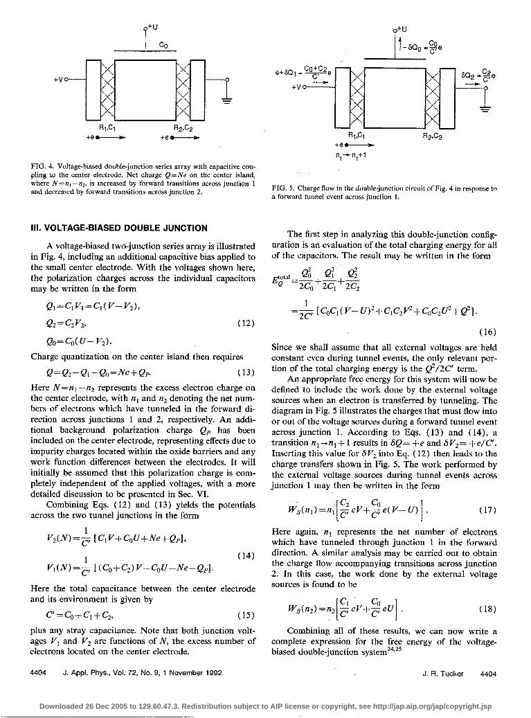
FIG. 4. Voltage-biased double-junction series array with capacitive cou- pling to the center electrode. Net charge Q=We on the center island, where N=n, --n,, is increased by forward transitions across junction 1 and decreased by forward transitions across junction 2.
HI. VOLTAGE-BIASED DOUBLE JUNCTION
A voltage-biased two-junction series array is illustrated in Fig. 4, including an additional capacitive bias applied to the small center electrode. With the voltages shown here, the polarization charges across the individual capacitors may be written in the form
Q,=C,V,=C,( V- V2),
Q2= C2V29 (12)
Qo=CoC u- Vd. Charge quantization on the center island then requires
Q=Qz--QI-Qo=Ne+Qp (131
Nere N=E, -n2 represents the excess electron charge on the center electrode, with ?I, and 1z2 denoting the net num- bers of electrons which have tunneled in the forward di- rection across junctions 1 and 2, respectively. An addi- tional background polarization charge QP has been included on the center electrode, representing effects due to impurity charges located within the oxide barriers and any work function differences between the eiectrodes. It will initially be assumed that this polarization charge is com- pletely independent of the applied voltages, with a more detailed discussion to be presented in Sec. VI.
Combining Eqs. ( 12) and (13) yields the potentials across the two tunnel junctions in the form
WV=&, [C, V+Gf-f+Ne+Qpl,
V,(N)=; [(Co-kC2)V-C&J-Ne-Q,]. (I.41
Here the total capacitance between the center electrode and its environment is given by
C’=co+C1+C2, (15) plus any stray capacitance. Note that both junction volt- ages VI and t’Z are functions of N, the excess number of electrons located on the center electrode.
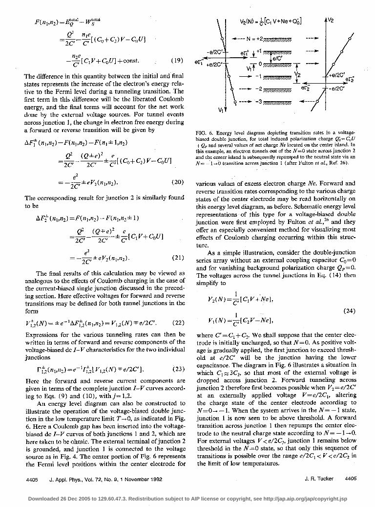
nl- n,+l
FIG. 5. Charge flow in the double-junction circuit of Fig. 4 in response to a forward tunnel event across junction 1.
The first step in analyzing this double-junction config- uration is an evaluation of the total charging energy for all of the capacitors. The result may be written in the form
peal- Qi I Qi I Qi 0 zc, 2q 2c,
=& [c,c,(v-u)2+c,c,vz+c*c,u2+e”].
Since we shall assume that all external voltages are held constant even during tunnel events, the only relevant por- tion of the total charging energy is the @/2C’ term.
An appropriate free energy for this system will now be defined to include the work done by the external voltage sources when an electron is transferred by tunneling. The diagram in Fig. 5 illustrates the charges that must flow into or out of the voltage sources during a forward tunnel event across junction 1. According to Eqs. (13) and (14), a transition ni-+nl+- 1 results in SQ= +e and SF’,= $-e/C’. Inserting this value for SV, into Eq. ( 12) then leads to the charge transfers shown in Fig. 5. The work performed by the external voltage sources during tunnel events across junction 1 may then be written in the form
I G G Wslnl)=~~ ceV-f-pe(V--17) 1 .
Here again, ~-2~ represents the net number of electrons which have tunneled through junction 1 in the forward direction. A similar analysis may be carried out to obtain the charge flow accompanying transitions across junction 2. In this case, the work done by the external voltage sources is found to be
W&z) =?.Q i Cl CO ~eV-+eU = 1
Combining all of these results, we can now write a complete expression for the free energy of the voltage- biased double-junction system”4,25
4404 J. Appl. Phys., Vol. 72, No. 9, 1 November 1992 J. R. Tucker 4404
Downloaded 26 Dec 2005 to 129.60.47.3. Redistribution subject to AIP license or copyright, see http://jap.aip.org/jap/copyright.jsp
--!$;I C’ V+C,U] +const. (19)
The ditference in this quantity between the initial and final states represents the increase of the electron’s energy rela- tive to the Fermi level during a tunneling transition. The first term in this difference will be the liberated Coulomb energy, and the tinal terms will account for the net work done by the external voltage sources. For tunnel events ac.ross junction 1, the change in electron free energy during a forward or reverse transition will be given by
AF~(q,n2) =F(nl,n2) -F(q f l,nz)
@ (Q&e)’ e =---
2C’ 26” *$G+G) ~-GUI 2
=-&T&z*&). (20)
The corresponding result for junction 2 is similarly found to be
@ (QFe)2 e =--
2C’ 2C’ -*,cc,?r+co~l *. 1
=-L’eVz(n’,?K& 2C’ (21)
The final results of this calculation may be viewed as analogous to t.he effects of Coulomb charging in the case of the current-biased single junction discussed in t.he preced- ing section. Here effective voltages for forward and reverse transitions may be defined for both tunnel junctions in the fOK.-Kll
Vt2(M)= *e*-‘AF~Z(nl,nz)= VI,?(N) re/2C’. (22)
Expressions for the various tunneling rates can then be written in terms of forward and reverse components of the voltage-biased dc I-V characteristics for the two individual junctions
J?;f2(nl,n2) =e”““I&[ V’,:(N) Fe/2C’]. (23)
Here the forward and reverse current components are given in terms of the complete junction I-V curves accord- ing to Eqs. (9) and (lo), withj=1,2.
An energy level diagram can also be constructed to illustrate the operation of the voltage-biased double junc- tion in the low temperature limit T-0, as indicated in Fig. 6. Here a Coulomb gap has been inserted into the voltage- biased dc I--G- curves of both junct.ions 1 and 2, which are here taken to be ohmic. The external terminal of junc.tion 2 is grounded, and junction 1 is connected to the voltage source as in Fig. 4. The center portion of Fig. 6 represents the Fermi level positions within the center electrode for
\I V*(N) = &[C, V+Ne+Qb]
FIG. 6. Energy level diagram depicting transition rates in a voltage- biased double junction, for total induced polarization charge Q+C(,U + QP and several values of net charge Ne located on the center island. In this example, an electron tunnels out of the N=O state across junction 2 and the center island is subsequently repumped to the neutral state via an N= - 1 -+O transition across junction 1 (after Fulton et al., Ref. 26).
various values of excess electron charge Ne. Forward and reverse transition rates corresponding to the various charge states of the center electrode may be read horizontally on this energy level diagram, as before. Schematic energy level representations of this type for a voltage-biased double junction were first employed by Fulton et ai.,‘6 and they offer an especially convenient method for visualizing most effects of Coulomb charging occurring within this struc- ture.
As a simple illustration, consider the double-junction series array without an external coupling capacitor Co=0 and for vanishing background polarization charge QP=O. The voltages across the tunnel junctions in Eq. ( 14) then simplify to
Vd3) =&[C, y;Ivel,
(241
where C’ = Ct f C,. We shall suppose that the center elec- trode is initially uncharged, so that N= 0. As positive volt- age is gradually applied, the first junction to exceed thresh- old at e/2C’ will be the junction having the lower capacitance. The diagram in Fig. 6 illustrates a situation in which C1= 3C,, so that most of the external voltage is dropped across junction 2. Forward tunneling across junction 2 therefore first becomes possible when Vt = e/2C’ at an externally applied voltage V=e/2C,, altering the charge state of the center electrode according to N=O- - 1. When the system arrives in the N= - 1 state, junction 1 is now seen to be above threshold. A forward transition across junction 1 then repumps the center elec- trode to the neutral charge state acc.ording to N= - 1 -+O. For external voltages V < e/2& junction 1 remains below threshold in the N=O state, so that only this secptence of transitions is possible over the range e/2C, <: V < e/ZC, in the limit of low temperatures.
4305 J. Appl. Phys., Vol. 72, No. 9, I November 1992 J. PI. Tucker 4405
Downloaded 26 Dec 2005 to 129.60.47.3. Redistribution subject to AIP license or copyright, see http://jap.aip.org/jap/copyright.jsp
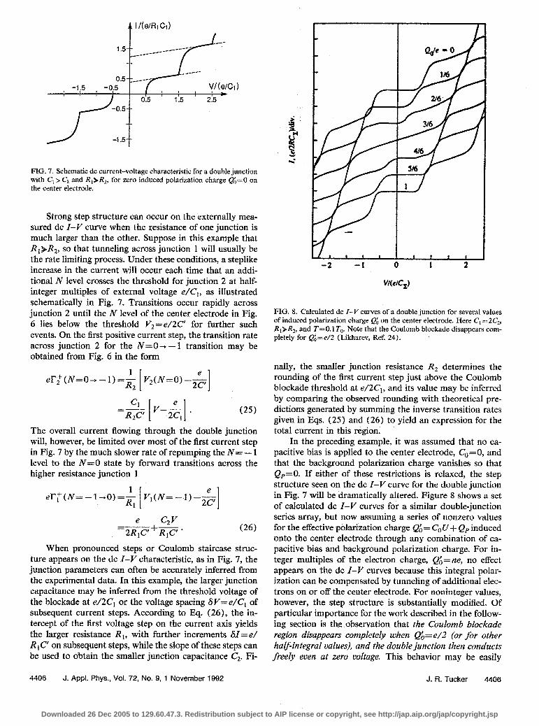
4 I/(e/RtCl)
FIG. 7. Schematic dc current-voltage characteristic for a double junction with C! > Cz and RI>R2, for zero induced polarization charge Qh=O on the center electrode.
Strong step structure can occur on the externally mea- sured dc I-V curve when the resistance of one junction is much larger than the other. Suppose in this example that R1)R2, so that tunneling across junction 1 will usually be the rate limiting process. Under these conditions, a steplike increase in the current will occur each time that an addi- tional N level crosses the threshold for junction 2 at half- integer multiples of external voltage e/C,, as illustrated schematically in Fig. 7. Transitions occur rapidly across junction 2 until the N level of the center electrode in Fig. 6 lies below the threshold VZ=e/2C’ for further such events. On the first positive current step, the transition rate across junction 2 for the N=O- - 1 transition may be obtained from Fig. 6 in the form
er$ (N=O+ - 1) =& V#V=O) -& 1 I
=& VT&. 2 1 I I The overall current flowing through the double junction will, however, be limited over most of the first current step in Fig. 7 by the much slower rate of repumping the N= - 1 level to the N=O state by forward transitions across the higher resistance junction 1
er:(N=-Lo)=~ V,(N=-1)~& R l 1 I e C2V
=2RIC’+R,C’ *
When pronounced steps or Coulomb staircase struc- ture appears on the dc I-V characteristic, as in Fig. 7, the junction parameters can often be accurately inferred from the experimental data. In this example, the larger junction capacitance may be inferred from the threshold voltage of the blockade at e/2C, or the voltage spacing GV=e/C, of subsequent current steps. According to Eq. (26), the in- tercept of the first voltage step on the current axis yields the larger resistance R i, with further increments H=e/ R i C’ on subsequent steps, while the slope of these steps can be used to obtain the smaller junction capacitance Cz. Fi-
z 1
FIG. 8. Calculated dc I-V curves of a double junction for several values of induced polarization charge Q: on the center de&rode. Here C, = 2C,, R,>R,, and T=O.l T,. Note that the Coulomb blockade disappears om- pletely for QA=e/Z [Likharev, Ref. 24).
nally, the smaller junction resistance R2 determines the rounding of the first current step just above the Coulomb blockade threshold at e/2C,, and its value may be inferred by comparing the observed rounding with theoretical pre- dictions generated by summing the inverse transition rates given in Eqs. (25) and (26) to yield an exm-ession for the total current in this region.
In the preceding example, it was assumed that no ca- pacitive bias is applied to the center electrode, C,,=O, and that the background polarization charge vanishes so that QP=O. If either of these restrictions is relaxed, the step structure seen on the dc I-V curve for the double junction in Fig. 7 will be dramatically altered. Figure 8 shows a set of calculated dc I-V curves for a similar double-junction series array, but now assuming a series of nonzero values for the effective polarization charge QI, = C, U + QP induced onto the center electrode through any combination of ca- pacitive bias and background polarization charge. For in- teger multiples of the electron charge, QA=ne, no effect appears on the dc I-V curves because this integral polar- ization can be compensated by tunneling of additional elec- trons on or off the center electrode. For noninteger values, however, the step structure is substantially modified. Of particular importance for the work described in the follow- ing section is the observation that the Coulomb blockade region disappears completely ujhen Qh=e/2 (or jbr other half-integral values), and the double junction then conducts
freely even at zero voltage. This behavior may be easily
4406 J. Appl. Phys., Vol. 72, No. 9, 1 November ‘1992 J. R. Tucker 4406
Downloaded 26 Dec 2005 to 129.60.47.3. Redistribution subject to AIP license or copyright, see http://jap.aip.org/jap/copyright.jsp
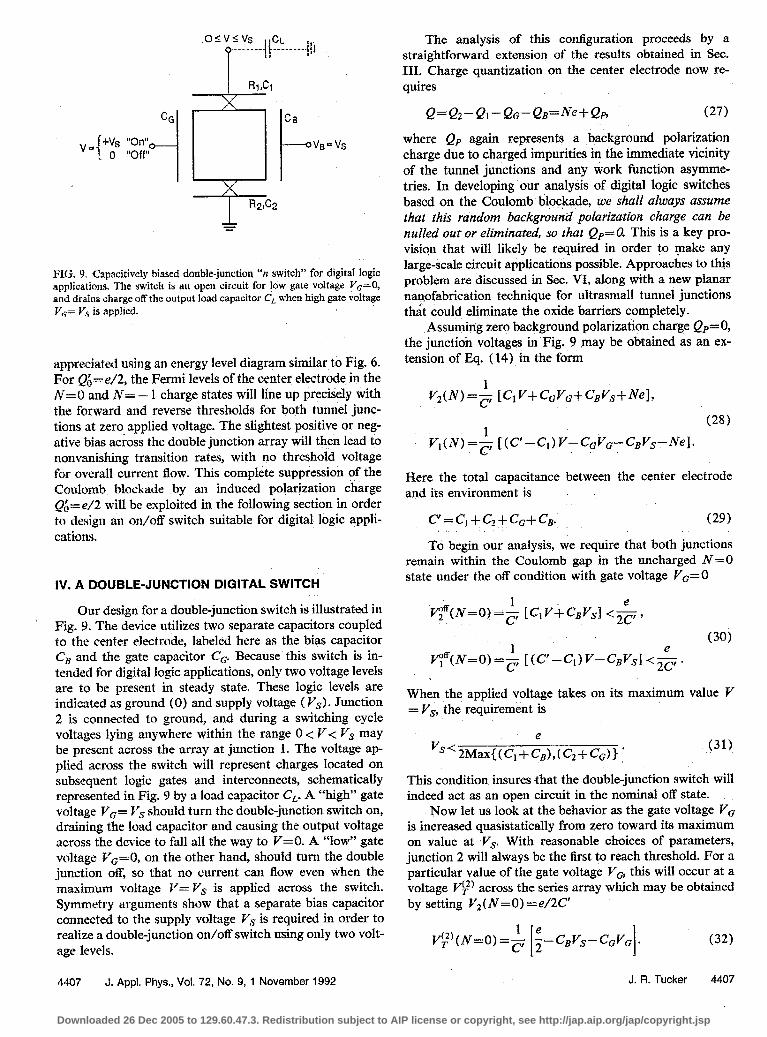
CO T+Vs “On”+..,- I 0 “Off”
v=
O~VlVs CL y ______- if ---- ----#]
RI ,Ci
~
ce
I-
VB=%
R2*C2
=
PIG. 9. Capacitively biased double-junction ‘% switch” for digital logic applications. The switch is an open circuit for low gate voltage V,=O, and drains charge off the output load capacitor CL when high gate voltage VcT= & is applied.
appreciated using an energy level diagram similar to Fig. 6. For Q;)==-P/~, the Fermi levels of the center electrode in the N=O and N== - 1 charge states will line up precisely with the forward and reverse thresholds for both tunnel junc- tions at zero applied voltage. The slightest positive or neg- ative bias across the double junction array will then lead to nonvanishing transition rates, with no threshold voltage for overall current flow. This complete suppression of the Coulomb blockade by an induced polarization charge Q,$=e/2 will be exploited in the following section in order to design an on/off switch suitable for digital logic appli- cations.
IV. A DOUBLE-JUNCTION DIGITAL SWITCH
Our design for a double-junction switch is illustrated in Fig. 9. The device utilizes two separate capacitors coupled to the center electrode, labeled here as the bias capacitor C, and the gate capacitor C,. Because this switch is in- tended for digital logic applications, only two voltage levels are to be present in steady state. These logic levels are indicated as ground (0) and supply voltage ( V,). Junction 2 is connected to ground, and during a switching cycle voltages lying anywhere within the range 0 < V< ?‘s may be present across the array at junction 1. The voltage ap- plied across the switch will represent charges located on subsequent logic gates and interconnects, schematically represented in Fig. 9 by a load capacitor C.‘,. A “high” gate voltage t;;= V, should turn the double-junction switch on, draining the load capacitor and causing the output voltage across the device to fall all the way to V=O. A “low” gate voltage rrG=O, on the other hand, should turn the double junction off, so that no current can flow even when the maximum voltage Y= V, is applied across the switch. Symmetry arguments show that a separate bias capacitor connected to the supply voltage V, is required in order to realize a double-junction on/off switch using only two volt- age levels.
The analysis of this configuration proceeds by a straightforward extension of the results obtained in Sec. III. Charge quantization on the center electrode now re- quires
Q=Qz-Qt-QG-QB=Ne+Qp (27)
where QP again represents a background polarization charge due to charged impurities in the immediate vicinity of the tunnel junctions and any work function asymme- tries. In developing our analysis of digital logic switches based on the Coulomb blockade, we shall always assume that this rundom background polarization charge cart be nuiied out or eliminated, so that QP=O. This is a key pro- vision that will likely be required in order to make any large-scale circuit applications possible. Approaches to this problem are discussed in Sec. VI, along with a new planar nanofabrication technique for ultrasmall tunnel junctions th& could eliminate the oxide barriers completely.
Assuming zero background polarization charge QP= 0, the junction voltages in Fig. 9 may be obtained as an ex- tension of Eq. ( 14) in the form
VI(N)=& [(C-C,) V-CGVG--C,Vs-Ne].
Here the total capacitance between the center electrode and its environment is
c’ = c, + c,+ c,+ c,. (29)
To begin our analysis, we require that both junctions remain within the Coulomb gap in the uncharged N=O state under the off condition with gate voltage V,=O
t”3’(N=o) =&, [c, v+c,v,] <& , (30)
qff(N=o,=$, [(cr-c,)v-C,v,] <&.
When the applied voltage takes on its maximum value Y = V,, the requirement is
e ‘~‘2Max{(C,+C,),(C,+CG’)} * (31)
This condition insures that the double-junction switch will indeed act as an open circuit in the nominal off state.
Now let us look at the behavior as the gate voltage Vo is increased quasistatically from zero toward its maximum on value at Vs. With reasonable choices of parameters, junction 2 will always be the first to reach threshold. For a particular value of the gate voltage Vo, this will occur at a voltage p:) across the series array which may be obtained by setting V,(N=O) =e/2C’
v(,2,(N=0)=&
1
~-c~v~--c,vG * 1 4407 J. Appl. Phys., Vol. 72, No. 9, I November 1992 J. FL Tucker 4407
Downloaded 26 Dec 2005 to 129.60.47.3. Redistribution subject to AIP license or copyright, see http://jap.aip.org/jap/copyright.jsp
V/V St VF’(N - 0)
0.1875
0 0.375.e’ 0.625 1.0
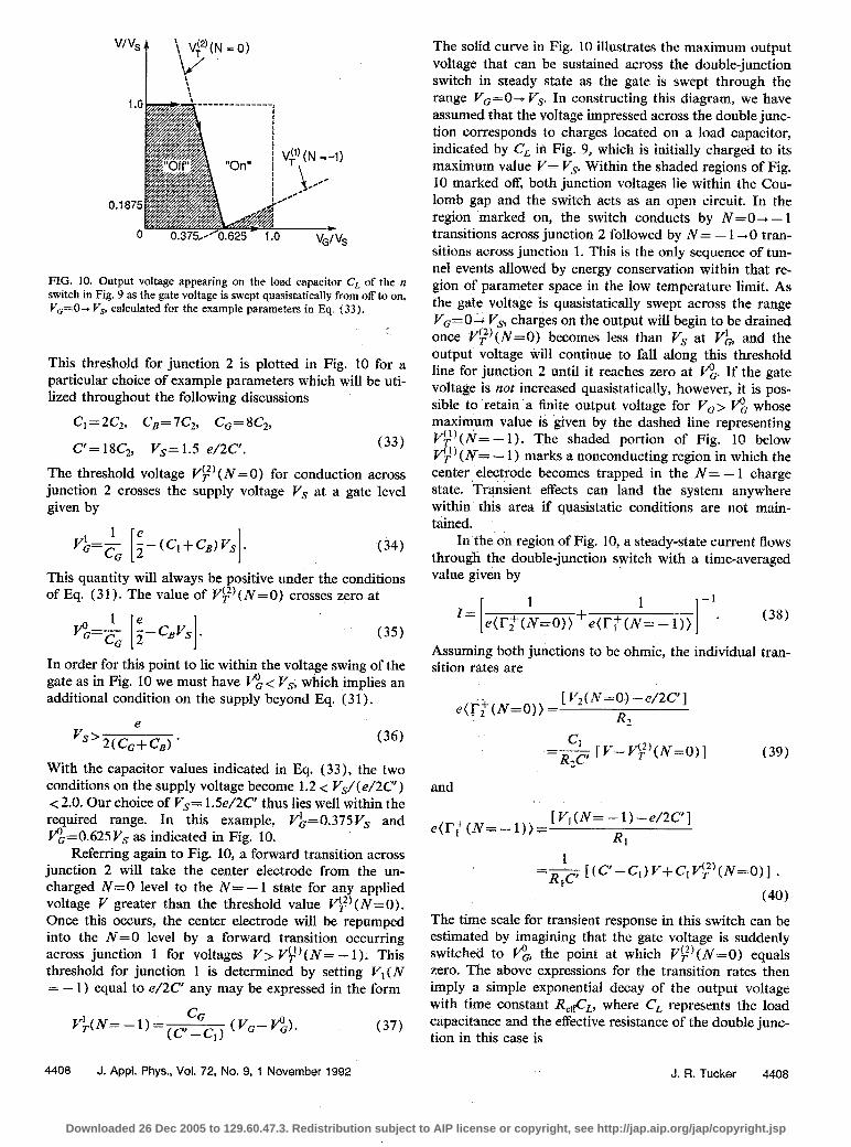
FIG. 10. Output voltage appearing on the load capacitor CL of the n switch in Fig. 9 as the gate voltage is swept quasistatically from off to on, vG=Od F’S, calculated for the example parameters in IZq. (33).
This threshold for junction 2 is plotted in Fig. 10 for a particular choice of example parameters which will be uti- lized throughout the following discussions
c,=2c2, cB=7cz, c,=sc*,
e= NC,, V,= 1.5 e/2C’. (33)
The threshold voltage v(;)(N=O) for conduction across junction 2 crosses the supply voltage P’s at a gate level given by
1 e y;=cG +c*+qJ P-s *
1 1 (34)
This quantity will always be positive under the conditions of Eq. (3 1) . The value of ti:) (N=O) crosses zero at
P&k f-C& . 1 1 In order for this point to lie within the voltage swing of the gate as in Fig. 10 we must have P’$o< Vs, which implies an additional condition on the supply beyond Eq. (31).
e Vs’2(c,+c,) * (36)
With the capacitor values indicated in Eq. (33), the two conditions on the supply voltage become 1.2 < Vs/( e/26’) < 2.0. Our choice of I’s= lSe/2C’ thus lies well within the required range. In this example, VL=0.375Vs and F$=O.625P’s as indicated in Fig. 10.
Referring again to Fig. 10, a forward transition across junction 2 will take the center electrode from the un- charged N=O level to the N= - 1 state for any applied voltage V greater than the threshold value I”‘) (N=O). Once this occurs, the center electrode will be repumped into the X=0 level by a forward transition occurring across junction 1 for voltages V> V(,lj (N= - 1). This threshold for junction 1 is determined by setting Yt(N =: - 1) equal to e/2C’ any may be expressed in the form
ce y (~=-l)=(C,-C,j i- t v,- v$j. (37)
The solid curve in Fig. 10 illustrates the maximum output voltage that can be sustained across the double-junction switch in steady state as the gate is swept through the range V,=O-+ I’s. In constructing this diagram, we have assumed that the voltage impressed across the double junc- tion corresponds to charges located on a load capacitor, indicated by CL in Fig. 9, which is initially charged to its maximum value F/= ITs. Within the shaded regions of Fig. 10 marked off, both junction voltages lie within the Cou- lomb gap and the switch acts as an open circuit. In the region marked on, the switch conducts by N=O-t - 1 transitions across junction 2 foilowed by N= - 1 =+O tran- sitions across junction 1. This is the only sequence of tun- nel events allowed by energy conservation within that re- gion of parameter space in the low temperature limit. As the gate voltage is quasistatically swept across the range Vo=O+ I’.s, charges on the output will begin to be drained once vp)(N=O) becomes less than ITS at I$, and the output voltage will continue to fall along this threshold line for junction 2 until it reaches zero at F/oG. If the gate voltage is not increased quasistatically, however, it is pos- sible to retain a finite output voltage for F/o> FpG whose maximum value is given by the dashed line representing t”T’!(N= - 1). The shaded portion of Fig. 10 below I$) (N= - 1) marks a nonconducting region in which the center electrode becomes trapped in the N= - I charge state. Transient effects can land the system anywhere within this area if quasistatic conditions are not main- tained.
In the on region of Fig. 10, a steady-state current flows through the double-junction switch with a time-averaged value given by
1 1 1 1 -1
I= e(r~(N=O))+e(r~(N=-11) * (381
Assuming both junc.tions to be ohmic, the individual tran- sition rates are
e(lY: (N=O)) = [ Vz(N=Oj -e/2C’]
R2
=& [ Fi- v’,2’(N=O)]
and
e(It{N=-1))= [ V*(N= - 1) --P/2C’]
Rl
The time scale for transient response in this switch can be estimated by imagining that the gate voltage is suddenly switched to I’$, the point at which v’;!(N=O) equals zero. The above expressions for the transition rates then imply a simple exponential decay of the output voltage with time constant RR,GL, where CL represents the load capacitance and the effective resistance of the double junc- tion in this case is
4408 J. Appl. Phys., Vol. 72, No. 9, 1 November 1992 J. R. Tucker 4408
Downloaded 26 Dec 2005 to 129.60.47.3. Redistribution subject to AIP license or copyright, see http://jap.aip.org/jap/copyright.jsp
ReE=C Rz=+ C’ ct (C-C,) Rl* (41)
The fmt term characterizes the tunneling rate across junc- tion 2 and will dominate for all reasonable choices of ca- pa&or values, assuming that RI=R2. In this case, Eq. (39) shows that the output voltage will always fall toward P”;-“” (i$r=O) with a simple exponential time constant given by (C’/CI)R2CL. Gate voltages that change slowly on this scale may therefore be considered quasistatic.
V. CMOS-TYPE LOGIC
CMOS logic consists of complementary metal-oxide semiconductor held effect transistor (MOSFET) switches (n channel and p channel) which are always present in series between the power supply and ground. Within each conduction path in every logic gate, one or another of these switches will always be off in steady state, so that currents are allowed to flow only during switching transients. ChrIOS logic is therefore extremely useful in applications where low power dissipation is required. As the density of gates is increased, t.he issue of power dissipation eventually becorn@ paramount. Architectures of this general type will thus have a crucial advantage as lithographic dimensions are reduced into the nanometer regime. In this section, we will explore the possibilities for designing CMOS-type logic based on the Coulomb blockade.
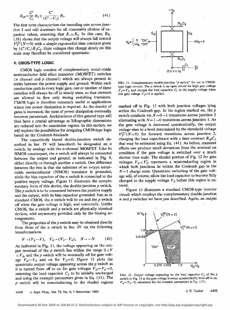
The capacitively biased double-junction switch de- scribed in Sec. IV will henceforth be designated an n swit& by analogy with the n-channel MOSFET. Like its NMOS counterpart, the IZ switch will always be connected between the output and ground, as indicated in Fig. 9, either directly or through another n switch. One difference between the two is that the substrate of an n-type metal- oxide semiconductor (NMOS) transistor is grounded, while the bias capacitor of the IZ switch is connected to the positive supply voltage. Figure 11 illustrates the comple- mentary form of this device, the double-junction p switch. Thep switch is to be connected between the positive supply and the output, with its bias capacitor grounded. Just as in standard Ch$OS, the n switch will be on and the p switch off when the gate voltage is high, and conversely. Unlike CMOS, the n switch and p switch are physically identical devices, with asymmetry provided only by the biasing ar- rangements.
The properties of thep switch may be obtained directly from those of the n switch in Sec. IV via the following twnsformations
v3 (Ff**- V), P-p (V,- V&, N- -iv. (42)
As indicated in Fig. 11, the voltage appearing on the out- put terminal of the p switch lies within the range O< V < vsl and the p switch will be nominally off for gate volt-
age Vo= Ys and on for Vo=O. Figure 12 plots the quasistatic output voltage appearing across the p switch as it is turned from off to on for gate voltages I’,= V,-tO, assuming the load capacitor CL to be initially uncharged and using the example paramet,ers given in Eq. (33). The p switch will be nonconducting in the shaded regions
4409 J. Appl. Phys., Vol. 72, No. 9, 1 November 1992
+vs 0
R2f-32
CG I A I Cl3
da **CL _-_--_- 4: ------- 4;; osvs; vs Ii
FIG. 11. Complementary double-junction “p switch” for use in CMOS- type logic circuits. The p switch is an open circuit for high gate voltage V,= Vs and charges the load capacitor CL to the supply voltage when low gate voltage V,=O is applied.
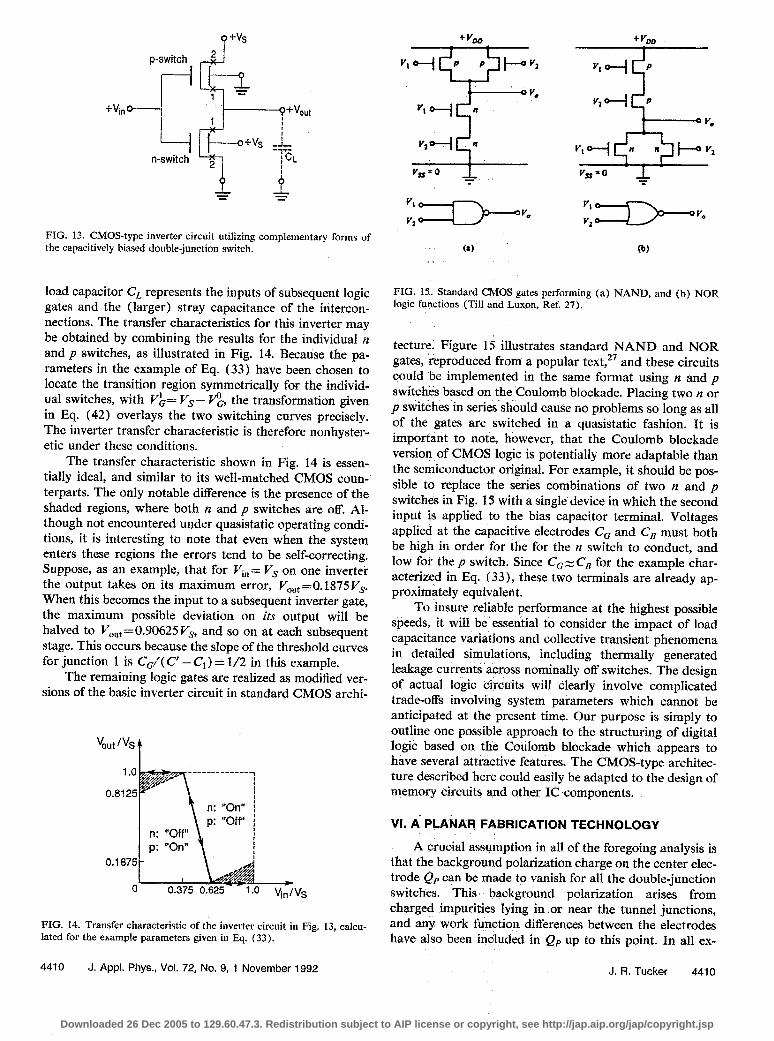
marked off in Fig. 12 with both junction voltages lying within the Coulomb gap. In the region marked on, the p switch conduc.ts via Jv=O-t 1 transitions across junction 2 alternating with N= 1-O transitions across junction 1. As the gate voltage is decreased quasistatically, the output voltage rises to a level determined by the threshold voltage @)(N=O) for forward transitions across junction 2, charging the load capacitance with a time constant RgL that may be estimated using Eq. (41). As before, transient effects can produce small deviations from the nominal on condition if the gate voltage is switched over a much shorter time scale. The shaded portion of Fig. 12 for gate voltages Vo< F’h represents a nonconducting region in which both junctions lie within the Coulomb gap in the N= 1 charge state. Quasistatic switching of the gate volt- age will, of course, allow the load capacitor to become fully charged to the supply voltage Vs before this region is en- tered.
Figure 13 illustrates a standard CMOS-type inverter circuit which employs the complementary double-junction n and p switches we have just described. Again, an output
WV, : f \ $%J-0)
1.0
0.8125
FIG. 12. Output voltage appearing on the load capacitor C, of the p switch in Fig. 11 as the gate voltage is swept quasistatically from off to on, ri,= V,-0, calculated for the example parameters in Eq. (33).
J. R. Tucker 4409
Downloaded 26 Dec 2005 to 129.60.47.3. Redistribution subject to AIP license or copyright, see http://jap.aip.org/jap/copyright.jsp
+Yn +vout
FIG. 13. CMOS-type inverter circuit utilizing complementary forms of the capacitively biased double-junction switch.
load capacitor CL represents the inputs of subsequent logic gates and the (larger) stray capacitance of the intercon- nections. The transfer characteristics for this inverter may be obtained by combining the results for the individual il and p switches, as illustrated in Fig. 14. Because the pa- rameters in the example of Eq. (33 9 have been chosen to locate the transition region symmetrically for the individ- ual switches, with I$= V,- v”o, the transformation given in Eq. (42) overlays the two switching curves precisely. The inverter transfer characteristic is therefore nonhyster- etic under these conditions.
The transfer characteristic shown in Fig. 14 is essen- tially ideal, and similar to its well-matched CMOS coun-’ terparts. The only notable difference is the presence of the shaded regions, where both n and p switches are off. Al- though not encountered under quasistatic operating condi- tions, it is interesting to note that even when the system enters these regions the errors tend to be self-correcting. Suppose, as an example, that for Fin= V, on one inverter the output takes on its maximum error, Y,,,=O.1875 V,. When this becomes the input to a subsequent inverter gate, the ma.ximum possible deviation on its output will be halved to J&=0.90625F7s, and so on at each subsequent stage. This occurs because the slope of the threshold curves for junction 1 is CJ( C-Cl9 = l/2 in this example.
The remaining logic gates are realized as modified ver- sions of the basic inverter circuit in standard CMOS archi-
1.0
0.8125
0.1875
T&s
FIG. 14. Transfer characteristic of the inverter circuit in Fig. 13, calcu- lated for the example parameters given in Eq. (33).
4410 J. Appl, Phys., Vol. 72, No. 9, 1 November 1992
?---
V, 6-j n
5-i p
L V.
Vrt’O 1, ~sF-.&$~~l
7 Y
(1) (a)
FIG. IS. Standard CMOS gates performing (a) NAND, and (b) NOR logic functions (Till and Luxon, Ref. 27).
tecture. Figure 15 illustrates standard NAND and NOR gates, reproduced from a popular text,” and these circuits could be implemented in the same format using n and p switches based on the Coulomb blockade. Placing two n or p switches in series should cause no problems so long as all of the gates are switched in a quasistatic fashion. It is important to note, however, that the Coulomb blockade version of CMOS logic is potentially more adaptable than the semiconductor original. For example, it should be pos- sible to replace the series combinations of two R and p switches in Fig. 15 with a single device in which the second input is applied to the bias capacitor terminal. Voltages applied at the capacitive electrodes C, and C, must both be high in order for the for the n switch to conduct, and low for the p switch. Since Co;=C, for the example char- acterized in Eq. (33), these two terminals are already ap- proximately equivalent.
To insure reliable performance at the highest possible speeds, it will be essential to consider the impact of load capacitance variations and collective transient phenomena in detailed simulations, including thermally generated leakage currents across nominally off switches. The design of actual logic circuits will clearly involve complicated trade-offs involving system parameters which cannot be anticipated at the present time. Our purpose is simply to outline one possible approach to the structuring of digital logic based on the Coulomb blockade which appears to have several attractive features. The CMOS-type architec- ture described here could easily be adapted to the design of memory circuits and other IC components.
VI. A PLANAR FABRICATION TECHNOLOGY
A crucial assumption in all of the foregoing analysis is that the background polarization charge on the center elec- trode Qp can be made to vanish for all the double-junction switches. This background polarization arises from charged impurities lying in or near the tunnel junctions, and any work function differences between the electrodes have also been included in Qp up to this point. In all ex-
J. Ft. Tucker 4410
Downloaded 26 Dec 2005 to 129.60.47.3. Redistribution subject to AIP license or copyright, see http://jap.aip.org/jap/copyright.jsp
periments performed to date, the value of Qp is effectively a random variable having uniform probability distribution over the interval -e/2 < Qp (e/2. Larger values of Qp are reduced into this range by the tunneling of additional elec- trons on or off the center electrode. Nonvanishing back- ground polarization charge introduces a random compo- nent onto the voltage of each center electrode, making it impossible to realize digital logic in the form of simple on/off switches without separately adjusting the capacitive bias applitd to each individual device.
This problem must be overcome in order to make large-scale circuits based on the Coulomb blockade a prac- tical possibility, and there are two differing viewpoints on how this might be accomplished. One view, outlined in a reoent review article by Averin and Likharev,” anticipates that the problem will simply disappear for sufficiently small electrodes and an appropriate choice of oxide barrier. Early work by Lambe and Jaklevics on Coulomb charging effects in ultrasmall junction-capac.itor arrays, described in Sec. I, noted an apparent tendency for the Fermi levels of the center droplets to align with the applied dc bias voltage over time scales on the order of several minutes at liquid- He temperatures. They attributed this memory effect to slow relaxation processes occurring within the oxide bar- riers, which were observed to be greatly accelerated by exposure to light or higher tempemtures. If the relaxation is due to diEusion of charges within the amorphous oxide, one might hope to freeze their distribution in order to null out the background polarization if the temperature To at which diffusion effectively ceases lies lower than the tem- perature scale, Te=ee3-/2kgC, of the Coulomb charging energy.
Recent work on the memory effect by Cavicchi and Silsbeeag however, has called irlto serious question the no- tion that polarization in the amorphous oxide tends to align the Fermi levels of the individual droplets, as implied by Lambe and Jaklevic. They point out that polarization processes within the oxide barriers are driven by electric fields, and that t.he electrostatic potential difference be- tween a droplet and a nearby electrode is distinct from the difIerence in Fermi levels when the work fun&ions are not identical. Because work functions measured on different crystal faces of a metal typically differ by tenths of volts, one expec.ts a random distribution of similar magnitude among the very small droplets in a Lambe-Jaklevic exper- iment, depending upon an individual particle’s shape and orientation. These random work function variations are therefore espected to be large compared to typical charg- ing energies. Cavicchi and Silsbee explicitly demonstrate, within the context of two generic models, that the freezing of polarization within the oxide will not act to align the Fermi levels of the individual droplets under these condi- tions. According to their interpretation, freezing polariza- tion has the effect of eliminating the probability for drop- lets to have reduced work functions which place their Fermi levels close to the tunneling thresholds at j=e/2C’, thereby narrowing the originally uniform distribution of droplet Fermi levels within the range -e/2C’ < EF < e/
2C’ and creating the capacitance hole observed in the memory effect.
Although the detailed arguments of Cavicchi and Sils- bee are lengthy, the essential idea for our purposes may be apprec.iated by considering the following special case. Imagine a center electrode whose work function differs from the external electrodes by an amount less than AC/ 2C’, so that its Fermi level is displaced anywhere within the Coulomb gap. The neutral N=O charge state will then remain stable at low temperatures, and the electric field across t.he oxide tunnel barriers will vanish for zero exter- nal bias in the absence of charged defects. In this case, there is a Fermi level difference due to the variation in work functions but no electric field that could drive a com- pensating polarization. Thus, any differences in work func- tion will need to be kept very small on the scale of e/2C’ if Fermi levels of all electrodes are to be aligned at zero bias voltage. Introducing a large density of mobile charges and/ or defects and then freezing them out will not succeed unless this condition is satisfied. Inclusion OF work function differences within an effective background polarization charge Qp is an acceptable expedient when calculating the tunneling rates for transfer of electrons across the junc- tions, but not when it comes to analyzing the effects of oxide polarization.
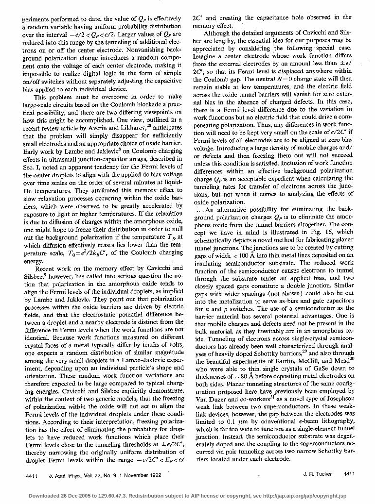
An alternative possibility for eliminating the back- ground polarization charges Qp is to eliminate the amor- phous oxide from the tunnel barriers altogether. The con- cept we have in mind is illustrated in Fig. 16, which schematically depicts a novel method for fabricating planar tunnel junctions. The junctions are to be created by cutting gaps of width < 100 A into thin metal lines deposited on an insulating semiconductor substrate. The reduced work function of the semiconductor causes electrons to tunnel through the substrate under an applied bias, and two closely spaced gaps constitute a double junction. Similar gaps with wider spacings [not shown) could also be cut into the metalization to serve as bias and gate capacitors for n and p switches. The use of a semiconductor as the barrier material has several potential advantages. One is that mobile charges and defects need not be present in the bulk material, as they inevitably are in an amorphous ox- ide. Tunneling of electrons across single-crystal semicon- ductors has already been well characterized through anal- yses of heavily doped Schottky barriers,25 and also through the beautiful experiments of Kurtin, McGill, and Mead3” who were able to thin single c.rystals of GaSe down to thicknesses of - 80 A before depositing metal electrodes on both sides. Planar tunneling structures of the same config- uration proposed here have previously been employed by Van Duzer and co-workers”’ as a novel type of Josephson weak link between two superconductors. in these weak- link devices, however, the gap between the electrodes was limited to 0.1 pm by conventional e-beam lithography, which is far too wide to function as a single-element tunnel junction. Instead, the semiconductor substrate was degen- erately doped and the coupling to the superconductors oc- c.urred via pair tunneling across two narrow Schottky bar- riers located under each electrode,
4411 J. Appi. Phys., Vol. 72, No. 9, 1 November 1992 J. FL Tucker 4411
Downloaded 26 Dec 2005 to 129.60.47.3. Redistribution subject to AIP license or copyright, see http://jap.aip.org/jap/copyright.jsp
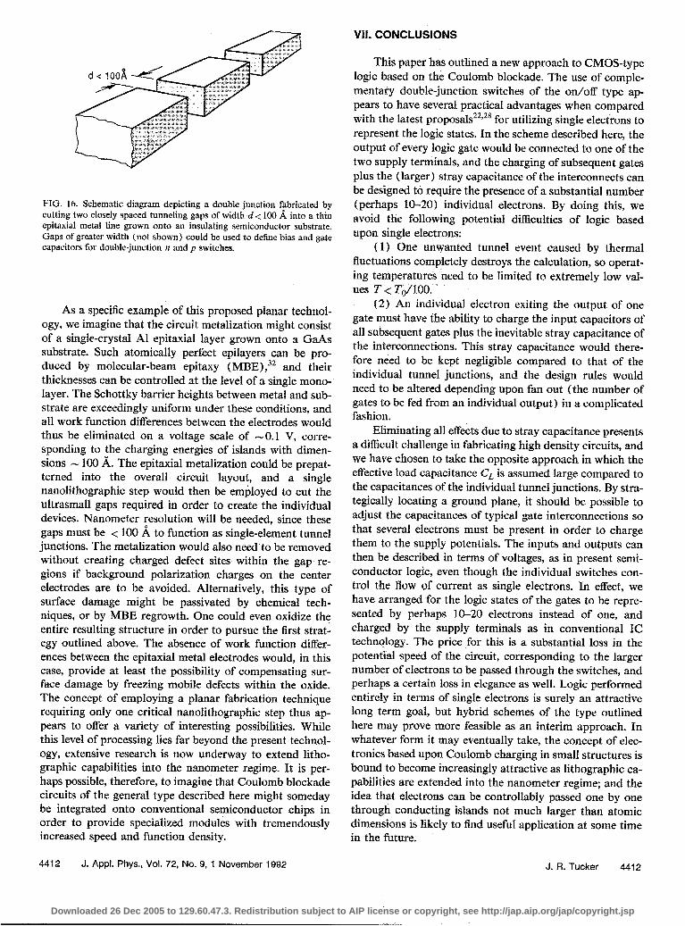
FIG. 16. Schematic diagram depicting a double junction fabricated by cutting two closely spaced tunneling gaps of width d < 100 A into a thin epitaxial metal line grown onto an insulating semiconductor substrate. Gaps of greater width (not shown) could be used to define bias and gate capacitors for double-junction n and p switches.
As a specific example of this proposed planar technol- ogy, we imagine that the circuit metalization might consist of a single-crystal Al epitaxial layer grown onto a GaAs substrate. Such atomically perfect epilayers can be pro- duced by molecular-beam epitaxy (MBE),32 and their thicknesses can be controlled at the level of a single mono- layer. The Schottky barrier heights between metal and sub- strate are exceedingly uniform under these conditions, and all work function differences between the electrodes would thus be eliminated on a voltage scale of -0.1 V, corre- sponding to the charging energies of islands with dimen- sions - 100 A. The epitaxial metalization could be prepat- terned into the overall circuit layout, and a single nanolithographic step would then be emmoyed to cut the ultrasmall gaps required in order to create the individual devices. Nanometer resolution will be needed, since these gaps must be < 100 A to function as single-element tunnel junctions. The metalization would also need to be removed without creating charged defect sites within the gap re- gions if background polarization charges on the center electrodes are to be avoided. Alternatively, this type of surface damage might be passivdted by chemical tech- niques, or by MBE regrowth. One could even oxidize the entire resulting structure in order to pursue the first strat- egy outlined above. The absence of work function differ- ences between the epitaxial metal electrodes would, in this case, provide at least the possibility of compensating sur- face damage by freezing mobile defects within the oxide. The concept of employing a planar fabrication technique requiring only one critical nanolithographic step thus ap- pears to offer a variety of interesting possibilities. While this level of processing lies far beyond the present technol- ogy, extensive research is now underway to extend litho- graphic capabilities into the nanometer regime. It is per- haps possible, therefore, to imagine that Coulomb blockade circuits of the general type described here might someday be integrated onto conventional semiconductor chips in order to provide specialized modules with tremendously increased speed and function density.
VII. CONCLUSIONS
This paper has outlined a new approach to CMOS-type logic based on the Coulomb blockade. The use of comple- mentary double-junction switc.hes of the on/off type ap- pears to have several practical advantages when compared with the latest proposals’2*28 for utilizing single electrons to represent the logic states. In the scheme described here, the output of every logic gate would be connected to one of the two supply terminals, and the charging of subsequent gates plus the (larger) stray capacitance of the interconnects can be designed to require the presence of a substantial number (perhaps 10-20) individual elec.trons. By doing this, we avoid the following potential difficulties of logic based upon single electrons:
( 1) One unwanted tunnel event caused by thermal fluctuations completely destroys the calculation, so operat- ing temperatures need to be Iimited to extremely low val- ues T< TdlOO.
(2) An individual electron exiting the output of one gate must have the ability to charge the input capacitors of all subsequent gates plus the inevitable stray capacitance of the interconnections. This stray capacitance would there- fore need to be kept negligible compared to t,hat of the individual tunnel junctions, and the design rules would need to be altered depending upon fan out (the number of gates to be fed from an individual output) in a complicated fashion.
Eliminating all effec.ts due to stray capacitance presents a difficult challenge in fabricating high density circuits, and we have chosen to take the opposite approach in which the effective load capacitance CL is assumed large compared to the capacitances of the individual tunnel junctions. By stra- tegically locating a ground plane, it should be possible to adjust the capacitances of typical gate interconnections so that several electrons must be present in order to charge them to the supply potentials. The inputs and outputs can then be described in terms of voltages, as in present semi- conductor logic, even though the individual switches con- trol the flow of current as single electrons. In effect, we have arranged for the logic states of the gates to be repre- sented by perhaps 10-20 electrons instead of one, and charged by the supply terminals as in conventional IC technology. The price for this is a substantial loss in the potential speed of the circuit, corresponding to the larger number of electrons to be passed through the switches, and perhaps a certain loss in elegance as well. Logic performed entirely in terms of single electrons is surely an attractive long term goal, but hybrid schemes of the type outlined here may prove more feasible as an interim approach. In whatever form it may eventually take, the concept of elec- tronics based upon Coulomb charging in small structures is bound to become increasingly attractive as lithographic ca- pabilities are extended into the nanometer regime; and the idea that electrons can be controllably passed one by one through conducting islands not much larger than atomic dimensions is likely to find useful application at some time in the future.
4412 J. Appl. Phys., Vol. 72, No. 9, ‘I November 1992 J. FL Tucker 4412
Downloaded 26 Dec 2005 to 129.60.47.3. Redistribution subject to AIP license or copyright, see http://jap.aip.org/jap/copyright.jsp
ACKNOWLEDGMENTS
This work has been supported by the National Science Foundation under Grant No. DMR-8920538 through the Materials Research Laboratory at the University of Illinois and by the U.S. Joint Services Electronics Program under Contract No. NOOO14-90-J-1270. The author thanks Dr. K. I(. Likharev for a critical reading of the manuscript.
‘R. T. Bate, Nanotechnoiog>~ 1, 1 (1990). “R. P. Feynman, “There’s Plenty of Room at the Bottom,” in Science and Technology (California Institute of Technology), February, 1960.
‘K. K. Likharev, IEEE Trans. Magn. MAG-23, 1 I42 (1987). ’ Proceedings of the F$h International Conference on Scannittg TutmeG
ing ,~ictr~cupy and First International Conference on Na- ROJJZ&T SC& Science and Technology, edited by R. J. Colton, C. K. R. Mar&m, and J. A. Strocio (American Vacuum Society, New York, 1991).
“C. J, Gorter, Physica 17, 778 (1951). ‘C. A. Neugebauer and M. B. Webb, J. Appl. Phys. 33, 74 (1962). “I. Girrevcr and H. R. Zdler, Phys. Rev. Lett. 20, 1504 ( 1968); H. R.
Zellcr and T. Giaever, J. Vat. Sci. Technoi. 6, 502 (1969). “J. Lambe and R. C. Jaklevic, Phys. Rev. Lett. 22, 1371 ( 1969). “R. E. Cavicchi and R. H. Silsbee, Phys. Rev. Lett. 52, 1453 (1984);
Phhgs. Rev. B 37. 707 ( 1935); ibid. 38, 6407 (1988). “D. V. Averin and K. El. Likharev: in Proceedings offhe Third Interna-
tii?nul Conference on Superconducting Quantum Devices {SQUIDS), Ber- lin, 1985, edited by H. D. Hahibohm and H. L&big (de Gruyter, New York, 1985), p. 197; J. Low Temp. Phys. 62, 345 (1986).
l1 E. Ben-Jacob, Y. Gefen, K. Mullen, and Z. Schuss, in Ptwceedfngs of the Third I~tternaticmal Conference Ron Superconduciing Quantum Devices ISQUiDs), Berlin, 1985, edited hy H. D. Hahibohm and H. Lubbig (de Gruyter, New York, 1985), p. 20-1; Phys. Rev. B 37, 74CO (1988); E. Ben-Jacob, D. I. Bergman, B. J. Matkowsky, and Z. Schuss, ibid. 34, 1572 (1986); K. Mullen. E. Ben-Jacob, R. C. Jaklevic, and Z. Schuss, ibid. 37, 98 (I%%).
“I. 0. Kuiik and R. I. Shekhter, Sov. Phys. JETP 41, 308 (1975). riL, S. Kuzmin and K. K. Likharev, Pis’mn, Zh. Eksp. Theor. Fiz. 45,
389 (1987) [JETP Lett. 45,495 (1987)].
14J. B. Bamer and S. T. Rug&o, Phys. Rev. Lett. 59, 807 (1987). 15P J M. van Bentum, R. T. M. Smokers, and H. van Kempen, Phys.
Rev. Lett. 60, 2543 (1988); P. J. M. van Bentum, L. E. C. van de Leemput, R. T. M, Smoker% and H. van Kempen, J. Micros. 152, 11 [ 1988).
“R. Wilkins, E, Ben-Jacob, and R C. Jakievic, Phys. Rev. L&t. 63, 801 (1989).
‘7J.-C. Wan, K. A. hlcGreer, N. Anend, E. Nowak, and A. M. Goldman, Phys. Rev. B 42, 5604 (1990).
‘*T. A. Fuiton and G. J. Doian, Phys. Rev. Lett. 59, 109 (1987). 19L. S. Kuzmin, P. Deising, T. Ciaeson, and K. K. Likharev, Phys. Rev.
Lett. 62, 2539 (1989). ‘OP. Deising, K. K. Likharev, L. S. Kuzmin, and T. Claeson, Phys. Rev.
Lett. 63, 1861 (1989). “L. J. Geeriigs, V. F. Anderegg, P. A. M. Hoiweg, J. E. Mooij, H.
Pothier, D. F&eve., C. Urbina, and M. H. Devoret, Phys. Rev. Lett, 64, 2691 (1990).
“K. K. Likharev, 5. F. Poionsky, and S. V. Vyshensky (to be published). ‘jU. Meirav, M. A. Kastner, and S. J. Wind, Phys. Rev. Lett. 65, 771
(1990). “K. K. Likharev, IBM J. Res. Dev. 32, 144 (1988). “D. V. Averin and K. K, Likharev, “Single-Electronics,” in Quantum
Effects in Small Disordered Systems, edited by B. L. Aitschuier, P. A. Lee, and R. A. Webb (Elsevier, Amsterdam, 1990).
26T. A. Fuiton, P. L. Gammel, D. J. Bishop, L. N. Dunkieberger, and G. J. Doian, Phys. Rev. I..&. 63, 1307 ( 1989).
27 W. C. Till and J. T. Luxon, Integrated Circuits: Marerials, Devicrs, and Fabrication (Prentice-Hail, Engiewood Cliffs, NJ, 1982).
“D. V. Averin and K. K. Likharev, in Single-Charge Tunneling, edited by M. Devoret and H. Grabert (Plenum, New York) (to be published).
‘gfee, for example, J. W. Coniey, C. B. Duke, G. D. Mahan, and J. J. Tiemann, Phys. Rev. 150,466 ( 1966); G. D. Mahan and J. W. Coniey, Appl. Phys. L&t. 11,29 (1967); G. H. Parker and C. A. Mead, Phys. Rev. 184, 780 (1969).
3uS L. Kurtin, T. C. McGill, and C. A. Mead, Phys. Rev, B 3, 3368 (i971).
3’M. Schyfter, J. Maah-Sango, N. Raiey, R. Ruby, B. T. Wirich, and T. Van Duzer, IEEE Trans. Magn. M A G 13, 862 ( 1977).
“G. Landgren, R. Ludeke, and C. Serrano, J. Cry& Growth 60, 393 (1982).
4413 J. Appi. Phys., Vol. 72, No. 9, 1 November 1992 J. R. Tucker 4413
Downloaded 26 Dec 2005 to 129.60.47.3. Redistribution subject to AIP license or copyright, see http://jap.aip.org/jap/copyright.jsp